eeng410/infe410 – microprocessors i · pdf file¾ the address and control bus...
TRANSCRIPT

EENG410/INFE410 – Microprocessors I Fall 08/09 – Lecture Notes # 1
Outline of the Lecture Microcomputers and Microprocessors Evolution of Intel 80x86 Family Microprocessors Binary and Hexadecimal Number Systems
MICROCOMPUTERS AND MICROPROCESSORS
There are three major parts of a Computer System.
1. Central Processing Unit (CPU): Also simply called as the microprocessor acts as the brain coordinating all activities within a computer.
2. The Memory: The program instructions and data are primarily stored. 3. The Input/Output (I/O) Devices: Allow the computer to input information for processing and
then output the results. I/O Devices are also known as computer peripherals.
The integrated Circuit (IC) chip containing the CPU is called the microprocessor and the entire computer including the microprocessor, memory and I/O is called a microcomputer.
The CPU is connected to memory and I/O devices through a strip of wires called a bus. The bus inside a computer carries information from place to place. In every computer there are three types of busses:
1. Address Bus: The address bus is used to identify the memory location or I/O device the processor intends to communicate with. The width of the Address Bus rages from 20 bits (8086) to 36 bits for (Pentium II).
2. Data Bus: Data bus is used by the CPU to get data from / to send data to the memory or the I/O devices. The width of a microprocessor is used to classify the microprocessor. The size of data bus of Intel microprocessors vary between 8-bit (8085) to 64-bit (Pentium).
3. Control Bus. How can we tell if the address on the bus is memory address or an I/O device address? This where the control bus comes in. Each time the processor outputs an address it also activates one of the four control bus signals: Memory Read, Memory Write, I/O Read and I/O Write.
The address and control bus contains output lines only, therefore it is unidirectional, but the data bus is bidirectional.
There two types of memory used in microcomputers: ♦ RAM (Random Access Memory/ Read-Write memory) is used by the computer for the temporary
storage of the programs that is running. Data is lost when the computer is turned off. So known as volatile memory.
♦ ROM (Read Only Memory) the information in ROM is permanent and not lost when the power is turned off. Therefore, it is called nonvolatile memory.
Note that RAM is sometimes referred as primary storage, where magnetic /optical disks are called secondary storage.

Internal organisation of a microcomputer Inside the CPU: A program stored in the memory provides instructions to the CPU to perform a specific action. This action can be a simple addition. It is function of the CPU to fetch the program instructions from the memory and execute them.
1. The CPU contains a number of registers to store information inside the CPU temporarily. Registers inside the CPU can be 8-bit, 16-bit, 32-bit or even 64-bit depending on the CPU.
2. The CPU also contains Arithmetic and Logic Unit (ALU). The ALU performs arithmetic (add, subtract, multiply, divide) and logic (AND, OR, NOT) functions.
3. The CPU contains a program counter also known as the Instruction Pointer to point the address of the next instruction to be executed.
4. Instruction Decoder is a kind of dictionary which is used to interpret the meaning of the instruction fetched into the CPU. Appropriate control signals are generated according to the meaning of the instruction.
Internal block diagram of a CPU
CPU
Read/
Write
RAM ROM Printer Disk Monitor Keyboard
Address Bus
Data Bus
Control Bus
Flags
ALU
Instruction Pointer
Instruction Register
Instruction Decoder Timing and control
signals are generated
Register BRegister A
Register DRegister C
Address Bus
Control Bus Data Bus
Internal Busses

The Figure below demonstrates the interaction between the CPU, memory and I/O Devices.

Brief History of the Computers • 1946 The first generation of Computer ENIAC was started to be used based on the vacuum tube
technology. • 1958 the first transistorized computer TRADIC was announced by IBM. • 1959 first IC was invented. • 1960s ICs were started to be used in CPU boards. • 1970s entire CPU was put in a single chip. (1971 the first microprocessor of Intel 4004 (4-bit data bus
and 2300 transistors) • Late 1970s Intel 8080/85 appeared with 8-bit data bus and 16-bit address bus and used from traffic light
controllers to homemade computers. • 1981 First PC was introduced by IBM with Intel 8088 microprocessor. • Motorola emerged with 6800. Apple Macintosh computers started to use 68000 series of
microprocessors.
EVOLUTION OF INTEL 80X86 FAMILY MICROPROCESSORS Processor Year
Intro. Transistors Clock Rate
(MHz.) External Data Bus
Internal Data Bus
Add. Bus
4004 1971 2,250 0.108 4 8 12 8008 1972 3,500 0.200 8 8 14 8080 1974 6,000 3 8 8 16 8085 1976 6,000 6 8 8 16 8086 1978 29,000 10 16 16 20 8088 1979 29,000 10 8 16 20 80286 1982 134,000 12.5 16 16 25
80386DX 1985 275,000 33 32 32 32 80386SX 1988 275,000 33 16 32 24 Pentium C 1993 3,100,000 66 -200 64 32 32
Pentium MMX 1997 4,500,000 300 64 32 32 Pentium Pro 1995 5,500,000 200 64 32 36 Pentium II 1997 7,500,000 233-450 64 32 36 Pentium III 1999 9,500,000 550-733 64 32 36
Itanium 2001 30,000,000 800-… 128 64 64
BINARY AND HEXADECIMAL NUMBER SYSTEMS As human being we use base 10 (decimal) arithmetic Computers use base 2 (binary) system. Base 16 Hexadecimal number system is a convenient way of represented binary numbers. ASCII (binary format of the alphanumeric code) is explained. Decimal and Binary number systems:
-There is a speculation of the fact that Humans use base 10 system is because they have 10 fingers. But there is no speculation behind the fact that the computers use binary system. The binary system is used in computers, because 1 and zero represent the two voltage levels of on and off. There are 10 digits in Decimal system: 0,1,2,3,4,5,6,7,8,9 There are only 2 digits in Binary system: 0,1 (Binary digits are referred as bits)

Converting from decimal to binary: Example: Convert 2510 to binary: Remainder 25/2 = 12 1 LSB (least significant bit) 12/2 = 6 0 6/2 = 3 0 3/2 = 1 1 1/2 = 0 1 MSB (most significant bit) Therefore, 2510 = 110012 Converting from binary to decimal: Example: Convert 1101012 to decimal: 1101012 = Decimal 1x20 =1x1 = 1
0x21 =0x2 = 0 1x22 =1x4 = 4 0x23 =0x8 = 0 1x24 =1x16 = 16 1x25 =1x32 = + 32 53 1101012 =5310 Hexadecimal Number system: Hexadecimal system is defined to be the base 16 number system and is used as a convenient representation of binary numbers. Hexadecimal Binary Decimal 0 0000 0 1 0001 1 2 0010 2 3 0011 3 4 0100 4 5 0101 5 6 0110 6 7 0111 7 8 1000 8 9 1001 9 A 1010 10 B 1011 11 C 1100 12 D 1101 13 E 1110 14 F 1111 15
Converting from binary to hex (hexadecimal): Example: Convert 1001111101012 to hex: 1001 1111 0101 = 9 F 5 Therefore, 1001111101012 = 9F5 Hex Converting from hex to binary: Example: Convert hex 29B to binary: 2 9 B = 0010 1001 1011 Dropping zeros, 29B = 1010011011

Converting from decimal to hex (hexadecimal): Example: Convert 4510 to hex: Quotient Remainder 45/16 = 2 13 (hex D) LSD (least significant bit) 2/16 = 0 2 MSD (most significant bit) Therefore, 4510 = 2D16 = 2DH Converting from hex to decimal: Example: Convert 6B216 to decimal: 6B216 = Decimal 2 x 160 = 2 x 1 = 2 11x161 = 11x16 = 176
6 x 162= 6x256 = + 1536 1714 Therefore, 6B216 = 171410
Addition and subtraction in binary numbers: Addition Example:
Subtraction of Binary Numbers: Given binary numbers x and y. x–y is performed by taking 2’s complement of y and adding to x. 11001001 – 10011101 => 2’s complement of 10011101= 01100010 (1’s complement) +1 01100011 (2’s complement)
11001001 + 01100011 1 00101100 Addition and subtraction in hex numbers: Addition Example:
Subtraction Example:
1101 1001 + 10110 101100
A + B Carry Sum 0 + 0 0 0 0 + 1 0 1 1 + 0 0 1 1 + 1 1 0
Binary Addition
23D9 LSD : 9 + 14 = 23 23-16= 7 with a carry to next digit + 94BE 1+13+11 = 25 25-16= 9 with a carry to next digit B897 1+3+4 = 8 MSD 2 + 9 = B
59F LSD : 15 - 8 = 7 – 2B8 25 (9+16) – 11 (B) = 14, which is E
2E7 MSD 4 (5–1) –2 = 2

ASCII Code : (American Standard Code for Information Interchange) Hex Symbol Hex Symbol 41 A 61 a 42 B 62 b 42 C 62 c 44 D 64 d 45 E 65 e 46 F 66 f 47 G 67 g 48 H 68 h 49 I 69 i 4A J 6A j 4B K 6B k 4C L 6C l 4D M 6D m 4E N 6E n 4F O 6F o 50 P 70 p 51 Q 71 q 52 R 72 r 53 S 73 s 54 T 74 t 55 U 75 u 56 V 76 v 57 W 77 w 58 X 78 x 59 Y 79 y 5A Z 7A z Some important terminology: bit 0 nibble 0000 byte 0000 0000 word 0000 0000 0000 0000 double-word 0000 0000 0000 0000 0000 0000 0000 0000 quad-word 0000 0000 0000 0000 0000 0000 0000 0000 0000 0000 0000 0000 0000 0000 0000 0000 1 kilobyte is 210 bytes. (Abbreviation K is used) Some floppy disks hold 356K bytes of data. 1 megabyte is 220 bytes. (a little over a million 1,048,576) 1 gigabyte is 230 bytes (over 1 trillion) 1 terabyte is 240 bytes

EEE 410 – Microprocessors I Fall 05/06 – Lecture Notes # 2
Outline of the Lecture Brief History of 80x86 Family of Microprocessors Pipelining and Registers Introduction to Assembly Programming
BRIEF HISTORY OF 80X86 FAMILY OF MICROPROCESSORS
Evolution from 8080/8085 to 8086
Intel introduced 8086 microprocessor in 1978. This 16-bit microprocessor was a major improvement over the previous generation of 8080/8085 series of microprocessors.
8086 8080/8085
1 megabyte (20-bit add. bus)
Memory of 64 kilobyte (16-bit add. bus)
16-bit Data bus 8-bit data bus Pipelined processor (first single-chip µpr.)
Non-pipelined µpr
In a system with pipelining, the data and the address bus are busy transferring data while the CPU is
processing information. Evolution from 8086 to 8088
8086 was with 16-bit data bus internally and externally. All registers and the data bus carrying data in/out of the CPU were 16-bit.
• That time all the peripherals were designed around 8-bit microprocessor. • It was expensive to built PCB with 16-bit data bus.
So Intel introduced 8088 which was;
• Identical to 8086 internally, but externally 8-bit data bus instead of 16-bit. • It had 1 megabyte of memory like 8086.
IBMs decision to pick up 8088 as their choice of microprocessor in designing the IBM PC.
• 8088-based IBM PC was enormous success, because IBM and Microsoft made it an open system.
• This enabled the cloning of this system and resulted a huge growth in both hardware and software designs based on IBM PC.
• In contrast IBMs main competitor Apple computer introduced a closed system and blocked all attempts of cloning.
Other microprocessors: the 80286, 80386, and 80486
80286: Intel introduced 80286 in 1982. • With 16-bit internal and external data bus. • 24-bit address bus (224 = 16 megabyte) • virtual memory: a way of fooling the microprocessor into thinking that it has access to unlimited
memory by swapping data between disk storage and RAM. • Real mode (faster operation with maximum of 1 Mbytes of memory) vs. Protected mode
protecting the operating system for accidental or deliberate destruction of the user. Protected mode is slower but can use 16 Mbytes of memory.
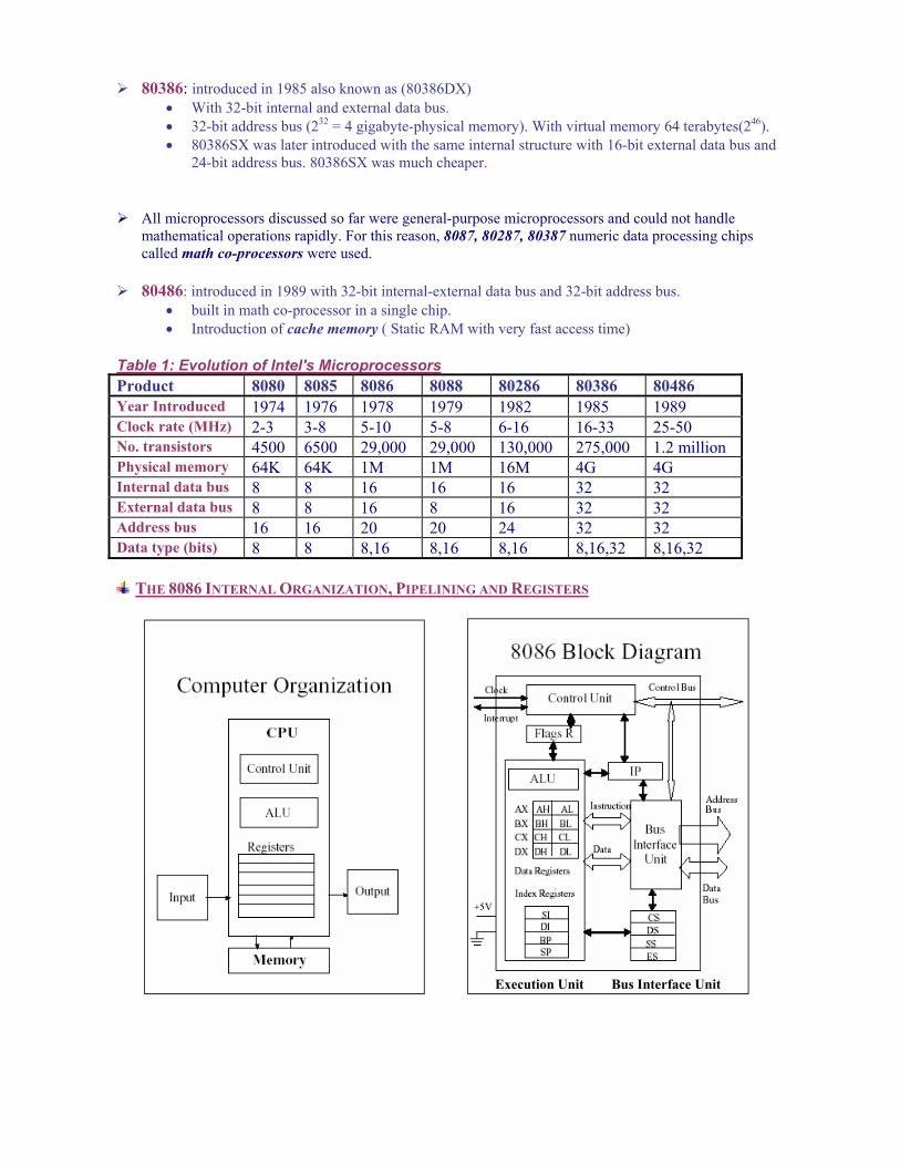
80386: introduced in 1985 also known as (80386DX) • With 32-bit internal and external data bus. • 32-bit address bus (232 = 4 gigabyte-physical memory). With virtual memory 64 terabytes(246). • 80386SX was later introduced with the same internal structure with 16-bit external data bus and
24-bit address bus. 80386SX was much cheaper.
All microprocessors discussed so far were general-purpose microprocessors and could not handle mathematical operations rapidly. For this reason, 8087, 80287, 80387 numeric data processing chips called math co-processors were used.
80486: introduced in 1989 with 32-bit internal-external data bus and 32-bit address bus.
• built in math co-processor in a single chip. • Introduction of cache memory ( Static RAM with very fast access time)
Table 1: Evolution of Intel's Microprocessors Product 8080 8085 8086 8088 80286 80386 80486 Year Introduced 1974 1976 1978 1979 1982 1985 1989 Clock rate (MHz) 2-3 3-8 5-10 5-8 6-16 16-33 25-50 No. transistors 4500 6500 29,000 29,000 130,000 275,000 1.2 million Physical memory 64K 64K 1M 1M 16M 4G 4G Internal data bus 8 8 16 16 16 32 32 External data bus 8 8 16 8 16 32 32 Address bus 16 16 20 20 24 32 32 Data type (bits) 8 8 8,16 8,16 8,16 8,16,32 8,16,32
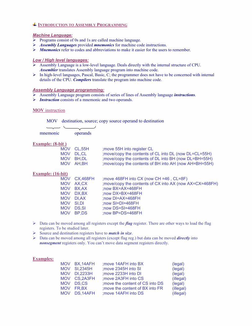
THE 8086 INTERNAL ORGANIZATION, PIPELINING AND REGISTERS
Execution Unit Bus Interface Unit

Pipelining
In the 8085 microprocessor, the CPU could either fetch or execute at a given time. CPU had to fetch an instruction from the memory, then execute it, then fetch again and execute it and so on..
Pipelining is the simplest form to allow the CPU to fetch and execute at the same time. Note that the fetch and execute times can be different.
Pipelined vs. Nonpipelined Execution
Intel implemented the concept of pipelining by splitting the internal structure of 8088/86 into two sections.
• the execution unit (EU) • the bus interface unit (BIU) • These two sections work simultaneously. BIU accesses memory and peripherals while the EU
executes the instructions previously fetched. • It only works if BIU keeps ahead of EU. Thus BIU has a buffer of queue. (8088 has 4 byte, and
8088 has 6 bytes). • If the execution of any instruction takes to long, the BIU is filled to its maximum capacity and
busses will stay idle. It starts to fetch again whenever there is 2-byte room in the queue. • When there is a jump instruction, the microprocessor must flush out the queue. When a jump
instruction is executed BIU starts to fetch information from the new location in the memory. In this situation EU must wait until the BIU starts to fetch the new instruction. This is known as branch penalty.
nonpipelined fetch 1 exec 1 fetch 2 exec 2 (e.g.. 8085)
pipelined fetch 1 exec 1 (e.g. 8086)
fetch 2 exec 2
fetch 3 exec 3

Registers of 8086 Microprocessor
In the CPU, registers are used store information temporarily. The information can be one or two bytes of data, or the address of data.
In 8088/8086 general-purpose registers can be accessed as either16-bit or 8-bit registers. All other registers can be accessed as full 16-bit registers.
The bits of the registers are numbered in descending order:
8-bit register:
D7 D6 D5 D4 D3 D2 D1 D0
16-bit register: D15 D14 D13 D12 D11 D10 D9 D8 D7 D6 D5 D4 D3 D2 D1 D0
Different registers are used for different functions. Registers will be explained later within the context of instructions and their applications.
The first letter of each general register indicates its use. • AX is used for the accumulator. • BX is used for base addressing register. • CX is used for counter loop operations. • DX is used to point out data in I/O operations.
Registers of 8086 Category Bits Register Names
16 AX, BX, CX, DX General 8 AH, AL, BH, BL, CH, CL, DH, DL
Pointer 16 SP (stack pointer), BP(base pointer) Index 16 SI (source index), DI(destination index) Segment 16 CS (code segment), DS(data segment)
SS (stack segment), ES(extra segment) Instruction 16 IP (instruction pointer) Flag 16 FR (flag register)
Note: the general registers can be accessed as full 16 bits (such as AX), or as the high byte only (AH) or low byte only (AL). The others are not!!
AX16-bit register
AH AL
8-bit reg. 8-bit reg.
INTRODUCTION TO ASSEMBLY PROGRAMMING Machine Language:
Programs consist of 0s and 1s are called machine language. Assembly Languages provided mnemonics for machine code instructions. Mnemonics refer to codes and abbreviations to make it easier for the users to remember.
Low / High level languages:
Assembly Language is a low-level language. Deals directly with the internal structure of CPU. Assembler translates Assembly language program into machine code.
In high-level languages, Pascal, Basic, C; the programmer does not have to be concerned with internal details of the CPU. Compilers translate the program into machine code.
Assembly Language programming:
Assembly Language program consists of series of lines of Assembly language instructions. Instruction consists of a mnemonic and two operands.
MOV instruction MOV destination, source; copy source operand to destination
mnemonic operands Example: (8-bit )
MOV CL,55H ;move 55H into register CL MOV DL,CL ;move/copy the contents of CL into DL (now DL=CL=55H) MOV BH,DL ;move/copy the contents of DL into BH (now DL=BH=55H) MOV AH,BH ;move/copy the contents of BH into AH (now AH=BH=55H) Example: (16-bit)
MOV CX,468FH ;move 468FH into CX (now CH =46 , CL=8F) MOV AX,CX ;move/copy the contents of CX into AX (now AX=CX=468FH) MOV BX,AX ;now BX=AX=468FH MOV DX,BX ;now DX=BX=468FH MOV DI,AX ;now DI=AX=468FH
MOV SI,DI ;now SI=DI=468FH MOV DS,SI ;now DS=SI=468FH MOV BP,DS ;now BP=DS=468FH
Data can be moved among all registers except the flag register. There are other ways to load the flag
registers. To be studied later. Source and destination registers have to match in size. Data can be moved among all registers (except flag reg.) but data can be moved directly into
nonsegment registers only. You can’t move data segment registers directly. Examples:
MOV BX,14AFH ;move 14AFH into BX (legal) MOV SI,2345H ;move 2345H into SI (legal) MOV DI,2233H ;move 2233H into DI (legal) MOV CS,2A3FH ;move 2A3FH into CS (illegal) MOV DS,CS ;move the content of CS into DS (legal) MOV FR,BX ;move the content of BX into FR (illegal) MOV DS,14AFH ;move 14AFH into DS (illegal)

Important points: • Values cannot be loaded directly into (CS,DS,SS and ES)
MOV AX,1234H ; load 1234H into AX MOV SS,AX ;load the value in AX into SS
• Sizes of the values:
MOV BX,2H ; BX=0002H, BL:02H, BH:00H MOV AL,123H ; illegal (larger than 1 byte) MOV AX,3AFF21H ; illegal (larger than 2 bytes)

EEE 410 – Microprocessors I Fall 05/06 – Lecture Notes # 3
Outline of the Lecture Introduction to Assembly Programming (cont. from Lecture 2) Introduction to Program Segments
INTRODUCTION TO ASSEMBLY PROGRAMMING
ADD instruction ADD destination, source ; add the source operand to destination
mnemonic operands Ex:
MOV AL,24H ;move 24H into AL MOV DL,11H ;move 11H into DL
ADD AL,DL ;AL=AL+DL (AL=35H) (DL =11H)
MOV CH,24H ;move 24H into CH MOV BL,11H ;move 11H into BL
ADD CH,BL ;CH=CH+BL (CH=35H)
MOV CH,24H ;load one operand into CH ADD CH,11H ;add the second operand to CH (CH=35H)
If one register data is followed by an immediate data, it is called the immediate operand. MOV CH,24H
ADD CH,11H
8-bit registers can hold FFH (255) maximum. Addition of larger numbers can be performed by the 16-bit nonsegment registers.
MOV AX,34EH MOV DX,6A5H ADD DX,AX ;DX=DX+AX (DX=9F3H) MOV CX,34EH ADD CX,6A5H ;CX=34EH+6A5=9F3H
INTRODUCTION TO PROGRAM SEGMENTS Segment:
A segment is an area of memory that includes up to 64K bytes and begins an address evenly divisible by 16 (such an address ends in 0H).
Assembly Language Program consists of three segments: • code segment : contains the program code (instructions) • data segment : used to store data (information) to be processed by the program • stack segment: used to store information temporarily.

Logical and Physical Address Physical Address is the 20-bit address that actually put on the address bus. (in 8086)
• Has a range of 00000H - FFFFFH Offset Address is a location within 64K byte segment range.
• Has a range of 0000H - FFFFH Logical Address consists of segment address and offset address.
Addressing in Code segment
To execute a program, the 8086 fetches the instructions from the code segment. The logical address of an instruction consists CS (Code Segment) and IP(instruction pointer)
CS IP
Logical Address: CS:IP
• Physical Address is generated by shifting the CS one hex digit to the left and adding IP. Example: CS:IP => 2500:95F3H 1. Start with CS 2500 2. Shift left CS 25000 3. Add IP 2E5F3 (25000+95F3) The microprocessor will retrieve the instruction in turn memory locations starting from 2E5F3.
Ex: If CS=24F6H and IP=634AH, determine: a) The logical address b) The offset address c) The physical address d) The lower range of the code segment e) The upper range of the code segment
a) The logical address is; 24F6:634A b) The offset address is; 634A c) The Physical address is; 24F60+634A= 2B2AA d) The lower range of the code segment: 24F6:0000 => 24F60+0000 =24F60 e) The upper range of the code segment: 24F6:FFFF => 24F60+FFFF=34F5F
2 5 0 0 9 5 F 3 :
Offset address

Data segment
The area of memory allocated strictly for data is called data segment. Just as the code segment is associated with CS and IP as segment register and offset. The data
segment uses DS and an offset value. In 8086 BX, SI and DI are used to hold the offset address. Ex: If DS=7FA2H and the offset is 438EH, determine:
a) The physical address b) The lower range of the data segment c) The upper range of the data segment d) Show the logical address
a) The Physical address is; 7FA20+438E= 83DAE b) The lower range: 7FA20(7FA20+0000) c) The upper range: 8FA1F(7FA20+FFFF) d) The logical address is; 7FA2:438E Using the data segment
Assume that a program is needed to add 5 bytes of data (25H, 12H, 15H,1FH and 2BH) One way: MOV AL,00H ;initialize AL ADD AL,25H ADD AL,12H ADD AL,15H code and data are mixed ADD AL,1FH ADD AL,2BH ; AL=25+12+15+1F+2B Other way: Assume that the offset for data segment begins at 200H DS:0200 = 25 DS:0201 = 12 DS:0202 = 15 within data segment DS:0203 = 1F DS:0204 = 2B MOV AL,0 ;clear AL ADD AL,[0200] ;add the contents of DS:200 to AL ADD AL,[0201] ;add the contents of DS:201 to AL ADD AL,[0202] ;add the contents of DS:202 to AL ADD AL,[0203] ;add the contents of DS:203 to AL ADD AL,[0204] ;add the contents of DS:204 to AL

Little endian convention Given 8-bit (1-byte) data, bytes are stored one after the other in the memory. However given16-bit (2-bytes) of data how are date stored?
Ex: MOV AX,35F3H :load 35F3H into AX MOV [1500],AX : copy contents of AX to offset 1500H In such a case the low byte goes to the low memory location and high byte goes to the high memory location. DS:1500 = F3 DS:1501 = 35 This convention is called little endian convention: This convention is used by Intel. The big endian convention is the opposite, where the high byte goes to the low address and low byte goes to the high address. Motorolla microprocessor uses this convention.

EEE 410 – Microprocessors I Fall 04/05 – Lecture Notes # 4
Outline of the Lecture • Memory Map of the IBM PC • Pushing and Popping Operations (Stack) • Flag Registers and bit fields
MEMORY MAP OF THE IBM PC
The 20-bit address of the 8086/8088 allows 1M byte of (1024 K bytes) memory space with the address range 00000-FFFFF.
The allocation of the memory is called a memory map. RAM: Memory locations from 00000H to 9FFFFH (640K) are set aside for RAM. In an IBM PC the DOS operating system first allocates the available RAM on the PC for its own use and let the rest be used for applications such as word processors. The amount of memory used by DOS varies among its various versions. That is why we do not assign any values for the CS, DS, SS, and ES. Memory management functions within DOS handle this for the operating system. Video RAM: Memory locations from A0000H to BFFFFH (128K) are set aside for video. This amount varies depending on the video board installed on the PC. ROM: Memory locations from C0000H to FFFFFH (256K) are set aside for ROM. First 64 K bytes is used by BIOS (Basic Input/Output System) ROM. Some of the remaining space is used for adapter cards. Function of BIOS ROM: • CPU can only execute programs that are stored in memory, there must be some permanent
(nonvolatile) memory to hold the programs telling the CPU what to do when the power is turned on.
• BIOS contains programs to test RAM and other components connected to the CPU.
00000H
9FFFFH A0000H BFFFFH C0000H FFFFFH
RAM 640K
Video Display RAM 128K
ROM 256K

STACK: PUSHING AND POPPING OPERATIONS What is a stack, and why is it needed?
The stack is a section of read/write memory (RAM) used by the CPU to store information temporarily. CPU needs this storage area since there are only limited number of registers. How stacks are accessed
SS (stack segment) and SP (stack pointer) must be loaded to access stack in the memory. Every register in the CPU (except segment registers and SP) can be stored in the stack and
loaded from the stack. Pushing onto the stack
Storing the CPU register in the stack is called a push. Ex: SP=1236, AX=24B6, DI=85C2, and DX=5F93, show the contents of the stack as each instruction is executed.
PUSH AX PUSH DI PUSH DX Solution:
• Note that in 80x86 the lower byte of the register is stored to the lower address. Popping the stack
Loading the contents of the stack into the CPU register is called a pop. Ex: assume that the stack is shown below, and SP=18FA, show the contents of the stack and registers as each of the following instructions is executed. POP CX POP DX POP BX Solution:
SS:1230
SS:1231
SS:1232
SS:1233
SS;1234
SS;1235
SS:1236
B6
24
C2
85
B6
24
93
5F
C2
85
B6
24
START SP=1236
After PUSH AX SP=1234
After PUSH DI SP=1232
After PUSH DX SP=1230
23
14
6B
2C
91
F6
SS:18FA
SS:18FB
SS:18FC
SS:18FD
SS;18FE
SS;18FF
SS:1900
6B
2C
91
F6
91
F6
After POP DX SP=18FE DX=2C6B
After POP CX SP=18FC CX=1423
After POP BX SP=1900 BX=F691
START SP=18FA

Logical vs. physical address of the stack Calculating the physical address for the stack, the same principle is applied as was used for the
code and data segments. Physical address depends on the value of stack segment (SS) register and the stack pointer (SP).
Ex: If SS=3500H and SP:FFFEH a) Calculate the physical address: 35000+FFFE = 44FFE b) Calculate the lower range of the stack: 35000+0000 = 35000 c) Calculate the upper range of the stack segment: 35000+FFFF = 44FFF d) Show the logical address of the stack: 3500:FFFE
THE FLAG REGISTER (FR) AND BIT FIELDS
The flag register is a 16-bit register sometimes referred as the status register. Although the register is 16-bit. Not all the bits are used.
Conditional flags: 6 of the flags are called the conditional flags, meaning that they indicate some condition that resulted after an instruction was executed. These 6 are: CF, PF, AF, ZF, SF, and OF.
The 16 bits of the flag registers:
CF, the Carry Flag: This flag is set whenever there is a carry out, either from d7 after an 8-bit operation, or from d15 after a 16-bit data operation. PF, the Parity Flag: After certain operations, the parity of the result’s low-order byte is checked. If the byte has an even number of 1s, the parity flag is set to 1; otherwise, it is cleared. AF, the Auxiliary Carry Flag: If there is a carry from d3 to d4 of an operation this bit is set to 1, otherwise cleared (set to 0). ZF, the Zero Flag: The ZF is set to 1 if the result of the arithmetic or logical operation is zero, otherwise, it is cleared (set to 0). SF, the Sign Flag: MSB is used as the sign bit of the binary representation of the signed numbers. After arithmetic or logical operations the MSB is copied into SF to indicate the sign of the result. TF, the Trap Flag: When this flag is set it allows the program to single step, meaning to execute one instruction at a time. Used for debugging purposes. IF, Interrupt Enable Flag: This bit is set or cleared to enable or disable only the external interrupt requests. DF, the Direction Flag: This bit is used to control the direction of the string operations. OF, the Overflow Flag: This flag is set whenever the result of a signed number operation is too large, causing the high-order bit to overflow into the sign bit.
15 14 13 12 11 10 9 8 7 6 5 4 3 2 1 0 R R R R OF DF IF TF SF ZF U AF U PF U CF
R= reserved SF= sign flag U= undefined ZF= zero flag OF= overflow flag AF= auxiliary carry flag DF= direction flag PF= parity flag IF= interrupt flag CF= carry flag TF= trap flag

EEE 410 – Microprocessors I Fall 04/05 – Lecture Notes # 5
Outline of the Lecture • Flag Registers and bit fields • 80x86 addressing modes.
FLAG REGISTERS AND BIT FIELDS Flag Register and ADD instruction The flag bits affected by the ADD instructions are: CF, PF, AF, ZF, SF and OF. The OF will be studied in Chapter 6. Ex: Show how the flag register is affected by the addition of 38H and 2FH. Solution: MOV BH,38H ;BH=38H ADD BH,2FH ;BH = BH + 2F = 38 + 2F= 67H 38 0011 1000 + 2F 0010 1111 67 0110 0111 CF = 0 since there is no carry beyond d7 PF = 0 since there is odd number of 1`s in the result AF = 1 since there is a carry from d3 to d4 ZF = 0 since the result is not zero SF = 0 since d7 of the result is zero Ex: Show how the flag register is affected by the following addition Solution: MOV AX,34F5H ;AX =34F5H ADD AX,95EBH ;AX = CAE0H 34F5 0011 0100 1111 0101 + 95EB 1001 0101 1110 1011 CAE0 1100 1010 1110 0000 CF = 0 since there is no carry beyond d15 PF = 0 since there is odd number of 1s in the lower byte AF = 1 since there is a carry from d3 to d4 ZF = 0 since the result is not zero SF = 1 since d15 of the result is 1
Note that the MOV instructions have no effect on the flag (Explain on the existing example) Use of zero flag for looping Zero flag is used to implement the program loops. Loop refers to a set of instructions that is repeated a number of times. The following example shows the implementation of the loop concept in the program which adds 5 bytes of data.

Ex: MOV CX,05 ; CX holds the loop count MOV BX,0200H ; BX holds the offset data address MOV AL,00 ; initialize AL ADD_LP: ADD AL,[BX] ; add the next byte to AL INC BX ; increment the data pointer DEC CX ; decrement the loop counter JNZ ADD_LP ; jump to the next iteration if the counter not zero
80X86 ADDRESSING MODES The CPU can access operands (data) in various ways, called addressing modes. In 80x86 there are 7 addressing modes
1. register 2. immediate 3. direct 4. register indirect 5. based relative 6. indexed relative 7. based indexed relative
1. Register addressing mode:
involves the use of registers memory is not accessed, so faster source and destination registers must match in size.
Ex: MOV BX,DX MOV ES,AX ADD AL,BH MOV AL,CX ;not possible 2. Immediate addressing mode:
source operand is a constant possible in all registers except segment and flag registers.
Ex: MOV BX,1234H ; move 1234H into BX MOV CX,223 ; load the decimal value 625 into CX ADD AL,40H ; AL=AL+33H MOV DS,1234H ;illegal (ask what to do) 3. Direct addressing mode:
address of the data in memory comes immediately after the instruction operand is a constant The address is the offset address. The offset address is put in a rectangular bracket
Ex: MOV DL,[2400] ; move contents of DS:2400H into DL

Ex: Find the physical address of the memory location and its content after the execution of the following operation. Assume DS=1512H MOV AL,99H
MOV [3518],AL Physical address of DS:3518 => 15120+3518=18638H The memory location 18638H will contain the value 99H
4. Register indirect addressing mode:
The address of the memory location where the operand resides is held by a register. SI, DI and BX registers are used as the pointers to hold the offset addresses. They must be combined with DS to generate the 20-bit physical address
Ex: MOV AL,[BX] ; moves into AL the contents of the memory location
pointed to by DS:BX Ex: MOV CL,[SI] ; move contents of DS:SI into CL MOV [DI],AH ; move the contents of AH into DS:DI 5. Based relative addressing mode:
BX and BP are known as the base registers. In this mode base registers as well as a displacement value are used to calculate the effective address.
The default segments used for the calculation of Physical address (PA) are DS for BX, and SS for BP.
Ex: MOV CX,[BX]+10 ; move DS:BX+10 and DS:BX+11 into CX ; PA = DS (shifted left) +BX+10
• Note that, the content of the low address will go into CL and the high address contents will go into CH.
• There are alternative coding: MOV CX,[BX+10], MOV CX,10[BX]
• BX+10 is effective address Ex: MOV AL,[BP]+5 ; PA = SS (shifted left) +BP+5 6. Indexed relative addressing mode:
Indexed relative addressing mode works the same as the based relative addressing mode. Except the registers DI and SI holds the offset address.
Ex: MOV DX,[SI]+5 ;PA=DS(shifted left)+SI+5 MOV CL,[DI]+20 ;PA=DS(shifted left)+DI+20

7. Based Indexed addressing mode: The combination of the based and indexed addressing modes. One base register and one index register are used.
Ex: MOV CL,[BX][DI]+8 ;PA=DS(shifted left)+BX+DI+8 MOV CH,[BX][SI]+20 ;PA=DS(shifted left)+BX+SI+20 MOV AH,[BP][DI]+12 ;PA=SS(shifted left)+BP+DI+12 MOV AL,[BP][SI]+29 ;PA=SS(shifted left)+BP+SI+29
Alternative coding MOV CL,[BX+DI+8] MOV CL,[DI+BX+8]
Offset Registers for various Segments Segment register CS DS ES SS Offset register(s) IP SI, DI, BX SI, DI, BX SP, BP
Segment Override: MOV AL,[BX] DS:BX however MOV AL,ES:[BX] MOV AX,[BP] SS:BP however MOV AX,DS:[BP]

EEE 410 – Microprocessors I Fall 05/06 – Lecture Notes # 6
Outline of the Lecture • Directives and sample programs • Assemble, link and run a program
DIRECTIVES AND SAMPLE PROGRAMS
Directives are statements that give directions to the assembler about how it should translate the assembly language instructions into machine code.
An assembly language instruction consists of four fields,
[label:] mnemonic [operands] [;comments] Brackets indicate that the field is optional. Brackets are not typed.
1. The label field allows the program to refer to a line of code by name. 2. In a line of assembly language program there can be mnemonic (instruction) and operand(s).
Ex: ADD AL,BL MOV AX,6764H
3. Alternatively, instead of these two fields there can be directives. Directives are used by the assembler to organize the program as well as other output files. The following program adds two bytes to calculate their sum. IN this program SEGMENT, DB, ENDS, ASSUME, END, and ENDP are examples of directives. 4. The comment field begins with a “;” ;A Sample Assembly Language Program using FULL SEGMENT DEFINITION STSEG SEGMENT DB 64 DUP (?) STSEG ENDS ;-------------------------------------------------- DTSEG SEGMENT
DATA1 DB 52H DATA2 DB 29H SUM DB ?
DTSEG ENDS ;-------------------------------------------------- CDSEG SEGMENT MAIN PROC FAR ;This is the program entry point ASSUME CS:CDSEG,DS:DTSEG,SS:STSEG MOV AX,DTSEG ;load the data segment address MOV DS,AX ;assign value to DS MOV AL,DATA1 ;get the first operand MOV BL,DATA2 ;get the second operand ADD AL,BL ;add the operands MOV SUM,AL ;store result in location SUM MOV AH,4CH ;set up to INT 21H ;return to the Operating System (DOS) MAIN ENDP CDSEG ENDS END MAIN ;this is the program exit point

Program segments:
label SEGMENT [options] ;place the statements belonging to this segment here label ENDS The stack segment defines storage for the stack, the data segment defines the data that the program will use and the code segment contains the Assembly Language instructions.
Stack segment definition
STSEG SEGMENT ;the “SEGMENT” directive begins the segment DB 64 DUP (?) ;this segment contains only one line STSEG ENDS ;the “ENDS” segment ends the segment
“DB 64 DUP (?)” , directive reserves 64 bytes of memory for the stack.
Data segment definition • There are three data items in this sample program: DATA1, DATA2 and SUM. Each is
defined as DB (define byte). • The DB directive is used to allocate memory in byte-sized chunks. DW (define word)
allocates 2 bytes of memory. DATA1 and DATA2 have initial values but SUM is reserved for later use.
Code segment definition • The first line after the SEGMENT directive is the PROC directive. A procedure is a group of
instructions designed to accomplish a specific function. • The PROC and ENDP directives must have the same label. The PROC directive may have the
option FAR or NEAR. DOS requires FAR option to be used at the program entry. • ASSUME directive associates segment registers with specific segments by assuming that the
segment register is equal to the segment labels used in the program. • Note that there can be many segments of the same type. So Assume helps to differentiate which
is to be used at a time. • DOS determines the CS and SS segment registers automatically. DS has to be manually
specified.
MOV AX,DTSEG ;load the data segment address MOV DS,AX ;assign value to DS
• Load AL and BL with DATA1 and DATA2 and ADD them together, and store the result in
SUM. MOV AL,DATA1 ;get the first operand
MOV BL,DATA2 ;get the second operand ADD AL,BL ;add the operands MOV SUM,AL ;store result in location SUM • The last two instructions returns the control to the operating system. MOV AH,4CH ;set up to INT 21H ;return to DOS

SIMPLIFIED SEGMENT DEFINITION
An assembly language program can be written in two segment definition formats. In addition to the Full Segment Definition Format, the recent assemblers support Simplified Segment Definition, which is simpler and easier to write.
The following program uses the Simplified Segment Definition. ;A Sample Assembly Language Program using SIMPLIFIED SEGMENT DEFINITION .MODEL SMALL ;Gives the memory model to be used by the program .STACK 64 ;-------------------------------------------------- .DATA
DATA1 DB 52H DATA2 DB 29H SUM DB ?
;-------------------------------------------------- .CODE MAIN: MOV AX,@DATA MOV DS,AX ;assign value to DS MOV AL,DATA1 ;get the first operand MOV BL,DATA2 ;get the second operand ADD AL,BL ;add the operands MOV SUM,AL ;store result in location SUM MOV AH,4CH ;set up to INT 21H ;return to the Operating System (DOS) END MAIN ;this is the program exit point
In a program with Simplified Segment Definition, the memory model that the program will use must be specified. The following Memory Models can be used:
• SMALL MODEL (.MODEL SMALL): The model uses maximum of 64K bytes for Code and
64K bytes for Data (Code<=64K and Data <=64K). This model is the most widely used memory model and is sufficient for all the programs to be used in this course.
• MEDIUM MODEL, (.MODEL MEDIUM): The model uses maximum of 64K bytes for Data
and Code can exceed 64K bytes (Code>64K and Data <=64K). • COMPACT MODEL, (.MODEL COMPACT): The model uses maximum of 64K bytes for
Code and Data can exceed 64K bytes (Code<=64K and Data >64K). • LARGE MODEL, (.MODEL LARGE): Both Code and Data can exceed 64K bytes. However
no single data set (i.e. array) can exceed 64K bytes (Code>64K and Data >64K).
• HUGE MODEL, (.MODEL HUGE): Both Code and Data can exceed 64K bytes. Additionally, a single data set (i.e. array) can exceed 64K bytes (Code>64K and Data >64K).

ASSEMBLE, LINK AND RUN A PROGRAM
The following table summarizes the process required to assemble, link and run an assembly language program. Step Input Program Output 1. Edit the program keyboard Editor myfile.asm 2.Assemble the program myfile.asm MASM or TASM myfile.obj 3. Link the program myfile.obj LINK or TLINK myfile.exe “.asm” file is the source file created with an editor or a word processor. “.obj” assembler (e.g.TASM) converts .asm file’s Assembly language instructions into machine language. “.exe” TLINK is the program to produce the executable file. DEBUG, is a program included in DOS operating system that allows the programmer to monitor the programs execution. Useful commands are:-u (unassemble command is used to look et the machine code) -d (dump command displays the contents of memory to the screen) -g (go command executes the program) -q (quits from DEBUG to DOS)

EEE 410 – Microprocessors I Fall 05/06 – Lecture Notes # 7
Outline of the Lecture • Control transfer instructions • CALL statement • Subroutines • Data Types and Data Definition
CONTROL TRANSFER INSTRUCTIONS FAR and NEAR : (given CS:IP)
• In NEAR the control is transferred within the current code segment (intrasegment). IP is changed.
• In FAR the control is transferred outside the current code segment (intersegment). Both CS and IP are changed.
Conditional Jumps
In the conditional jump, control is transferred to a new location if a certain condition is met. JC (jump if carry) [CF is checked], JNZ (jump if not zero) [ZF is checked].
Mnemonic Condition Tested “Jump if …” JA/JNBE (CF=0) and (ZF=0) above/not below nor equal JAE/JNB CF=0 above or equal/not below JB/JNAE CF=1 below/not above nor equal JBE/JNA (CF or ZF)=1 below or equal/not above JC CF=1 carry JE/JZ ZF=1 equal/zero JG/JNLE ((SF xor OF) or ZF) = 0 greater/not less nor equal JGE/JNL ((SF xor OF) = 0 greater or equal/not less JL/JNGE ((SF xor OF) = 1 less/not greater nor equal JLE/JNG ((SF xor OF) or ZF) = 1 less or equal/not greater JNC CF=0 not carry JNE/JNZ ZF=0 not equal/not zero JNO OF=0 not overflow JNP/JPO PF=0 not parity/parity odd JNS SF=0 not sign JO OF=1 overflow JP/JPE PF=1 parity/parity equal JS SF=1 sign
Note: “above” and “below” refer to the relationship of two unsigned values; “greater” and “less” refer to the relationship of two signed values. Short Jumps
• All conditional jumps are short jumps. In a short jump the address of the target must be within –128 to +127 bytes of the memory
• A conditional jump is a two-byte instruction: one byte is the opcode of the J condition and the second value is a value between 00 to FF.
• In a backward jump the second byte is the 2’s complement of the displacement value.

Ex: : : : : : : AGAIN: ADD AL,[BX] 1067:000D 0207 ADD AL,[BX] INC BX 1067:000F 43 INC BX DEC CX 1067:0010 49 DEC CX JNZ AGAIN 1067:0011 75FA JNZ 000D MOV SUM,AL 1067:0013 A20500 MOV [0005],AL
: : : The instruction “JNZ AGAIN” is assembled as “JNZ 000D” and the 000D is the address of the instruction with label AGAIN. (000D = 0013+FA = 000D) the carry is dropped. Note that FA is 2’s complement of –6, meaning that the address of target is –6 bytes from the IP of the next instruction. Ex: 0005 8A 47 02 AGAIN: MOV AL,[BX]+2 0008 3C 61 CMP AL,61H 000A 72 06 JB NEXT 000C 3C 7A CMP AL,7AH 000E 77 02 JA NEXT 0010 24 DF AND AL,DFH 0012 88 04 NEXT: MOV [SI],AL The displacement value is added to the IP of the next instruction to calculate the jump address. (06 + 000C = 0012) (02 + 0010 = 0012) Unconditional Jumps “JMP label” is the unconditional jump in which control is transferred unconditionally to the target label. Unconditional jump can take the following forms.
1. SHORT JUMP, which is specified by the format “JMP SHORT label” . In this jump the address of the target location is within –128 to +127 bytes of the current IP. It works like the conditional jump.
2. NEAR JUMP, which is the default has the format “JMP label”. It jumps within the current code segment. It is exactly same as the short jump, except that the target address can be anywhere within the range of +32767 to –32768.
3. FAR JUMP, has the format “JMP FAR PTR label”. This is the jump out of the current code segment, meaning that not only the IP, but also the CS is replaced with new values.
CALL STATEMENTS
• Another control transfer instruction is the CALL instruction, which is used to call a procedure
• The target address can be in the current segment, hence a NEAR call (IP is changed CS is not)
• The target address can be outside the current segment, hence FAR call (IP and CS are changed)
• To make sure that after the execution of the called subroutine the microprocessor knows where to come back, the microprocessor automatically saves the address of the instruction following the call on the stack.
• The last instruction of the called subroutine must be RET (return) instruction, which directs CPU to pop the address of the next instruction before the called subroutine to be restored
SUBROUTINES In Assembly Language there can be one main program and many subroutions called from the
main program. Subroutines are organized as procedures. PROC can be FAR or NEAR. If not mentioned, by default a PROC is NEAR Shell of the Assembly Language Subroutines. ;------------------------------------------------------- CODSEG SEGMENT MAIN PROC FAR ASSUME ……. MOV AX,… MOV DA,AX CALL SUBR1 CALL SUBR2 CALL SUBR3 MOV AH,4CH INT 21H MAIN ENDP ;---------------------------------------------------- SUBR1 PROC … RET SUBR1 ENDP ;---------------------------------------------------- SUBR2 PROC … RET SUBR2 ENDP ;---------------------------------------------------- SUBR3 PROC … RET SUBR3 ENDP ;---------------------------------------------------- CODSEG ENDS END MAIN
DATA TYPES AND DATA DEFINITION
Assembler Data Directives
• ORG (Origin) : ORG is used to indicate the beginning of the offset address. The number after ORG can be either in hex or decimal. Mostly used in Data segment.
Ex: DTSEG SEGMENT DATA_IN DW 234DH,1DE6H,3BC7H,566AH ORG 10H SUM DW ? DTSEG ENDS
• DB (define byte) : DB allows allocation of memory in bytes for decimal, binary, hex and
ASCII.
Ex: DATA1 DB 25 ;DECIMAL D IS OPTIONAL
Alternatively the following format can be used in Simplified Segment Definition: ;------------------------------------------------------- .CODE MAIN: MOV AX,@DATA
MOV DS, AX CALL SUBR1
CALL SUBR2 CALL SUBR3 MOV AH,4CH INT 21H ;---------------------------------------------------- SUBR1: … RET ;---------------------------------------------------- SUBR2: … RET ;---------------------------------------------------- SUBR3: … RET END MAIN

DATA2 DB 10001001B ;BINARY DATA3 DB 12H ;HEX ORG 0010H DATA4 DB ‘2591’ ;ASCII NUMBERS 0RG 0018H DATA5 DB ? ;SET ASIDE A BYTE ORG 0020H DATA6 DB ‘My name is Joe’ ;ASCII CHARACTERS • DUP (duplicate) : DUP is used to duplicate a given number of characters.
Ex: DATA1 DB 0FFH,0FFH,0FFH,0FFH ;FILL 4 BYTES WITH FF DATA2 DB 4 DUP(0FFH) ;FILL 4 BYTES WITH FF
Ex: DATA3 DB 32 DUP (?) ;SET ASIDE 32 BYTES DATA4 DB 5 DUP (2 DUP (99)) ;FILL 10 BYTES WITH 99
• DW(define word) : DW is used to allocate 2 bytes (one word) of memory at a time. DUP
is used to duplicate a given number of characters.
Ex: DATA1 DW 954 ;DECIMAL DATA2 DW 100101010100B ;BINARY DATA3 DW 253FH ;HEX DATA4 DW 9,2,7,0CH,00100000b,5,’HI’ ;MISCELLANEOUS DATA5 DW 8 DUP (?)
• EQU(equate) : EQU is used to define a constant without occupying a memory location.
Ex: COUNT EQU 25 MOV CX,COUNT
• DD(define doubleword) : Same as DW but allocates 2 words (4 bytes) of memory at a
time.
Ex: DATA1 DD 1023 ;DECIMAL DATA2 DD 100011100101010100B ;BINARY DATA3 DD 5C2A57F2H ;HEX DATA4 DD 23H,24789H,65533 ;MISCELLANEOUS
• DQ(define quadword) : DQ is used to allocate memory 8 bytes (4 words) in size.
Ex: DATA1 DQ 4523C2H ;HEX DATA2 DQ ‘HELLO’ ASCII CHARACTERS DATA3 DQ ? ;NOTHING
• DT(define ten bytes) : Allocates 10 bytes of memory space. Mostly used for BCD
numbers.
Ex: DATA1 DT 867943569829 ; Default is BCD not decimal

EEE 410 – Microprocessors I Fall 05/06 – Lecture Notes # 8
Outline of the Lecture • Arithmetic and Logic Instructions and Programs • Unsigned Addition and Subtraction
UNSIGNED ADDITION AND SUBTRACTION
Unsigned numbers are defined as data in which all the bits are used to represent data and no bits are set aside for the positive and negative sign.
For 8-bit, data operand can be between 00H and FFH (0 to 255 decimal For 16-bit, data operand can be between 00H and FFFFH ( 0 to 65535 decimal)
ADD: Addition of unsigned numbers
Format: ADD destinatin,source ;dest. operand = dest. operand + source operand
Ex: Show how the flag register is affected by the following addition MOV AL,0F5H ADD AL,0BH Solution: F5 1111 0101 + 0B + 0000 1011 100H 0000 0000
After the addition AL will contain 00 and the flags are as follows. CF = 1 since there is a carry out from d7 SF = 0 the status of d7 of the result PF = 1 AF = 1 ZF = 1
ADC: Add with carry
Format: ADC destination,source ; dest .operand = dest. operand + source + CF If CF=1 prior to this instruction, then after execution of this instruction, source is added to
destination plus 1. If CF=0, source is added to destination plus 0. Used widely in multibyte and multiword additions.
Addition of individual byte data Ex: Write a program to calculate the total sum of 5 bytes of data. Each byte represents the daily
wages of a worker. This person does not make more than $255 (FFH) a day. The decimal data is as follows: 125, 235, 197, 91, and 48.
• Note that these numbers are converted to hex by the assembler as follows: 125=7DH,
235=EBH, 197=C5H, 91=5BH, 48=30H. • In this program following lines of the program can be replaced:

Replace these lines with these lines BACK: ADD AL,[SI] BACK: ADD AL,[SI] ADC AH,00 JNC OVER ;add 1 to AH if CF=1 INC SI INC AH
OVER: INC SI
Assemble link and debug: -U CS:0 1D (Assume DS=199C) -D 199C:0 F -G -D 199C:0 F
Addition of individual word data
Ex: Write a program to calculate the total sum of 5 words of data. Each data value represents
the yearly wages of a worker. This person does not make more than $65535 (FFFFH) a year. The decimal data is as follows: 27345, 28521, 29533, 30105, and 32375.
Assemble link and debug : -U CS:0 24 -D 199C:0 1F (Assume DS=199C) -G -D 199C:0 1F
; This program adds 5 unsigned byte numbers. .MODEL SMALL .STACK 64 .DATA COUNT EQU 05 DATA DB 125,235,197,91,48 ORG 0008H SUM DW ? .CODE MAIN: MOV AX, @DATA
MOV DS,AX MOV CX,COUNT ;CX is the loop counter MOV SI,OFFSET DATA ;SI is the data pointer MOV AX,00 ;AX will hold the sum
BACK: ADD AL,[SI] ;add the next byte to AL ADC AH,00 ;add 1 to AH if CF =1
INC SI ;increment data pointer DEC CX ;decrement loop counter JNZ BACK ;if not finished, go add next byte MOV SUM,AX ;store sum MOV AH,4CH INT 21H ;go back to DOS END MAIN

Addition of multiword numbers Ex: Write a program that adds the following two multiword numbers and saves the result: DATA1 = 548FB9963CE7H and DATA2 = 3FCD4FA23B8DH
Assemble link and debug : -U CS:0 22 -D 199C:0 2F -G -D 199C:0 2F Note: LOOP BACK ;is the equivalent of the following two instructions DEC CX JNZ BACK
; This program is an example for Multiword addition .MODEL SMALL .STACK 64 .DATA DATA1 DQ 548FB9963CE7H ORG 0010H DATA2 DQ 3FCD4FA23B8DH ORG 00020H DATA3 DQ (?) .CODE MAIN: MOV AX, @DATA
MOV DS,AX CLC ;clear carry before the first addition MOV SI,OFFSET DATA1 ;SI is the data pointer for operand1 MOV DI,OFFSET DATA2 ;DI is the data pointer for operand2 MOV BX,OFFSET DATA3 ;BX is the data pointer for the sum MOV CX,04 ;CX is the loop counter
BACK: MOV AX,[SI] ;move the first operand to AX ADC AX,[DI] ;add the second operand to AX MOV [BX],AX ;store the sum INC SI ;point to next word of operand1 INC SI INC DI ;point to next word of operand2 INC DI INC BX ;point to next word of sum INC BX LOOP BACK ;if not finished, continue adding
MOV AH,4CH INT 21H ;go back to DOS END MAIN

EEE 410 – Microprocessors I Spring 04/05 – Lecture Notes # 9
Outline of the Lecture • Unsigned Subtraction • Unsigned Multiplication and Division • Arithmetic and Logic Instructions and Programs SUBTRACTION OF UNSIGNED NUMBERS
SUB dest,source ; dest = dest - source
In subtraction 2’s complement method is used. Execution of SUB instruction
1. Take the 2’s complement of the subtrahend (source operand) 2. Add it to the minuend (destination operand) 3. Invert the carry
Ex: MOV AL,3FH ; load AL=3FH MOV BH,23H ; load BH=23H SUB AL,BH ; subtract BH from AL. Place result in AL Execution steps: AL 3F 0011 1111 0011 1111 – BH – 23 – 0010 0011 + 1100 0001 (2’s complement) 1C 0001 1100 1 0001 1100 (CF=0) Step 3 CF=0, ZF=0, PF=0, SF=0. • If the CF=0, the result is positive and the destination has the result. • If the CF=1, the result is negative and the destination has the 2’s complement of the result. NOT
and INC increment instructions can be used to change it. Ex: ;from the data segment: DATA1 DB 4CH DATA2 DB 6EH RESULT DB ? ;from the code segment: MOV DH,DATA1 ;load DH with DATA1 value (4CH) SUB DH,DATA2 ;subtract DATA2 (6E) from DH (4C) JNC NEXT ;if CF=0 jump to NEXT target NOT DH ;if CF=1 take the 1’s complement INC DH ;and increment to get 2’s complement NEXT : MOV RESULT,DH ;save DH in RESULT Analysis: Following the 3 steps for “SUB DH,DATA2” 4C 0100 1100 0100 1100 – 6E 0110 1110 2’s comp + 1001 0010 – 22 0 1101 1110 CF=1(Step 3) the result is negative

• SBB (subtract with borrow)
SBB dest,source ; dest = dest - source - CF
Used in multibyte (multiword) numbers. If CF=0, SBB works exactly like SUB If CF=1, SBB subtracts 1 from the result
Ex: Analyze the following program: DATA_A DD 62562FAH DATA_B DD 412963BH RESULT DD ? ….. ….. MOV AX,WORD PTR DATA_A ;AX=62FA SUB AX,WORD PTR DATA_B ;AX=AX – 963B MOV WORD PTR RESULT,AX ;save the result MOV AX,WORD PTR DATA_A +2 ;AX=0625 SBB AX,WORD PTR DATA_B +2 ;SUB 0412 with borrow MOV WORD PTR RESULT +2,AX ;save the result Note: PTR (Pointer) Directive is used to specify the size of the operand. Among the options for size are BYTE, WORD, DWORD and QWORD. Solution: After the SUB, AX = 62FA – 963B = CCBF and the carry flag is set. Since CF=1, when SBB is executed, AX = 625 – 412 – 1 = 212. Therefore, the value stored in RESULT is 0212CCBF.
UNSIGNED MULTIPLICATION AND DIVISION
Multiplication of unsigned numbers
byte x byte : • One of the operands must be in AL . The other operand can be either in a register
or in memory. • After the multiplication the result is in AX.
Ex: RESULT DW ? ; result is defined in data segment ….. MOV AL,25H ; a byte is moved to AL MOV BL,65H ; immediate data must be in a register MUL BL ; AL= AL x BL = 25 x 65 MOV RESULT,AX ; result is saved Ex: ;from the data segment: DATA1 DB 25H DATA2 DB 65H RESULT DW ? ;from the code segment: MOV AL,DATA1

MOV BL,DATA2 MUL BL ;register addressing mode MOV RESULT,AX
or MOV AL,DATA1 MUL DATA2 ;direct addressing mode MOV RESULT,AX
word x word : • One of the operands must be in AX . The other operand can be either in a register
or in memory. • After the multiplication the lower word is in AX and the higher word is in DX.
Ex: DATA3 DW 2278H DATA4 DW 2F79H RESULT1 DW 2 DUP?
... MOV AX,DATA3 ; load first operand into AX
MUL DATA4 ; multiply it by the second operand MOV RESULT1,AX ; store the lower word of the result MOV RESULT1+2,DX ; store the higher word of the result
word x byte :
• Similar to word x word, but AL contains byte operand and AH must be zero. Ex: DATA5 DB 6BH DATA6 DW 12C3H RESULT3 DW 2 DUP?
... MOV AL,DATA5 ; AL holds byte operand
SUB AH,AH ; AH must be cleared MUL DATA6 ; byte in AL multiplied by word
operand MOV BX,OFFSET RESULT3 ; BX points the storage for product MOV [BX],AX ; AX holds lower word MOV [BX]+2,DX ; DX holds higher word
Unsigned Multiplication summary Multiplication Operand 1 Operand 2 Result byte x byte AL register or memory AX word x word AX register or memory DX AX word x byte AL=byte, AH=0 register or memory DX AX
Division of unsigned numbers 1. Byte / byte
• Numerator must be in AL and AH must be set to zero • Denominator cannot be immediate but can be in memory or in a register.

• After the division AL will have the quotient and AH will have the remainder Ex: DATA7 DB 95 DATA8 DB 10
QUOT1 DB ? REMAIN1 DB ? ;using direct mode MOV AL,DATA7 ;AL holds numerator SUB AH,AH ;AH must be cleared DIV DATA8 ;divide AX by DATA8 MOV QUOT1,AL ;quotient = AL = 09 MOV REMAIN1,AH ;remainder = AH = 05
;using register addressing mode MOV AL,DATA7 ;AL holds numerator SUB AH,AH ;AH must be cleared MOV BH,DATA8 ;move denominator to a register
DIV BH ;divide AX by BH MOV QUOT1,AL ;quotient = AL = 09 MOV REMAIN1,AH ;remainder = AH = 05 ;using the immediate addressing mode will give an error MOV AL,DATA7 SUB AH,AH DIV 10 ;immediate mode is not allowed
2. word / word
• Numerator must be in AX and DX must be cleared • Denominator can be in memory or in a register. • After the division AX will have the quotient and DX will have the remainder
Ex: MOV AX,10050 ;AX holds numerator SUB DX,DX ;DX must be cleared MOV BX,100 ;BX is used for denominator
DIV BX ;divide AX by BX MOV QUOT2,AX ;quotient = AX = 64H (100 ) MOV REMAIN2,DX ;remainder = DX = 32H (50)
3. word / byte
• Numerator must be in AX • Denominator can be in memory or in a register. • After the division AL will have the quotient and AH will have the remainder
Ex: MOV AX,2055 ;AX holds numerator MOV CL,100 ;BX is used for denominator
DIV CL ;divide AX by CL MOV QUO,AL ;AL holds the quotient = AL = 14H (20) MOV REMI,AH ;AH holds the remainder = AH = 37H (55)
4. doubleword / word
• Numerator must be in AX and DX, least significant word in AX and most significant word in DX.
• Denominator can be in memory or in a register. • After the division AX will have the quotient and DX will have the remainder
Ex: DATA1 DD 105432 DATA2 DW 10000 QUOT DW ? REMAIN DW ? …..
MOV AX,WORD PTR DATA1 ;AX holds the lower word MOV DX,WORD PTR DATA1+2 ;DX holds the higher word of the
numerator DIV DATA2
MOV QUOT,AX ;AX holds the quotient MOV REMAIN,DX ;DX holds the remainder
5. “Divide Error”: If the denominator is zero (dividing any number by 00) and if the quotient is too
large for the assigned register, “Divide Error” message will be displayed. LOGIC INSTRUCTIONS
AND AND dest,source ; dest = dest & source Ex: MOV BL,35H AND BL,0FH ;AND BL with 0FH and place the result in BL Solution: 35H 0 0 1 1 0 1 0 1 0FH 0 0 0 0 1 1 1 1 05H 0 0 0 0 0 1 0 1 SF=0, ZF=0, PF=1,CF=OF=0 Ex: AND DH,DH JZ NEXT …. NEXT: …. This operation will AND DH with itself and if the result is zero set ZF=1 jumping to NEXT. OR OR dest,source ; dest = dest & source Ex: MOV AX,0504H OR AX,0DA68H Solution:
0504H 0000 0101 0000 0100 DA68H 1101 1010 0110 1000 DF6CH 1101 1111 0110 1100 SF=1, ZF=0, PF=1,CF=OF=0

EEE 410 – Microprocessors I Fall 05/06 – Lecture Notes # 10
Outline of the Lecture • Arithmetic and Logic Instructions and Programs • COMPARE of unsigned numbers ARITHMETIC AND LOGIC INSTRUCTIONS AND PROGRAMS XOR XOR dest,source Ex: MOV DH,54H XOR DH,78H Solution: 54H 01010100 78H 01111000 2C 00101100 SF=0, ZF=0, PF=0, CF=OF=0
The XOR instruction can be used to clear contents of a register by XORing it with itself. Ex: Assume CH=35H
XOR CH,35H Solution: 35H 00110101 35H 00110101 00 00000000 SF=0, ZF=1, PF=1, CF=OF=0
The XOR instruction can be used to toggle bits of an operand. Ex:
XOR BL,04H ;XOR BL with 000 0100 Solution: This will cause bit 2 of BL to change to the opposite value; all other bits would remain unchanged. • SHIFT SHR dest,source ;shift right
This is the logical shift right. The operand is shifted right bit by bit, and for every shift the LSB will go to the CF and MSB is filled with a zero. Ex: MOV AL,9AH
MOV CL,3 ;set number of times to shift SHR AL,CL
Solution: 9AH 10011010 01001101 CF=0 (shifted once) 00100110 CF=1 (shifted twice) 00010011 CF=0 (shifted three times) After three times of shifting AL=13H and CF=0
0 MSB LSB CF

dest operand can be in a register or memory. Immediate addressing mode is not possible. If the dest. operand is to be shifted once only 1 can be used instead of CL.
SHL dest,source ;shift left
SHL is also a logical shift instruction. The operand is shifted left bit by bit, and for every shift the LSB is filled with a zero (0) and the MSB goes into CF. Ex: MOV DH,6
MOV CL,4 ;set number of times to shift SHL DH,CL
Solution: 00000110 CF=0 00001100 (shifted left once) CF=0 00011000 CF=0 00110000 CF=0 01100000 (shifted left 4 times) After the 4 shifts DH=60H and CF=0.
dest operand can be in a register or memory. Immediate addressing mode is not possible. If the dest. operand is to be shifted once only 1 can be used instead of CL.
COMPARE OF UNSIGNED NUMBERS CMP dest,source ;compare dest and source.
The operands themselves remain unchanged. The dest operand can be in register or memory. The source operand can be in register, memory or an
immediate number. CMP instruction compares two operands and changes the flags accordingly. Although CF,AF,SF,PF,ZF
and OF flags reflect the result of the comparison, only the CF and ZF are affected. Compare operands CF ZF Destination >source 0 0 Destination = source 0 1 Destination < source 1 0 Flag settings of the CMP instruction. Ex: DATA1 DW 235FH
… MOV AX,CCCCH CMP AX,DATA1 ;compare CCCC with 235F JNC OVER ;jump if CF=0 SUB AX,AX OVER: INC DATA1
CF MSB LSB 0

• BCD(Binary Coded Decimal and ASCII (American Standard Code for Information Interchange)
Instructions
ASCII numbers: Key ASCII(Hex) Binary BCD (Unpacked) 0 30 011 0000 0000 0000 1 31 011 0001 0000 0001 2 32 011 0010 0000 0010 3 33 011 0011 0000 0011 4 34 011 0100 0000 0100 5 35 011 0101 0000 0101 6 36 011 0110 0000 0110 7 37 011 0111 0000 0111 8 38 011 1000 0000 1000 9 39 011 1001 0000 1001 • ASCII to BCD Conversion ASCII to Unpacked BCD Conversion
In order to convert ASCII to BCD the programmer must get rid of tagged “011” in the higher four bits of the ASCII.
To do that each ASCII number is ANDed with ‘0000 1111’ (0FH). Ex: ASC DB ‘9562481273’ ORG 0010H UNPACK DB 10 DUP(?) … MOV CX,5 ;CX is the loop counter MOV BX,OFFSET ASC ;BX points to ASCII data MOV DI,OFFSET UNPACK ;DI points to unpacked BCD data AGAIN: MOV AX,WORD PTR [BX] ;move next 2 ASCII numbers to AX AND AX,0F0F ;remove ASCII 3s (011) MOV WORD PTR [DI],AX ;store unpacked BCD ADD DI,2 ;point to next unpacked BCD data ADD BX,2 ;point to next ASCII data LOOP AGAIN
Binary representation of 0 to 9 (used by human beings) is called BCD. There are two types of BCD numbers,
(1) unpacked BCD (2) packed BCD Unpacked BCD: 1 byte is used to store 4 bit BCD code. E.g. 0000 1001 is unpacked BCD for 9. Packed BCD: 1 byte is used to store two 4 bit BCD codes. E.g. 0101 1001 is packed BCD for 59. More efficient in storing data.
Digit BCD 0 0000 1 0001 2 0010 3 0011 4 0100 5 0101 6 0110 7 0111 8 1000 9 1001

ASCII to packed BCD Conversion To convert ASCII to packed BCD, it is first converted to unpacked BCD (to get rid of the 3) and then combined to make packed BCD. Key ASCII Unpacked BCD Packed BCD 4 34 00000100 7 37 00000111 01000111 or 47H ORG 0010H VAL_ASC DB ‘47’ VAL_BCD DB ? … ;reminder: the DB will put 34 in 0010H location and 37 in 0011H. MOV AX,WORD PTR VAL_ASC ;AH=37 AL=34 AND AX,0F0FH ;mask 3 to get unpacked BCD XCHG AH,AL ;swap AH and AL MOV CL,4 ;CL=04 to shift 4 times SHL AH,CL ;shift left AH to get AH=40H
OR AL,AH ;OR them to get packed BCD MOV VAL_BCD,AL save the result
Packed BCD to ASCII Conversion To convert packed BCD to ASCII, it must be first converted to unpacked and then the unpacked BCD is tagged with 011 0000 (30H). Packed BCD Unpacked BCD ASCII 29H 02 & 09 32 & 39 0010 1001 0000 0010 & 0000 1001 0011 0010 & 0011 1001 Ex: VAL1_BCD DB 29H VAL3_ASC DW ? …. MOV AL,VAL1_BCD MOV AH,AL ;copy AL to AH. Now AH=29 and AL=29 AND AX,F00FH ;mask 9 from AH and 2 from AL MOV CL,04 ;CL=04 for shift SHR AH,CL ;shift right AH to get unpacked BCD OR AX,3030H combine with 30 to get ASCII XCHG AH,AL ;swap for ASCII storage convention
MOV VAL3_ASC,AX ;store the ASCII

EEE 410 – Microprocessors I Fall 04/05 – Lecture Notes # 11
Outline of the Lecture • BCD Addition and correction • ASCII addition and subtraction • Rotate Instructions BCD ADDITION AND CORRECTION
Ex1: MOV AL,17H Ex2: MOV AL,52H ADD AL,28H ADD AL,87H result=3FH result=D9H (not a BCD) (not a BCD) • To solve these problems add 6 to the lower nibble of 3FH and upper nibble of D9H. 3F + 6 = 45H D9 + 60 = 139H • Now the results are BCD. • There is a special instruction to do this correction. DAA ;Decimal Adjust for Addition DAA will add 6 to the lower or upper nibble if needed. Ex: DATA1 DB 47H DATA2 DB 25H DATA3 DB ? MOV AL,DATA1 ;AL holds the first BCD operand MOV BL,DATA2 ;BL holds the second BCD “ ADD AL,BL ;BCD addition DAA ;adjust for BCD addition MOV DATA3,AL ;store result in correct BCD form • DAA works only after the ADD and ADC instruction. (E.g. it doesn’t work with INC instruction) • In addition the destination operand must be AL in order for DAA to work. • Note that in BCD addition the operands can never have any digit greater than 9.
Summary of DAA action
1. If after an ADD or ADC instruction the lower nibble (4 bits) is greater than 9, or if AF=1, add 0110 to the lower 4 bits.
2. If the upper nibble is greater than 9, or CF =1, add 0110 to the upper nibble. AF (Auxiliary carry Flag) is only used for BCD addition and correction. Ex: Hex BCD
29 0010 1001 +18 + 0001 1000 41 0100 0001 AF=1 + 6 + 0110 Because AF=1 DAA will add 6 to the lower nibble 47 0100 0111 The final result is BCD

BCD Subtraction and correction
DAS ; Decimal Adjust for Subtraction • The problem associated with the addition of packed BCD numbers also shows up in subtraction.
DAS is used to correct this problem. • DAS must come after SUB or SBB instructions. • AL must be used as the destination register in subtraction for the DAS to work
Summary of DAS action
1. If after an SUB or SBB instruction the lower nibble is greater than 9, or if AF=1, subtract 0110 from the lower 4 bits.
2. If the upper nibble is greater than 9, or CF =1, subtract 0110 from the upper nibble. ASCII ADDITION AND SUBTRACTION AAA: ASCII Adjust after Addition AAS: ASCII Adjust after Subtraction Ex: MOV AL,’5’ ;AL=35 ADD AL,’2’ ;add to AL 32 the ASCII for 2 AAA ;change 67H to 07H OR AL,30 ;OR AL with 30H to get ASCII Ex: SUB AH,AH ;AH=00 MOV AL,’7’ ;AL=37H MOV BL,’5’ ;BL=35H ADD AL,BL ;37+35=6CH therefore AL=6C AAA ;changes 6CH to 02 in AL and AH=CF=1 OR AX,3030H ;AX=3132 which is the ASCII for 12H Note: AAA and AAS will only work on the AL register. The data can be unpacked BCD rather than ASCII. Ex: MOV AX,0105H ;AX=0105 unpacked BCD for 15 MOV CL,06 ;CL=06H SUB AL,CL ;5-6=-1 (FFH)
AAS ;FFH in AL is adjusted to 09 and ;AH is decremented leaving AX=0009
ROTATE INSTRUCTIONS
Ex: MOV AL,36H ;AL=0011 0110 ROR AL,1 ;AL=0001 1011 CF=0 ROR AL,1 ;AL=1000 1101 CF=1 ROR AL,1 ;AL=1100 0110 CF=1 or: MOV AL,36H ;AL=0011 0110
• ROR rotate right
LSB is moved to MSB and is copied to CF. CL holds the number of rotations. If to be
rotated once 1 is used.
MSB LSB CF

MOV CL,3 ;CL=3 number of times to rotate ROR AL,CL ;AL=1100 0110 CF=1 Ex: MOV BX,C7E5H ;BX=1100 0111 1110 0101 MOV CL,6 ;CL=6 number of times to rotate
ROR BX,CL ;BX=1001 0111 0001 1111 CF=1
Ex: MOV AL,47H ;AL=0100 0111 ROL AL,1 ;AL=1000 1110 CF=0 ROL AL,1 ;AL=0001 1101 CF=1 ROL AL,1 ;AL=0011 1010 CF=0 ROL AL,1 ;AL=0111 0100 CF=0 or: MOV AL,47H ;AL=0100 0111 MOV CL,4 ;CL=4 number of times to rotate ROR AL,CL ;BH=0111 0100 CF=0 Ex: Write a program that finds the number of 1s in a byte. From the data segment: DATA1 DB 97H COUNT DB ? From the code segment: SUB BL,BL ;clear BL to keep number of 1s MOV DL,8 ;rotate total of 8 times MOV AL,DATA1 AGAIN: ROL AL,1 ;rotate it once JNC NEXT ;check for 1 INC BL ;if CF =1 than increment count NEXT: DEC DL ;go through this 8 times JNZ AGAIN ;if not finished go back MOV COUNT,BL save the number of ones Ex: Write a program that finds the number of 1s in a word. Provide the count in BCD. From the data segment: DATAW1 DW 97F4H COUNT2 DB ? From the code segment: SUB AL,AL ;clear BL to keep number of 1s MOV DL,16 ;rotate total of 16 times MOV BX,DATAW1 AGAIN: ROL BX,1 ;rotate it once JNC NEXT ;check for 1 ADD AL,1 ;if CF =1 than add 1 to count DAA ;adjust the count for BCD NEXT: DEC DL ;go through this 8 times
• ROL rotate left
MSB is moved to LSB and is copied to CF. CL holds the number of rotations. If to be
rotated once 1 is used.
MSB LSB CF

JNZ AGAIN ;if not finished go back MOV COUNT2,AL save the number of ones Note: AL had to be used to make the BCD counter because DAA instruction works only on AL.
Ex: CLC ;clear carry, make CF=0 MOV AL,26H ;AL=0010 0110
RCR AL,1 ;AL=0001 0011 CF=0 RCR AL,1 ;AL=0000 1001 CF=1 RCR AL,1 ;AL=1000 0100 CF=1 or: CLC ;clear carry, make CF=0 MOV AL,26H ;AL=0010 0110 MOV CL,3 ;CL=3 number of times to rotate RCR AL,CL ;AL=1000 0100 CF=1 Ex: STC ;set carry, make CF=1
MOV BX,37F1H ;BX=0011 0111 1111 0001 CF=1 MOV CL=5 ;CL=5 number of times to rotate
RCR BX,CL ;BX=0001 1001 1011 1111 CF=1
Ex: STC ;set carry, make CF=1 MOV BL,15H ;BL=0001 0101 CF=1
RCL BL,1 ;BL=0010 1011 CF=0 RCL BL,1 ;BL=0101 0110 CF=0 or: STC ;set carry, make CF=1
MOV BL,15H ;BL=0001 0101 CF=1 MOV CL,2 ;CL=2 number of times to rotate
RCL BL,CL ;BL=0010 1011 CF=0 Ex: CLC ;clear carry, make CF=0
MOV AX,191CH ;BX=0001 1001 0001 1100 CF=0 MOV CL=5 ;CL=5 number of times to rotate
RCL AX,CL ;AX=0010 0011 1000 0001 CF=1
• RCR rotate right through carry
LSB is moved to CF and CF is moved to MSB. CL holds the number of rotations. If to be rotated once
1 is used.
MSB LSB CF
• RCL rotate left through carry
MSB is moved to CF and CF is moved to LSB. CL holds the number of rotations. If to be rotated
once 1 is used.
MSB LSB CF

1
EENG410 – Microprocessors I Fall 06/07 – Lecture Notes # 12
Outline of the Lecture • BIOS and DOS programming in Assembly • BIOS INT 10H • DOS INT 21H
BIOS AND DOS PROGRAMMING IN ASSEMBLY
BIOS and DOS contain some very useful subroutines, which can be used through INT (interrupt) instruction.
The INT instruction works like a FAR call. When it is invoked, it saves CS:IP and the flags on the stack and goes to the subroutine associated with the interrupt.
INT xx ;the interrupt number can be 00 – FFH (256 possible interrupts)
BIOS INT 10H PROGRAMMING
INT 10H subroutines are in the ROM BIOS of the 80x86-based IBM PC. Depending on the value put in AH many function associated with the manipulation of screen text or graphics is performed.
Among these functions, clearing the screen, changing the cursor position, change the screen color and drawing lines on the screen.
00,00 00,79 00,4F(hex)
screen center
12,39 0C,27 (hex)
24,00 24,79 18,00 (hex) 18,4F(hex)
Monitor screen in text mode
In normal text mode the screen is divided into 80 columns and 25 rows.
Top left = 00,00 Bottom left = 24,00 (decimal) Bottom right = 24,79 (decimal)
• Clearing the screen ( INT 10H function 06H)
AH=06 Scroll window up To clear the screen with INT 10H the following
registers must contain certain values. AH=06, AL=00, BH=07, CX=0000 DH=24, DL=79 The code: MOV AH,06 ;AH=06 select the scroll function
MOV AL,00 ;number of lines to scroll (if AL=00 the entire page) MOV BH,07 ;the display attribute (BH=07 normal) MOV CH,00 ;row value of the start point MOV CL,00 ;column value of the start point MOV DH,24 ;row value of the ending point MOV DL,79 ;column value of the ending point INT 10H ;invoke the interrupt
More efficient coding: MOV AX,0600H ;scroll entire screen MOV BH,07 ;normal attribute MOV CX,0000 ;start at 00,00 MOV DX,184FH ;end at 24,79 (hex=18,4F) INT 10H ;invoke the interrupt

2
• INT 10H function 02: setting the cursor to a specific location AH=02 Set cursor position BH= page number (BH=00) ; 00 represents the current viewed page. DH = row DL = column Ex: Write the code to set the cursor position to row = 15 (= 0FH) and column = 25 (=19H). MOV AH,02 ;set cursor option MOV BH,00 ;page 0 MOV DH,15 ;row position MOV DL,25 ;column position INT 10H ;invoke interrupt 10H Ex: Write a program segment to (1) clear the screen and (2) set the cursor at the center of the screen. ;clearing the screen MOV AX,0600H ;scroll the entire page MOV BH,07 ;normal attribute MOV CX,0000 ;row and column of the top left MOV DX,184FH ;row and column of the bottom right INT 10H ;invoke interrupt 10H ;setting the cursor to the center of the screen MOV AH,02 ;set cursor option MOV BH,00 ;page 0 MOV DH,12 ;center row position MOV DL,39 ;center column position
INT 10H ;invoke interrupt 10H • INT 10H function 03: get current cursor position AH=03 Read cursor position and size Ex: MOV AH,03 ;option 03 of BIOS INT 10H (read cursor position and size) MOV BH,00 ;choose current (00) page INT 10H ;interrupt10H routine
After the execution of the above program: DH = current row, DL = current column CX will provide info about the shape of the cursor.
DOS INT 21H PROGRAMMING
INT 21H subroutines are provided by DOS Operating system. Depending on the value put in AH many functions such as inputting data from the keyboard and displaying it on the screen can be performed.
INT 21H option 09: outputting a string of data to the monitor
INT 21H can be used to send a set of ASCII data to the monitor. Register settings before INT 21H is invoked: AH=09
DX = the offset address of the ASCII data to be displayed.

3
The address in DX register is an offset address. Data is assumed to be the data segment. INT 21H option 09 will display the ASCII data string pointed at by DX until it encounters the
dollar sign ‘$’. Note that this option cannot display ‘$’ character on the screen.
Ex: ……………….. DATA_ASC DB ‘I love MICROPROCESSORS’,’$’ ………………. MOV AH,09 ;option 09 to display string of data MOV DX,OFFSET DATA_ASC ;DX offset address of data INT21H ;invoke the interrupt
INT 21H option 02: outputting a single character to the monitor To do that: AH=02 (AH is given 02)
DL = is loaded with the ASCII character to be displayed. INT 21H is invoked.
Ex: MOV AH,02 ;option 02 displays one character MOV DL,’Y’ ;DL holds the character to be displayed INT 21H ;invoke the interrupt.
* This option can be used to display ‘$’ sign on the monitor.
INT 21H option 01: Keyboard input with echo (inputting a single character with echo) This function waits until a character is input from the keyboard, then echoes(displays) it to the
monitor. After the interrupt the character will be in AL.
Ex: MOV AH,01 ;option 01 inputs one character INT 21H ;after the interrupt, AL = input character (ASCII)
INT 21H option 07: Keyboard input without echo This function waits until a character is input from the keyboard, then character is not displayed
(echoed) to the monitor. After the interrupt the character will be in AL.
Ex: MOV AH,07 ;keyboard input without echo INT 21H ;after the interrupt, AL = input character (ASCII)
INT 21H option 0AH: Inputting a string of data from the keyboard
This function enables input a string of data from the keyboard and to store it in the data segment. The register settings are: AH=0AH
DX= offset address of the string to be stored (called as the buffer area)
Buffer area must be defined in the data segment. Ex: ……………………. ORG 0010H
DATA1 DB 6,?,6 DUP(FF) ;0010H=06, 0012H – 0017H=FF …………………… MOV AH,0AH ;string input option of INT 21H MOV DX,OFFSET DATA1 ;load the offset address of buffer INT 21H ;invoke the interrupt

4
The following shows the memory contents of offset 0010H: Before input is entered!! 0010 0011 0012 0013 0014 0015 0016 0017 06 00 FF FF FF FF FF FF
When the program is executed and the data is entered through the keyboard, the program will not
exit until the return key is pressed. Assume the data entered through the keyboard was, “USA” ,RETURN>
The contents of memory locations starting at offset 0010H will be:
0010 0011 0012 0013 0014 0015 0016 0017 06 03 55 53 41 0D FF FF U S A CR
The following is the step by step analysis: 0010=06 The size of the buffer must be defined in the first location 0011=03 The keyboard was pressed 3 times, U, S, A (excluding the RETURN) 0012=55 the hex ASCII code for letter U 0013=53 the hex ASCII code for letter S 0014=41 the hex ASCII code for letter A 0015=0D the hex ASCII code for CR (carriage return) Note that the value 03 is generated and stored by DOS to indicate the number of characters that entered.
• INT 16H Keyboard Programming:
In the previous sections it was explained that INT 21H function AH=07, waits for the user to input a character.
In some programs a task must run continuously while checking a key press? Such cases require to use INT 16H.
Checking a key press: AH=01 Ex: MOV AH,01 ;check for key press INT 16H ;using INT 16H After the execution, ZF=0,if there is a key press;
ZF=1 if there is no key press. Which key is pressed?
In order to find out which key is pressed immediately after the above routine (INT 16H function AH=01) the following routine (INT 16H function AH=00) must be called.
Ex: MOV AH,0 ;get key pressed INT 16H ;using INT 16H
Upon return, AL contains the ASCII character of the pressed key.

5
Outline of the Lecture • MACROS in Assembly Language • MACRO definition
Macros are predefined functions which involve a group of instructions to perform a special task which can be used repeatedly. For example:
• in order to print a string to the screen INT 21H together with 2 more instructions can be used (3 lines of code).
• It doesn’t make sense to rewrite them every time they are needed. • In order to reduce the time to write the code and reduce the length of the code macros can be used. • Macros allow programmer to define the task (set of codes to perform a specific job) once only and
invoke it whenever/wherever it is needed. MACRO definition: name MACRO dummy1,dummy2,dummy3,…,dummyN … … … ENDM Ex: Write a macro called STRING to which display a string of text to the monitor. STRING MACRO DATA1 MOV AH,09 MOV DX,OFFSET DATA1 INT 21H ENDM The above code is the macro definition. You can invoke the above macro as follows: ; from the data segment MESSAGE1 DB ‘What is your name?’,’$’ : : ;from the code segment : STRING MESSAGE1 ; Assembler will invoke the macro to perform the defined function. : Using MACROS in an Assembly Language Program:
The Macros are defined outside the Code segment of an Assembly Language program and can be invoked inside the code segment.
There can be comments in Macro definition Example: the following program contains 3 Macro definitions which are: clear the screen, display a string and set the cursor position.

6
;THE FOLLOWING PROGRAM USES MACROS ;------------------------------------------------- CLSCREEN MACRO ;THIS MACRO CLEARS THE SCREEN MOV AX,0600H MOV BH,07 MOV CX,0 MOV DX184FH INT 10H ENDM ;------------------------------------------------- DISPSCREEN MACRO STRING ;THIS MACRO DISPLAYS A STRING OF DATA MOV AH,09 MOV DX,OFFSET STRING INT 21H ENDM ;------------------------------------------------- CURSOR MACRO ROW,COLUMN ;THIS MACRO SETS THE CURSOR POSITION MOV BH,00 MOV AH,02 MOV DH,ROW MOV DL,COLUMN INT 10H ENDM ;------------------------------------------------- .MODEL SMALL .STACK 64 .DATA MESSAGE1 DB ‘My name ’,’$’ MESSAGE2 DB ‘is Ali’,’$’ MESSAGE3 DB ‘What is ‘,’$’ MESSAGE4 DB ‘your name?’,’$’ .CODE MAIN: MOV AX,@DATA MOV DS,AX CLSCREEN CURSOR 2,4 DISPSCREEN MESSAGE1 CURSOR 3,4 DISPSCREEN MESSAGE2 CURSOR 10,4 DISPSCREEN MESSAGE3 CURSOR 11,4 DISPSCREEN MESSAGE4 MOV AH,4CH INT 21H END MAIN LOCAL directive and its use in macros:
• If a label is needed to be used in a macro (e.g. JNZ BACK) the label must be declared as LOCAL to the macro.
• The LOCAL directive must be right after the MACRO directive. • The local directive can be used to declare all names and labels at once as follows.
LOCAL name1 OR LOCAL name2 <==> LOCAL name1,name2,name3 LOCAL name3

7
;The Following Program Defines a Macro to multiply two words by repeated addition. Macro is used in the main ;procedure below 3 times. ;------------------------------------------------- MULTIPLY MACRO VALUE1, VALUE2, RESULT LOCAL BACK ; ;THIS MACRO COMPUTES RESULT = VALUE1 x VALUE2 MOV BX,VALUE1 MOV CX,VALUE2 SUB AX,AX MOV DX,AX BACK: ADD AX,BX
ADC DX,00 LOOP BACK MOV RESULT,AX MOV RESULT+2,DX
ENDM ;------------------------------------------------- .MODEL SMALL .STACK 64 .DATA RESULT1 DW 2 DUP(?) RESULT2 DW 2 DUP(?) RESULT3 DW 2 DUP(?) .CODE MAIN: MOV AX,@DATA MOV DS,AX MULTIPLY 2000,500,RESULT1 MULTIPLY 2500,500,RESULT2
MULTIPLY 300,400,RESULT3 MOV AH,4CH INT 21H END MAIN Note: The reason why the LOCAL directive must be used is as follows: When a MACRO is assembled in the program, the body of the MACRO is expanded as many times as the MACRO function is invoked/called. This means that, for example in the above case, the same BACK label will be expanded in the program 3 times. As a result, there will be the same BACK label in 3 different locations. This confuses the processor so it is an error. However if LOCAL directive is used the label which is defined as LOCAL in a MACRO will be the only one to be considered. So, in the above example when a jump to BACK label is needed it will be the local BACK label not the other two.

1
EEE 410 – Microprocessors I Fall 05/06 – Lecture Notes # 13
Outline of the Lecture • Signed Numbers and Signed Number Operations SIGNED NUMBER ARITHMETIC OPERATIONS
Until now we have seen unsigned numbers where entire 8-bit or 16-bit operand was used for the magnitude.
In order to represent positive and negative numbers signed numbers have been introduced. The representation of signed numbers:
♦ The MSB is set aside for the sign (+ or –) and the rest of the bits are used for the magnitude.
♦ The sign is represented by 0 for positive (+) numbers and 1 for (–) negative numbers.
Signed byte operands: D7 D6 D5 D4 D3 D2 D1 D0
sign If D7=0 the operand is positive If D7=1 it is negative. Positive Numbers: The range of positive numbers that can be represented as a signed byte operand is 0 to +127. Ex: 0 0000 0000 Note: If a positive number is larger than +1 0000 0001 +127, a word-size operand must be +5 0000 0101 used. :: ::::::::::::::: +127 0111 1111 Negative Numbers: For negative signed numbers D7=1, but the magnitude operand is represented in 2’s complement. Although the assembler does the conversion, it is important to understand how the conversion works. To convert to negative number representation (2’s complement) follow the steps:
1. Write the magnitude of the number in 8-bit binary (no sign) 2. Invert each bit 3. Add 1 to it
Ex: Show how the computer would represent –5
1. 0000 0101 5 in 8-bit binary 2. 1111 1010 invert each bit 3. 1111 1011 add 1 (hex = FBH) This is the signed number representation of –5 in 2’s complement.
Ex: Show how the computer would represent –34H 1. 0011 0100 2. 1100 1011 3. 1100 1100 (CCH)
Ex: Show the representation of –12810 1. 1000 0000 2. 0111 1111 3. 1000 0000 (80H) Notice this is not negative zero (–0)

2
Byte-sized signed number ranges: Decimal Binary Hex –128 1000 0000 80 –127 1000 0001 81 –126 1000 0010 82 : : : : : : : : : : : : –2 1111 1110 FE –1 1111 1111 FF 0 0000 0000 00 +1 0000 0001 01 +2 0000 0010 02
: : : : : : : : : : : : +127 0111 1111 7F Word-sized byte operands: D15 D14 D13 D12 D11 D10 D9 D8 D7 D6 D5 D4 D3 D2 D1 D0
sign If D15=0 the operand is positive If D15=1 it is negative. Can be used for the representation of numbers between –32768 to +32767. Larger numbers must be treated as a multiword numbers as unsigned numbers.
Decimal Binary Hex –32 768 1000 0000 0000 0000 8000 –32 767 1000 0000 0000 0001 8001 –32 766 1000 0000 0000 0010 8002 : : : : : : : : : : : : –2 1111 1111 1111 1110 FFFE –1 1111 1111 1111 1111 FFFF 0 0000 0000 0000 0000 0000 +1 0000 0000 0000 0001 0001 +2 0000 0000 0000 0010 0002
: : : : : : : : : : : : +32 766 0111 1111 1111 1110 7FFE +32 767 0111 1111 1111 1111 7FFF Overflow problem in signed number operations When using signed numbers Overflow problem can arise after an operation. This problem arises if the result in a register after an operation is too large. In such a case CPU sets the OF (Overflow Flag). The programmer must consider the overflow case. Ex: DATA1 DB +96 DATA2 DB +70 … … MOV AL,DATA1 ;AL=0110 0000 (60H) MOV BL,DATA2 ;BL=0100 0110 (46H) ADD AL,BL ;AL=1010 0110 (AL=A6H=-90 invalid!) + 96 0110 0000 + 70 0100 0110 +166 1010 0110 According to the CPU this is –90, which is wrong.(OF=1, SF=1, CF=0)

3
As defined before max positive signed number for an 8-bit register is +127. Because +166 is greater than +127 the problem is arising. The overflow flag is set to inform the programmer that there is erroneous result from the signed number operation above. When the OF is set in 8-bit operations In 8-bit signed number operations, OF is set to 1 is either of the following two conditions occurs: 1. There is a carry out from D6 to D7, but no carry out from D7 (CF=0). 2. There is a carry out from D7 (CF=1), but no carry out from D6 to D7. Ex: MOV DL,–128 ;DL=1000 0000 (80H) MOV CH, –2 ;CH=1111 1110 (FEH) ADD DL,CH ;DL=0111 1110 (DL=FEH=+126 invalid!) -128 1000 0000 + -2 1111 1110 –130 0111 1110 OF=1, SF=0, CF=1
According to the CPU, the result is +126, which is wrong. The error is indicated by the fact that OF=1.
Ex: MOV AL,–2 ;AL=1111 1110 (FEH) MOV CL,–5 ;CL=1111 1011 (FBH) ADD CL,AL ;CL=1111 1001 (CL=F9H=-7 which is correct!) -2 1111 1110 + -5 1111 1011 -7 1111 1001 OF=0, SF=1 (negatieve) , CF=1 : The result is correct since OF=0.
Ex: MOV DH,+7 ;DH=0000 0111 (FEH) MOV BH,+18 ;BH=0001 0010 (FBH) ADD BH,DH ;BH=0001 1001 (CL=19H=+25 which is correct!) +7 0000 0111 + +18 0001 0010 +25 0001 1001 OF=0, SF=0 (positive) , CF=0 : The result is correct since OF=0. OF in 16-bit operations In 16-bit signed number operations, OF is set to 1 in either of the cases: 1. There is a carry out from D14 to D15, but no carry out from D15 (CF=0). 2. There is a carry out from D15 (CF=1), but no carry out from D14 to D15. Ex: MOV AX,62FH ;28 207 (MOV AX,+28807)) MOV CX,13D4H ; 5076 ADD AX,CX ;=33283 is expected result (out of range) 6E2F 0110 1110 0010 1111 + 13D4 0001 0011 1101 0100 8203 1000 0010 0000 0011 = –32,253 incorrect! OF=1, SF=1, CF=0

4
Avoiding erroneous results in signed number operations
In order to avoid the problem of signed number operations we can sign extend the operand. Sign extension copies the sign bit (D7) of the lower byte of a register to the upper byte bits of of the register, or copies the sign bit of a 16-bit register into another register.
There are two commands used for sign extension.
CBW ; Convert signed Byte to signed Word CBW will copy D7 (the sign flag) of AL to all bits of AH. Notice that the operand is assumed to be AL and the contents of AH is destroyed. Ex: MOV AL,+96 ;AL = 0110 0000 CBW ;now AH= 0000 0000 and AL=0110 0000 Ex: MOV AL,–2 ;AL = 1111 1110 CBW ;now AH= 1111 1111 and AL=1111 1110
CWD ; Convert signed Word to signed Doubleword CWD will copy D15 (the sign flag) of AX to all bits of DX. Notice that the operand is assumed to be AX and the contents of DX is destroyed. Ex: MOV AX,+260 ;AX = 0000 0001 0000 0100 or AX=0104H CWD ;DX = 0000H and AX=0104H Ex: MOV AX,–32766 ;AX = 1000 0000 0000 0010B or AX=8002H CWD ;DX = FFFFH and AX=8002H
How can these instructions help correct the overflow error? Lets give an example program which takes into consideration of correction of signed byte addition operation. Ex: DATA1 DB +96 DATA2 DB +70 RESULT DW ? … MOV AH,0 ;AH=0 MOV AL,DATA1 ;get operand 1 MOV BL,DATA2 ;get operand 2 ADD AL,BL ;add them JNO OVER ;jump if there is no overflow (OF=0) to OVER MOV AL,DATA2 ;otherwise get operand 2 to CBW ;sign extend it MOV BX,AX
MOV AL,DATA1 ; get back operand 1 to CBW ;sign extend it ADD AX,BX ;add them OVER: MOV RESULT,AX ;save the result

1
EEE 410 – Microprocessors I Spring 04/05 – Lecture Notes # 14
Outline of the Lecture • Signed Numbers and Signed Number Operations • String Operations
SIGNED NUMBER DIVISION
IDIV ;(signed number division)
According to Intel manual IDIV means “integer division”. Note that all arithmetic instructions of 8086 are for integer numbers. For real numbers (i.e. 5.32) 8087 coprocessor is used.
Signed Division Summary: Division Numerator Denominator Quotient Remainder byte/byte AL = byte CBW register or memory AL AH word/word AX = word CWD register or memory AX DX word/byte AX = word register or memory AL1 AH doubleword/word DXAX=doubleword register or memory AX2 DX Notes: 1) Divide error interrupt if –127>AL>+127 2) Divide error interrupt if –32767>AX>+32767
SIGNED NUMBER MULTIPLICATION
IMUL ;(signed number multiplication)
According to Intel manual IMUL means “integer multiplication”. Signed Multiplication Summary: Multiplication Operand 1 Operand 2 Result byte x byte AL register or memory AX1 word x word AX register or memory DXAX2 word x byte AL = byte CBW register or memory DXAX2
Notes: 1) CF=1 and OF=1 if AH has part of the result, but if the result is not large enough to need AH, the sign bit is copied to the unused bits and CPU makes CF=0 and OF=0 to indicate that.
2) CF=1 and OF=1 if DX has part of the result, but if the result is not large enough to need DX, the sign bit is copied to the unused bits and CPU makes CF=0 and OF=0 to indicate that.
Example shown below (Program 6-1) is an application of signed number arithmetic, which computes the average of the following temperature measurements. Ex: ……..
SIGN_DAT DB +13,-10,+19,+14,-18,-9,+12,-9,+16 ORG 0010H
AVERAGE DW ? REMINDER DW ? ……..
MOV CX,9 ;load counter SUB BX,BX ;clear BX, used as an accumulator MOV SI,OFFSET SIGN_DAT ;set up pointer BACK: MOV AL,[SI] ;move byte into AL CBW ;sign extend into AX ADD BX,AX ;ADD to BX
INC SI ;increment pointer LOOP BACK ;loop if not finished MOV AL,9 ;move count to AL

2
CBW ;sign extend into AX MOV CX,AX ;save denominator in CX MOV AX,BX ;move sum to AX CWD ;sign extend the sum
IDIV CX ;find the average MOV AVERAGE,AX ;store the average (quoitent) MOV REMINDER,DX ;store the reminder …..
ARITHMETIC SHIFT
There are two types of shifts: logical shift (unsigned numbers) and arithmetic shift (signed numbers).
The arithmetic shift is basically the same as the logical shift, except that the sign bit is copied to the shifted bits.
SAR destination,count ;(shift arithmetic right)
• As the bits of the destination are shifted to the right into CF, the empty bits are filled with the sign bit. • SAR instruction can be used to divide a signed number by 2 as shown in the example below: Ex: MOV AL,-10 ;AL=-10=F6H=1111 0110 SAR AL,1 ;AL is shifted right arithmetic once to get: AL=1111 1011 =FDH =-5 SAL destination,count ;(shift arithmetic left) the same as SHL (shift left)
• SAL and SHL are performing exactly the same task.
SIGNED NUMBER COMPARISON CMP destination ,source ;(compare destination with source) destination > source OF=SF or ZF=0 destination = source ZF=1 destination < source OF=negation of SF
The mnemonics used to detect the conditions above are as follows: JG Jump Greater jump if OF=SF or ZF=0 JGE Jump Greater or Equal jump if OF=SF JL Jump Less jump if OF=inverse of SF JLE Jump Less or Equal jump if OF=inverse of SF or ZF=1 JE Jump Equal jump if ZF=1
MSB MSB LSB CF
CF MSB LSB 0

3
STRING OPERATIONS
In 8086 family of microprocessors there are a group of instructions referred to as the string instructions.
DI and SI registers are used to point the source and the destination operands. Until now because the ES(Extra segment) is not defined within the programs both the DI and SI registers were used the offset of DS(Data segment).
When ES is defined as: ….. ASSUME CS:CODSEG, DS:DATSEG, SS:STASEG,ES:DATSEG MOV AX,DATSEG MOV DS,AX MOV ES,AX …
then by default DI becomes the offset address of ES and SI becomes the offset address of DS.
In each of the string instructions the operands can be byte or word. This is indicated by adding B (byte) and W (word) to the end of the instruction mnemonic.
String Operation Summary: Instruction Mnemonic Destination Source Prefix move string byte MOVSB ES:DI DS:SI REP move string word MOVSW ES:DI DS:SI REP store string byte STOSB ES:DI AL REP store string word STOSW ES:DI AX REP load string byte LODSB AL DS:SI none load string word LODSW AX DS:SI none compare string byte CMPSB ES:DI DS:SI REPE/REPNE compare string word CMPSW ES:DI DS:SI REPE/REPNE scan string byte SCASB ES:DI AL REPE/REPNE scan string word SCASW ES:DI AX REPE/REPNE
DF, the direction flag: To process operands in consecutive memory locations requires that the pointer be incremented or decremented. DF in string operations is used to indicate if SI and DI pointers will increment or decrement automatically.
It is the job of the programmer to specify the choice of increment or decrement by setting the direction flag high or low.
CLD ;(clear direction flag) will reset (put to zero) DF, indicating that the string instruction should increment the pointers (SI,DI) automatically. This automatic incrementation is sometimes referred as autoincrement. STD ;(set direction flag) will set (put to one) DF, indicating that the string instruction should decrement the pointers (SI,DI) automatically. REP prefix ; The REP (repeat) allows a string instruction to perform the operation repeatedly. REP assumes that CX holds the number of times that the instruction should be repeated. As the operation continues the CX register is decremented until it becomes zero. REPE/ REPNE prefix ; REPE allows a string instruction to perform the operation repeatedly as long as CX is not zero and the comparison gives equality. REPNE allows a string instruction to perform the operation repeatedly as long as CX is not zero and the comparison gives inequality.

4
Ex: Using the string instructions, write a program that transfers a block of 20 bytes of data. In the data segment: DATA1 DB ‘ABCDEFGHIJKLMNOPQRST’ ORG 30H DATA2 DB 20 DUP (?) In the code segment: ASSUME CS:CODESEG,DS:DATSEG,SS:STASEG, ES:DATSEG MOV AX,DATSEG MOV DS,AX ; initialize the data segment MOV ES,AX ; initialize the extra segment CLD ;clear direction flag for autoincrement MOV SI,OFFSET DATA1 ;load the source pointer MOV DI,OFFSET DATA2 ;load the destination pointer MOV CX,20 ;load the counter REP MOVSB ;repeat until CX becomes zero
After the transfer of every byte by the MOVSB instruction, both SI and DI registers are incremented automatically once only (notice CLD).
The REP (repeat) prefix causes the CX counter to be decremented and MOVSB is repeated until CX becomes zero.
Ex: Assuming that there is a spelling of “Europe” in an electronic dictionary and a user types in “Euorope”, write a program that compares these two and displays the following message, depending on a result:
1. If they are equal, display “The spelling is correct” 2. If they are not equal, display “Wrong Spelling”
;from the data segment DAT_DIC DB ‘Europe’ DAT_TYPED DB ‘Euorope’ MESSAGE1 DB ‘The spelling is correct’,‘$’ MESSAGE2 DB ‘Wrong spelling’,‘$’ ;from code segment: …. CLD ;DF=0 for increment MOV SI,OFFSET DAT_DIC ;SI=offset of DAT_DIC MOV DI,OFFSET DAT_TYPED ;DI=offset of DAT_TYPED MOV CX,06 ;load the counter REPE CMPSB ;repeat as long as equal or until CX=0 JE OVER ;if ZF=1 then display MESSAGE1 MOV DX,OFFSET MESSAGE2 ;if ZF=0 then display MESSAGE2 JMP DISPLAY OVER: MOV DX,OFFSET MESSAGE1 DISPLAY: MOV AH,09 INT 21H

1
EEE 410 – Microprocessors I Spring 04/05 – Lecture Notes # 15
Outline of the Lecture • Basic Computer Architecture BASIC COMPUTER ARCHITECTURE
CPU : Central Processing Unit/Microprocessor; the Brain and the Heart of the
Computer. Executes (processes) the information stored in memory. Memory : Memory is the primary storage for the programs and data (RAM, ROM) I/O : - Drives the disks (secondary storage units):Hard Disk, Floppy Disks etc.
- Monitor (CRT –Cathode Ray Tube) - Keyboard - Printer - Mouse - Fax, Modem
Buses : A bus is defined to be a bundle of wires. There are 3 types of buses
- Address Bus (Unidirectional) - Data Bus (Bidirectional) - Control Bus (Unidirectional)
CPU Microprocessor
80x86 Memory (RAM,ROM) I/O Device
Input/Output (Keyboard)
I/O Device Input/Output
(Monitor)
Data Bus Address Bus Control Bus

2
• Time Sequencing during an instruction execution
CPU Control Unit
Registers
ALU
Cont rol U ni t
. Memory
.
.
Control Bus
Address Bus
Data Bus
Fetch an instruction
Decode
Execute
Generate READ / WRITE during execution
Upgrade Program counter
READ
READ or
WRITE
CPU Memory
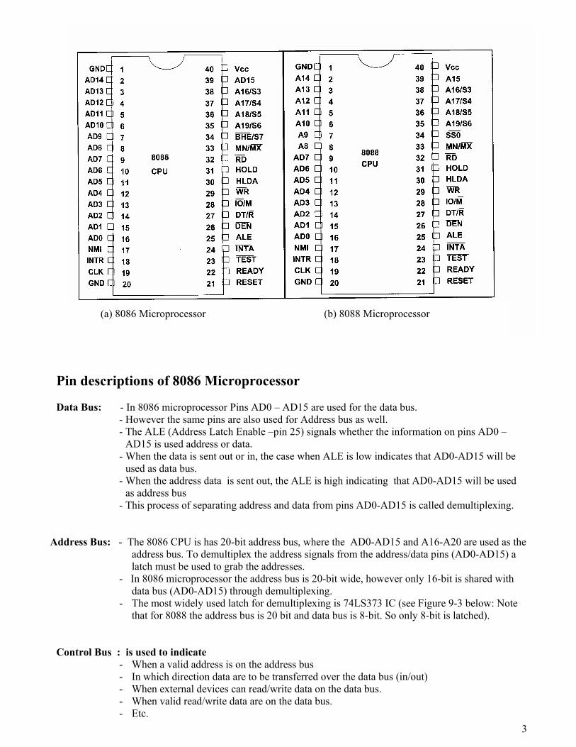
3
Pin descriptions of 8086 Microprocessor Data Bus: - In 8086 microprocessor Pins AD0 – AD15 are used for the data bus.
- However the same pins are also used for Address bus as well. - The ALE (Address Latch Enable –pin 25) signals whether the information on pins AD0 –
AD15 is used address or data. - When the data is sent out or in, the case when ALE is low indicates that AD0-AD15 will be
used as data bus. - When the address data is sent out, the ALE is high indicating that AD0-AD15 will be used
as address bus - This process of separating address and data from pins AD0-AD15 is called demultiplexing.
Address Bus: - The 8086 CPU is has 20-bit address bus, where the AD0-AD15 and A16-A20 are used as the address bus. To demultiplex the address signals from the address/data pins (AD0-AD15) a latch must be used to grab the addresses.
- In 8086 microprocessor the address bus is 20-bit wide, however only 16-bit is shared with data bus (AD0-AD15) through demultiplexing.
- The most widely used latch for demultiplexing is 74LS373 IC (see Figure 9-3 below: Note that for 8088 the address bus is 20 bit and data bus is 8-bit. So only 8-bit is latched).
Control Bus : is used to indicate
- When a valid address is on the address bus - In which direction data are to be transferred over the data bus (in/out) - When external devices can read/write data on the data bus. - When valid read/write data are on the data bus. - Etc.
(a) 8086 Microprocessor (b) 8088 Microprocessor

4
Pin Descriptions of the Control Signals of 8086 CPU
Pin Name Function 34
____ BHE (Bus High Enable)
It provides control signal to distinguish between the low byte and the high byte of the 16-bit data. (Active-low)
17
NMI (Nonmaskable Interrupt)
This signal will make the microprocessor to jump to the interrupt vector table after it finishes the current instruction. This interrupt cannot be masked by software.
18
INTR (Interrupt Request)
If it is activated, it will finish the execution of the current instruction and respond with the interrupt acknowledge operation. In IBM PC it is connected to the interrupt controller.
19 CLK (Clock) It acts as the heartbeat of the CPU. Intel has designed the 8284 clock generator and a driver to be used for the processor.
21 RESET To terminate the present activities of the microprocessor, a high signal is applied for the RESET pin.
22 READY It is an input signal used to insert a wait state for slower memories and I/O. It inserts wait states when it is low.
23
_____ TEST
This is input from the 8087 coprocessor. During execution of a wait instruction, the CPU checks this signal. If it is low, execution of the signal will continue; if not, it will stop executing.
24
_____ INTA (Interrupt acknowledge)
Active-low output signal. Informs interrupt controller that INTR has occurred and that the vector number is available on the lower 8 lines of the data bus
25 ALE (Address Latch Enable) Active-high output signal. Indicates that a valid address is available on the external address bus. See Figure 9-3.
26 ____ DEN (Data Enable)
Active-low output signal. This allows the isolation of the CPU from the system bus.
27 _ DT/R (Data transmit/receive)
Active-low output signal used to control the direction of the data flow (transmit/receive)

5
28
__ IO/M (memory or input/output)
Indicates whether the address bus is accessing memory or I/O device. In 8086, when it is high, it is accessing the memory and when it is low , it is accessing the I/O.
29 ___ WR (Write)
Active-low output signal. Indicates that the data on the data bus is being written to memory or I/O. Used along with pin 28 for write operations.
30
HLDA (hold acknowledge)
Active-high output signal. After input on HOLD, the CPU responds with HLDA to signal that DMA (Direct Memory Access) controller can use the bus.
31
HOLD (hold)
Active-high input from the DMA controller which indicates that the device is requesting access to memory and I/O space and that the CPU should release the control of the local bus.
32
___ RD (Read)
Active-low output signal. Indicates that the data on the data bus is being read from the memory or I/O. Used along with pin 28 for read operations.
Basic Busses for a computer: Every computer must have three basic busses in order to communicate: Address bus, data bus, and the control bus. The figure below shows the basic busses of 8088 based-computer. Note that the 3 control signals from 8088: WR, RD, and IO/M are used to generate 4 new control signals (MEMR, MEMW, IOR, and IOW) by using a decoder circuit.
Direct Memory Access (DMA) In computers there is often need to transfer a large amount of data between the memory and peripherals such as hard disk. In such a case using the CPU to transfer data is too slow, since the data first must be fetched into the CPU and then sent to its destination. For this reason Direct Memory Access controller is used to bypass the CPU and provide a direct connection between the peripherals and memory, thus transferring the data as fast as possible.

1
EEE 410 – Microprocessors I Spring 04/05 – Lecture Notes # 16
Outline of the Lecture • Input/Output (I/O) and Device Interfacing INPUT/OUTPUT (I/O) AND DEVICE INTERFACING
In addition to memory, 80x86 microprocessors are able to access I/O ports. Ports are accessed either to bring data from the port into the CPU (inputting) or to send data from the CPU to the port (outputting).
Input/Output Instructions in 8086 CPU
The 8086 microprocessor can access information from ports as well as from the memory. There are two instructions for this purpose “IN” and “OUT”. These instructions can send data from the accumulator (AX, AL or AH) to ports or receive data from ports into the accumulator.
Case 1: 8-bit data ports
Inputting Data Outputting Data Format IN dest,source OUT dest,source (1) IN AL,port# OUT port#,AL (2) MOV DX,port#
IN AL,DX MOV DX,port# OUT DX,AL
In format (1) above, port# is the address of the port, and can be from 00 to FFH. This 8-bit address allows 256 input ports and 256 output ports. No segment register is involved in computing the address, in contrast to the data accessed from memory. In format (2) , port# is the address of the port, and can be from 0000 to FFFFH. This 16-bit address allows 65,536 input ports and 65,536 output ports. No segment register (DS) is involved.
Ex: Write a sequence of instructions that will output FFH to a byte-wide output port at the address ABH of the I/O address space?
MOV AL,FFH OUT ABH,AL
Ex: Write a sequence of instructions that will output FFH to an output port at the address B000H of the I/O address space? MOV DX,B000H ;Note that 16-bit address must be in DX MOV AL,FFH OUT DX,AL Ex: Assume that the port address 22H is an input port for monitoring the temperature. Write Assembly language instructions to monitor the port continuously for the temperature of 100 degrees. If it reaches 100, then BH should contain ‘Y’. BACK: IN AL,22H ;get the temperature data from port# 22H CMP AL,100 ;is temp =100? JNZ BACK ;if not, keep monitoring MOV BH,’Y’ ;temp =100, load ‘Y’ into BH

2
Case 2: 16-bit data ports Inputting Data Outputting Data Format IN dest,source OUT dest,source (1) IN AX,port# OUT port#,AX (2) MOV DX,port#
IN AX,DX MOV DX,port# OUT DX,AX
Ex: Assume that AX=98F6H and the output port address is 47H, then
OUT 47H,AX
In the above case F6H, the content of AL, goes to port address 47H and 98H, the content of AH goes into the port address 48H.
In other words the low byte goes to the low port address, and the high byte goes to the high byte address.
• Types of Input / Output •
Isolated Input / Output Isolated I/O (also referred as peripheral I/O or direct I/O ) uses dedicated input (IN) and output (OUT) instructions to transfer data between the I/O device and the microprocessor. Isolated I/O uses separate map for the I/O space, freeing the entire memory for use by the program.
Memory-mapped Input / Output In memory-mapped I/O, a memory location is assigned to be input or output port, so it uses a portion of memory space for I/O transfers. This reduces the amount of memory available, but simplifies the hardware. “MOV” instruction is used instead of “IN” and “OUT” instructions. M6800, M68000 and RISC processors are examples to this type.
The 8255 programmable Peripheral Interface (PPI)
The 8255 PPI chip is designed to permit easy implementation of parallel I/O into the microcomputer. The 8255 is one of the most widely used I/O chips. It has three separately accessible ports, A, B, and C. Above all the user can program the individual ports to be input or output, and change them dynamically.
The block diagram of the 8255 Chip

3
Detailed Block Diagram of 8255 (a), and the Pin layout (b) • PA0-PA7 (Port A) : This 8-bit port can be programmed all as input or all as output or
all bits as bi-directional input/output. • PB0-PB7 (Port B) : This 8-bit port can be programmed all as input or all as output or
all bits as bi-directional port. • PC0-PC7 (Port C) : This 8-bit port can be all input or all output. It can also be split into
two parts: CU (Upper 4 bits PC4-PC7) and CL (Lower 4 bits PC0-PC3).
Each can be used for input or output.
• RD and WR : These two active low signals are inputs to the 8255. If the 8255 is using isolated I/O design, IOR or IOW of the system bus are connected to these two pins. If the port uses memory-mapped I/O, MEMR and MEMW activate them.
• RESET: This is an active high signal input to the 8255 used to clear the control register.
When RESET is activated, all ports are initialized as input ports.
• A0, A1, and CS: While CS selects the entire chip, it is A0 and A1 that select the specific port. A0 and A1 are used to access ports A, B, C, or the control register according to the table below.

4
A1 A0 Selects: 0 0 Port A 0 1 Port B 1 0 Port C 1 1 Control Register
Programming Modes of PPI 1) Mode 0: Simple input or output mode:
This mode 0 is the basic input output mode. In this mode any ports A,B or C can be programmed as input or output.
Note that in this mode a given port cannot be both input or output port at the same time.
One major characteristic of port C is that one can program CL (PC0-PC3) and CU (PC4-PC7) independent of each other.
The Control Register; is used to configure the individual ports as to be in input or output mode.
The Control Register in Mode 0 D7 D6 D5 D4 D3 D2 D1 D0
1=Mode 0 I/O Mode
Mode selection 00 = Mode 0 01 = Mode 1 1X = Mode 2
Port A 1=input 0=output
Port C (PC7-PC4) 1=input 0=output
Mode Selection 0=Mode 0 1=Mode 1
Port B 1=input 0=output
Port C (PC3-PC0) 1=input 0=output
The port Addresses for the 8255
Port Address A0 A1 A 300H 0 0 B 301H 0 1 C 302H 1 0
Control Register 303H 1 1
Ex: Configure 8255 as follows: port A as input, B as output, and all the bits in C as output. Determine the content of the Control Register and, Program the ports to input data from A and send it to both B and C.
(Assume the standard port addresses of 8255 given above) Soln: a) Control register:
1 0 0 1 0 0 0 0 b) MOV AL,90H ; This control byte is used to initialize the PPI MOV DX,303H ;get the address of Control Register OUT DX,AL ;output the Control Byte to the Control register MOV DX,300H ;get the address of Port A IN AL,DX ;input data from Port A MOV DX,301H ;get the address of Port B OUT DX,AL ;output data to Port B MOV DX,302H ;get the address of Port C OUT DX,AL ;output data to Port C
Note that first two bits of the Address are used for the mode selection as shown in the table given above.
Table 1:
= 90H

5
Ex: Configure the ports of 8255 as follows: port A=input, B=output/ PC0 –PC3=input, and PC4-PC7=output. Determine the content of the Control Register and, Program the 8255 to get data from port A and send it to port B. In addition, input data from PCL and send out to PCU. (PCL=Lower 4 bits (nibble) of Port C, PCU;Upper 4 bits(nibble) of Port C). (Assume the standard port addresses of 8255 given above) Soln: a) Control register:
1 0 0 1 0 0 0 1 b) MOV AL,91H ; This control byte is used to initialize the PPI MOV DX,303H ;get the address of Control Register OUT DX,AL ;output the Control Byte to the Control register MOV DX,300H ;get the address of Port A IN AL,DX ;input data from Port A MOV DX,301H ;get the address of Port B OUT DX,AL ;output data to Port B MOV DX,302H ;get the address of Port C IN AL,DX ;get the data from Port C
AND AL,0FH ;mask the upper bits MOV CL,4 ;rotate count =4 ROL AL,CL ;shift the bits to upper position OUT DX,AL ;output PCL to PCU
2) Mode 1: I/O with handshaking capability: One of the most powerful features of the 8255 is the ability to handle handshaking
signals. Handshaking refers to the process of communicating back and forth between two intelligent devices. Printer is a good example for Mode 1 Interfacing.
Port A and B are used for input or output while Port C is used for handshaking signals.
3) Mode 2: Bi-directional I/O with handshaking:
In this mode data is transferred both in and out via the same port with handshaking capability. Port A is used as a bi-directional port and port C is used for handshaking signals. Port B can be configured to be in Mode 0 or 1.
= 91H
1
EEE 410 – Microprocessors I Spring 04/05 – Lecture Notes # 17
Outline of the Lecture • I/O Programming in Assembly Language PROGRAMMING THE PPI (MODE 0) Ex: Configure the ports of 8255 (PPI) as follows: port A=input,
port B=output, port CH=output, port CL=input
(CL=Lower 4 bits of Port C, CH (CU) =Upper 4 bits of Port C) (Assume that the 8255 PPI is located at 300H) Soln: Control register: A CH B CL
1 0 0 0 1 : input 0 : output A CH B CL
1 0 0 1 0 0 0 1
;This program initializes the PPI located at 300H as follows: ; port A : input ; port B : output ; port CH : output ; port CL : input .MODEL SMALL .CODE MAIN: MOV AL,10010001B MOV DX,303H ;If PPI is at 300H, then Port A=300H,
OUT DX,AL ;Port B =301, Port C=302 and Control reg:303H … … … MOV AH,4CH INT 21H END MAIN

2
I/O INTERFACE APPLICATIONS Application 1: Stepper Motor Control
Stepper motors are used for position control applications, such as for the control of the disk drives and in robotics. • The most common stepper motors have four stator windings that are paired with a
center tapped common shown in Figure below (Figure 12.38-39 of the textbook). • While the conventional motor shaft runs freely, the stepper motor shaft moves in a fixed
repeatable increment, which allows one to move it to a precise position.
Figure 12-38. Rotor alignment of the stepper motor.
Figure 12-38. Stator windings configuration
• The table below shows a normal 4-step Sequence. Note that once, we start with any of
the sequences in Table below (i.e. step 3 [0110] ) we must continue in the sequence of steps, 4, 1, 2, and so on.
Step # Winding A Winding B Winding C Winding D 1 1 0 0 1 2 1 1 0 0 3 0 1 1 0
Clockwise | | |
\ / 4 0 0 1 1
Counter Clockwise
/ \ | |
Normal 4-Step Sequence

3
Figure 12-40:8255 Connection to Stepper Motor Ex: Given the 8255 connection to the stepper motor of Figure 12-40,
- code a program to rotate it continuously. - press any key on the IBM PC keyboard to stop it.
(Assume that the 8255 PPI is located at 300H) Use Port A as the output port, then the Control register will contain: A CH B CL
1 0 0 0 1 : input 0 : output A CH B CL
1 0 0 0 0 0 0 0 ………… MOV AL,80H ;control word for all 8255 ports as out MOV DX,303H ;control register address of 8255 OUT DX,AL ;to control register MOV BL,66H ;or BL=33H, BL=99H or BL=0CCH AGAIN: MOV AH,01 ;check the key press INT 16H ;using INT 16
JNZ EXIT ;stop if any key pressed MOV AL,BL ;otherwise send pulse to the stepper motor MOV DX,300H ;port A address of 8255 OUT DX,AL MOV CX,0FFFFH ;(change this value to see rotation speed)
HERE: SUB AH,AH LOOP HERE ;wait for delay
ROR BL,1 ;rotate for the next step JMP AGAIN ;and continue until a key is pressed

4
EXIT: Application 2: 7 Segment Display Control
This program displays 5 hexadecimal digits on the 7-segment LED display units connected to the 8255 PPI as shown above. ;------ data segment ------ .DATA MSG DB 0EH,0EH,4,1,1 ;------ code segment ------ .CODE MAIN: MOV AX,@DATA MOV DS,AX MOV DX,303H MOV AL,10000000B OUT DX,AL START: MOV SI,OFFSET MSG
MOV DI,0 MOV BL,00010000B NEXT: MOV BH,[SI+DI] CALL DISPLAY ;CALL THE DISPLAY SUBROUTINE SHR BL,1 INC DI CMP DI,4 JNE NEXT JMP START DISPLAY: MOV DX,300H ;DISPLAY SUBROUTINE MOV AL,BL OUT DX,AL MOV DX,301H MOV AL,BH OUT DX,AL RET END MAIN
7-Segment LED Display Driver Circuit

5
Application 3: Keyboard Control
This program reads a keystroke from the 64-key keyboard connected to the PPI as shown above. (The program ignores the debounce effect) ;------ data segment ------ .DATA LETTERS DB ‘0123456789ABCDEFGHIJKLMNOPRSTUVWXYZabcdefghijklmnopqrstuvwxyz.?’ ;------ code segment ------ .CODE MAIN: MOV AX,@DATA MOV DS,AX MOV DX,303H MOV AL,10000010B OUT DX,AL
MOV BL,11111110B SCAN: ROR BL
MOV AL,BL MOV DX,300H OUT DX,AL CMP AL,11111111B JE SCAN PUSH BX MOV DI,0
NEXT: SHL BL,1 JNC FINISHC INC DI JMP NEXT
FINISHC: SHL AL,1 JNC FINISHR ADD DI,8 JMP NEXT
FINISHR: MOV SI,OFFSET LETTERS MOV DL,[SI+DI]
MOV AH,2 INT 21H
POP BX JMP SCAN END MAIN

1
EEE 410 – Microprocessors I Spring 04/05 – Lecture Notes # 18
Outline of the Lecture • Interfacing the Parallel Port
♦ Standard Parallel Port (SPP) ♦ Port addresses ♦ Software registers and programming ♦ Bi-directional ports ♦ Using parallel port’s IRQ ♦ Enhanced Parallel Port (EPP) ♦ Extended Capabilities Port (ECP)
• Standard Parallel Port
The Parallel Port is the most commonly used port for interfacing. This port will allow the input of up to 9 bits or the output of 12 bits at any one given time, thus requiring minimal external circuitry to implement many simpler tasks.
It's found commonly on the back of your PC as a D-Type 25 Pin female connector. Parallel Port’s are standardized under the IEEE 1284 standard first released in 1994. This standard defines 5 modes of operation which are as follows,
1. Compatibility Mode. (Centronics Mode) 2. Nibble Mode. 3. Byte Mode. 4. EPP Mode (Enhanced Parallel Port). 5. ECP Mode (Extended Capabilities Mode).
Compatibility mode is also known as "Centronics Mode". In this mode you can only
output data. To receive/input data, you must change the mode to either Nibble or Byte mode.
Nibble mode can input a nibble (4 bits) from device to computer. Byte mode uses the Parallel's bi-directional feature (found only on some cards) to
input a byte (8 bits) of data. Extended and Enhanced Parallel Ports use additional hardware to generate and
manage handshaking. For example, to output a byte to a printer (or anything in that matter) using compatibility
mode, the software must,
1. Write the byte to the Data Port. 2. Check to see is the printer is busy. If the printer is busy, it will not accept any data, thus any data which is written will be lost. 3. Take the Strobe (Pin 1) low. This tells the printer that there is the correct data on the data lines/pins (Pins 2-9). 4. Put the strobe high again after waiting approximately 5 microseconds after putting the strobe low. (Step 3)
This limits the speed at which the port can run at. The EPP & ECP ports get around
this by letting the hardware check to see if the printer is busy and generate a strobe and /or appropriate handshaking. This means only one I/O instruction need to be performed, thus increasing the speed. These ports can output at around 1-2

2
megabytes per second. The ECP port also has the advantage of using DMA channels and FIFO buffers, thus data can be shifted around without using I/O instructions.
• Port Addresses The Parallel Port has three commonly used base addresses. LPT1 is normally assigned base address 378h, while LPT2 is assigned 278h. 378h & 278h have always been commonly used for Parallel Ports.
Address Notes:
3BCH - 3BFH Used for Parallel Ports which were incorporated on to Video Cards - Doesn't support ECP addresses
378H - 37FH Usual Address For LPT 1 278H - 27FH Usual Address For LPT 2
Table 2 Port Addresses • Hardware Properties
Below is a table of the "Pin Outs" of the D-Type 25 Pin connector and the Centronics 34 Pin connector. The D-Type 25 pin connector is the most common connector found on the Parallel Port of the computer, while the Centronics Connector is commonly found on printers.
Pin No (D-Type 25)
Pin No (Centronics) SPP Signal Direction
In/out Register Hardware Inverted
1 1 NStrobe In/Out Control Yes 2 2 Data 0 Out Data 3 3 Data 1 Out Data 4 4 Data 2 Out Data 5 5 Data 3 Out Data 6 6 Data 4 Out Data 7 7 Data 5 Out Data 8 8 Data 6 Out Data 9 9 Data 7 Out Data 10 10 nAck In Status 11 11 Busy In Status Yes
12 12 Paper-Out / Paper-End In Status
13 13 Select In Status 14 14 NAuto-Linefeed In/Out Control Yes 15 32 NError / nFault In Status 16 31 NInitialize In/Out Control
17 36 NSelect-Printer / nSelect-In In/Out Control Yes
18 - 25 19-30 Ground Gnd
Table 1. Pin Assignments of the D-Type 25 pin Parallel Port Connector.

3
The above table uses "n" in front of the signal name to denote that the signal is active
low. e.g. nError. If the printer has occurred error then this line is low.
The "Hardware Inverted" means the signal is inverted by the Parallel card's hardware. Such an example is the Busy line. If +5v (Logic 1) was applied to this pin and the status register read, it would return back a 0 in Bit 7 of the Status Register.
The output of the Parallel Port is normally TTL logic levels. The voltage levels are the
easy part. The current you can sink and source varies from port to port. Most Parallel Ports can sink and source around 12mA. The best way is to use a buffer, so the least current is drawn from the Parallel Port.
• Centronics?
Centronics is an early standard for transferring data from a host to the printer. The majority of printers use this handshake. This handshake is normally implemented using a Standard Parallel Port under software control.
• Software Registers - Standard Parallel Port (SPP)
Offset Name Read/Write Bit No. Properties Bit 7 Data 7 Bit 6 Data 6 Bit 5 Data 5 Bit 4 Data 4 Bit 3 Data 3 Bit 2 Data 2 Bit 1 Data 1
Base + 0 Data Port/ Data Register
Write (Note-1)
Bit 0 Data 0
Table 4 Data Port
Note 1 : If the Port is Bi-Directional then Read and Write Operations can be performed on the Data Register.
The base address, usually called the Data Port or Data Register is simply used for outputting data on the Parallel Port's data lines (Pins 2-9). This register is normally a write only port. If you read from the port, you should get the last byte sent. However if your port is bi-directional, you can receive data on this address.

4
Offset Name Read/Write Bit No. Properties
Bit 7 Busy Bit 6 Ack Bit 5 Paper Out Bit 4 Select In Bit 3 Error Bit 2 IRQ (Not) Bit 1 Reserved
Base + 1 Status Port/Status
Register
Read Only
Bit 0 Reserved
Table 5 Status Port
The Status Port (base address + 1) is a read only port. Any data written to this port will be ignored. The Status Port is made up of 5 input lines (Pins 10,11,12,13 & 15), an IRQ status register and two reserved bits.
Offset Name Read/Write Bit No. Properties Bit 7 Unused Bit 6 Unused Bit 5 Enable Bi-Directional PortBit 4 Enable IRQ Via Ack LineBit 3 Select Printer Bit 2 Initialize Printer (Reset) Bit 1 Auto Linefeed
Base + 2 Control Port/ Control Register
Read/Write
Bit 0 Strobe
Table 6 Control Port
The Control Port (base address + 2) was intended as a write only port. When a printer is attached to the Parallel Port, four "controls" are used. These are Strobe, Auto Linefeed, Initialize and Select Printer, all of which are inverted except Initialize.
• Bi-directional Ports
Bit 5 of the Control Port enables or disables the bi-directional function of the Parallel Port. This is only available on true bi-directional ports. When this bit is set to one, pins 2 to 9 go into high impedance state. Once in this state you can enter data on these lines and retrieve it from the Data Port (base address). Any data which is written to the data port will be stored but will not be available at the data pins. To turn off bi-directional mode, set bit 5 of the Control Port to '0'.
However not all ports behave in the same way. Other ports may require setting bit 6 of the Control Port to enable Bi-directional mode and setting of Bit 5 to dis-enable Bi-directional mode, Different manufacturers implement their bi-directional ports in different ways. If you wish to use your Bi-directional port to input data, test it with a logic probe or multimeter first to make sure it is in bi-directional mode.

5
• Using The Parallel Port to Input 8 Bits.
If your Parallel Port doesn't support bi-directional mode, don't despair. You can input a maximum of 9 bits at any one given time. To do this you can use the 5 input lines of the Status Port and the 4 inputs (open collector) lines of the Control Port.
In order to input 8-bit input data we input data both from status port and control port.
The high nibble of status port and low nibble of the control port are combined to make an 8-bit input data.
• Using the Parallel Port's IRQ
The Parallel Port's interrupt request is not used for printing under DOS or Windows. Early versions of OS-2 used them, but don't anymore. Interrupts are good when interfacing monitoring devices such as high temp alarms etc, where you don't know when it is going to be activated. It's more efficient to have an interrupt request rather than have the software poll the ports regularly to see if something has changed. This is even more noticeable if you are using your computer for other tasks, such as with a multitasking operating system.
The Parallel Port's interrupt request is normally IRQ5 or IRQ7 but may be something else if these are in use. It may also be possible that the interrupts are totally disabled on the card, if the card was only used for printing.
The Parallel Port interrupt can be disabled and enabled using bit 4 of the control register, Enable IRQ Via Ack Line. Once enabled, an interrupt will occur upon a low to high transition (rising edge) of the nACK. However like always, some cards may trigger the interrupt on the high to low transition.
You must program the programmable interrupt controller (PIC) at address 020H to respond to the interrupt you are using and then place an Interrupt Service Routine (ISR) at the appropriate Interrupt Vector.

6
• Programming of the Parallel Port Ex1: Write required Assembly Language instructions to output 11111111B to the Data Port of the SPP?
MOV DX,378H ;base address of SPP is 378H MOV AL,11111111B ;Data Port is placed at [base address + 0] OUT DX,AL
Ex2: Write required Assembly Language instructions to check if the Paper has run out at the printer (paper out).
Bit 5 of the Status port indicates the status of paper at the Printer. So after inputting 8-bit data from this port at [base address+1] we can check if paper is finished or not.
MOV DX,378H ;base address of SPP is 378H
INC DX ;[378H+1] IN AL,DX AND AL,00100000B CMP AL,00100000B JE OVER CALL PAPER_OK ;a procedure to report that paper is ok! JMP OVER2
OVER: CALL PAPER_OUT ;a procedure to report that paper is run out OVER2:
• EPP - Enhanced Parallel Port The Enhanced Parallel Port (EPP) was designed in a joint venture between Intel,
Xircom & Zenith Data Systems. EPP Ports were first specified in the EPP 1.7 standard, and then later included in the IEEE 1284 Standard released in 1994. EPP has two standards, EPP 1.7 and EPP 1.9. There are differences between the two standards which may affect the operation of devices. This is further discussed latter. EPP has a typical transfer rate in the order of 500KB/S to 2MB/S. This is achieved by allowing the hardware contained in the port to generate handshaking, strobing etc, rather that have the software do it, which was the case with Centronics.
EPP is more commonly used than ECP. EPP differs from ECP by the fact that the EPP Port generates and controls all the transfers to and from the peripheral. ECP on the other hand requires the peripheral to negotiate a reverse channel and control the handshaking. This is harder to achieve, thus really requires a dedicated controller or ECP Peripheral Chip.
• (ECP) Extended Capabilities Port The Extended Capabilities Mode was designed by Hewlett Packard and Microsoft to
be implemented as the Extended Capabilities Port Protocol and ISA Interface Standard. This protocol uses additional hardware to generate handshaking signals etc just like the EPP mode, thus runs at very much the same speed than the EPP mode. This mode, however may work better under Windows as it can use DMA

7
channels to move it's data about. It also uses a FIFO buffer for the sending and/or receiving of data.
Another feature of ECP is a real time data compression. It uses Run Length Encoding (RLE) to achieve data compression ratio's up to 64:1. This comes is useful with devices such as Scanners and Printers where a good part of the data is long strings which are repetitive.
The Extended Capabilities Port supports a method of channel addressing. This is not intended to be used to daisy chain devices up but rather to address multiple devices within one device. Such an example is many fax machines on the market today which may contain a Parallel Port to interface it to your computer. The fax machine can be split up into separate devices such as the scanner, modem/Fax and printer, where each part can be addresses separately, even if the other devices cannot accept data due to full buffers.
REFENENCE:
Read, http://www.beyondlogic.org/spp/parallel.htm ,for further details.
HOMEWORK: Write a subroutine to send a character to a printer using Standard Parallel Port (SPP) communication. The subroutine will assume that the character is stored in AL.

1
EEE 410 – Microprocessors I Spring 04/05 – Lecture Notes # 19
Outline of the Lecture • Interfacing the Serial Port • Basics of Serial Communication • Asynchronous Data Communication and Data Framing • RS232 and other Serial I/O Standards BASICS OF SERIAL COMMUNICATION
Computers transfer data in two ways: parallel and serial.
• Parallel communication is fast and efficient. In parallel communication 8 or more lines (wire conductors) are used to transfer data to a device that only a few feet away. (e.g. printers, hard disks etc.)
• Parallel communication provides much faster transfer of data with compared to serial communication.
• However for long distances the number of wires required as well as the distortion on the signals in parallel wires makes parallel communication for long distances not reliable. Also the synchronization of the parallel signals is a big problem.
• Serial communication sends 1 bit at a time, so it is slower with compared to parallel communication.
• For long distances serial communication provides robust way of data transfer. Because there is no problem of synchronization.
• Serial communication requires less number of wires for communication. Serial communication is used in modems, keyboards etc.
Serial versus Parallel Data transfer. Asynchronous /Synchronous Methods
Serial data communication uses two methods: asynchronous and synchronous. • Synchronous communication requires common timing signals and common
clock for synchronization. This means that as well as the data, the clock signals must also be transmitted along. In synchronous method a block of data at a time is transmitted.
• In asynchronous method a single byte is transferred at a time. For example, start and stop bits are used to indicate the receipt of a byte.
Serial Data Transfer Parallel Transfer
Sender Receiver Sender
Receiver
D0
D7

2
Serial Data Communication Systems
• Simplex Transmission: Transmission of data is only possible in one direction (e.g. output only-printers)
• Half Duplex Transmission: Transmission of data is possible in both directions, but in one direction at a time.
• Full Duplex Transmission: Transmission of data can be in both directions at a time. Requires to wires as data lines.
Simplex, Half and Full Duplex Transfers
UART (Universal Asynchronous Receiver-Transmitter) Chip UART chips are used for serial communication. The 8250 series, which includes the 16450, 16550, 16650, & 16750 UARTS, are the most commonly used. • Asynchronous serial communication and data framing
The data coming in the receiving end of the data line in a serial data transfer is all 1s and 0s; it is difficult to make sense of data unless the sender and receiver agree on a set of rules, a protocol on how the data is packed, how many bits constitute a character, and when the data begins and ends.
Start and Stop bits
Asynchronous serial data communication is widely used for character-oriented transmission, and block-oriented data transfers use the Synchronous method.
Simplex Transmitter Receiver
Half Duplex
Transmitter Receiver
Receiver Transmitter
Full Duplex
Transmitter Receiver
Receiver Transmitter

3
In the Asynchronous method, each character is put between a start and stop bits. This is called framing. In data framing, for asynchronous communications, the data such as ASCII characters are packed in between a start bit and stop bit. The start bit is always one bit, but the stop bit(s) can be one or two bits. The start bit is always a 0 (low) and the stop bit(s) is 1 (high) The example below gives the framing of the ASCII character “A”, where, binary 0100 0001, is framed in between the start bit and two stop bits. Notice that the LSB is sent out first.
Framing of ASCII “A” (41H)
Notice that the transmission begins with a start bit followed by D0, the LSB, then the rest of the bits until the MSB (D7), and finally, the 2 stop bits indicating the end of character “A”.
In asynchronous serial communication, peripheral chips and modems can be programmed for data that is 5, 6, 7 or 8 bits wide.
In some systems in order to maintain the data integrity, the parity bit of the character byte is included in the data frame.
Data Transfer Rate (Baud Rate)
The rate of data transfer in serial communication is stated in bps (bits per second). Another widely used terminology for bps is the baud rate.
Typical bps values are: 2,400, 4,800, 9,600, 19,200, 28,800,… etc.
• RS232 and other Serial I/O Standards RS232 is the most widely used serial I/O interfacing standard. However the I/O voltage levels are not TTL compatible. In the RS232 a 1 is
represented by –3 to –25 V, while 0 bit is +3 to +25 V, making –3 to +3 undefined. For this reason voltage converter such as MC1488 and MC1489 are used to
convert the TTL logic levels to the RS232 voltage levels and vice versa. See Figure below.

4
RS232 Pins
Serial Ports come in two "sizes". There are the D-Type 25 pin connector and the D-Type 9 pin connector both of which are male on the back of the PC, thus you will require a female connector on your device. Below is a table of pin connections for the 9 pin and 25 pin D-Type connectors.
D-Type 25 pin D-Type 9-pin
Serial Port Pinouts (D25 and D9 Connectors)
D-Type-25 Pin No.
D-Type-9 Pin No. Abbreviation Full Name
Pin 2 Pin 3 TD / TxD Transmit Data Pin 3 Pin 2 RD / (RxD) Receive Data Pin 4 Pin 7 RTS Request To Send Pin 5 Pin 8 CTS Clear To Send Pin 6 Pin 6 DSR Data Set Ready Pin 7 Pin 5 SG / (GND) Signal Ground Pin 8 Pin 1 CD / (DCD) Data Carrier Detect
Pin 20 Pin 4 DTR Data Terminal Ready
Pin 22 Pin 9 RI Ring Indicator Table 1 : D Type 9 Pin and D Type 25 Pin Connectors

5
Pin Functions
Abbreviation Full Name Function
TD Transmit Data Serial Data Output (TXD)
RD Receive Data Serial Data Input (RXD)
CTS Clear to Send This line indicates that the Modem is ready to exchange data.
DCD Data Carrier
Detect When the modem detects a "Carrier" from the modem at the other end of the phone line, this Line becomes active.
DSR Data Set Ready
This tells the UART that the modem is ready to establish a link.
DTR Data
Terminal Ready
This is the opposite to DSR. This tells the Modem that the UART is ready to link.
RTS Request To Send
This line informs the Modem that the UART is ready to exchange data.
RI Ring Indicator Goes active when modem detects a ringing signal.
Data Communication Classification:
Devices which use serial cables for their communication are split into two categories. These are DCE (Data Communications Equipment) and DTE (Data Terminal Equipment.)
DTE refers to terminals and computers that send and receive data; DCE refers to communication equipment such as modems that are responsible for transferring data.

1
EEE 410 – Microprocessors I Spring 04/05 – Lecture Notes # 20
Outline of the Lecture • Interfacing the Serial Port
• Serial Port registers • Transmitting Serial Data • Receiving Serial Data
INTERFACING THE SERIAL PORT • Serial Port’s Registers (PC’s)
Port Addresses & IRQ's Name Address IRQ COM 1 3F8 4 COM 2 2F8 3 COM 3 3E8 4 COM 4 2E8 3
Table : Standard Port Addresses
Above is the standard port addresses. These should work for most P.C's. However some PCs can have different set of addresses and IRQ's. Just like the LPT ports, the base addresses for the COM ports can be read from the BIOS Data Area.
Start Address Function 0000:0400 COM1's Base Address 0000:0402 COM2's Base Address 0000:0404 COM3's Base Address 0000:0406 COM4's Base Address
Table - COM Port Addresses in the BIOS Data Area; The above table shows the address at which we can find the Communications
(COM) ports addresses in the BIOS Data Area.
Table of Registers of UART Base Address DLAB Read/Write Abr. Register Name
=0 Write - Transmitter Holding Buffer =0 Read - Receiver Buffer + 0 =1 Read/Write - Divisor Latch Low Byte =0 Read/Write IER Interrupt Enable Register + 1 =1 Read/Write - Divisor Latch High Byte - Read IIR Interrupt Identification Register + 2 - Write FCR FIFO Control Register
+ 3 - Read/Write LCR Line Control Register + 4 - Read/Write MCR Modem Control Register + 5 - Read LSR Line Status Register + 6 - Read MSR Modem Status Register
+ 7 - Read/Write - Scratch Register
Table : Table of Registers

2
DLAB ?
• You will have noticed in the table of registers that there is a DLAB column. When DLAB is set to '0' or '1' some of the registers change. This is how the UART is able to have 12 registers (including the scratch register) through only 8 port addresses.
• DLAB stands for Divisor Latch Access Bit. When DLAB is set to '1' via the
line control register, two registers become available from which you can set your speed of communications measured in bits per second.
• The UART will have a crystal which should oscillate around 1.8432 MHZ. The
UART incorporates a divide by 16 counter which simply divides the incoming clock signal by 16. Assuming we had the 1.8432 MHZ clock signal, that would leave us with a maximum, 115,200 hertz signal making the UART capable of transmitting and receiving at 115,200 Bits Per Second (BPS). That would be fine for some of the faster modems and devices which can handle that speed, but others just wouldn't communicate at all. Therefore the UART is fitted with a Programmable Baud Rate Generator which is controlled by two registers.
• Ex: Lets say for example we only wanted to communicate at 2400 BPS??
We would have to divide 115,200 by 48 to get a workable 2400 Hertz Clock.
The "Divisor", in this case 48, is stored in the two registers controlled by the "Divisor Latch Access Bit". This divisor can be any number, which can be stored in 16 bits (ie 0 to 65535). The UART only has a 8 bit data bus, thus this is where the two registers are used. The first register (Base + 0) when DLAB = 1 stores the "Divisor latch low byte" where as the second register (base + 1 when DLAB = 1) stores the "Divisor latch high byte."
Below is a table of some more common speeds and their divisor latch high bytes & low bytes. Note that all the divisors are shown in Hexadecimal.
Speed (BPS) Divisor (Dec) Divisor Latch High Byte Divisor Latch Low Byte 50 2304 09h 00h 300 384 01h 80h 600 192 00h C0h 2400 48 00h 30h 4800 24 00h 18h 9600 12 00h 0Ch
19200 6 00h 06h 38400 3 00h 03h 57600 2 00h 02h 115200 1 00h 01h
Table : Table of Commonly Used Baudrate Divisors

3
Line Control Register (LCR)
• The Line Control register sets the basic parameters for communication. Bit 7 is the Divisor Latch Access Bit or DLAB for short. We have already talked about what it does. Bit 6 Sets break enable. When active, the TD line goes into "Spacing" state which causes a break in the receiving UART. Setting this bit to '0' Disables the Break.
1 Divisor Latch Access Bit Bit 7
0 Access to Receiver buffer, Transmitter buffer & Interrupt Enable Register
Bit 6 Set Break Enable Bit 5 Bit 4 Bit 3 Parity Select
X X 0 No Parity 0 0 1 Odd Parity 0 1 1 Even Parity 1 0 1 High Parity (Sticky)
Bits 3, 4 and 5
1 1 1 Low Parity (Sticky) Length of Stop Bit
0 One Stop Bit Bit 2
1 2 Stop bits for words of length 6,7 or 8 bits or 1.5 Stop Bits for Word lengths of 5 bits.
Bit 1 Bit 0 Word Length 0 0 5 Bits 0 1 6 Bits 1 0 7 Bits
Bits 0 and 1
1 1 8 Bits Table: Line Control Register
• Bits 3,4 and 5 select parity. If you study the 3 bits, you will find that bit 3 controls
parity. That is, if it is set to '0' then no parity is used, but if it is set to '1' then parity is used. Jumping to bit 5, we can see that it controls sticky parity. Sticky parity is simply when the parity bit is always transmitted and checked as a '1' or '0'. This has very little success in checking for errors as if the first 4 bits contain errors but the sticky parity bit contains the appropriately set bit, then a parity error will not result. Sticky high parity is the use of a '1' for the parity bit, while the opposite, sticky low parity is the use of a '0' for the parity bit.
• If bit 5 controls sticky parity, then turning this bit off must produce normal parity
provided bit 3 is still set to '1'. Odd parity is when the parity bit is transmitted as a '1' or '0' so that there is a odd number of 1's. Even parity must then be the parity bit produces and even number of 1's.
• Bit 2 sets the length of the stop bits. Setting this bit to '0' will produce one stop bit,
however setting it to '1' will produce either 1.5 or 2 stop bits depending upon the word length. Note that the receiver only checks the first stop bit.
• Bits 0 and 1 set the word length. This should be pretty straight forward. A word length
of 8 bits is most commonly used today.
/Mark /Space

4
Modem Control Register (MCR)
Bit Notes Bit 7 Reserved Bit 6 Reserved Bit 5 Autoflow Control Enabled (16750 only) Bit 4 LoopBack Mode Bit 3 Aux Output 2 Bit 2 Aux Output 1 Bit 1 Force Request to Send Bit 0 Force Data Terminal Ready
Table: Modem Control Register • The Modem Control Register is a Read/Write Register. Bits 5,6 and 7 are reserved. Bit
4 activates the loopback mode. In Loopback mode the transmitter serial output is placed into marking state. The receiver serial input is disconnected. The transmitter out is looped back to the receiver in. DSR, CTS, RI & DCD are disconnected. DTR, RTS, OUT1 & OUT2 are connected to the modem control inputs. The modem control output pins are then place in an inactive state. In this mode any data which is placed in the transmitter registers for output is received by the receiver circuitry on the same chip and is available at the receiver buffer. This can be used to test the UARTs operation.
• Aux Output 2 maybe connected to external circuitry which controls the UART-CPU
interrupt process. Aux Output 1 is normally disconnected, but on some cards is used to switch between a 1.8432MHZ crystal to a 4MHZ crystal which is used for MIDI. Bits 0 and 1 simply control their relevant data lines. For example setting bit 1 to '1' makes the request to send line active.
Line Status Register (LSR)
Bit Notes Bit 7 Error in Received FIFO Bit 6 Empty Data Holding Registers Bit 5 Empty Transmitter Holding Register Bit 4 Break Interrupt Bit 3 Framing Error Bit 2 Parity Error Bit 1 Overrun Error Bit 0 Data Ready
Table : Line Status Register • The line status register is a read only register. Bit 7 is the error in received FIFO bit.
This bit is high when at least one break, parity or framing error has occurred on a byte, which is contained in the FIFO.
• When bit 6 is set, both the transmitter holding register and the shift register are
empty. The UART's holding register holds the next byte of data to be sent in parallel

5
fashion. The shift register is used to convert the byte to serial, so that it can be transmitted over one line.
• When bit 5 is set, only the transmitter holding register is empty. So what's the
difference between the two? When bit 6, the transmitter holding and shift registers are empty, no serial conversions are taking place so there should be no activity on the transmit data line. When bit 5 is set, the transmitter holding register is empty, thus another byte can be sent to the data port, but a serial conversion using the shift register may be taking place.
• The break interrupt (Bit 4) occurs when the received data line is held in a logic state '0'
(Space) for more than the time it takes to send a full word. That includes the time for the start bit, data bits, parity bits and stop bits.
• A framing error (Bit 3) occurs when the last bit is not a stop bit. This may occur due to a
timing error. You will most commonly encounter a framing error when using a null modem linking two computers or a protocol analyzer when the speed at which the data is being sent is different to that of what you have the UART set to receive it at.
• A overrun error normally occurs when your program can't read from the port fast
enough. If you don't get an incoming byte out of the register fast enough, and another byte just happens to be received, then the last byte will be lost and a overrun error will result.
• Bit 0 shows data ready, which means that a byte has been received by the UART and
is at the receiver buffer ready to be read.
Modem Status Register (MSR)
Bit Notes
Bit 7 Carrier Detect Bit 6 Ring Indicator Bit 5 Data Set Ready Bit 4 Clear To Send Bit 3 Delta Data Carrier Detect Bit 2 Trailing Edge Ring Indicator Bit 1 Delta Data Set Ready Bit 0 Delta Clear to Send
Table: Modem Status Register
• Bit 0 of the modem status register shows delta clear to send, delta meaning a change in, thus delta clear to send means that there was a change in the clear to send line, since the last read of this register. This is the same for bits 1 and 3.
• Bit 1 shows a change in the Data Set Ready line where as Bit 3 shows a change in the
Data Carrier Detect line. Bit 2 is the Trailing Edge Ring Indicator which indicates that there was a transformation from low to high state on the Ring Indicator line.

6
• Bits 4 to 7 show the current state of the data lines when read. Bit 7 shows Carrier Detect, Bit 6 shows Ring Indicator, Bit 5 shows Data Set Ready & Bit 4 shows the status of the Clear To Send line.
Example Questions: Ex1: Write the required assembly Language program segment to provide the following frame for serial communication? - 7 bits character, 1 stop bit, odd parity Solution: We can provide the above settings by using the Line Control Register. D7 D6 D5 D4 D3 D2 D1 D0 DLAB Break Parity2 Parity1 Parity0 Stop Data1 Data0
Then, 0000 1010B = 0AH is to be sent to the address of the Line Control Register (base +03H) MOV DX,3FBH ;3F8H+03 MOV AL,0AH ;the control data OUT DX,AL ;issue the control data Ex2: Program the divisor latch to provide 9600 baud rate. Assume 1.8432 MHz frequency.
16..
×=
ratebaudfreqclockrefvalueDivisor
Divisor value = 1.8432 x 10⁶/(9600 x 16)= 115200/9600=12 Then D7 of the Line Control register must be 1 for accessing DLAB. MOV AL,80H ;10000000B to access DLAB MOV DX,3FBH ; the address of the control register (3F8H+03) OUT DX,AL ;make D7=1 for DLAB ;now send the divisor value MOV AL,12 ;9600 baud rate MOV DX,3F8H ; Low byte divisor latch address
00 =5 data bits 01 =6 data bits 10 =7 data bits 11 =8 data bits
0=1 stop bits 1=2 stop bits
XX0 = No parity 001 = Odd parity 011 = Even parity 101 =High parity(sticky) 111=Low parity(sticky)
0=break 1=disable break
1 = Divisor Latch Access Bit 0 = Access to receiver/ Transmitter buffer

7
OUT DX,AL ;issue the low byte MOV AL,00 INC DX ;high byte divisor latch address(3F8H+01) OUT DX,AL
• Transmitting Serial data The following procedure is used to transmit serial data using the Serial port.
1. set DTR & RTS (DTR-Data Terminal Ready & RTS-Request To Send) (write 0000 0011B to the Modem Control register at base address+04 ) 2. check DSR & CTS (DSR-Data Set Ready & CTS-Clear to send)
(check if bits 5 & 4 in the Modem Status register are equal to 1 at base address+06) wait until timeout
3. check if Transmitter Holding Register (bit 5 of Line Status register) is Empty
(empty means ready for a byte/ is bit 5 is equal to1 at base address+5) wait until timeout
4. write the byte to data register (Transmitter Holding Buffer) (Transmitter holding buffer is at base address+00/ the parallel data in
transmitter holding buffer is transferred into transmit shift register to provide serial transmit)
• Receiving Serial Data The following procedure is used to receive serial data using the Serial port.
1. set DTR (DTR-Data Terminal Ready) (write 0000 0001B to the Modem Control register) 2. check DSR (DSR-Data Set Ready)
(check if bits 5 of the Modem Status Register) wait until timeout
3. check if Data is Ready (bit 0 of Line Status Register) (Data ready means that data has been received and is at the receiver buffer to be read)
wait until timeout 4. read the byte from data register (Receiver Buffer) (Receiver Buffer is at the base address+00)
REFERENCE:
Read, http://www.beyondlogic.org/serial/serial1.htm for further details.