effect of high carbon incorporation in co substrates on
TRANSCRIPT

Nanotechnology
PAPER
Effect of high carbon incorporation in Co substrates on the epitaxy ofhexagonal boron nitride/graphene heterostructuresTo cite this article: Alireza Khanaki et al 2018 Nanotechnology 29 035602
View the article online for updates and enhancements.
This content was downloaded from IP address 169.235.13.190 on 13/12/2017 at 17:01

Effect of high carbon incorporation in Cosubstrates on the epitaxy of hexagonalboron nitride/graphene heterostructures
Alireza Khanaki1, Hao Tian1, Zhongguang Xu, Renjing Zheng, Yanwei He,Zhenjun Cui, Jingchuan Yang and Jianlin Liu
Quantum Structures Laboratory, Department of Electrical and Computer Engineering, University ofCalifornia, Riverside, CA 92521, United States of America
E-mail: [email protected]
Received 12 September 2017, revised 7 November 2017Accepted for publication 22 November 2017Published 13 December 2017
AbstractWe carried out a systematic study of hexagonal boron nitride/graphene (h-BN/G)heterostructure growth by introducing high incorporation of a carbon (C) source on a heatedcobalt (Co) foil substrate followed by boron and nitrogen sources in a molecular beam epitaxysystem. With the increase of C incorporation in Co, three distinct regions of h-BN/Gheterostructures were observed from region (1) where the C saturation was not attained at thegrowth temperature (900 °C) and G was grown only by precipitation during the cooling processto form a ‘G network’ underneath the h-BN film; to region (2) where the Co substrate was justsaturated by C atoms at the growth temperature and a part of G growth occurs isothermally toform G islands and another part by precipitation, resulting in a non-uniform h-BN/G film; and toregion (3) where a continuous layered G structure was formed at the growth temperature andprecipitated C atoms added additional G layers to the system, leading to a uniform h-BN/G film.It is also found that in all three h-BN/G heterostructure growth regions, a 3 h h-BN growth at900 °C led to h-BN film with a thickness of 1–2 nm, regardless of the underneath G layers’thickness or morphology. Growth time and growth temperature effects have been also studied.
Supplementary material for this article is available online
Keywords: hexagonal boron nitride, graphene, heterostructure, molecular beam epitaxy, cobaltsubstrate, epitaxial growth
(Some figures may appear in colour only in the online journal)
Introduction
As a two-dimensional (2D) material, hexagonal boron nitride(h-BN) possesses excellent properties including a high bandgap energy (∼5.9 eV), extremely flat surface (root meansquare roughness <0.2 nm) and free of dangling bond orsurface charge trap, excellent dielectric properties (ε≈3–4and Vbreakdown≈12MV cm−1) and high chemical resistivity[1–5]. In addition, its complementary electronic propertiesand similar hexagonal lattice structure to graphene (G) andother 2D systems such as transition metal dichalcogenides
have made h-BN an ideal candidate for all electronic deviceswhere nanoscale supporting, insulating, capping, or gatinglayers are needed [6–8]. In particular, hexagonal boronnitride/graphene (h-BN/G) stacked layers have recentlyattracted much attention since such heterostructure system canbe used not only to study fundamental physics of G, e.g.,Hofstadter butterfly effect, but also to develop next-genera-tion nanoelectronic devices with superior performances, e.g.tunneling devices [9–15].
So far, h-BN/G heterostructures have been mostly pre-pared by assembling G and h-BN layers exfoliated fromhighly ordered pyrolytic graphite and h-BN bulk crystals,respectively [16, 17]. Although these high-quality structures
Nanotechnology
Nanotechnology 29 (2018) 035602 (9pp) https://doi.org/10.1088/1361-6528/aa9c58
1 These authors contributed equally to this work.
0957-4484/18/035602+09$33.00 © 2017 IOP Publishing Ltd Printed in the UK1
made by mechanical exfoliation are the best to showcase thematerial characteristic and/or device performance, all epi-taxial vertical heterostructures with controllable thickness,size and well-defined orientation are indispensable towardpractical applications. On this matter, both chemical vapordeposition (CVD) and molecular beam epitaxy (MBE) havebeen used widely for the growth of h-BN/G heterostructureson different substrates, especially, transition metals [18–28].For example, Liu et al demonstrated the CVD growth ofh-BN/G stacks on Cu foil via a two-step process [18]. Gaoet al also reported the CVD growth of vertically stackedh-BN/G heterostructures on Cu foil using temperature-triggered (>900 °C) chemical switching approach [19].
Among all transition metal substrates, Co benefits fromhaving a high melting point temperature (1495 °C in 1 atm)which minimizes the amount of substrate evaporation duringannealing step and high-temperature growth process. This isvery crucial when a thin transition metal (foil or thin film) isused as a substrate, in particular, when a long growth durationis required for the 2D material growth, as this is often the casefor h-BN and h-BN/G heterostructures. Also, metal sub-strates with a higher carbon (C) solubility such as Co (∼1.5%at 900 °C) allow one to work with a wide range of C con-centration and within a wide range of growth temperatures.For instance, in our group, we grew h-BN/G heterostructureswith few-layer h-BN flakes and single-layer G with less than1° miss-match angle [27] as well as continuous large-areafew-layer h-BN and thick graphitic structure [28] based on Cosubstrates with different substrate surface conditions, growthtemperature, growth time, and other growth parameters. Asummary of recent advances on the growth of vertical h-BN/G heterostructures is provided in table S1 is available onlineat stacks.iop.org/NANO/29/035602/mmedia (supportinginformation).
Because many parameters such as source, substrate,growth pressure, growth temperature and substrate coolingrate play roles in the growth of these h-BN/G hetero-structures, two major growth mechanisms, namely, pre-cipitation growth and direct layer-by-layer epitaxy, have beenobserved. Nevertheless, to date, it is still challenging to pre-cisely and reliably control the thickness, morphology andquality of h-BN and G layers, and their alignment across thewafer scale due to the complicated growth processes. Inaddition, either h-BN/G growth mechanism on the transitionmetal substrates or the effect of individual G or h-BN layerson each other’s growth, morphology and thickness remainsunclear. Therefore, to further elucidate the growth conditionsfor precise control of different types of h-BN/G hetero-structures, in this paper, we systematically study the effect ofhigh C incorporations in Co on the growth mode/morphologyof the epitaxial h-BN/G heterostructures. Three differentgrowth regions of h-BN/G heterostructures are identifiedbased on the concentration of dissolved C atoms in Co and Ggrowth mode. Moreover, the epitaxial relationship betweenthe top h-BN film and bottom G layers in h-BN/G hetero-structures is clarified.
Experimental details
Commercial Co foil (Alfa Aesar, 0.1 mm thick, 99.95%purity) was used as the substrate. As-received Co foils werepolished by an SBT 920 Lapping and Polishing workstation.Then, Co foils were cut into 1 cm×1 cm pieces, degreasedwith acetone and IPA, etched by diluted HCl solution (10%)for 2 min to remove the native oxides, and rinsed with deio-nized water. After blown-dry using a nitrogen gun, the freshsubstrates were immediately loaded onto substrate holdersand transferred to the growth chamber.
A plasma-assisted MBE (Perkin-Elmer) system was usedfor the sample growth. A Knudsen effusion cell filled withB2O3 powder (Alfa Aesar, 99.999% purity) was used asboron (B) source. Nitrogen plasma (Airgas, 99.9999% purity)generated by an electron cyclotron resonance (ECR) systemand high-purity ammonia (American Gas Group, 99.9995%purity) were used as nitrogen (N) sources. Acetylene gas(C2H2, Airgas, 99.999% purity) was used as C source. Thesubstrates were heated to 800 °C–950 °C and annealed at thegrowth temperature under a 10 sccm (standard cubic cen-timeters per minute) flow of hydrogen gas for 15 min. Then,at the same substrate temperature, 3 sccm acetylene gas wasintroduced into the chamber for a duration of 5 s∼3 min fordifferent samples, and immediately after that, h-BN growthwas started. During the growth, B cell temperature wasmaintained at 1150 °C; a mixture of nitrogen source consist-ing of N2 gas flowed at 10 sccm through an ECR plasmagenerator and NH3 gas leaked at a flow rate of 5 sccm througha needle valve was introduced into the chamber. The ECRcurrent was set at 60 mA. The growth lasted from 15 min to3 h for different samples. The substrate heating/cooling ratewas ∼10 °Cmin−1 for all samples. A schematic of the typicalgrowth process is provided in figure S1 (supportinginformation).
Raman characterizations were performed using a HOR-IBA LabRam system equipped with a 60 mW, 532 nm greenlaser. Scanning electron microscopy (SEM) images wereacquired using an FEI NNS450 SEM system in secondaryelectron mode. X-ray photoelectron spectroscopy (XPS)characterization was conducted using a Kratos AXIS ULTRAXPS system equipped with an Al Kα monochromatic x-raysource and a 165 mm mean radius electron energy hemi-spherical analyzer. The depth-profile XPS characterizationwas performed on a 3×3 mm2 area of the sample using a2 keV Ar ion beam sputter with an etching rate of1 nmmin−1. Atomic force microscopy (AFM) images wereobtained using a Veeco D5000 AFM system in tapping mode.TEM images and selected area electron diffraction (SAED)patterns were acquired using a FEI Tecnai12 system. TEMsample was prepared by picking a transferred h-BN/G filmusing a 200 mesh Cu grid covered with Quantifoil carbon filmwith orthogonal arrays of 1.2 μm diameter holes. The detailsabout the transferring process can be found in supportinginformation.
Co(contact)/h-BN/G/Co(foil) two-terminal deviceswere fabricated by a standard photolithography and lift-offprocess. A Co layer of 50 nm was patterned as top square
2
Nanotechnology 29 (2018) 035602 A Khanaki et al

contacts with an edge length of 25 μm on the surface of as-grown h-BN/G film. Current–voltage (I–V ) characteristicswere obtained by an Agilent 4155 C semiconductor parameteranalyzer equipped with probing tips having a diameter of5 μm (Signatone, SE-TL).
Results and discussion
Figure 1 summarizes the growth of the h-BN/G hetero-structure system on the Co foil substrate when the C treatmenttime changes and h-BN growth conditions are the same (3 h at900 °C). Note that C starts to dissolve in Co at around 600 °C(T0%C) and the solubility increases up to ∼1.5% at 900 °C[29], i.e. a designated growth temperature (Tgrowth) in theschematic (figure 1(a)). The temperature-dependent growth ofh-BN/G heterostructures indicated that the substrate temp-erature is an important growth parameter to influence themorphology and coverage of h-BN. With the same othergrowth conditions, a growth temperature window, whichcovers 900 °C, was identified for the formation of continuoushigh-quality h-BN films in the heterostructures as shown infigure S2 (supporting information). Thermodynamically, Ggrowth on Co can start at a temperature of around or above700 °C (TG) [30, 31]. The black hatching areas in figure 1(a)show the C concentration in Co substrate at different growthregions (i.e., 1, 2, and 3), and the black horizontal dashedlines display the C solubility levels in Co substrate at desig-nated temperatures (i.e., T0%C, TG and Tgrowth). The growthregions in figure 1(a) are identified based on the C treatmenttime, and subsequently, G growth mode/morphology in theh-BN/G samples. Samples with 30 s, 1.5 min, and 3 min Ctreatment time are selected as representative samples for
regions 1, 2, and 3, respectively, and their optical microscopy(OM), graphene G peak Raman intensity mapping, and SEMimages are shown in figures 1(b)–(j).
Region 1 is where C solubility or saturation of Co is notreached at the growth temperature of 900 °C, hence, G isformed only by precipitation during substrate cooling process,leading to a ‘G network’ underneath the h-BN film. The darkregions in the OM image of figure 1(b) for a 30 s C sampleand corresponding Raman intensity mapping of graphene Gpeak in figure 1(e) display the nature of the G network.Because of this specific morphology, G does not cover a bigportion of the Co substrate surface in region 1 samples. Thisis related to the local accumulation of precipitated C atomsaround edge areas of the h-BN flakes (i.e., grain boundaries)which is discussed in detail later. This morphology wasobserved when the C treatment time changed between 5and 45 s.
Region 2 is where the Co substrate is just saturated by Catoms at the growth temperature and, therefore, a part of Ggrowth now occurs isothermally via C saturation-precipitationmechanism [32–34]. Similar to region 1, another part of Ggrowth in this region occurs later by precipitation whenreducing the substrate temperature. Since in region 2 theisothermal G growth is limited only to the formation of a fewG flakes/islands, a non-uniform G growth underneath h-BNfilm is obtained, as seen in the OM image of figure 1(c) for1.5 min C treatment time sample and corresponding Ramanintensity mapping of graphene G peak in figure 1(f). Despitethe non-uniform morphology in region 2 samples, based onthe Raman mapping results in figure 1(f), the G almost fullycovers the Co surface. This was further verified by G refer-ence sample where 1.5 min C treatment time was used togrow only G at 900 °C, as shown in figure S3 (supporting
Figure 1. Growth regions of h-BN/G heterostructures on Co substrate. (a) Schematic of three h-BN/G growth regions with different Ctreatment time and same h-BN growth conditions (3 h at 900 °C). (b)–(d) OM images, (e)–(g) graphene G peak intensity mapping, and (h)–(j)SEM images of the samples with 30 s, 1.5 min, and 3 min C treatment time, which are representative samples in regions 1, 2, and 3,respectively.
3
Nanotechnology 29 (2018) 035602 A Khanaki et al

information). This morphology was observed when the Ctreatment time changed between 45 s and 2 min.
Further introduction of C at the growth temperature withthe C treatment time exceeding 2 min leads the growth modeinto region 3. In this region, isothermally grown G hasalready covered the entire substrate surface at the growthtemperature, and after the formation of continuous h-BN onthe isothermally grown continuous G layer, additional Glayers are formed under the structure during the coolingprocess, resulting in a uniform heterostructure consisting ofthick G and thin h-BN (figures 1(d), (g), (j)) of the samplewith 3 min C treatment time). Figure S4 (supporting infor-mation) shows OM image, graphene G peak Raman intensitymapping and typical Raman spectrum of the G referencesample with 3 min C treatment time. A 2D/G intensity ratioof ∼0.35 was calculated and no graphene D peak wasobserved in the spectrum (figure S4(d)), suggesting the high-quality growth of thick G layers. Figure S5 (supportinginformation) shows additional OM images of the h-BN/Gsamples to further illustrate the evolution of the G morph-ology in these three regions. Finally, in all three regions,h-BN is solely deposited at the growth temperature (a con-dition we referred as isothermally grown or epitaxial), i.e., itis not formed by precipitation mechanism during substratecooling period. This is because the solubility of both B and Nin Co are extremely low [35].
Figure 2 shows detailed characterization results of typicalregion 1 samples. In the SEM images of h-BN/G sampleswith 5-, 30- and 45 s C treatment time (figures 2(a)–(c)),distinct G network morphology appears with a darker colorcompared to the surrounding area as G produces less sec-ondary electrons compared to the Co metal substrate [36].The width of G network changes from 5 to 10 μm for 5 s Ctreatment time sample, to 11–13 μm for 30 s C treatment timesample, and to 12–16 μm for 45 s C treatment time sample. Itseems that the width of G network increases notably from 5 to30 s C treatment time and then remains about the same valuesfrom 30 to 45 s treatment time, which can be an indication ofCo saturation by dissolved C atoms within 45 s of C treatmentat the growth temperature of 900 °C.
To better understand the h-BN/G network morphology,we transferred the sample with 30 s C treatment time ontoSiO2/Si substrate and performed AFM measurement(figure 2(d)). The measured AFM line profile reveals that theh-BN film thickness is ∼2.1 nm and h-BN/G network is∼12.4 nm, suggesting a G network thickness of ∼10.3 nm.Figures 2(e) and (f) show Raman spectra of h-BN and h-BN/G network areas (1) and (2), respectively, marked in the AFMimage in figure 2(d). It can be clearly seen that the point (1)only shows the h-BN E2g vibrational mode at ∼1367 cm−1
(figure 2(e)), while point 2 shows the co-existence of h-BNand multilayer G peaks (figure 2(f)) [25–28]. Raman resultssuggest that h-BN is continuous although G is not in theregion 1 samples. Figures 2(g) and (h) show C1s, and B1s andN1s XPS spectra of a 30 s C treatment sample, respectively.C1s peak occurs at 284.6 eV indicating the existence of C sp2
bonding of G layers [37, 38]. B1s and N1s exhibit energypositions at 190.4 eV and 397.7 eV, respectively, which is
consistent with the reported values for XPS signals of h-BN[39, 40]. By using sensitivity factors from the instrumentmanufacturer and calculating the atomic % of each atom, theB/N ratio is 1.03, suggesting an almost equal composition ofB and N elements.
Figure 2(i) shows an OM image of a C-only referencesample. To grow this sample, the Co foil substrate was heatedup to 900 °C, treated with 30 s C exposure and then cooled toroom temperature. As it can be seen in figure 2(i), the Gmorphology in the C reference sample is quite different withG morphology of h-BN/G sample with the same amount of Ctreatment time (figure 1(b)). This difference in G morphologyis believed to be caused by the top h-BN film rather than theCo substrate because the density of the Co substrate grainboundaries and imperfection sites in both h-BN/G and Greference samples should be about the same and uniformlydistributed across the substrate’s surface. The fact that the Gin region 1 samples is only formed by precipitation during thecooling process, that is after h-BN film growth, makes the Gmorphology affected by the h-BN film. The G networkmorphology is the outcome of preferential C atom precipita-tion in the vicinity of h-BN grain boundaries, which have arandom distribution within the h-BN film. Figure S6 (sup-porting information) shows characterization results of the Greference sample in region 1 with 30 s C treatment time.Graphene G peak intensity mapping of the reference sample(figure S6(a)) shows a more uniform distribution of lessintense G peak compared to that of h-BN/G sample with thesame G growth conditions (figure 1(e)). This suggests thatwhen there is no h-BN on top, precipitated C atoms tend toform larger and thinner domains. Also, a D peak at∼1356 cm−1 with a FWHM of ∼34 cm−1 is shown (figuresS6(b) and (c)), indicating a low-quality G growth in thisregion. Thus, the h-BN growth affects the G growth (quality/morphology/thickness) in region 1 samples since the G isformed after h-BN growth. On the other hand, as the Ggrowth mode gradually changes from precipitation duringcooling process to isothermal growth at high temperatures(i.e., regions 2 and 3), the effect of top h-BN film on thegrowth and morphology of underneath G layers becomes lessevident.
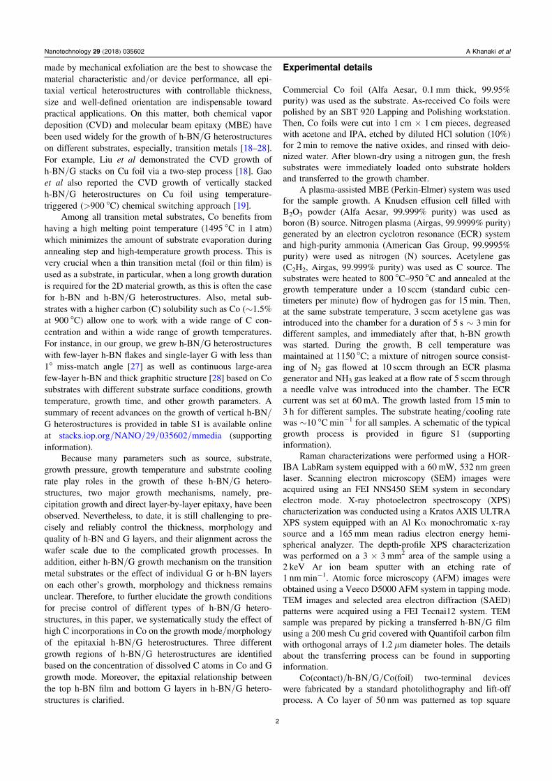
Figure 3 shows characterization results of h-BN/G sampleswith the same 30 s C treatment time and different h-BN growthtime. It can be seen in the SEM images of figures 3(a)–(d) thatthe coverage and size of the triangular h-BN flakes increases asthe increase of h-BN growth time and the whole Co substratesurface is almost covered with h-BN as the growth time reaches∼1 h. Figure 3(e) shows h-BN lateral growth speed as a functionof growth time. The area of h-BN coverage is obtained byImageJ software, as illustrated in figure S7 (supporting infor-mation) and the growth speed is defined as the area of coveragedivided by the growth time. As seen from figure 3(e), the h-BNlateral growth rate is relatively high in the short h-BN growthperiod (∼2.5%min−1 at 15min), and then gradually decreasesto lower values as the growth progresses (∼1%min−1 at 1 h).This further justifies the continuous morphology of the h-BNfilms for all samples grown for 3 h. It should be noted that theSEM image in figure 3(a) and OM image in figure 3(f) of the
4
Nanotechnology 29 (2018) 035602 A Khanaki et al

15min h-BN growth sample show the accumulation of C atoms(dark color) around triangular h-BN flakes. Figures 3(g) and (h)show graphene G peak Raman intensity mapping of figure 3(f)and corresponding Raman spectra from the point of the strongestRaman signal in figure 3(g), respectively. The Raman scatteringresults clearly support the findings from the microscopy studiesin figures 3(a) and (f). This behavior, i.e., C preferential pre-cipitation along h-BN triangle edges and/or grain boundariesduring the cooling process, is also consistent with the formationmechanism for the G network underneath the h-BN film ofh-BN/G samples in region 1 (figures 1 and 2). The graphene2D/G intensity ratio of the as-grown sample was calculated∼0.35 (figure 3(h)) which is much lower than that of G refer-ence sample in region 1, namely ∼0.6 (figure S6(b)). This fur-ther shows the effect of top h-BN film on the thickness ofunderneath G layers in region 1 samples. A wide FWHM of
h-BN E2g peak (∼65 cm−1) in figure 3(h) is due to the existenceof intrinsic graphene D peak in the sample (figure S6(c)).
Figure S8 (supporting information) shows Raman spec-trum and C1s, B1s and N1s XPS signals of a representativeregion 2 sample with a 1.5 min C treatment time, and AFMand OM images of the same sample after the h-BN/Gstructure was transferred onto a SiO2/Si substrate and itscorresponding h-BN E2g phonon mode intensity mapping.Since the isothermal G growth in this region is limited only tothe formation of a few G flakes/islands, the final G morph-ology in h-BN/G sample is a mixture of isothermal G growthand precipitation during the cooling process, resulting in anon-uniform G film. According to figure S8(f) (supportinginformation), despite the non-uniform morphology of Ggrowth in this region, the h-BN has been formed continuouslyand fully covered the sample’s surface.
Figure 2. Characterizations of h-BN/G samples in region 1. SEM images of the h-BN/G samples with (a) 5 s, (b) 30 s, and (c) 45 s Ctreatment time showing the G network morphology. (d) AFM image of h-BN/G sample with 30 s C treatment time transferred onto SiO2/Sisubstrate. (e) and (f) Raman spectra of the points (1) and (2) of (d), respectively. XPS signals of (g) C1s, and (h) B1s and N1s for as-grownh-BN/G sample with 30 s C treatment time. (i) OM image of the G reference sample with 30 s C time.
5
Nanotechnology 29 (2018) 035602 A Khanaki et al
Figure 4 shows characterization results of typical h-BN/G samples in region 3. Figure 4(a) shows Raman spectra of anas-grown h-BN/G sample with 3 min C treatment time at 13locations across the 1 cm×1 cm h-BN/G sample (indicatedin a photo image in the inset of figure 4(a)). The existence ofboth multilayer G (MG or thin graphite) and h-BN Ramanpeaks is evident. The 2D/G ratio of MG in this sample wascalculated ∼0.18. Figure 4(b) is the zoom-in spectra offigure 4(a) between 1200 and 1500 cm−1, showing excellentuniformity of h-BN E2g phonon mode’s position(∼1366.5 cm−1), intensity and full width at half maximum(FWHM ∼40 cm−1) over these 13 points of measurement[41]. A portion of the sample was transferred onto SiO2/Sisubstrate for the AFM measurement. The AFM image revealsthat the h-BN/G film has a total thickness of ∼133 nm(figure 4(c)).
To reveal the individual thickness of h-BN and MGlayers, we performed XPS sputtering depth profile measure-ment. Figures 4(d) and (e) show the evolution of C1s, andB1s and N1s XPS signals as a function of sputtering depthwithin 4 nm of the top surface of h-BN/G sample. As seen infigure 4(d), C1s peak is strongest when the sample was notsputtered, which is due to the inclusion of signals fromabsorbed C species on the surface or adventitious C [42].After removing the top 0.17 nm material, the intensity of C1speak drops significantly compared with the signal beforesputtering and then remains about the same with furthersputtering while the width of the C1s peak increases asthe sputtering depth increases (down to ∼1–2 nm) due to Ar+
beam induced damage. On the other hand, B1s and N1s XPSsignals in figure 4(e) decrease proportionally and gradually byremoving the top layers and become negligible when thesputtering depth reaches ∼2 nm (i.e., h-BN thickness).Figure 4(f) shows the calculated relative atomic concentrationfor B, N, and C as a function of the sputtering depth. As thesputtering depth increases, both N and B concentrationsdecrease gradually and reach an insignificant percentage at a
sputtering depth of 1–2 nm, while the C concentration gra-dually levels up and then becomes steady as the etching depthextends from 2 to 4 nm. Considering the AFM (figure 4(c))and XPS depth-profile (figure 4(f)) measurement results, itcan be concluded that the h-BN/MG structure has a top h-BNlayer of 1–2 nm and a bottom MG layer of 131–132 nm. Sucha large thickness of MG is believed to be caused mainly byprecipitation of dissolved C atoms during cooling process.Much higher substrate cooling rates could significantly reducethe total G thickness, although thermal strained inducedwrinkles could compromise the quality of the precipitated Gand/or h-BN in those cases [43]. Alternatively, other trans-ition metals with much less C solubilities can be used tocontrol the number of G layers down to a few layers [44, 45].Owing to the fact that these C atoms precipitate underneaththe isothermally grown MG buffer, the morphological andstructural uniformity of h-BN/G samples is well preserved, asinferred from figures 1(c) and (g). Moreover, similar h-BNthickness in region 1 (∼2.1 nm) and region 3 (1–2 nm)samples indicates that the h-BN vertical growth is not affectedby the G growth mechanism, morphology or thickness(figures 2 and 4). The seemly self-limited growth of h-BN onG with different morphology under the present growth con-dition is intriguing and needs further investigation. Similarself-limited growth of h-BN on metal substrates was alsoreported [46–50].
Figure 4(g) shows XRD pattern of the h-BN/G sample.The evident peaks at 26.64° and 54.79°, and 27.1° and 54.94°are assigned to (002) and (004) crystal plane diffractions of MGand h-BN films according to JCPDS card numbers 41-1487 and34-0421, respectively [51, 52]. The small peak at 51.5° is from(002) crystal plane diffraction of hcp Co (JCPDS# 01-071-4239) [53, 54]. Such intense XRD peaks indicate the highquality of MG and h-BN films in the sample. It also suggeststhat h-BN and MG have grown along the same orientation. Tofurther elucidate the growth relation between h-BN and MG, wetransferred a piece of the same sample onto a Cu grid and
Figure 3. H-BN time-dependent growth of region 1 h-BN/G samples with 30 s C treatment time. (a)–(d) SEM images of h-BN/G sampleswith 15, 30, 45 min and 1 h h-BN growth duration. (e) h-BN lateral growth speed and triangle edge length for samples in (a)–(d). (f) OMimage and corresponding (g) graphene G peak Raman intensity mapping and (h) Raman spectrum of (g) at its strongest signal point. H-BNE2g Raman peak at ∼1367 cm−1 has a FWHM of ∼65 cm−1 and graphene 2D/G intensity ratio is ∼0.35.
6
Nanotechnology 29 (2018) 035602 A Khanaki et al

performed TEM measurement (figure S9). Figure S9(a) shows abright-field top-view image of the transferred film on the TEMgrid, and figure S9(b) shows the SAED pattern obtained fromthe area in figure S9(a). A single hexagonal pattern is observed;however, the dots are slightly elongated, suggesting overlappinghexagonal patterns of h-BN and MG films with a negligiblemisalignment between each other. Figure 4(h) shows anabsorption spectrum of the sample after a portion of the h-BN/MG film was transferred to a sapphire substrate. As can be seenin figure 4(h), the clear absorption edge at ∼202 nm originatesfrom the band gap of h-BN film [55]. A big portion of UV lightspectrum has been also absorbed by the thick MG film [56].Figure 4(i) shows cross-plane I–V characteristic of aCo(contact)/h-BN/G/Co (substrate) two-terminal device. The
bottom inset shows a schematic of the device, which was fab-ricated using a process described in the Experimental section.The top inset displays the log-scale current versus voltagebehavior of the device, showing 3 distinct regions: (I) currentlinearly increases as the increase of voltage, which representsdirect-tunneling related conduction (V<∼0.6) [57, 58], (II)current nonlinearly/exponentially increases with the voltageunder moderate biases (∼0.6<V<∼1.25) due to the Fowler–Nordheim tunneling mode [59, 60], and (III) current sharplyincreases due to the dielectric breakdown at a bias of 1.25 V[61]. The calculated breakdown electric field based on an h-BNthickness of 1–2 nm is 6.25–12.5MV cm−1, which is compar-able with the observed values from other epitaxial h-BN films[61–63].
Figure 4. Characterization of h-BN/MG samples in region 3. (a) 13-points Raman spectra of the as-grown h-BN/MG sample with 3 min Ctreatment time and inset shows the sample photograph. The 2D/G ratio of G in this sample is∼0.18. (b) Zoom-in Raman spectra of (a) showingthe h-BN E2g phonon mode at ∼1366.5 cm−1 with a uniform FWHM of ∼40 cm−1 across these 13 points of measurement. (c) AFM image ofthe same sample transferred onto SiO2/Si substrate with the total thickness of ∼133 nm. (d) C1s and (e) B1s and N1s as a function of sputteringdepth in the depth-profile XPS characterization and (f) relative atomic concentration of C, B, and N versus sputtering depth.(g) XRD spectrum of the same sample. Inset is the magnified spectrum with 2theta from 54.7° to 55°. (h) UV absorption spectrum of the h-BN/MG sample transferred onto a sapphire substrate. (i) I–V characteristic of Co(contact)/h-BN/MG/Co(foil) two-terminal device structure withthe contact size of 25 μm×25 μm. The inset displays the log-scale current versus voltage behavior of the device with 3 distinct regions.
7
Nanotechnology 29 (2018) 035602 A Khanaki et al

Conclusion
We performed a systematic study of the in situ growth ofh-BN/G films on a Co substrate by sequentially introducing aC source with a high C incorporation, and B and N sources inan MBE system. It is found that the continuous h-BN/Gheterostructures can be formed at a substrate temperature of850 °C–900 °C. By changing the C amount incorporation, theh-BN/G structure alters from region 1 where the G network isformed only by precipitation during cooling process under-neath the h-BN film; to region 2 where isothermal G growthoccurs to form G islands partially covering the substrate,followed by further precipitation G growth, leading to a non-uniform h-BN/G structure, and to region 3 where a uniformh-BN/G heterostructure with a thin continuous h-BN and athick continuous MG are formed from both isothermal Ggrowth and precipitation. It is found that the top h-BN filminfluences the morphology, thickness and quality of under-neath G layers in h-BN/G samples of region 1. In addition,the h-BN growth is self-limited to a 1–2 nm thick film in allthree regions, regardless of the underneath G thickness ormorphology.
Acknowledgments
This work was supported in part by FAME, one of six centersof STARnet, a Semiconductor Research Corporation programsupported by MACRO and DARPA.
ORCID iDs
Jianlin Liu https://orcid.org/0000-0001-6513-0867
References
[1] Nag A, Raidongia K, Hembram K P S S, Datta R,Waghmare U V and Rao C N R 2010 ACS Nano 4 1539
[2] Liu L, Feng Y P and Shen Z X 2002 Phys. Rev. B 68 104102[3] Watanabe K, Taniguchi T and Kanda H 2004 Nat. Mat. 3 404[4] Hattori Y, Taniguchi T, Watanabe K and Nagashio K 2015
ACS Nano 9 916[5] Kim S M et al 2015 Nat. Commun. 6 8662[6] Novoselov K S A, Mishchenko A, Carvalho A and
Castro Neto A H 2016 Science 353 9439[7] Xia W, Dai L, Yu P, Tong X, Song W, Zhang G and Wang Z
2017 Nanoscale 9 4324[8] Schulman D S, Arnold A J, Razavieh A, Nasr J and Das S 2017
IEEE Nanotechnol. Mag. 11 6[9] Yankowitz M, Xue J, Cormode D, Sanchez-yamagishi J D,
Watanabe K, Taniguchi T, Jarillo-Herrero P, Jacquod P andLeRoy B J 2012 Nat. Phys. 8 382
[10] Aggoune W, Cocchi C, Nabok D, Rezouali K,Belkhir M A and Draxl C 2017 J. Phys. Chem. Lett. 8 1464
[11] Dean C R et al 2013 Nature 497 598[12] Cheng R et al 2017 Appl. Phys. Lett. 110 173507[13] Dean C R et al 2010 Nat. Nanotechnol. 5 722
[14] Amet F, Williams J R, Garcia A G F, Yankowitz M,Watanabe K, Taniguchi T and Goldhaber-Gordon D 2012Phys. Rev. B 85 073405
[15] Britnell L et al 2012 Science 335 947[16] Novoselov K S, Jiang D, Schedin F, Booth T J,
Khotkevich V V, Morozov S V and Geim A K 2005 Proc.Natl Acad. Sci. USA 102 10451
[17] Pacile D, Meyer J C, Girit C O and Zettl A 2008 Appl. Phys.Lett. 92 133107
[18] Liu Z, Song L, Zhao S, Huang J, Ma L, Zhang J, Lou J andAjayan P M 2011 Nano Lett. 11 2032
[19] Gao T, Song X, Du H, Nie Y, Chen Y, Ji Q, Sun J, Yang Y,Zhang Y and Liu Z 2015 Nat. Commun. 6 6835
[20] Wu Q, Jang S K, Park S, Jung S J, Suh H, Lee Y H, Lee S andSong Y J 2015 Nanoscale 7 7574
[21] Summerfield A et al 2016 Sci. Rep. 6 22440[22] Wofford J M, Nakhaie S, Krause T, Liu X, Ramsteiner M,
Hanke M, Riechert H and Lopes J M 2017 Sci. Rep. 7 43644[23] Plaut A S et al 2017 Carbon 114 579[24] Driver M S, Beatty J D, Olanipekun O, Reid K, Rath A,
Voyles P M and Kelber J A 2016 Langmuir 32 2601[25] Zheng R, Khanaki A, Tian H, He Y, Cui Y, Xu Z and Liu J
2017 Appl. Phys. Lett. 111 011903[26] Xu Z, Zheng R, Khanaki A, Zuo Z and Liu J 2015 Appl. Phys.
Lett. 107 213103[27] Zuo Z, Xu Z, Zheng R, Khanaki A, Zheng J-G and Liu J 2015
Sci. Rep. 5 14760[28] Xu Z, Khanaki A, Tian H, Zheng R, Suja M, Zheng J-G and
Liu J 2016 Appl. Phys. Lett. 109 043110[29] Ishida K and Nishizawa T 1991 J. Phase Equilib. 12 417[30] Zheng M et al 2010 Appl. Phys. Lett. 96 063110[31] Kassab L R P, Martinelli J R, dos Santos A D,
Ribeiro S J L and dos Santos M V 2016 Mater. Res. 19 669[32] McCarty K F, Feibelman P J, Loginova E and Bartelt N C 2009
Carbon 47 1806[33] Baraton L, He Z B, Lee C S, Cojocaru C S, Châtelet M,
Maurice J-L, Lee Y H and Pribat D 2011 Europhys. Lett. 9646003
[34] Hamilton J C and Blakely J M 1980 Surf. Sci. 91 199[35] Hu X, Bjorkman T, Lipsanen H, Sun L and
Krasheninnikov A V 2015 J. Phys. Chem. Lett. 6 3263[36] Luo J, Tian P, Pan C-T, Robertson A W, Warner J H,
Hill E W and Briggs G A D 2011 ACS Nano 5 1047[37] Ci L et al 2010 Nat. Mat. 9 430[38] Zheng R, Xu Z, Khanaki A, Tian H, Zuo Z, Zheng J-G and
Liu J 2017 Thin Solid Films 627 39[39] Xu Z, Tian H, Khanaki A, Zheng R, Suja M and Liu J 2017
Sci. Rep. 7 43100[40] Tonkikh A A, Voloshina E N, Werner P, Blumtritt H,
Senkovskiy B, Güntherodt G, Parkin S S P and Dedkov Y S2016 Sci. Rep. 6 23547
[41] Gorbachev R V et al 2011 Small 7 465[42] Barr T L and Seal S 1995 J. Vac. Sci. Technol. A 13.3 1239[43] Choi D S, Kim K S, Kim H, Kim Y, Kim T Y, Rhy S-H,
Yang C-M, Yoon D H and Yang W S 2014 ACS Appl.Mater. Interfaces 6 19574
[44] Zhao P, Kumamoto A, Kim S, Chen X, Hou B, Chiashi S,Einarsson E, Ikuhara Y and Maruyama S 2013 J. Phys.Chem. C 117 10755
[45] Takesaki Y, Kawahara K, Hibino H, Okada S, Tsuji M andAgo H 2016 Chem. Mat. 28 4583
[46] Orofeo C M, Suzuki S, Kageshima H and Hibino H 2013 NanoRes. 6 335
[47] Shi Y et al 2010 Nano Lett. 10 4134[48] Jang S K, Youn J, Song Y J and Lee S 2016 Sci. Rep. 6 30449[49] Preobrajenski A B, Vinogradov A S and Mårtensson N 2005
Surf. Sci. 582 21[50] Morscher M, Corso M, Greber T and Osterwalder J 2006 Surf.
Sci. 600 3280
8
Nanotechnology 29 (2018) 035602 A Khanaki et al

[51] Stobinski L, Lesiak B, Malolepszy A, Mazurkiewicz M,Mierzwa B, Zemek J, Jiricek P and Bieloshapka I 2014J. Electron Spectrosc. Relat. Phenom. 195 145
[52] Bhimanapati G R, Kozuch D and Robinson J A 2014Nanoscale 6 11671
[53] Chioncel F M and Haycock W P 2005 Chem. Vap. Depos.11 235
[54] Khanaki A, Xu Z, Tian H, Zheng R, Zuo Z, Zheng J-G andLiu J 2017 Sci. Rep. 7 4087
[55] Zhang C, Zhao S, Jin C, Koh A L, Zhou Y, Xu W, Li Q,Xiong Q, Peng H and Liu Z 2015 Nat. Commun. 66519
[56] Meng J H, Zhang X W, Wang H L, Ren X B, Jin C H,Yin Z G, Liu X and Liu H 2015 Nanoscale 7 16046
[57] Simmons J G 1963 J. Appl. Phys. 34 2581[58] Lee G H, Yu Y J, Lee C, Dean C, Shepard K L, Kim P and
Hone J 2011 Appl. Phys. Lett. 99 243114[59] Pandey S et al 2014 Nanoscale 6 3410[60] Ji Y et al 2016 Appl. Phys. Lett. 108 012905[61] Britnell L et al 2012 Nano Lett. 12 1707[62] Hui F, Pan C, Shi Y, Ji Y, Grustan-Gutierrez E and Lanza M
2016 Microelectron. Eng. 163 119[63] Hattori Y, Taniguchi T, Watanabe K and Nagashio K 2016
Appl. Phys. Lett. 109 253111
9
Nanotechnology 29 (2018) 035602 A Khanaki et al