effect of texture and zn content on etch morphology of the...
TRANSCRIPT

TMT4500 PROJECT IN MATERIALS TECHNOLOGY
AUTUMN 2008
Effect of texture and Zn content on etch morphology of
the aluminium alloy EN-AW 6063
Astrid Bakken
Supervisor: Professor Kemal Nisancioglu (NTNU)
Co-supervisors: Otto Lunder (SINTEF), Dr, Øystein Bauger (Hydro Sunndal)
DEPARTMENT OF MATERIALS SCIENCE AND ENGINEERING
2
Preface
This project in cooperation with Hydro, SINTEF and NTNU has been carried out at the
Department of Materials and Engineering, Norwegian University of Technology and
Engineering (NTNU) and SINTEF Oslo in the period from August to December 2008.
The supervisors of this project have been Professor Kemal Nisancioglu1, Dr. Øystein Bauger2
and Otto Lunder3. I am grateful for their interest in this project, and I would like to thank
them for their guidance and help.
I would like to give a special thank to Børge Holme3 for the help with White Light
Interforometry and Secondary Ion Mass Spectrometry measurements, but at the most I would
like to thank him for inspiration and long discussions.
Engineer Kjell Røkke1 deserves thanks for helping me getting started in the laboratory.
Morten Karlsen1 for helping me with access to the SEM-lab.
Astrid Bakken
19.12.2008 Trondheim
1:NTNU, 2:Hydro Sunndal, 3:SINTEF

3
Summary
In the industry a surface defect is observed on extruded aluminium alloys called grainy
appearance. Earlier investigations have shown that Zn plays a major role contributing to this
defect, which is a result of preferential etching of grains. So far the mechanism for this
surface defect is still not known. In this project the effect of Zn in the aluminium alloy EN-
AW 6063-T6 is investigated.
Correct processing parameters (time, temperature, extrusion speed etc.) in the fabrication of
extruded aluminium profiles are important for the surface appearance. The surface defect is a
result from etching in alkaline solution, where the surface is treated to obtain uniform even
finish and to avoid filiform corrosion. Alluminium alloys have in general very good corrosion
resistances due to formation of aluminium oxide.
The influence of texture and Zn on etch morphology (etching in NaOH) is studied with
Electron BackScatter Diffraction (EBSD), White Light Interferometry (WLI) and Secondary
Ion Mass Spectrometry (SIMS). These techniques give information of crystallographic
orientation, topography and chemical composition on the surface respectively.
From crystallographic orientation and topography measurements it is observed higher
dissolution rate of grains with {111} orientation compared to {100} and {110} oriented
grains. Enrichment of Zn and Cu is found on {111} oriented grains when chemical
composition is compared with topography and crystallographic orientations. The preferential
etching could be due to potential distinction between grains with different orientation.
Selective dissolution of aluminium could be the cause of enrichment.

4
Table of Contents
1 Introduction ........................................................................................................................ 6
1.1 Aim of project ............................................................................................................ 7
2 Background ........................................................................................................................ 8
2.1 Production of extruded aluminium profiles ............................................................... 8
2.1.1 Extrusion of aluminium profiles ........................................................................ 9
2.1.2 Anodising; Surface treatment and finishing ....................................................... 9
2.2 Aluminium alloy EN-AW 6063 ............................................................................... 11
2.3 Corrosion of Aluminium .......................................................................................... 12
2.3.1 Galvanic corrosion ........................................................................................... 12
2.3.2 Filiform corrosion ............................................................................................ 13
2.3.3 Pitting corrosion ............................................................................................... 13
2.4 Electron BackScatter Diffraction (EBSD) ............................................................... 13
2.5 White Light Interferometry (WLI) ........................................................................... 14
2.6 Secondary Ion Mass Spectrometry (SIMS) .............................................................. 15
2.7 Previous work ........................................................................................................... 16
2.7.1 Effect of Zn in the etching bath ........................................................................ 16
2.7.2 Effect of Zn in the alloy ................................................................................... 17
2.7.3 Preferential etching .......................................................................................... 18
3 Experimental procedure ................................................................................................... 19
3.1 Peripheral preprocessing .......................................................................................... 19
3.2 Etching trials ............................................................................................................ 19
3.3 Electron BackScatter Diffraction (EBSD) ............................................................... 19
3.4 White Light Interferometry (WLI) ........................................................................... 20
3.5 Secondary Ion Mass Spectrometry (SIMS) .............................................................. 20
4 Results .............................................................................................................................. 21
4.1 Grain height distribution and SEM .......................................................................... 21
4.2 Topography and grain orientation ............................................................................ 22

5
4.3 Depth profiles from Secondary Ion Mass Spectrometry (SIMS) ............................. 24
4.4 Elemental mapping from Secondary Ion Mass Spectrometry (SIMS) ..................... 27
5 Discussion ........................................................................................................................ 30
5.1 Discussion of the measuring techniques .................................................................. 30
5.2 Preferential etching of crystallographic orientation ................................................. 31
5.3 Deposition of Zn and Cu .......................................................................................... 31
6 Conclusion and outlook .................................................................................................... 33
7 References ........................................................................................................................ 34
Appendix
A Calculations of sputter depth and relative intensities .......................................................... І
B Intensities of Zn and Cu as a function of sputter depth ..................................................... П
C Crystallographic map ....................................................................................................... Ш

6
1 Introduction
Aluminium is today the worlds second most commonly used metal.[1] In nature aluminium is
occurring as bauxite. The first commercial process for producing aluminium began with
Henry Deville in 1854[2], since then there has been a huge revolution in processing of
aluminium and its alloys. Even though the technology is much better today there are still
many challenges in the industry; Emission control, waste disposal and energy efficiency are a
few. Aluminium recycling began in the early 1900s and the production has today a capital
cost 80-85% less than the primary production from bauxite. Recycling of aluminium result in
a higher amount of trace elements, and one problem is surface defects after extrusion and
anodising.
Spangling effect is an often observed surface defect after the anodising step in the production
line. It is proposed divided into three categories; grainy, galvanizing and -sparkling
appearance. Grainy appearance is described as grains visible with the eye on the surface after
alkaline etching. Whereas galvanizing effect is a surface with a few shiny grains and sparkling
appearance is a general shiny surface[3]. Investigations have shown the phenomenon of grainy
appearance is dependent on the chemical composition of the material. During alkaline etching
it is observed enrichment of zinc and cupper for Al-Zn and Al-Cu alloy respectively[4].
Copper and zinc together with a certain grain size, texture and free Zn in the etching bath is
believed to increase the susceptibility of grainy appearance[5].
This investigation is based on previous master thesis performed by Nina Ljones[3], Siv Malm
Nortømme[6] and David Franke[7] in cooperation with Hydro. In general it was observed Zn
promotes preferential etching of grains. Nina Ljones found by adding Zn to the etching bath
resulted in increase of grainy appearance. Siv Malm Nortømme investigated alloys with
different amount of Zn and observed higher amount of Zn resulted in higher susceptibility of
grainy appearance. The preferential etching of the surface was investigated by White Light
Interferometry (WLI) and Electron BackScatter Diffraction (EBSD). Nina Ljones found that
{111} oriented grains were etched more compared to other grain orientations, however Siv
Malm Nordtømme could not verify this due to lack of {111} oriented grains.
7
1.1 Aim of project
It is known from industry (and N. Ljones master thesis) that Zn in the etching bath can have
detrimental effect on the surface appearance. In this project it is desirable to investigate the
effect of Zn in the material. The texture and enrichment of Zn on the surface after etching in
alkaline solution will be studied on the aluminium alloy EN-AW 6063-T6. Based on earlier
investigations, measurements will be performed trying to verify the preferential etching of
{111} orientated grains. This will be investigated by using Electron BackScatter Diffraction
(EBSD) and White Light Interferometry (WLI) to measure grain orientations and topography
respectively. In addition chemical composition of the surface after etching will be emphasised
by using Secondary Ion Mass Spectrometry (SIMS) which is a very surface sensitive
technique. Understanding the mechanism of how Zn effect the etching morphology is a
superior goal.

8
2 Background
2.1 Production of extruded aluminium profiles
Every step in the production of a finished product influences the final surface appearance. It is
therefore important to control the time and temperature profiles in every step in the
production line; the temperature sequence for the production line for EN-AW 6063 is shown
in Figure 2.1. There are two main routes for producing aluminium; primary from mainly
bauxite and secondary from recycled aluminium. Secondary melted aluminium is often added
to the primary melt and requires far less energy to produce aluminium than primary
aluminium. Here only the primary production path will be considered for extruded profiles
due to the EN-AW 6063 extruded profile.
Figure 2.1: Temperature sequence during the production line of aluminium[8]
9
2.1.1 Extrusion of aluminium profiles
Bauxite is the starting point and through the Bayer process alumina is produced. Alumina is
reduced electrochemical according the Hall-Héroult process to molten aluminium. Then the
aluminium is either cast as ingots or extrusion billets at a temperature of approximately
700ºC. Ingots are remelted and used for casting whereas the extrusion billets are used for
further extrusion processing.
After casting the profiles are homogenised at 580 ºC for a few hours. This step is necessary at
first to remove solute concentration gradients which are appearing after the supercooling from
the casting step. Secondary to reintroduce the crystals and intermetallics formed or
precipitated at the grain boundaries into the solid solution.[2]
In the extrusion process the billets are reheated to 460-500 ºC and are forced by hydraulic
pressure through an orifice in a die. Extruded profiles are usually rods, foils, bars or hollow
sections. The first part of the extruded profile, few mm, has the same structure as the casted
material, but during the extrusion the grains are distorted and the constituents aligned in the
extrusion direction. Grains are affected by temperature and strain and are therefore hot
worked and recrystallized. The temperature should be high enough to allow for micro-
recrystallisazation but low enough to avoid eutectic melting. To obtain a good surface finish a
high extrusion speed is favourable, but is often limited due to formation of transverse cracks
from the die. [2]
After extrusion the profiles are artificially aged by heating up to 185 ºC for 5 hours. This
process strengthens and hardens the material, where the EN-AW 6063 alloy precipitates from
a supersaturated solid solution to Mg2Si having a face centred cubic structure.[10]
2.1.2 Anodising; Surface treatment and finishing
For different applications of aluminium the right surface treatment is applied to give the
wanted surface appearance and serviceability to the final product.

10
Prior to etching the extruded aluminium profiles are degreased, where oil, grease and other
unwanted impurities are removed. This is executed to obtain high degree of uniformity prior
to etching. Etching is performed in caustic soda, and additives may be added to the bath
depending on the wanted effect (matt, rough surface etc.). The purpose of etching is to
remove the natural formed oxide which can contain defects. Aluminium is dissolved
according to reactions given in equation 1, exothermic rx, with the formation of hydrogen and
alumina.
2 2 2
2 4 2
2 2 2 2 3
2 2 6 2( ( ) ) 3
Al NaOH H O NaAlO H
Al OH H O Al OH H− −
+ + → +
+ + → + (1)
In long time etchants there will be a build up of impurities in the bath. Only a few p.p.m. of
zinc in the solution will give rise to the surface defect galvanizing appearance, see Figure 2.2.
This is a preferential grain etching effect, which is prevented by addition of sulphides or
chromates.[11]
Figure 2.2: Galvanizing appearance on etched 6063 extrusion[11]
.
During the etching procedure a smut layer (gray-black film) is formed on the surface. It
contains elements as silicon, iron, cupper and other alloying elements. This is removed in a
nitric acid solution[12].

11
In the anodising step the oxide layer on the surface is thickened, up to 20 µm, by an
electrolytic process to improve the corrosion resistance and obtain nice visual surface.
Aluminium is used as the anode and lead is usually used as cathode. When current is flowing
oxygen reacts with aluminium to produce porous aluminium oxide. The pores have to be
sealed to obtain a high quality of the surface; this is performed in hot water (98ºC).
2.2 Aluminium alloy EN-AW 6063
The aluminium alloy EN-AW 6063 is one of the most frequently used extruded aluminium
alloy. It is used in automotive industry, medium strength purposes in building industry,
architectural purposes with good surface finishing and heat transfer applications. The larger
variety of applications is due to the good corrosion resistance, surface finish and a superior
response to the anodizing step. A low content of magnesium in the alloy gives a good
formability but with the expense of mechanical properties, whereas high level of magnesium
gives good mechanical properties. Corrosion of aluminium alloy is affected by the alloying
elements. Copper is the element with the most negative effect on corrosion resistance,
whereas Mn has the lowest effect. Silicon can play a slight role, and together with iron this
effect is coming more pronounced[11].The chemical composition of the alloy is given in Table
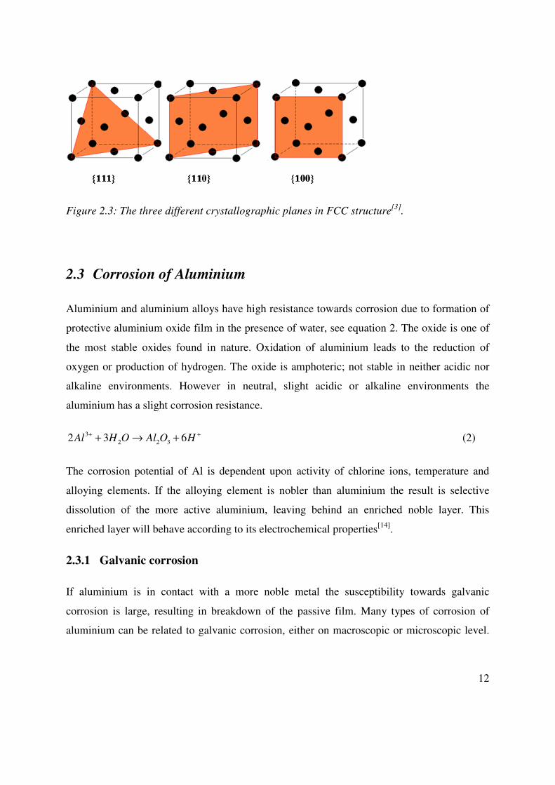
2.1. [13] Aluminium has a face centred cubic crystal (FCC) structure,
Figure 2.3.
Table 2.1: Chemical composition in wt% of EN-AW 6063[13]
.
Si Fe Cu Mn Mg Cr Zn Ti
EN-AW 6063 0.2-0.6 0-0.35 0-0.1 0-0.1 0.45-0.90 0-0.1 0-0.1 0-0.10
12
Figure 2.3: The three different crystallographic planes in FCC structure[3]
.
2.3 Corrosion of Aluminium
Aluminium and aluminium alloys have high resistance towards corrosion due to formation of
protective aluminium oxide film in the presence of water, see equation 2. The oxide is one of
the most stable oxides found in nature. Oxidation of aluminium leads to the reduction of
oxygen or production of hydrogen. The oxide is amphoteric; not stable in neither acidic nor
alkaline environments. However in neutral, slight acidic or alkaline environments the
aluminium has a slight corrosion resistance.
3
2 2 32 3 6Al H O Al O H+ +
+ → + (2)
The corrosion potential of Al is dependent upon activity of chlorine ions, temperature and
alloying elements. If the alloying element is nobler than aluminium the result is selective
dissolution of the more active aluminium, leaving behind an enriched noble layer. This
enriched layer will behave according to its electrochemical properties[14].
2.3.1 Galvanic corrosion
If aluminium is in contact with a more noble metal the susceptibility towards galvanic
corrosion is large, resulting in breakdown of the passive film. Many types of corrosion of
aluminium can be related to galvanic corrosion, either on macroscopic or microscopic level.

13
Electrical resistance of metal path, conductivity of the electrolyte, cathode/anode ratio and
polarisation of the cathode are factors affecting galvanic corrosion[14].
2.3.2 Filiform corrosion
Attack of the surface beneath coatings is called filiform corrosion[11]. The surface suffers only
a small damage, but the surface appearance is detrimental altered. The susceptibility of
filiform corrosion is increased with surface shear during rolling, grinding or machining
developing an ultra-fine grained surface structure[15]. Filiform corrosion can be avoided by
etching and anodizing, removing this surface layer[16].
2.3.3 Pitting corrosion
Pitting corrosion in salt water occurs at weak spots in the oxide film around intermetallic
particles and at grain boundaries[17]. It is dependent on the properties, size and distribution of
these intermetallics in the aluminium matrix. They are electrochemical nobler than the Al
matrix and act as the cathode. The pH decreases in the pit whereas it increases around the
cathodic site leading to etching of Al adjacent to the cathodic site. With the selective
dissolution of Al, due to microgalvanic effect, the nobler intermetallics are enriched at the
surface. The pits surface will however repassivate due to the detachment of intermetallic
particles[16],[18].
2.4 Electron BackScatter Diffraction (EBSD)
Electron BackScatter Diffraction (EBSD) together with Scanning Electron Microscope (SEM)
is used to identify crystallographic orientation in the material. The technique can also be used
to identify different phases, dislocations and grain boundaries. It uses a phosphor screen
detector which is placed at an angle with respect to the sample, Figure 2.4. The tilt angle is
70o, giving a good spatial resolution.

14
Figure 2.4: Electron BackScatter Diffraction principe[19, 20]
.
The incident beam must hit the surface at small angel (~20o) for the possibility of collecting
the emitted electrons by the detector and the signal is converted to visual picture with CCD
camera. The diffracted electrons are detected as Kikuchi patterns where each line in the
pattern is formed according to Bragg’s law of diffraction. The specific orientation of these
lines corresponds to the crystal structure of the sample and can be mathematically competed
to a crystallographic map by scanning the area of interest. Each point on the area of interest
corresponds to crystal structure with a specific orientation.[20]
2.5 White Light Interferometry (WLI)
With the use of White Light Interferometry (WLI) microscope the topography of the surface
is determined. A schematically illustration of WLI instrument is shown in Figure 2.5. The
technique uses a coherent light source (S1) and the beamsplitter (B1) divides the beam. One
beam hits the reference mirror (M1) and is reflected whereas the other is reflected by the
object of investigation (O). The beams are recombined at the imaging lens (L3) and the
difference in optical path way is recorded by a CCD camera.[20, 21]

15
Figure 2.5: Schematic illustration of WLI[21]
.
2.6 Secondary Ion Mass Spectrometry (SIMS)
Secondary ion mass spectrometry (SIMS) is a surface analytical technique that can detect low
concentrations of impurities and alloying elements. The instrument is build up of a primary
ion column, secondary ion extraction system, mass spectrometer and detection system, Figure
2.6. The technique uses a primary ion gun, which can be focused to less than 1 µm in
diameter, to bombard the surface in ultra high vacuum. The ion gun can either be oxygen or
caesium source. Secondary ions together with atoms and molecules are emitted having
variations in energy. Di and triatomic secondary ions have a lower kinetic energy than
monovalent atoms. The secondary ions are extracted and analysed in the mass spectrometer.
They are separated according to the mass/charge ratio in the magnetic field and are further
detected and analysed by phosphorous screen or CCD camera. This gives detailed information
on the chemical composition on the surface. Depending on the wanted analysis two different
techniques can be used; static or dynamic SIMS. In static SIMS slow sputter rate is used
resulting in the removal of only a tenth of an atomic layer. This is used when molecular
species is identified. In the dynamic SIMS higher sputter rate is used with the result of a more
damaged surface. With this technique quantitative information is obtained, and is the case
when depth profiling is performed. The depth profiles are the result of counting the secondary
ions of interest as function of sputter time. Instead of depth profiles ion images can be

16
recorded, showing the intensity of secondary ions on the sample surface. The detection limit
of the instrument is between 1012 and 1016 atoms/cm2 and is dependent on the performance of
the vacuum system. [22]
Figure 2.6: Schematic illustration of Secondary Ion Mass Spectrometry [23]
.
2.7 Previous work
This investigation is based on previous master thesis by Nina Ljones (2006)[3], David Franke
(2008)[7] and Siv Malm Nordtømm (2008)[6]. Here are the important results given.
2.7.1 Effect of Zn in the etching bath
From the industry it was belived that Zn had a tremendous effect on the surface defect grainy
appearance. The influence of dissolved Zn in the etching bath was therefore investigated by
weight loss measurements. Nina Ljones observed that a high amount of dissolved Zn in the
etching bath resulted in decrease in weight losses of the samples together with a more
preferential etched surface. This indicating some layer of Zn was blocking the further etching
of the surface. This was also indicated by the decrease in corrosion potential when etching in
solution containing dissolved Zn. The decrease in the potential was found to be 50 mV. From
Glow Discharge Optical Spectrometry (GD-OES) analysis, showing weight percent of Al, Si,

17
Mg, Zn and O as function of sputter depth, it was observed that etched samples in the solution
with dissolved Zn had higher amount of Zn on the surface compared with etching in a
solution not containing dissolved Zn.
Nina Ljones also observed a more grainy surface appearance was dependent on amount of Zn
in the etching bath. Higher amount of Zn lead to higher degree of grainy appearance.
Additives from the anodising plant at Hydro Karmøy (HAP-K) added to the etching bath with
dissolved Zn resulted in no grainy appearance defect. This indicates that Zn reacts with the
additives
2.7.2 Effect of Zn in the alloy
Siv Malm Nortømme investigated the effect of Zn content (0.028, 0.11, 0.22 wt%) in a
aluminium alloy. Na2S (0.0025 g/L) was added to the etching bath to investigate if Zn was
deposited from the solution or selectively dissolved from the alloy, however no effect was
observed. Siv Malm Nordtømme discussed this was due to low concentration of Na2S. The
effect should be visible by precipitation of white ZnS if Zn was present in the solution. Higher
degree of grainy appearance was observed for longer etching time for both alloys containing
0.11 and 0.22 wt% Zn. Indicating that Zn favours grainy appearance. From weight loss
experiments Siv Malm Nortømme observed the alloy with lowest amount of Zn in the alloy
showed the highest weight loss compared to higher amount of Zn showing less weight loss.
The high weight losses she discussed from chance in corrosion mechanism going from pitting
attack to galvanic corrosion resulting in preferential etching of grains.
David Franke investigated two samples; one with low amount of Zn and Cu (0.00052,
0.00103 wt%) and the other high amount of Zn and Cu (0.04448, 0.03224wt%). They were
etched and aged (oil bath at 185ºC). He found the alloy containing high amount of Zn was
attacked more locally, grain boundaries and certain grains, compared with the alloy with low
amount of Zn giving more uniformly attack on the surface. There was also a correlation
between the ageing of materials and etching response. Longer aging time up to a certain time
resulted in higher etching response on the grain boundaries. He also performed weight loss
measurements and found the alloy containing low amount of Zn had higher weight loss.
18
2.7.3 Preferential etching
The effect of texture on etching response was analyzed by topography measurements and
crystallographic mapping by WLI and EBSD respectively. Nina Ljones observed {111}
oriented grains were etched more than {100} orientated grains. She proposed a mechanism
concerning this result from the packing density of the different grains; {100} oriented grains
have lower packing factor and it is energetically favourable for precipitation of Zn on this
orientation. From this she discussed that due to the microgalvanic effect between Al and Zn it
was expected preferential etching of {111} oriented grains. However the preferential
precipitation was not verified.
No correlation between preferential etched grains and orientation was found by Siv Malm
Nortømme because lack of {111} oriented grains on the surface.

19
3 Experimental procedure
The sample in investigation is an experimental alloy based on EN-AW 6063-T6, with a high
content of Zn (0.8 wt%). It was provided by Otto Lunder (SINTEF) and was produced at
Hydro Sunndal. The performed experimental sequence was polishing, WLI, etching, WLI,
SIMS, WLI, electropolishing and EBSD mapping. This showed to give good results. The
experiment was only performed on one sample because of only one sample holder in the
SIMS, however several sample points were investigated. WLI, SIMS and EBSD were
performed at the same location on the sample.
3.1 Peripheral preprocessing
The received samples were cut in small pieces (2x2 cm2) for use in the investigation.
All the samples were first grinded with grit paper from 800 to 4000 and then polished by
using diamond paste 3 µm and 1 µm.
On the final polished sample a scratch was made on the surface, making sure the same area
was investigated for later comparison.
3.2 Etching trials
The etching was performed by dipping the sample in 10 wt% NaOH solution (100 mL). The
temperature of the etching bath was constant at 60 ±1 oC and the etching time was 30 seconds.
3.3 Electron BackScatter Diffraction (EBSD)
The EBSD surface analysis was performed with Hitachi S-4300SE. The parameters used in
the investigation are presented in Table 3.1.
Electropolishing was performed to obtain good picture in EBSD.

20
Table 3.1: Operating parameters in EBSD
Tilt [º] 70
Working distance [mm] 20
Acceleration voltage [kV] 20
Step size [µm] 5
3.4 White Light Interferometry (WLI)
Topography of the sample was measured after etching and after investigation with SIMS.
Height of grains after etching and the sputter depth from SIMS was measured with the
software Vision 32. The topography analysis was performed at SINTEF Oslo with WYKO
NT-2000 from Veeco Instruments.
3.5 Secondary Ion Mass Spectrometry (SIMS)
Elemental mapping of Cu and Zn and depth profiles on certain grains were obtained by using
an oxygen ion source by the dynamic SIMS model CAMECA ims7f, University of Oslo. To
find the right isotopes of the elements important for this investigation a mass spectre was
performed. It was found the isotopes 1H, 63Cu, 66Zn and 27Al3 did not overlap with any
other possible peaks, so these were used further in the investigation. The depth profiles were
performed by finding the wanted grains by the light microscope incorporated in the SIMS and
using a raster size of 80х80 nm. Normal sputter time was 250 seconds. The raw data obtained
gives the relation between intensity [counts pr seconds] and sputter time. By calculations the
sputter time can be given by the sputtering depth. For calculations see appendix A. In the
elemental mapping of Cu and Zn the sample was sputtered until a depth of 140 nm was
obtained and then the pictures was taken based on the intensities of Cu, Zn and Al.

21
4 Results
4.1 Grain height distribution and SEM
Topography measurements were performed after grinding down to 4000, polishing down to 1
µm and after etching. The height distribution is shown in a histogram, see Figure 4.1. What
can be observed is that after polishing down to 1 µm the grains are normal distributed within a
region of ±112 nm. This is much better than only grinding to 4000 or polishing down to 3 µm.
After etching the grain height is no longer normal distributed because of the lack of
symmetry, and the height varies between ± 1000 nm. Figure 4.2 shows a picture taken in SEM
after etching. It can be observed preferential etching of some grains, small pits and particles
on the surface.
Figure 4.1: Histogram showing height distribution of grains from WLI measurement. Black
curve: grinding to 4000, red curve: polishing to 3 um, blue curve: polishing down to 1 um,
green curve: after etching in 10wt% NaOH.

22
Figure 4.2: SEM picture after etching in 10 wt% NaOH at 60ºC for 30 s.
4.2 Topography and grain orientation
The topography picture shown in
Figure 4.3 gives the relative height of grains after etching. Dark blue grains are low grains
whereas red grains are high grains. Low grains are etched more than higher grains. In
Figure 4.4 is the crystallographic orientation taken from the same area as the topography map.
The inverse pole figure indicates grains with {111} orientation are blue, {100} oriented grains
are red and {101} oriented grains are green. By comparing these two figures (notice that these
pictures are tilted compared to each other, and some grains in the EBSD map is etched to the
same height) the low grains from the topography map is recognized as {111} oriented grains.
The indexing of the same grains gives this relation.

23
Figure 4.3: Topography map showing grain height after etching (WLI)
Figure 4.4: EBSD-SEM picture showing crystallographic orientation of grains.

24
4.3 Depth profiles from Secondary Ion Mass Spectrometry (SIMS)
Figure 4.5 shows the same topography area as Figure 4.3. The difference is the dark blue
squares located within specific grains, indicating the location of the depth profiles. The crater
K (Figure 4.5) was sputtered at longer time (818 seconds) compared to the normal sputtering
time (250 seconds). This was performed as to find the relation between sputter times and
sputter depths (Appendix A). From each depth profile the intensity of the elements is found as
a function of sputter time (sputter depth), this is shown in Figure 4.6 for crater (a). The
intensities are all relative to the bulk aluminium signal (calculations in Appendix A). The
intensity of H, Zn and Cu decreases with sputter depth, whereas the intensity of Al is
increasing with sputter depth.
Figure 4.5: Topography map with depth profiles (WLI)

25
SIMS depth profiles
0,01
0,10
1,00
10,00
100,00
0 50 100 150 200 250 300 350 400 450 500
Sputter depth [nm]
Inte
ns
ity
re
lati
ve
to
Al
bu
lk s
ign
al
H
Cu
Zn
Al
Figure 4.6: Typical SIMS depth profile graph showing the relative intensities of the elements
H, Cu, Zn and Al as function of sputter depth.
In Figure 4.7 and Figure 4.8 the intensities of Zn and Cu are plotted as a function of the
sputter depth. The different graphs are related to one certain depth profile within a grain. Only
a selection of the comparison of heights is shown (all depth profiles are given in Appendix B).
The grain height of the grains was measured from the topography map taken before the SIMS
depth profiles were performed. Low grains show a higher intensity of both Zn and Cu than
higher grains. This trend is observed at a sputter depth from approximately 100 nm to 175 nm.
The relation between the intensity of Zn and Cu is plotted as function of grain height. This
relation is shown in Figure 4.9 for Zn and Figure 4.10 for Cu at certain sputter depths (94, 122
and 152 nm). The correlation between Zn and Cu on the surface as function of the grain
height is rather poor. However it can be observed better correlation at sputter depth of 152 nm
than at 93 nm, this is given by the linear deviation value R. Ideally this should be close to one,
indicating good correlation.

26
0 50 100 150 200 250 300 350 400
0,1
1 high
high
low
low
Inte
ns
ity o
f Z
n r
ela
tive
to
Al
bu
lk
Sputter depth [[[[nm]]]]
Grain heights:
Figure 4.7: Comparison of the relative intensities of Zn with sputter depth (sputter time) from
depth profiles.
0 50 100 150 200 250 300 350 400
0,1
1
high
high
low
low
Inte
nsit
y o
f C
u r
ela
tiv
e t
o A
l b
ulk
Sputter depth [[[[nm]]]]
Height of grains:
Figure 4.8: Comparison of the relative intensities of Cu with sputter depth (sputter time) from
depth profiles.

27
R2 = 0,35
R2 = 0,26
R2 = 0,15
0
0,5
1
1,5
2
2,5
-600 -400 -200 0 200 400
Grain hight [nm]
Inte
ns
ity
of
Zn
re
lati
ve
to
Al
bu
lk s
ign
al
94 nm
122 nm
152 nm
Figure 4.9: Correlation between Zn on the surface and height of grains after etching.
R2 = 0,43
R2 = 0,37
R2 = 0,20
0
0,1
0,2
0,3
0,4
0,5
0,6
0,7
0,8
-600 -400 -200 0 200 400
Grain hight [nm]
inte
ns
ity
of
Cu
re
lati
ve
to
Al
bu
lk s
ign
al
94 nm
122 nm
152 nm
Figure 4.10: Correlation between Cu on the surface and height of grains after etching
4.4 Elemental mapping from Secondary Ion Mass Spectrometry
(SIMS)

28
From the elemental mapping in SIMS the images b), c) and d) in Figure 4.11 were obtained.
Image a) is the topography map of the same area and the grains are indexed for easier
comparison. High intensities of Al, Zn and Cu is represented with brighter colour, and is an
indication of amount of the respective elements found on the surface. The grains G7 and G2
are low grains and have {111} orientation. These grains are easy to recognize in image b),
with dark brightness indicating lower intensity of Al (EBSD map in Appendix C for the same
are of investigation). The same grains have a high brightness in the Zn and Cu image and it
can therefore be said these grains contains higher amount of Zn and Cu.
Figure 4.11: Elemental mapping from SIMS; a) Topography map b) Al map c) Zn map d) Cu map.
Brighter colour represents higher intensities of the respective elements.
29
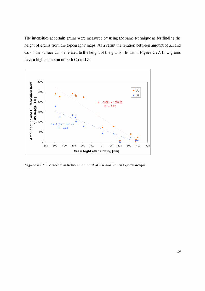
The intensities at certain grains were measured by using the same technique as for finding the
height of grains from the topography maps. As a result the relation between amount of Zn and
Cu on the surface can be related to the height of the grains, shown in Figure 4.12. Low grains
have a higher amount of both Cu and Zn.
y = -1,75x + 643,75
R2 = 0,92
y = -3,07x + 1200,69
R2 = 0,92
0
500
1000
1500
2000
2500
3000
-600 -500 -400 -300 -200 -100 0 100 200 300 400 500
Grain hight after etching [nm]
Am
ou
nt
of
Zn
an
d C
u m
ea
su
red
fro
m
SIM
S im
ag
e [
a.u
.]
Cu
Zn
Figure 4.12: Correlation between amount of Cu and Zn and grain height.

30
5 Discussion
5.1 Discussion of the measuring techniques
In the beginning of this project a different experimental sequence was used; First polishing,
electropolishing, EBSD, etching in NaOH, electropolishing, EBSD, WLI and SIMS. Based on
this sequence it was observed an even surface origin from the electropolishing step. Hence it
was difficult to indentify the grains found in the EBSD map with the topography map (WLI).
This also resulted in difficulties in the SIMS measurements due to the lack of finding specific
grains with wanted height. The experimental sequence was therefore changed (see chapter 3)
In Figure 4.6 the intensity of H, Zn and Cu decreases whereas the intensity of the Al signal is
increasing with sputter depth. The H signal is used as an indication of where the oxide layer is
ending and the beam starts to measure on the aluminium surface. In earlier investigations,
performed at SINTEF by Børge Holme, of sputter depths on aluminium the intersection of the
H signal and the Cu signal was used as the reference of the oxide/alloy interface. This gave
quite good relation between intensity of Zn and grain height, however it was observed better
correlation at longer sputtering times. Based on this it was decided to use the intersection of
the H and Zn signal which is lower in depth (longer sputter time) than the intersection
between H and Cu signal. The thickness of the oxide layer together with the smut layer
(resulting from etching) is approximately 140 nm. Since the amount of Zn is 0,8 wt%
compared to the low content of Cu it is not surprising that the intensity of Zn is higher than
the intensity of Cu.
The different result obtained from the depth profiles and elemental mapping can be accounted
for by comparing the two measuring techniques. Figure 4.9, Figure 4.10 (depth profiles) and
Figure 4.12 (elemental mapping) show the correlation between amount of Zn and Cu on the
surface as function of grain height.. There is much better correlation for the elemental
mapping compared with the result from the depth profiles. The reason for this is the difficulty
measuring depth profiles and at the same time avoiding the particles observed on the surface
(Figure 4.2). The small particles were not recognisable in the microscope in the SIMS. When

31
the intensity at the grains is measured from the elemental maps these particles are easily
avoided resulting in a much better correlation. It would therefore be preferential with cleaning
after the etching step to remove these particles. The intensities of Cu and Zn from the
elemental mapping are not comparable due to the different intensity scale bars.
5.2 Preferential etching of crystallographic orientation
From the topography measurements (WLI) and crystallographic mapping (EBSD) it was
found correlation between etching height and grain orientation. Grains with {111} orientation
was etched more than grains with {110} and {100} orientation. E.V Koroleva et.al[24] found
higher dissolution rate of {334} (close to {111}, only 7º tilt) oriented grains of high pure Al in
alkaline solution compared to {119} ( close to {001}) oriented grains. They observed slight
increase in open circuit potential with decreasing dissolution rate of the grains, indicating
difference in anodic potential. This difference in potential of grains in the aluminium alloy
could therefore promote anodic dissolution of the {111} grains. They proposed that this was
due to the microgalvanic effect, although it was the same material. S. Lee and H. White[25]
also found higher dissolution rate of {111} oriented grains in acidic solution when
investigating oxide film dissolution on Al.
The preferential etching of {111} oriented grains are in consistence with previous observation
done by Nina Ljones.
5.3 Deposition of Zn and Cu
On the {111} oriented grains enrichment of both Zn and Cu was found in exes compared with
other grains. From the literature [26],[27] investigations have observed enrichment of Cu at the
alloy/oxide interface. Y. Liu and F. Colin et. al [26] suggested that an enrichment of Cu after
etching is due to dissolution of the alloy through an amorphous alumina based film. At the
alloy/oxide interface the metal atoms are oxidised and migrate through the film into the
alkaline solution. In the alloy Cu is in solid solution and can therefore not be oxidised initially
due to the higher Gibbs free energy per equivalent for formation of Cu oxide compared to
formation of alumina. This lead to an increased Cu concentration in a surface thickness 1-5

32
nm in the alloy under the alumina based film[28]. The Gibbs free energy of formation of Zn
oxide is higher than for alumina, so this theory can also be related to the deposition of Zn on
the surface.
Corrosion study performed by I. Milosev and A. Minovicon[29] on Cu-Zn alloy in alkaline
solution showed simultaneously dissolution of Cu and Zn at open circuit potential. With
increasing immersion time preferential dissolution of Zn was observed. From the SIMS
elemental mapping results it was observed that Cu and Zn follow each other; which could be
due to the simultaneously dissolution. From the study of I. Milosev and A. Minovicon they
also found that the preferential dissolution of Zn decreases as the electrode potential becomes
more positive. The preferential enrichment of Zn on {111} oriented grains, which from above
study indicates to have lower open circuit potential, could therefore have a higher preferential
dissolution of Zn. From the depth profiles measurements the intensity of Zn is higher than Cu
at the specific grains.
Nina Ljones proposed an enrichment of Zn on the {100} oriented grains leading to
microgalvanic effect and hence higher dissolution rate of {111} oriented grains. In this
investigation Nina Ljones proposed mechanism is rejected by the observation of Zn
enrichment on {111} oriented grains.
Cu and Zn are both nobler than aluminium and in alkaline solution there will be a selective
dissolution of Al. The higher dissolution rate of {111} oriented grains, due to potential
difference between grain orientation, could leave behind thicker layer of the nobler elements.
Therefore an enrichment of these grains relative to the other grains can be observed and is due
to the lower dissolution rates of these grains. This proposed mechanism assumes selective
corrosion is the cause and not dissolved Zn in the etching bath.

33
6 Conclusion and outlook
In topography and crystallographic orientation measurements it is observed preferential
etching of {111} oriented grains.
From elemental mapping of Zn and Cu higher intensities of both elements are found on {111}
oriented grains.
The mechanism for preferential etching and enrichment of Cu and Zn on these grains needs to
be further investigated. The open circuit potential of the different orientation should be
investigated to confirm the difference in anodic potentials. It would be interesting to add Zn in
the etching bath and thus observe if more Zn is found on the surface using depth profiling.
Adding Na2S to the etching bath would help to observe if Zn is deposited from the solution or
diffuses from the solution.
The investigation techniques used for determining the effect of Zn in the material gave good
results. SIMS elemental mapping was better to use in this case than depth profiling due to the
observed smut particles on the surface. For future investigations it would therefore be
advantageous to clean the surface after alkaline etching.
.

34
7 References
[1] M. E. Schlesinger, Aluminum recycling (CRC Press, Boca Raton, Fla., 2007).
[2] F. King, Aluminium and its alloys (Ellis Horwood, Chichester, 1987).
[3] N. Ljones, Grainy appearance on anodised profiles, in "Department of Materials Science and
Engineering" (Norwegian University of Science and Technology, 2006).
[4] M. A. Arenas, L. Iglesias-Rubianes, Y. Liu, P. Skeldon, G. E. Thompson, H. Habazaki, K.
Shimizu, P. Bailey and T. C. Q. Noakes, Corrosion Science 47 (2005) 2321.
[5] T. Hauge, Grainy Appearance on Anodised Profiles, in "Meeting at Sunndal 16-16.11" (2006).
[6] S. M. Nordtømme, Grainy appearance of aluminium profiles, in "Department of Materials
Science and Engineering" (Norwegian University of Science and Technology(NTNU), Trondheim,
2008).
[7] D. Franke, Surface roughness development in aluminium extrusions- effects from alloying
elements upon surface treatments, in "Department of Materials Science and Engineering" (Norwegian
University of Science and Technology, Trondheim, 2008).
[8] T. Hauge, Influence of Temperature during Production of Anodised
Profiles, in "Presentation Hydro Aluminium RDK-TS Karmøy." (2008).
[9] Home page of European Aluminium Association, 02.10.08, http://www.eaa.net.
[10] S. Andersen, Acta materialia 46 (1998) 3283.
[11] R. P. S.Wernick, P.G Sheasby, The surface treatment and finishing of aluminium alloys 1987).
[12] J. R. Davis, Aluminum and aluminum alloys (ASM International, Materials Park, OH, 1993).
[13] J. Hirsch, Virtual fabrication of aluminum products: microstructural modeling in industrial
aluminum production (Wiley-VCH, Weinheim, 2006).
[14] N. Kemal, Corrosion basics and engineering, Lecture notes for the course 53523
Korrosjonslære, (Trondheim, 1994).
[15] A. J. Coleman, H. N. McMurray, G. Williams, A. Afseth and G. Scamans, in "Aluminium
Alloys 2006, Pts 1 and 2 - Research through Innovation and Technology", edited by W. J. W. M. A. L.
D. J. Poole (2006) p. 629.

35
[16] K. NISANCIOGLU, Keikinzoku Gakkai Taikai Koen Gaiyo 111 (2006) 313.
[17] A. P. Bond, G. F. Bolling, H. A. Domian and H. Biloni, Journal of The Electrochemical
Society 113 (1966) 773.
[18] K. Nisancioglu, EUROPEAN FEDERATION OF CORROSION PUBLICATIONS 50 (2007)
145.
[19] Homepage of Oxford instruments,18.12.08, http://www.ebsd.com.
[20] V. Randle, International Materials Reviews 49 (2004) 1.
[21] A. Olszak and J. Schmit, Optical Engineering 42 (2002) 54.
[22] Home page of evans analytical group, 18.12.08, http://www.eaglabs.com/.
[23] Home page,18.12.08, http://www.onafarawayday.com/Radiogenic/Ch5/Ch5-
2_files/image018.jpg.
[24] E. V. Koroleva, G. E. Thompson, P. Skeldon and B. Noble, Proceedings of the Royal Society
a-Mathematical Physical and Engineering Sciences 463 (2007) 1729.
[25] S. Lee and H. White, Journal of The Electrochemical Society 151 (2004) B479.
[26] Y. Liu, F. Colin, P. Skeldon, G. E. Thompson, X. Zhou, H. Habazaki and K. Shimizu,
Corrosion Science 45 (2003) 1539.
[27] C. Caicedo-Martinez, G. Thompson and E. Koroleva, Surface Engineering 18 (2002) 145.
[28] H. Habazaki, K. Shimizu, P. Skeldon, G. E. Thompson, G. C. Wood and X. Zhou, Corrosion
Science 39 (1997) 731.
[29] I. MILOSEV and A. MINOVIC, Annali di chimica 91 (2001) 343.

36
Appendix A
Time and intensity (I) are the output raw data files from the SIMS. Calculating the depth from the time is obtained by finding the relation between sputter depth and sputter time. The sputter depth is found by topography measurements of the craters (from SIMS depth profiling). This relation gives a polynomial equation, where y is the depth and x is the time, and the depth at all times can be calculated.
20.00106 1,40027y x x= + (A1)
Sputter rate estimation for SIMS depth profile
y = 0,00106x2 + 1,40027x
R2 = 0,97582
0,0
500,0
1000,0
1500,0
2000,0
2500,0
0 200 400 600 800 1000
sputter time [s]
sp
utt
er
de
pth
[nm
]
Figure A.1: Relation between sputter depth and time The intensities of Cu, H and Zn is corrected due to the aluminium bulk intensity signal. First is the Al signal corrected for a small change in the ion beam intensity during the scan. This is done for every crater. Prim beam intensity @t=0 (nA) 102,2
Prim beam intensity @t=end (nA) 102,5
Ι

37
(102,5 (105,2 102, 2)( ))412112608
102,5corrected
y
I
+ −
= (A2)
Table A.1: Calculated depth and the corrected Al bulk signal.
27Al3 Corrected Al signal
Time[s] Depth[nm] I[c/s] I[c/s]
9 12 28187 112288 18 25 26763 112299 27 39 27874 112309 36 52 31632 112320 46 66 37498 112331 55 80 44823 112342 64 94 52277 112353 73 108 60056 112365 82 122 67562 112376 92 137 76492 112388
101 152 83164 112400 110 167 89088 112412 119 182 94159 112424 128 197 99577 112436 138 213 103739 112448 147 228 107472 112461 156 244 108865 112474 165 260 110208 112486 174 276 110967 112499 184 293 111856 112512 193 309 111915 112526 202 326 112629 112539 211 343 112320 112552 220 360 112563 112566 230 377 112798 112580 239 395 112608 112594 248 412 112679 112608
The intensities of Cu, H and Zn relative to the Al signal is found by dividing the intensity of
the element on the corrected Al bulk signal.
Ι

38
Appendix B
The indexing of the grains from a-k corresponds to the height of the grains after etching. The specific location can be found in Figure 4.5.
Figure B.1: Comparison of the relative intensities of Zn of varying grain heigh.
Π

39
Figure B.2: Comparison of the relative intensities of Cu of varying grain height
Π

40
Appendix C
Figure C.1: Crystallographic map of the same area as Figure 4.11
G2
G9 G1
G7 G12
G5
G13 G10
G6
G11
G3
G8
G4
Ш