effect of thermal annealing on the formation of silicon nanoclusters in siox films grown by pld
TRANSCRIPT

Physica B 406 (2011) 2148–2151
Contents lists available at ScienceDirect
Physica B
0921-45
doi:10.1
n Corr
E-m
avibcb@
journal homepage: www.elsevier.com/locate/physb
Effect of thermal annealing on the formation of silicon nanoclusters in SiOX
films grown by PLD
Nupur Saxena a,n, Avinash Agarwal a, D. Kanjilal b
a Department of Physics, Bareilly College, Bareilly 243005, Uttar Pradesh, Indiab Inter University Accelerator Center, Aruna Asaf Ali Marg, New Delhi 110067, India
a r t i c l e i n f o
Article history:
Received 2 February 2011
Received in revised form
7 March 2011
Accepted 9 March 2011Available online 15 March 2011
Keywords:
Silicon nanoclusters
Reactive pulsed laser deposition
Phase separation
26/$ - see front matter & 2011 Elsevier B.V. A
016/j.physb.2011.03.019
esponding author. Tel.: þ91 581 2568844; fa
ail addresses: [email protected] (N. Saxen
gmail.com (A. Agarwal), [email protected] (D
a b s t r a c t
Silicon nanoclusters formation in pulsed laser deposited (PLD) silicon suboxide (SiOX) films by thermal
annealing is reported. The SiOX films are prepared by ablation of silicon target at different oxygen
partial pressures. The different deposition conditions are employed to study the effect of oxygen
concentration on the size of the nanoclusters. Post deposition thermal annealing of the films leads to
the phase separation in silicon suboxide films. Fourier transform infrared spectroscopy, micro-Raman
spectroscopy and UV–vis absorption spectroscopy studies were carried out to characterize the
formation of silicon nanoclusters in SiOX films.
& 2011 Elsevier B.V. All rights reserved.
1. Introduction
Silicon rich silicon oxide films have gained much interest dueto their possible applications in protective layers, insulatinglayers, optical coatings, gas-barrier layers [1–4] and recently asprecursor materials for silicon nanocrystals [5]. The controlledand size selective growth of silicon nanocrystals and the compat-ibility with existing CMOS technology are the requisite conditionsfor the implementation of this process into technology. Thediscovery of high optical gain in silicon nanocrystals embeddedin SiO2 matrix has stimulated the research activities in the field ofsilicon based optoelectronics since these devices can be inte-grated in the standard CMOS technology [6]. There were variousresearch activities in the recent years to synthesize size selectivesilicon nanocrystals. A lot of research has been carried out tostudy the effect of various parameters on the growth of thesenanocrystals.
There are various ways to form nanocrystals such as plasmaenhanced vapor deposition of silane [7,8], sputtering [9], multi-layer formation by molecular beam epitaxy or rf sputter-ing [10,11], where a thin (�1 nm) layer of silicon is formedbetween two layers of silicon dioxide and ion implantation [12].Pulsed laser ablation is a suitable technique to synthesize siliconnanoclusters with reduced size dispersion [13]. Riabininaet al. [14] studied the photoluminescence of silicon nanoclusters
ll rights reserved.
x: þ91 581 2567808.
a),
. Kanjilal).
formed by pulsed laser ablation of silicon at various oxygenpartial pressures followed by thermal annealing. The effect ofoxygen partial pressure can be understood in terms of initialsilicon excess in the films.
Phase separation in silicon suboxide can be achieved bydifferent activation processes such as annealing [15], rapidthermal heating [16], Ar-plasma treatment and UV laser irradia-tion [17], swift heavy ion irradiation [18,19] and white synchro-tron radiation [20]. Phase separation of silicon suboxide involvesthe decomposition of it into silicon and silicon dioxide and theformation of silicon rich regions inside the thin film of siliconoxide due to some activation. Oxide of silicon has one metastablestate as SiO and one stable state as SiO2. When silicon rich siliconoxide (or oxygen deficient silicon oxide) is given some thermalactivation, it decomposes into silicon and silicon dioxide accord-ing to the relation showing chemical modification as
SiOX-ð1�ðX=2ÞÞSiþðX=2ÞSiO2 ð1Þ
In this way we get the silicon nanoclusters embedded insilicon oxide matrix. The silicon oxide matrix acts as a passivationshell for nonradiative states such as E0 centers formed at thesurface of nanoclusters and activation of radiative centers.
Here we report the structural and optical properties of thesilicon nanoclusters grown in pulsed laser deposited SiOX films bymeans of thermal annealing. In order to study the effect ofstoichiometry of the film on the growth of nanoclusters we havedeposited the films at different oxygen partial pressures. Thethermal annealing of these films causes phase separation intopure silicon and silicon dioxide phases.

Fig. 1. FTIR spectra of pristine and annealed SiOX films deposited at partial
pressure 1�10�3 mbar.
N. Saxena et al. / Physica B 406 (2011) 2148–2151 2149
2. Experimental
Thin films of silicon rich oxide were deposited on n-type singlecrystal (1 0 0) silicon wafer, quartz and sapphire (a-Al2O3) sub-strates for different studies by reactive pulsed laser deposition atroom temperature using a KrF Excimer laser (l¼248 nm). Thepulse duration was 20 ns and repetition rate was set at 10 Hz. Apolycrystalline undoped 99.999% pure silicon target was ablatedwith the laser at a fluence of 1.68 J/cm2. Firstly all the substrateswere thoroughly cleaned ultrasonically in acetone and then inmethanol. The films were deposited at 1�10�4 and 1�10�3 mbaroxygen partial pressures. The target to substrate distance waskept as 4 cm. The thickness of the film was measured usingAmbios XP-1 Stylus scanning profilometer and was found to be�100 nm. Further the films were annealed at 1000 1C inAr environment for 1 h to cause the phase separation. Theas-deposited as well as annealed films were characterized forstructural modification by Fourier transform infrared spectro-scopy using Thermo Nicolet NEXUS 670 FT-IR with a resolution of4 cm�1. The samples on silicon substrates were used for FTIRstudies. The films deposited on quartz substrates were analyzedusing UV–vis absorption spectroscopy (Hitachi 3300 UV/Visiblespectrophotometer). Micro-Raman spectroscopic studies werecarried out on the samples on quartz and sapphire substratesusing Jobin Yvon Horiba HR800 with 633 nm He–Ne laser.
Fig. 2. FTIR spectra of pristine and annealed SiOX films deposited at partial
pressure 1�10�4 mbar.
Table 1Positions of TO3 asymmetric stretching mode peaks in different samples.
Oxygen Partial Pressure(mbar)
As-deposited(cm�1)
Annealed(cm�1)
1�10�3 993 1076
1�10�4 981 1070
3. Results and Discussion
FTIR spectroscopy gives information about the chemical mod-ification of the silicon suboxide films. It shows LO–TO splitfeatures of different TO vibrational modes. These corresponds tothe rocking type bending mode LO1 (507 cm�1)–TO1 (457 cm�1),symmetric stretching mode LO2 (820 cm�1)–TO2 (810 cm�1),asymmetric stretching mode with adjacent O-atoms in phase i.e.LO3 (1250 cm�1)–TO3 (1085 cm�1) and asymmetric stretchingmode with adjacent O-atoms out of phase i.e. LO4 (1170 cm�1)–TO4 (1200 cm�1) with an inversion (16). As LO modes areoptically weak for normal incidence of infrared (IR) radiation,only TO modes are visible in IR transmission spectra. Tsuet al. [21] studied the dependence of TO3 mode frequency onbonding configuration and stoichiometry of silicon oxide anddeduced an expression for it as
nðxÞ ¼ 50xþ965 cm�1 ð2Þ
The value 965 cm�1 in this equation is approximately the SiOstretching frequency of an O atom in an a-Si:H network and theslope of 50 cm�1 ensures that the frequency is 1065 cm�1 for theSiO2 end point. This frequency can vary between 1080 cm�1 forthermally grown SiO2 and about 1050 cm�1 for SiO2 deposited bythe rf magnetron sputtering technique [19]. The ASM absorptionpeak in pulsed laser deposited SiO2 films was reported at1080 cm�1 by Slaoui et al. [22].
The FTIR spectra for the films of different stoichiometries areshown in Figs. 1 and 2. The annealed film shows infraredabsorption at 1070 and 1076 cm�1, which is close to 1080 cm�1
for thermally grown SiO2 films. This indicates the formation ofSiO2 phase without any incorporation of oxygen in the films. Thisis due to the spinodal decomposition property of SiOX films wheresilicon rich regions becomes more silicon rich and silicon poorregions becomes more silicon poor [19]. The silicon suboxidedecomposes into pure silicon and silicon dioxide phases by meansof thermal annealing.
The observed transverse optical ASM peak positions are givenin table 1 below.
The micro-Raman spectrum of silicon contains informationabout the crystalline and amorphous phase as well as nanocrys-tals. Raman line shape is sensitive to the crystalline and amor-phous nature of the material. In case of nanoclusters, the peakshift and asymmetric broadening of the line is observed due toenhanced phonon confinement in a finite volume [23].
Fig. 3 shows the Raman spectra of silicon oxide films depositedat two different oxygen pressures. The film deposited at oxygen
N. Saxena et al. / Physica B 406 (2011) 2148–21512150
partial pressure as 1�10�4 mbar shows a peak at 519 cm�1 withasymmetric broadening towards lower wavenumber. This is aclear signature of reduced sized silicon. The film deposited withoxygen pressure at 1�10�3 mbar exhibit a peak at �515 cm�1,which is also asymmetrically broadened towards lower wave-number. This shifting towards lower wavenumber shows that thesize of silicon nanocluster is reduced due to high concentration ofoxygen.
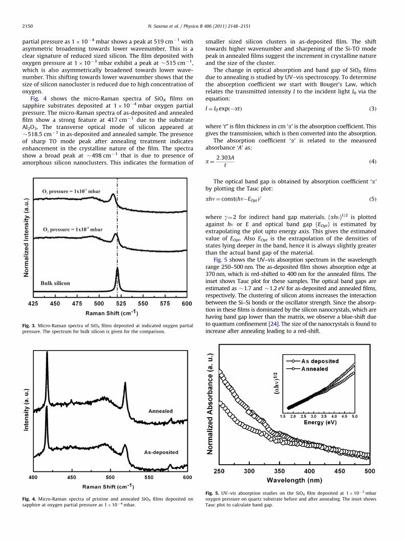
Fig. 4 shows the micro-Raman spectra of SiOX films onsapphire substrates deposited at 1�10�4 mbar oxygen partialpressure. The micro-Raman spectra of as-deposited and annealedfilm show a strong feature at 417 cm�1 due to the substrateAl2O3. The transverse optical mode of silicon appeared at�518.5 cm�1 in as-deposited and annealed sample. The presenceof sharp TO mode peak after annealing treatment indicatesenhancement in the crystalline nature of the film. The spectrashow a broad peak at �498 cm�1 that is due to presence ofamorphous silicon nanoclusters. This indicates the formation of
Fig. 3. Micro-Raman spectra of SiOX films deposited at indicated oxygen partial
pressure. The spectrum for bulk silicon is given for the comparison.
Fig. 4. Micro-Raman spectra of pristine and annealed SiOX films deposited on
sapphire at oxygen partial pressure as 1�10�4 mbar.
smaller sized silicon clusters in as-deposited film. The shifttowards higher wavenumber and sharpening of the Si-TO modepeak in annealed films suggest the increment in crystalline natureand the size of the cluster.
The change in optical absorption and band gap of SiOX filmsdue to annealing is studied by UV–vis spectroscopy. To determinethe absorption coefficient we start with Bouger’s Law, whichrelates the transmitted intensity I to the incident light I0 via theequation:
I¼ I0 expð�atÞ ð3Þ
where ‘t’’ is film thickness in cm ‘a’ is the absorption coefficient. Thisgives the transmission, which is then converted into the absorption.
The absorption coefficient ‘a’ is related to the measuredabsorbance ‘A’ as:
a¼ 2:303A
tð4Þ
The optical band gap is obtained by absorption coefficient ‘a’
by plotting the Tauc plot:
ahn¼ constðhn�EOptÞg
ð5Þ
where g¼2 for indirect band gap materials. (ahu)1/2 is plottedagainst hu or E and optical band gap (EOpt) is estimated byextrapolating the plot upto energy axis. This gives the estimatedvalue of EOpt. Also EOpt is the extrapolation of the densities ofstates lying deeper in the band, hence it is always slightly greaterthan the actual band gap of the material.
Fig. 5 shows the UV–vis absorption spectrum in the wavelengthrange 250–500 nm. The as-deposited film shows absorption edge at370 nm, which is red-shifted to 400 nm for the annealed films. Theinset shows Tauc plot for these samples. The optical band gaps areestimated as �1.7 and �1.2 eV for as-deposited and annealed films,respectively. The clustering of silicon atoms increases the interactionbetween the Si–Si bonds or the oscillator strength. Since the absorp-tion in these films is dominated by the silicon nanocrystals, which arehaving band gap lower than the matrix, we observe a blue-shift dueto quantum confinement [24]. The size of the nanocrystals is found toincrease after annealing leading to a red-shift.
Fig. 5. UV–vis absorption studies on the SiOX film deposited at 1�10�3 mbar
oxygen pressure on quartz substrate before and after annealing. The inset shows
Tauc plot to calculate band gap.

N. Saxena et al. / Physica B 406 (2011) 2148–2151 2151
The present studies show that the thermal annealing causesphase separation of the silicon suboxide formed during pulsedlaser ablation of silicon in oxygen environment. This suboxidefulfills the condition for spinodal decomposition and it is in ametastable state. The phase separation occurs when the localfluctuations in the concentration are activated thermally. Thisphase separation leads to enrichment of silicon rich and siliconpoor regions in the film viz. silicon rich regions become moresilicon rich and silicon poor regions become more silicon poor.This leads to increase in the size of the nanocrystals afterannealing. The oxygen content plays an important role in theformation of size selective nanoclusters in the film. The moreoxygen in the film reduces the silicon nanoclusters’ size. Thehigher concentration of silicon or lower amount of oxygen leadsto bigger size of nanoclusters in the film.
4. Conclusions
The effect of thermal annealing on the pulsed laser depositedfilms of silicon suboxide is studied. The silicon suboxide films ofdifferent compositions were deposited by varying the oxygen partialpressure in the chamber. The films deposited at lower oxygenpressure exhibit smaller nanocrystals size than the films depositedat higher oxygen pressure. The deposited silicon oxide films possesslocal fluctuations in concentration and separates into two phases,nanocrystalline silicon and SiO2, due to thermal activation. Thestudies show that the nanocrystals size can be controlled bydeposition parameters as well as post deposition annealing.
Acknowledgments
One of the authors (NS) is thankful to Inter University Accel-erator Center for providing funds in terms of fellowship. The helpreceived from Dr. D. M. Phase and Dr. Ram Janey Choudhary forpulsed laser deposition and Dr. Vasant Sathe for Raman
measurements from UGC-DAE Consortium for Scientific Research,Indore is gratefully acknowledged.
References
[1] C.A. Wang, R.K. Huang, D.A. Shiau, M.K. Connors, P.G. Murphy, P.W. Obrien,A.C. Anderson, D.M. DePoy, G. Nichols, M.N. Palmisiano, Appl. Phys. Lett. 83(7) (2003) 1286.
[2] H. Shibayama, S. Hasuo, T. Yamaoka, Appl. Phys. Lett. 47 (4) (1985) 429.[3] J.H. Magerlein, J.M. Baker, G.R. Proto, K.R. Grebe, S.P. Klepner, M.J. Palmer,
A.J. Warnecke, J. Vac. Sci. Technol B2 (4) (1984) 636.[4] M.S. Hedenqvist, K.S. Johansson, Surf. Coat. Technol 172 (1) (2003) 7.[5] K. Sato, T. Izumi, M. Iwase, Y. Show, H. Morisaki, T. Yaguchi, T. Kamino, Appl.
Surf. Sci. 216 (2003) 376.[6] L. Pavesi, L. Dal Negro, C. Mazzoleni, G. Franzo, F. Priolo, Nature 408 (2000)
440.[7] A.J. Kenyon, P.F. Trwoga, C.W. Pitt, J. Appl. Phys. 79 (12) (1996) 9291.[8] X.Y. Chen, Y.F. Lu, L.J. Tang, Y.H. Wu, B.J. Cho, X.J. Xu, J.R. Dong, W.D. Song,
J. Appl. Phys. 97 (2005) 014913.[9] H.Z. Song, X.M. Bao, N.S. Li, X.L. Wu, Appl. Phys. Lett. 72 (3) (1998) 356.
[10] Z. Lu, D.J. Lockwood, J.M. Baribeau, Nature 378 (1995) 258.[11] M. Benyoucef, M. Kubell, J.M. Sun, G.Z. Zhong, X.W. Fan, J. Appl. Phys. 89 (12)
(2001) 7903.[12] S. Yerci, U. Serincan, I. Dogan, S. Tokay, M. Genisel, A. Aydinli, R. Turan,
J. Appl. Phys. 100 (2006) 074301.[13] L. Patrone, D. Nelson, V.I. Safarov, M. Sentis, W. Marine, S. Giorgio, J. Appl.
Phys. 87 (8) (2000) 3829.[14] D. Riabinina, C. Durand, M. Chaker, F. Rasei, Appl. Phys. Lett. 88 (2006)
073105.[15] L.A. Nesbit, Appl. Phys. Lett. 46 (1) (1985) 38.[16] J.U. Schmidt, B. Schmidt, Mat. Sci. Eng. B 101 (2003) 28.[17] F. Rouchet, G. Dufour, H. Roult, B. Pelloie, J. Perriere, E. Fograssy, A. Slaoui,
M. Fronment, Phys. Rev. B 37 (1988) 6468.[18] P.S. Choudhary, T.M. Bhave, D. Kanjilal, S.V. Bhoaraskar, J. Appl. Phys. 93 (6)
(2003) 3486.[19] W.M. Arnoldbik, N. Tomozeiu, E.D. van Hattum, R.W. Lof, A.M. Verdenberg,
F.H.P.M. Habraken, Phys. Rev. B 71 (2005) 125329.[20] A. Barranco, J.A. Mejias, J.P. Espinnos, A. Cabellero, A.R. Gonzalez-Elipe,
F. Yubero, J. Vac. Sci. Technol., A 19 (2001) 136.[21] D.V. Tsu, G. Lucovsky, B.N. Davidson, Phys. Rev. B 40 (3) (1989) 1795.[22] A. Slaoui, E. Fogarassy, C. Fuchs, P. Siffert, J. Appl. Phys. 71 (2) (1992) 590.[23] Z. Iqbal, S. Veprek, J. Phys. C.: Solid State Phys. 15 (1982) 377.[24] Z. Xinwei, S. Olaf, K. Shuji, A. Yoshinobu, S. Takuo, Phys. Rev. B 50 (1994)
18654.