effects of dead zones in multiple-quantum-well binary-phase modulators on optical interconnections
TRANSCRIPT

Effects of dead zones in multiple-quantum-wellbinary-phase modulators on optical interconnections
Hanni Inbar and Mohammad R. Taghizadeh
We investigate the effects of inactive regions @dead zones ~DZ’s!# in multiple-quantum-well binary-phasemodulators used for free-space dynamic optical interconnection applications. Results, however, haveimplications for other types of pixelated spatial light modulators ~SLM’s!. To our knowledge, the effectsof DZ’s in SLM’s have not before been thoroughly studied in a context other than optical correlation. Weinvestigate the DZ’s ~considered to be either opaque or transmissive! as a feature that may be exploitedin system design, calculating light efficiency and fidelity as a function of DZ fractional width. It is shownthat in particular cases an appropriate choice of DZ width would lead to an optical interconnection withsubstantially improved cross-talk performance. © 1998 Optical Society of America
OCIS codes: 200.4650, 230.6120, 100.1390.
1. Introduction
Spatial light modulators ~SLM’s! are the key to therealization of real-time optical systems. An electri-cally addressed SLM is usually constructed with apixel structure, with each pixel consisting of two re-gions. The active zone ~AZ! is the region that en-codes the electric signal, thereby modulating thecomplex amplitude of the incident light. Its fractionof pixel area is called the pixel fill factor. The re-maining inactive region of the pixel is called the deadzone ~DZ!. A DZ is referred to as an opaque deadzone ~ODZ! if it completely blocks out any light inci-dent upon it, whereas it may be referred to as atransmissive dead zone ~TDZ! if it completely trans-mits ~or reflects! the light.1 Examples of SLM’swhose DZ’s are either opaque or transmissive ~reflec-tive! are listed in Ref. 1. Other devices having morecomplicated DZ’s could be modeled approximatelywith the assumption of an average value of the com-plex amplitude transmittance.1
The effects of SLM DZ’s were previously investi-gated in the context of optical-correlation systems.A few investigators2–4 have studied how pixelationand DZ’s in real SLM’s, such as deformable-mirrordevices and magneto-optic SLM’s, affect correlation.
The authors are with the Department of Physics, Heriot-WattUniversity, Edinburgh EH14 4AS, United Kingdom.
Received 2 June 1997; revised manuscript received 23 October1997.
0003-6935y98y050912-09$10.00y0© 1998 Optical Society of America
912 APPLIED OPTICS y Vol. 37, No. 5 y 10 February 1998
In each case evaluations were limited to one partic-ular configuration of DZ’s peculiar to the type of SLMconsidered. General calculations were performed byGianino and Woods,1,5,6 who studied frequency-planecorrelators that contain input and filter SLM’s whoseDZ’s are either opaque5 or transmissive.1,6 ForODZ’s one of their conclusions was that energy lossesare caused not only by ODZ blocking but also bydiffraction into off-axis replicated images.5 Theyhave also shown that the presence of TDZ’s intro-duces severe noise into the correlation pattern, re-sulting in false correlation peaks, additionalbackground patterns, and a signal-to-noise ratio thatdepends on the correlator design.1,6 Davis et al.7discuss a number of anomalies that can result in theoutput of a joint Fourier transform correlator whenthe joint power spectrum is written onto a SLM hav-ing a grid structure, thus showing that this structurecan cause spurious output cross-correlation peaksand can affect the strengths of the desired cross-correlation peaks.
To our knowledge, no investigators have thor-oughly studied the effects of SLM DZ’s in a contextother than optical correlation. In this paper westudy these effects in SLM’s used for free-space dy-namic optical interconnection applications. More-over, here the SLM DZ’s are investigated as a featurethat may be exploited, rather than merely as a draw-back that has to be taken into consideration. Theapplications of optical interconnection systems are inthe fields of digital optical processors and parallelelectronic machines, exploiting the high degree ofconnectivity offered by free-space optics. We chose

to consider the general application of 2 3 1 fan-outinterconnection patterns, which is the basis of manyoptical-computing topologies, e.g., perfect shuffle andBanyan.
Diffraction gratings implemented on a SLM canproduce these dynamic optical interconnections, asshown schematically in Fig. 1. The angle u betweenthe 11 ~or 21! diffraction order and the optical axis iscontrolled by the specific modulation pattern ~num-ber of pixels per period! encoded by the SLM. Gen-erally, the two major concerns regarding the qualityof optical interconnections are light efficiency andfidelity. Fidelity can be measured by means of theuniformity of the desired array and by means of crosstalk, i.e., light directed toward undesired orders.We calculate these performance criteria as functionsof the DZ fractional width. First, the DZ’s are con-sidered to be opaque. Then we also describe theadditional effects of the TDZ’s, as manifested in theresulting diffraction patterns. The SLM consideredhere is the multiple-quantum-well ~MQW! binary-phase modulator.8–11 Results, however, may be ap-plicable to other pixelated binary-phase SLM’s~modulation levels of 11 and 21!. We show that, forthe 2 3 1 fan-out application, the DZ’s may lead insome cases to diffraction patterns with substantiallyhigher fidelity, at the expense of lower light effi-ciency. This is significant since, for many intercon-nection systems, cross talk may be an extremelydetrimental factor.
2. Multiple-Quantum-Well Binary-Phase Modulator
In this section the MQW binary-phase modulator isdescribed. Although typical vertical-cavity Fabry–Perot optical modulators are amplitude switches,Trezza and Harris8 demonstrated that it is possible tomake a vertical-cavity phase-flip modulator thatmaintains the same reflected amplitude between theOFF and the ON states but that varies the reflectedphase between 0° and 180° when an electric field isapplied across the device. This binary-phase modu-lator is based on a quantum-well system in an opti-mized Fabry–Perot cavity. The quantum-wellsystem provides a large absorption change with zeroparasitic refractive-index change between the ON and
Fig. 1. Geometry of 2 3 1 fan-out interconnections.
the OFF states at the defined wavelength and voltageswing, whereas the Fabry–Perot cavity is designed toalternate, when switched, the dominant mirror re-sponsible for reflection. In contrast to waveguidedevices, the vertical-cavity devices could be placedinto large arrays. Such MQW binary-phase modu-lator arrays should have applications for stackableoptical switching and logic and high-efficiency spatiallight modulation.8
An electrically controlled first-order binary-phasediffraction grating was reported experimentally byTrezza and Harris,9 who used a one-dimensional~1-D! array of MQW binary-phase modulators. Herebias was applied only to alternating stripes. Theresulting diffraction grating reflects normally inci-dent light primarily into the first-order diffractionpeaks, thus producing one specific 2 3 1 fan-out in-terconnection pattern. Such phase diffraction grat-ings could be highly efficient, compared with similardiffraction gratings for which amplitude modulatorsare used. Trezza and Harris9 indicate that speedsas high as 100 GHz might be realized for individualstripes, since the structures are simple reverse-biased diodes with minimal carrier injection. Theyalso depicted the parasitic effects of sidewall etchingand device spacing on the far-field light distribution.The tapered grating sidewalls result from the wetchemical etchant used for defining the grating.9Evaluations were not general, but they were limitedto one particular configuration without considerationof the inactive-region properties as design parame-ters.
Preliminary studies have recently been con-ducted concerning the design and fabrication of a1-D array of independently controlled MQW binary-phase modulators ~830-nm wavelength of opera-tion!.10,11 Diffraction gratings implemented onsuch an array of independently controlled stripescould produce a variety of 2 3 1 fan-out intercon-nection patterns, with the angle u ~Fig. 1! beingcontrolled by the specific grating function. Oneimportant design issue for this array concerns theproperties of the inactive regions between the activestripes. This issue constitutes the subject of thispaper. Results of a mathematical analysis are pre-sented.
3. Modulator Structure
The 1-D array of independently controlled MQWbinary-phase modulators is shown in Fig. 2~a!.The photograph shows 32 fingers ~12-mm fingerspacing! in the center and the contact pads aboveand below the fingers ~for more details see Ref. 11!.A schematic drawing of the 1-D structure, whichshows three fingers, is presented in Fig. 2~b!. Letus denote by a and b the SLM pixel ~finger! spacingand the width of the DZ in each pixel, respectively.The DZ fractional width bya is denoted by fDZ,which lies within the interval @0, 1#, with fDZ 5 0corresponding to a SLM without DZ’s. The SLMpixel fill factor is ~1 2 fDZ!. Arrays of Fabry–PerotMQW modulators that exhibit an excellent unifor-
10 February 1998 y Vol. 37, No. 5 y APPLIED OPTICS 913

mity between devices, with a thickness variation of0.07% across an array, were reported.12 Here, forsimplicity, it is assumed that the uniformity of mod-ulators within an array is perfect. Thus the signalimpressed on the AZ of each individual SLM pixel ismodeled as being a constant value ~either 11 or 21!spread across the entire active area. For the DZ’s,the complex amplitude transmittance is denoted byT 5 A exp~if!, with A 5 0 ~A 5 1! corresponding toODZ’s ~TDZ’s!.
In the analysis discussed in Section 4, the array ofMQW binary-phase modulators is considered to beencoding one of two specific designs for the generalapplication of 2 3 1 fan-out interconnections: aperiodic modulation pattern of 2 fingersyperiod~11, 21! and a periodic modulation pattern of4 fingersyperiod ~11, 11, 21, 21!. For simplicity,infinitely periodic modulation patterns are assumed.In Section 4 the effects of DZ’s on optical intercon-nection quality are described for the two specific de-signs indicated above.
Fig. 2. One-dimensional array of MQW binary-phase modulators:~a! Photograph. ~b! Schematic drawing showing three pixels ~fin-gers!.
914 APPLIED OPTICS y Vol. 37, No. 5 y 10 February 1998
4. Analysis
To present the potential advantages of DZ’s betweenactive modulating zones let us first consider the arrayof MQW binary-phase modulators to be encoding the2-fingeryperiod ~11, 21! infinitely periodic modula-tion function. Initially we describe the case of ODZ’s~T 5 0!, and then we introduce the additional effectsof DZ’s having a complex amplitude transmittanceT 5 A exp~if!.
The amplitude-transmittance function for a 1-D ar-ray of binary-phase modulators with ODZ’s ~ fDZ 5bya! is ternary, as shown in Fig. 3~a!. For an arrayof binary-phase modulators without DZ’s ~ fDZ 5 0!,the amplitude transmittance is represented by thebinary-phase function depicted in Fig. 3~b!. Quali-tatively the effects of the ODZ’s may be interpreted inone of two ways. Although the two approaches areequivalent, they differently describe the manner inwhich the diffraction pattern of the array is affected.In the first approach, the ternary grating of Fig. 3~a!is considered to be the multiplication of the binarygrating of Fig. 3~b! by an appropriate binary-amplitude function. When the diffraction pattern ofthe ternary grating of Fig. 3~a! is considered, it fol-lows that the existence of ODZ’s results in an inter-ference between an infinite number of patterns,which are weighted and shifted replicas of the dif-fraction pattern of the binary grating of Fig. 3~b!. Inthe second approach, the ternary grating of Fig. 3~a!is considered to be the sum of the binary grating ofFig. 3~b! and an appropriate ternary function. Ac-cording to this latter approach, the diffraction pat-tern of the ternary grating of Fig. 3~a! may bedescribed by an interference between only two dif-fraction patterns.
Fig. 3. Amplitude transmittance of a binary-phase modulatorarray encoding a 2-fingeryperiod modulation pattern: ~a! Arraywith ODZ’s ~ fDZ 5 bya!. ~b! Array without DZ’s ~ fDZ 5 0!.

When the scalar-diffraction theory is considered,the amplitude of each order of the diffraction patternat the Fourier plane can be obtained when the Fou-rier series of the infinitely periodic grating is calcu-lated. For the general case of Fig. 3~a! one gets
G~x, fDZ 5 bya!uT50
52p (
n~odd!51
` Fcos~npfDZ! 1 1n
sinSnpxaD
1sin~npfDZ!
ncosSnp
xaDG , (1)
where the fractional width of the DZ’s ~ fDZ! is a pa-rameter. For the function of Fig. 3~b!, the Fourierseries calculation yields
G~x, fDZ 5 0! 54p (
n~odd!51
` 1n
sinSnpxaD . (2)
From Eqs. ~1! and ~2! it follows that the correspond-ing light-field distribution at the Fourier plane, i.e.,the diffraction pattern, contains odd orders only.
The diffraction efficiency hinc~ fDZ!, defined as thefraction of incident light that is directed to the 61orders, is
hinc~ fDZ! 54p2 @1 1 cos~pfDZ!#. (3)
One can also consider an effective diffraction effi-ciency heff~ fDZ! that takes into account the lighttransmitted by the SLM rather than the light inci-dent upon it, and this efficiency is given by
heff~ fDZ! 54p2
@1 1 cos~pfDZ!#
~1 2 fDZ!. (4)
The fraction of incident light that is transmitted bythe SLM is equal to the SLM pixel fill factor, since theAZ windows of the pixels are considered to be com-pletely transmissive and the DZ’s are assumed to beopaque. The effective diffraction efficiency becomesthe sole relevant value in the case in which a micro-lens array is appropriately fixed; this overcomes thelosses in the ODZ’s because it focuses all the incidentlight through the AZ windows of the pixels.13
With respect to fidelity, one is interested only incross-talk performance since, for real-valued modu-lation patterns, the diffraction intensity pattern issymmetric, i.e., the 11-order and the 21-order uni-formity is perfect. The intensity ratio of the firstorder to the nth order, denoted by Iratio
~1,n!~ fDZ!, is
I ratio~1,n!~ fDZ! 5 n2 @1 1 cos~pfDZ!#
@1 1 cos~npfDZ!#, (5)
where n is an odd number n 5 3, 5, . . .. For thespecific case of fDZ 5 0 ~binary-phase modulatorarray without DZ’s!, the intensity ratio of the firstto the nth diffraction order is Iratio
~1,n! ~0! 5 n2. Theabove results are illustrated in Figs. 4 and 5. Fig-ure 4 depicts the diffraction efficiencies @hinc~ fDZ!
and heff ~ fDZ!#, whereas Figs. 5~a!–5~d! showIratio
~1,3! ~ fDZ!, Iratio~1,5! ~ fDZ!, Iratio
~1,7! ~ fDZ!, and Iratio~1,9! ~fDZ!, re-
spectively.It can readily be shown that Iratio
~1,n! ~ fDZ! goes toinfinity for a finite set of fDZ values $ fDZ
~k! 5 kyn%, withk being the finite set of odd numbers $k 5 1, . . . ,n 2 2%. The value for fDZ should be chosen from thisset when cross-talk specifications concern mainly thevanishing of a specific nth order. As an example, thethird order is completely eliminated from the diffrac-tion pattern when fDZ 5 1y3. For the 61 orders,hinc~1y3! 5 0.608, whereas heff~1y3! 5 0.912. Thecorresponding modulator array without DZ’s yieldshinc~0! 5 heff~0! 5 0.811 but demonstrates a ratherpoor first- to third-order intensity ratio @Iratio
~1,3! ~0! 5 9#.Note also that, even though one third of the incidentlight power is blocked by the ODZ’s, the decrease indiffraction efficiency of the 61 orders is only approx-imately one quarter ~1 2 0.608y0.811!. This is amanifestation of the higher effective diffraction effi-ciency exhibited by the modulator array with DZ’s inthis example: A higher fraction of the light passingthe modulator is directed toward the 61 orders whileless light is directed to the other orders. A lowervalue of fDZ leads to a better diffraction efficiency andstill represents a Iratio
~1,3! higher than 9.When all undesired diffraction orders are consid-
ered to be equally detrimental in cross-talk specifica-tions, a different value for fDZ should be chosen.Here one should choose the value of fDZ for whichmin$Iratio
~1,n!% is the highest. Figure 6 depictsmin$Iratio
~1,n!% ~where n is any odd number $n 5 3, 5, . . .%!as a function of fDZ, indicating for each segment of thecurve the specific undesired nth diffraction order re-sponsible for limiting the performance. For exam-ple, the worst cross talk for low fDZ values is exhibitedby the order n 5 3. It can be shown that fDZ 5 0.248presents the best performance with respect to thesespecifications, maximizing min$Iratio
~1,n!~ fDZ!%. Here,min$Iratio
~1,n! ~0.248!% 5 50.14, thus representing a sig-nificant improvement in cross-talk performance ~by afactor of 5.57! over the case of a modulator array
Fig. 4. Two-fingeryperiod modulation pattern with ODZ’s. Theincident diffraction efficiency hinc~ fDZ! and the effective diffractionefficiency heff ~ fDZ! are shown.
10 February 1998 y Vol. 37, No. 5 y APPLIED OPTICS 915
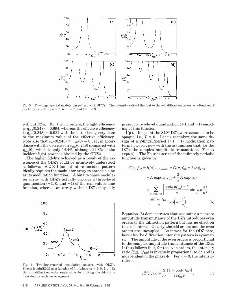
Fig. 5. Two-fingeryperiod modulation pattern with ODZ’s. The intensity ratio of the first to the nth diffraction orders as a function offDZ for ~a! n 5 3, ~b! n 5 5, ~c! n 5 7, and ~d! n 5 9.
without DZ’s. For the 61 orders, the light efficiencyis hinc~0.248! 5 0.694, whereas the effective efficiencyis heff~0.248! 5 0.922 with the latter being very closeto the maximum value of the effective efficiency.Note also that heff~0.248! . heff~0! 5 0.811, in accor-dance with the decrease in hinc~0.248! compared withhinc~0!, which is only 14.4%, although 24.8% of theincident light power is blocked by the ODZ’s.
The higher fidelity achieved as a result of the ex-istence of the ODZ’s could be intuitively understoodas follows: A 2 3 1 fan-out interconnection patternideally requires the modulator array to encode a sineas its modulation function. A binary-phase modula-tor array with ODZ’s actually encodes a three-levelquantization ~11, 0, and 21! of the real-valued sinefunction, whereas an array without DZ’s may only
Fig. 6. Two-fingeryperiod modulation pattern with ODZ’s.Shown is min$Iratio
~1,n!% as a function of fDZ ~where $n 5 3, 5, 7, . . . %!;the nth diffraction order responsible for limiting the fidelity isindicated for each curve segment.
916 APPLIED OPTICS y Vol. 37, No. 5 y 10 February 1998
present a two-level quantization ~11 and 21! encod-ing of this function.
Up to this point the SLM DZ’s were assumed to beopaque, i.e., T 5 0. Let us reanalyze the same de-sign of a 2-fingeryperiod ~11, 21! modulation pat-tern, however, now with the assumption that, for theDZ’s, the complex amplitude transmittance T 5 Aexp~if!. The Fourier series of the infinitely periodicfunction is given by
G~x, fDZ 5 bya!uT5Aexp~if! 5 G~x, fDZ 5 bya!uT50
1 A exp~if! fDZ 12p
A exp~if!
3 (n~even!52
` Fcos~npfDZ! 2 1n
sinSnpxaD
1sin~npfDZ!
ncosSnp
xaDG . (6)
Equation ~6! demonstrates that assuming a nonzeroamplitude transmittance of the DZ’s introduces evenorders to the diffraction pattern but has no effect onthe odd orders. Clearly, the odd orders and the evenorders are uncoupled. As it was for the ODZ case,here also the diffraction intensity pattern is symmet-ric. The amplitude of the even orders is proportionalto the complex amplitude transmittance of the DZ’s.It thus follows that, for the even orders, the intensityratio Iratio
~1,n! ~ fDZ! is inversely proportional to A2 and isindependent of the phase f. For n 5 0, the intensityratio is
I ratio~1,0! ~ fDZ! 5
2A2
@1 1 cos~pfDZ!#
~pfDZ!2 , (7)
Fig. 7. Two-fingeryperiod modulation pattern with TDZ’s ~A 5 1!. Shown are the intensity ratios of the first to the nth diffraction ordersas functions of fDZ for ~a! n 5 0, ~b! n 5 2, ~c! n 5 4, ~d! n 5 6, and ~e! n 5 8.
whereas for the even diffraction orders n 5 2, 4, . . . ,it is given by
I ratio~1,n!~ fDZ! 5
n2
A2
@1 1 cos~pfDZ!#
@1 2 cos~npfDZ!#. (8)
Figures 7~a!–7~e! show Iratio~1, 0!~ fDZ!, Iratio
~1,2!~ fDZ!, Iratio~1,4!
~ fDZ!, Iratio~1,6!~ fDZ!, and Iratio
~1,8!~ fDZ!, respectively, for abinary-phase modulator array with TDZ’s, i.e., A 5 1.It can be shown that, for any value of fDZ, min$Iratio
~1,n!%~where $n 5 0, 2, . . . %! is presented by the 0th dif-fraction order, with the value of min$Iratio
~1, 0!~ fDZ!% beinginversely proportional to A2. It follows that, to re-main above the cross-talk performance demonstratedby the odd orders, there exists a maximal allowedlevel of A for each value of fDZ. For the case of fDZ 50.248, discussed above, this level is A 5 0.3356,which means that, as long as the amplitude trans-mittance of the DZ’s is lower than 0.3356, the cross-talk performance will not be worse than that dictatedby the odd orders @min$Iratio
~1,n!~0.248!% 5 50.14#.Let us now consider the second design for the
general application of 2 3 1 fan-out interconnec-tions in which the SLM is encoding the 4-fingeryperiod ~11, 11, 21, 21! periodic modulationpattern, rather than the 2-fingeryperiod pattern in-vestigated up to this point. For a modulator array
with ODZ’s the diffraction pattern consists of oddorders only. Results are illustrated in Figs. 8 and9, which depict, respectively, the diffraction effi-ciencies and the intensity ratios for some odd dif-fraction orders. It can be shown that, when DZ’sare opaque, the diffraction order n 5 3 demon-strates the worst cross-talk performance ~for anyvalue of fDZ!. Assuming TDZ’s rather than ODZ’s
Fig. 8. Four-fingeryperiod modulation pattern with ODZ’s. Theincident diffraction efficiency hinc~ fDZ! and the effective diffractionefficiency heff ~ fDZ! are shown.
10 February 1998 y Vol. 37, No. 5 y APPLIED OPTICS 917

Fig. 9. Four-fingeryperiod modulation pattern with ODZ’s. Shown are the intensity ratios of the first to the nth diffraction orders asfunctions of fDZ for ~a! n 5 3, ~b! n 5 5, ~c! n 5 7, and ~d! n 5 9.
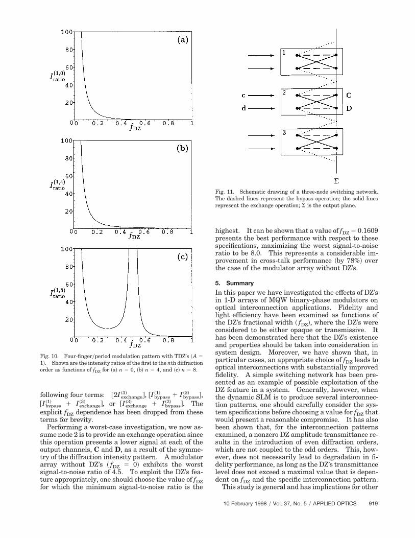
introduces the even orders $n 5 0, 4, 8, . . . % to thediffraction pattern. The intensity ratios Iratio
~1,n!~ fDZ!for n 5 0, n 5 4, and n 5 8 are shown in Fig. 10.Similar to the first design of 2 fingersyperiod,min$Iratio
~1,n!% ~where $n 5 0, 4, 8, . . .%! for any value offDZ is presented by the 0th diffraction order.
As an example of application of our analysis, webriefly describe a simple high-speed switching net-work that could be implemented by use of a 1-D arrayof independently controlled MQW binary-phase mod-ulators. This description is not intended to providea complete design of a switching network but ratherto demonstrate a possible exploitation of the DZ fea-ture in a system.
Figure 11 schematically depicts a switching-network system consisting of three independentexchange–bypass nodes. The nodes spacing is asindicated on the output plane S. Consider, for ex-ample, the operation of node 2 ~input channels c andd, output channels C and D!. Here light should bedirected from c to C and from d to D in the case of abypass process, whereas in the case of an exchangeprocess light should be directed from c to D and fromd to C. These two interconnection patterns could beproduced by use of a 1-D subarray of binary-phasemodulators for each node. The bypass operation~the dashed lines in Fig. 11! would be achieved bythe encoding of the simple modulation function~11, 11, . . .!, for which incident light is primarilydirected to the 0th order. Note that the undesiredorders included in the diffraction pattern of this mod-ulation function were not designated in the figure.An exchange operation ~the solid lines in Fig. 11!could be produced by the periodic modulation patternof 2 fingersyperiod ~11, 21!. As described in detailin the analysis, the resulting ~symmetric! diffractionintensity pattern mainly consists of the 61 orders.
918 APPLIED OPTICS y Vol. 37, No. 5 y 10 February 1998
Thus in this case incident light is ~primarily! directedto two complementary orders rather than steered in asingle direction. In Fig. 11, for each input channelthe useful first order used for the exchange process isindicated by a solid line, whereas the ~undesired!complementary first order is denoted by a dotted line.For clarity, additional ~undesired! diffraction ordersof this periodic modulation function were left un-marked in the figure.
When ODZ’s are assumed, the intensity of the nthdiffraction order of the bypass process, denoted byIbypass
~n! ~ fDZ!, is given by
Ibypass~0! ~ fDZ! 5 ~1 2 fDZ!
2, (9)
for the desired 0th order, whereas for the undesireddiffraction orders n 5 1, 2, . . . it is
Ibypass~n! ~ fDZ! 5
1p2
sin2~npfDZ!
n2 . (10)
For the exchange process one can derive the intensityof the nth diffraction order Iexchange
~n! ~ fDZ! from Eqs.~3! and ~5! to be
Iexchange~n! ~fDZ! 5
2p2
@1 1 cos~npfDZ!#
n2 , (11)
where n is any odd number n 5 1, 3, 5, . . . .Let us consider the signal-to-noise ratio at either
one of the output channels of node 2. The signal atthe output channel is the intensity of the desireddiffraction order, resulting from the process producedat node 2. Noise is defined here as the intensity sumof the undesired diffraction orders that illuminate theoutput channel of node 2 as side results of the pro-cesses produced at the adjacent nodes 1 and 3. De-pending on which processes ~bypass or exchange! areproduced at nodes 1 and 3, this noise sum is one of the
following four terms: @2Iexchange~3! #, @Ibypass
~1! 1 Ibypass~2! #,
@Ibypass~1! 1 Iexchange
~3! #, or @Iexchange~3! 1 Ibypass
~2! #. Theexplicit fDZ dependence has been dropped from theseterms for brevity.
Performing a worst-case investigation, we now as-sume node 2 is to provide an exchange operation sincethis operation presents a lower signal at each of theoutput channels, C and D, as a result of the symme-try of the diffraction intensity pattern. A modulatorarray without DZ’s ~ fDZ 5 0! exhibits the worstsignal-to-noise ratio of 4.5. To exploit the DZ’s fea-ture appropriately, one should choose the value of fDZfor which the minimum signal-to-noise ratio is the
Fig. 10. Four-fingeryperiod modulation pattern with TDZ’s ~A 51!. Shown are the intensity ratios of the first to the nth diffractionorder as functions of fDZ for ~a! n 5 0, ~b! n 5 4, and ~c! n 5 8.
highest. It can be shown that a value of fDZ 5 0.1609presents the best performance with respect to thesespecifications, maximizing the worst signal-to-noiseratio to be 8.0. This represents a considerable im-provement in cross-talk performance ~by 78%! overthe case of the modulator array without DZ’s.
5. Summary
In this paper we have investigated the effects of DZ’sin 1-D arrays of MQW binary-phase modulators onoptical interconnection applications. Fidelity andlight efficiency have been examined as functions ofthe DZ’s fractional width ~ fDZ!, where the DZ’s wereconsidered to be either opaque or transmissive. Ithas been demonstrated here that the DZ’s existenceand properties should be taken into consideration insystem design. Moreover, we have shown that, inparticular cases, an appropriate choice of fDZ leads tooptical interconnections with substantially improvedfidelity. A simple switching network has been pre-sented as an example of possible exploitation of theDZ feature in a system. Generally, however, whenthe dynamic SLM is to produce several interconnec-tion patterns, one should carefully consider the sys-tem specifications before choosing a value for fDZ thatwould present a reasonable compromise. It has alsobeen shown that, for the interconnection patternsexamined, a nonzero DZ amplitude transmittance re-sults in the introduction of even diffraction orders,which are not coupled to the odd orders. This, how-ever, does not necessarily lead to degradation in fi-delity performance, as long as the DZ’s transmittancelevel does not exceed a maximal value that is depen-dent on fDZ and the specific interconnection pattern.
This study is general and has implications for other
Fig. 11. Schematic drawing of a three-node switching network.The dashed lines represent the bypass operation; the solid linesrepresent the exchange operation; S is the output plane.
10 February 1998 y Vol. 37, No. 5 y APPLIED OPTICS 919

types of pixelated SLM’s used for optical interconnec-tions. Note, however, that analysis would requirethe use of a rigorous electromagnetic theory14 for theSLM’s falling into a regime for which the scalar-diffraction theory yields inaccurate results. Thecondition of validity for scalar optics is either thefeature size or the period size of the diffractive ele-ment, depending on the specific modulation func-tion.15 The scalar accuracy declines as the relevantsize decreases and is no longer much greater than thewavelength of incident light, with a range of validitythat depends on the SLM parameters.15
References1. P. D. Gianino and C. L. Woods, “General treatment of spatial
light modulator dead-zone effects on optical correlation. I.Computer simulations,” Appl. Opt. 32, 6527–6535 ~1993!.
2. J. E. Cravatt and M. K. Giles, “An improved model of the TIdeformable mirror device,” in Advances in Optical InformationProcessing IV, D. R. Pape, ed., Proc. SPIE 1296, 110–124~1990!.
3. M. K. Giles, J. Taylor, N. Grijalva, and B. Gioannini, “Opticalimage correlation using a deformable mirror device: a feasi-bility study,” in Acousto-Optic, Electro-Optic, and Magneto-Optic Devices and Applications, J. A. Lucero, ed., Proc. SPIE753, 72–81 ~1987!.
4. B. D. Bock, T. A. Crow, and M. K. Giles, “Design considerationsfor miniature optical correlation systems that use pixelatedinput and filter transducers,” in Optical Information Process-ing Systems and Architectures II, B. Javidi, ed., Proc. SPIE1347, 297–309 ~1990!.
5. P. D. Gianino and C. L. Woods, “Effects of spatial light mod-ulator opaque dead zones on optical correlation,” Appl. Opt. 31,4025–4033 ~1992!.
920 APPLIED OPTICS y Vol. 37, No. 5 y 10 February 1998
6. P. D. Gianino and C. L. Woods, “General treatment of spatiallight modulator dead-zone effects on optical correlation. II.Mathematical analysis,” Appl. Opt. 32, 6536–6541 ~1993!.
7. J. A. Davis, E. A. Merrill, D. M. Cottrell, and R. M. Bunch,“Effects of sampling and binarization in the output of the jointFourier transform correlator,” Opt. Eng. 29, 1094–1100 ~1990!.
8. J. A. Trezza and J. S. Harris Jr., “Creation and optimization ofvertical cavity phase flip modulators,” J. Appl. Phys. 75, 4878–4884 ~1994!.
9. J. A. Trezza and J. S. Harris Jr., “Two-state electrically con-trollable phase diffraction grating using arrays of vertical-cavity phase flip modulators,” IEEE Photonics Technol. Lett. 8,1211–1213 ~1996!.
10. E. Serrano, M. P. Y. Desmulliez, S. M. Prince, H. Inbar, andB. S. Wherrett, “Multiple-quantum-well binary-phase modu-lators: design and tolerance analysis,” in Spatial Light Mod-ulators, Vol. 14 of OSA Trends in Optics and Photonics Series~Optical Society of America, Washington D.C., 1997!, pp. 125–127.
11. L. C. Wilkinson, S. M. Prince, M. P. Y. Desmulliez, and C. R.Stanley, “Fabrication and testing of a multiple quantum wellbinary phase modulator,” in Spatial Light Modulators, Vol. 14of OSA Trends in Optics and Photonics Series ~Optical Societyof America, Washington D.C., 1997!, pp. 114–116.
12. A. Jennings, P. Horan, B. Kelly, and J. Hegarty, “AsymmetricFabry–Perot device arrays with low insertion loss and highuniformity,” IEEE Photonics Technol. Lett. 4, 858–860 ~1992!.
13. N. McArdle and M. R. Taghizadeh, “Real-time reconfigurableinterconnections for parallel optical processing,” Opt. Rev. 2,189–193 ~1995!.
14. R. Petit, ed., Electromagnetic Theory of Gratings ~Springer-Verlag, Berlin, 1980!.
15. D. A. Pommet, M. G. Moharam, and E. B. Grann, “Limits ofscalar diffraction theory for diffractive phase elements,” J. Opt.Soc. Am. A 11, 1827–1834 ~1994!.