efficient data mapping and buffering techniques for ...€¦ · 40 efficient data mapping and...
TRANSCRIPT

40
Efficient Data Mapping and Buffering Techniques for Multilevel CellPhase-Change Memories
HANBIN YOON* and JUSTIN MEZA, Carnegie Mellon UniversityNAVEEN MURALIMANOHAR, Hewlett-Packard LabsNORMAN P. JOUPPI**, Google Inc.ONUR MUTLU, Carnegie Mellon University
New phase-change memory (PCM) devices have low-access latencies (like DRAM) and high capacities (i.e.,low cost per bit, like Flash). In addition to being able to scale to smaller cell sizes than DRAM, a PCM cell canalso store multiple bits per cell (referred to as multilevel cell, or MLC), enabling even greater capacity perbit. However, reading and writing the different bits of data from and to an MLC PCM cell requires differentamounts of time: one bit is read or written first, followed by another. Due to this asymmetric access process,the bits in an MLC PCM cell have different access latency and energy depending on which bit in the cell isbeing read or written.
We leverage this observation to design a new way to store and buffer data in MLC PCM devices. Whiletraditional devices couple the bits in each cell next to one another in the address space, our key idea is tologically decouple the bits in each cell into two separate regions depending on their read/write characteris-tics: fast-read/slow-write bits and slow-read/fast-write bits. We propose a low-overhead hardware/softwaretechnique to predict and map data that would benefit from being in each region at runtime. In addition, weshow how MLC bit decoupling provides more flexibility in the way data is buffered in the device, enablingmore efficient use of existing device buffer space.
Our evaluations for a multicore system show that MLC bit decoupling improves system performance by19.2%, memory energy efficiency by 14.4%, and thread fairness by 19.3% over a state-of-the-art MLC PCMsystem that couples the bits in its cells. We show that our results are consistent across a variety of workloadsand system configurations.
Categories and Subject Descriptors: B.3.1 [Memory Structures]: Semiconductor Memories; C.0 [ComputerSystems Organization]: General
General Terms: Design, Algorithms, Performance
Additional Key Words and Phrases: Multilevel cell, phase-change memory, main memory, performance,energy, data mapping, data buffering
ACM Reference Format:HanBin Yoon, Justin Meza, Naveen Muralimanohar, Norman P. Jouppi, and Onur Mutlu. 2014. Efficientdata mapping and buffering techniques for multilevel cell phase-change memories. ACM Trans. Architec.Code Optim. 11, 4, Article 40 (December 2014), 25 pages.DOI: http://dx.doi.org/10.1145/2669365
*H. Yoon is currently at Google Inc.**This work was performed while the author was at Hewlett-Packard Labs.This research was supported by NSF Awards 0953246, 1147397, 1212962, 1320531, the Intel Science andTechnology Center for Cloud Computing, the Semiconductor Research Corporation, and the Intel MemoryHierarchy Program.Authors’ address: 5000 Forbes Ave, Pittsburgh, PA 15213; emails: [email protected], [email protected],[email protected], [email protected], [email protected] to make digital or hard copies of part or all of this work for personal or classroom use is grantedwithout fee provided that copies are not made or distributed for profit or commercial advantage and thatcopies show this notice on the first page or initial screen of a display along with the full citation. Copyrights forcomponents of this work owned by others than ACM must be honored. Abstracting with credit is permitted.To copy otherwise, to republish, to post on servers, to redistribute to lists, or to use any component of thiswork in other works requires prior specific permission and/or a fee. Permissions may be requested fromPublications Dept., ACM, Inc., 2 Penn Plaza, Suite 701, New York, NY 10121-0701 USA, fax +1 (212)869-0481, or [email protected]© 2014 ACM 1544-3566/2014/12-ART40 $15.00
DOI: http://dx.doi.org/10.1145/2669365
ACM Transactions on Architecture and Code Optimization, Vol. 11, No. 4, Article 40, Publication date: December 2014.

40:2 H. Yoon et al.
1. INTRODUCTION
There is a growing demand in computing systems, from mobile phones to servers,for larger-capacity main memories at lower cost. Traditional main memories have beencomposed of dynamic random-access memory (DRAM), a technology that is predicted tobe difficult to scale to smaller cell sizes without greatly increasing energy consumption[The International Technology Roadmap for Semiconductors 2010]. To help addressthese trends, recent research has focused on the design and application of more scalableresistive memories [Raoux et al. 2008; Wong et al. 2010; Hosomi et al. 2005; Strukovet al. 2008]. In this work, we focus on one type of resistive memory, phase changememory (PCM), due to its potential to provide higher device capacity compared toDRAM [Lee et al. 2009, 2010b] and its ability to store multiple bits per cell (calledmultilevel cell, or MLC), which DRAM cannot.1
Prior work on PCM has focused primarily on device architectures and techniquesto enable improved endurance, reduced access latency, and lower write latency/energy,which are agnostic to the number of bits per cell [Zhou et al. 2009; Qureshi et al. 2009a;Cho and Lee 2009; Ipek et al. 2010; Schechter et al. 2010; Yoon et al. 2011; Qureshi et al.2009b; Lee et al. 2009; Qureshi et al. 2012; Lee et al. 2010a; Yoon et al. 2012; Meza et al.2012a]. While such techniques can be applied to both single- or multilevel cell PCM,they do not take advantage of two of the unique aspects of MLC PCM. First, MLC PCMcell data is written iteratively: one bit is written first, followed by another [Bedeschiet al. 2009; Nirschl et al. 2007]. Second, MLC PCM cell data is read sequentially: thevalue of one bit can be detected before another [Qureshi et al. 2010b].
Such characteristics create asymmetry in the latencies and energies required for readand write operations in MLC PCM—varying by 16% to 80% depending on the beforeand after states of the cell [Bedeschi et al. 2009; Nirschl et al. 2007; Joshi et al. 2011;Qureshi et al. 2010b]. Keeping cell access latency low for MLC PCM cells is especiallyimportant because it can be a critical bottleneck in accessing device data, accountingfor 99% of the overall device write latency and more than 95% of the overall deviceread latency [Qureshi et al. 2010a, 2010b; Lee et al. 2009], compared to other sources ofdelay such as the address and data wire routing (in contrast to devices like DRAM, inwhich cell access latency is small compared to address and data wire routing delays).
In this article, we leverage this asymmetry in the latencies and energies required forread and write operations in MLC PCM to design a new way to store and buffer datain MCL PCM devices. Our key idea is to logically decouple the bits in each cell into twoseparate regions depending on their read/write characteristics: fast-read/slow-write(FR) bits and slow-read/fast-write (FW) bits.2 Based on this key idea, our technique,called decoupled bit mapping (DBM), exposes to the system two logical regions in anMLC PCM device (using one control bit to differentiate between the two): (1) a regionwith low latency and low energy for reads (which uses the FR bits), and (2) a regionwith low latency and low energy for writes (which uses the FW bits).
We also propose a new low-overhead hardware/software technique to take advantageof a DBM-enabled MLC PCM device to make better page placement decisions (similarto the goal of Ramos et al. [2011], Yoon et al. [2012], and Dhiman et al. [2009]). Ourasymmetric page mapping (APM) technique uses a small set of hardware countersto track the read/write intensity of the most active load and store instructions in aprogram. When the operating system (OS) is about to allocate a new physical pagein MLC PCM, it queries a hardware structure with the address of the load or store
1Though we perform our quantitative evaluations using MLC PCM as an example device, our techniquesare applicable to other resistive memories with similar characteristics to MLC PCM.2Note that, concurrent to our work [Yoon et al. 2013], Jiang et al. [2012a] made a similar observation in thecontext of STT-RAM caches. In that article, FR bits are called RFWS bits and FW bits are called RSWF bits.
ACM Transactions on Architecture and Code Optimization, Vol. 11, No. 4, Article 40, Publication date: December 2014.

Efficient Data Mapping and Buffering Techniques for MLC PCM 40:3
instruction that initiated the page allocation, and receives a prediction of whetherthe page will be (1) read-intensive or (2) write-intensive. Pages predicted to be read-intensive are mapped to the FR region of a DBM-enabled MLC PCM device, whilepages predicted to be write-intensive are mapped to a device’s FW region.
Finally, we design a new technique that shows how the MLC bit decoupling enabledby DBM provides more flexibility in the way data is buffered in an MLC PCM device.Internally, memory devices buffer a small amount of data being read or written in astructure called the row buffer. Modern MLC PCM devices with coupled bit mappingsutilize a row buffer organization that joins together the bits of a cell in the row buffer.We show that by logically decoupling the bits of a cell with DBM, using the same rowbuffer space and only a small amount of additional control circuitry, we can split therow buffer space between two logically separate row buffers: a row buffer for FR bitsand a row buffer for FW bits. We show that our split row buffer (SRB) organizationenables more efficient use of existing device buffer space, similar to if row buffer spacehad been doubled, but without the large overhead.
We make the following contributions:
—A technique developed concurrently with Jiang et al. [2012a] for mapping the bits inMLC PCM cells that exposes to the system two logical regions: (1) a region with lowlatency and low energy for reads and (2) a region with low latency and low energy forwrites3. Unlike Jiang et al., who examined the applicability of their technique in thecontext of STT-RAM caches, we leverage and evaluate our technique in the contextof a PCM main memory.
—A hardware/software technique to predict and map data that would benefit frombeing in each DBM region at runtime based on its read/write characteristics. Tomake the prediction, we use a low-overhead hardware table to track the read/writecharacteristics of a small number of the most active load and store instructions.
—A new row buffer organization for MLC PCM devices, enabled by DBM, that provideslogically separate row buffers for each of the different bits in an MLC, with only asmall amount of additional control circuitry. We show that our SRB organizationenables more efficient use of existing device buffer space.
—An evaluation of our schemes for a multicore system showing that the combinationof our techniques improves system performance by 19.2%, memory energy efficiencyby 14.4%, and thread fairness by 19.3% over a state-of-the-art MLC PCM systemthat couples the bits in its cells. We show that our results are consistent across avariety of workloads and system configurations.
2. BACKGROUND
2.1. Memory Device Architecture
Memory devices consist of arrays of cells and peripheral circuitry. Figure 1 shows amemory device array, where cells are organized into rows and columns. All of the cellsin a row are connected to a common word line, and all of the cells in a column areconnected to a common bit line. To simplify the device organization, when accessingdata in the array, an entire row of cells is accessed simultaneously. To do this, a rowdecoder asserts a word line to select all of the cells in a target row, and the bit linestransmit data between the cells and peripheral circuits.
In the peripheral circuits, data signals from the bit lines are detected by senseamplifiers and latched in the row buffer, and a column decoder selects a subset of therow buffer to be transmitted to the I/O pads. Once a row’s data is placed in the row
3Though we focus on MLC PCM devices with two bits per cell, our technique can be generalized to supportdevices with more bits per cell.
ACM Transactions on Architecture and Code Optimization, Vol. 11, No. 4, Article 40, Publication date: December 2014.

40:4 H. Yoon et al.
Fig. 1. Memory cell array shown with PCM cells. S/A = sense amplifier.
Fig. 2. PCM cell resistance distribution.
buffer, subsequent data requests to the same row can be served by accessing the datain this buffer. Such an access is known as a row buffer hit, and can be served quickly atthe access latency of the row buffer without interacting with the slower cell array. Inorder to serve a data request to a different row, data must be accessed from the array(replacing the contents of the row buffer). This type of access is known as a row buffermiss, and incurs higher latency and higher energy consumption than a row buffer hitbecause it must perform the previously described steps to access a row of cells in thearray.
2.2. Phase Change Memory
Phase-change memory (PCM) is a memory technology that stores data in a cell by vary-ing the electrical resistance of a material called chalcogenide [Raoux et al. 2008; Wonget al. 2010]. By applying heat and then allowing it to cool at different rates, chalcogenidecan be manipulated to settle between an amorphous (quickly cooled) high-resistancestate, and a crystalline (slowly cooled) low-resistance state. Each state corresponds toa nonoverlapping resistance range, and the resistance of cells programmed to the samevalue falls into the same range, but their exact resistance could be different (due toprocess variation). For example, Figure 2(a) illustrates the distribution of cells withdifferent resistance values if all cells were programmed with the value 0 or the value 1.The nonoverlap space between the ranges is called the distribution margin. Becausethe physical state of each cell is modified when it is programmed, PCM is able to retainthe data stored in its cells in the absence of power, making it a nonvolatile memorytechnology.
ACM Transactions on Architecture and Code Optimization, Vol. 11, No. 4, Article 40, Publication date: December 2014.

Efficient Data Mapping and Buffering Techniques for MLC PCM 40:5
Compared to DRAM cells, which store data using electrical charges in a capacitor,PCM cells have been shown to be easier to shrink to smaller sizes [Wong et al. 2010].This gives PCM devices the potential to provide higher density, lower cost per bit,and larger capacity than DRAM [Lee et al. 2009]. In addition, PCM’s low static powerfurther adds to its competitiveness as a scalable DRAM alternative.
However, PCM exhibits several drawbacks compared to DRAM, as described by Leeet al. [2009]. Cell access latency may be 4 to 32× larger depending on the operation andcell access energy is around 2× for reads and 10 to 140× for writes compared to DRAM.PCM cells also may only be written around 106 to >109 times, compared to DRAM cells,which may be written an estimated 1017 times [The International Technology Roadmapfor Semiconductors 2010].
PCM devices are still in an early phase of development and deployment, andmany solutions have been proposed to overcome PCM’s shortcomings. Some proposalsinclude DRAM caching [Qureshi et al. 2009b], fine-grained buffering of row data [Leeet al. 2009], wear-leveling/-reduction [Qureshi et al. 2009a; Cho and Lee 2009; Zhouet al. 2009], and fault-tolerance techniques [Ipek et al. 2010; Schechter et al. 2010;Yoon et al. 2011].
2.3. Multilevel Cell Memory
Multilevel cell (MLC, or multibit cell) refers to a memory cell’s ability to store morethan one bit of data. Multiple bits can be stored in a PCM cell by programming andsensing additional resistance states. Figure 2(b) shows how two additional resistancestates could be added to a cell to enable it to encode two bits of data. As a result, MLCdevices can store more data per unit area compared to cells with only a single level.
Notice that compared to Figure 2(a), the range of resistances that correspond to eachstate is smaller, which requires more accurate programming and sensing. Due to this,MLC cells are read and written using techniques that have higher access latency andhigher access energy compared to cells with only a single level [Bedeschi et al. 2009;Nirschl et al. 2007; Qureshi et al. 2010b].
One challenge in the adoption of MLC memory devices is the phenomenon of resis-tance drift, which has been documented in PCM devices [Seong et al. 2013]; a similarissue has been identified in other MLC nonvolatile memories such as Flash [Cai et al.2012, 2013]. Resistance drift occurs when the resistance of a cell changes over timedue to disturbance caused by accessing nearby cells in a device or due to changes inthe cell material structure due to repeated accesses over time. Recent work [Seonget al. 2013] has examined ways to mitigate this effect by using the appropriate numberof resistance ranges for MLCs. We believe that such techniques can be used to helpmitigate the effects of resistance drift in MLC PCM devices and enable their reliableuse.
3. MOTIVATION
3.1. Cell Read/Write Asymmetries in MLC PCM
Due to the way that data is read from and written to MLC PCM cells, each bit in anMLC cell requires a different amount of latency and energy to read or write. We nextdescribe why these asymmetries occur and how we can leverage them to design moreefficient techniques to manage MLC PCM devices.
3.1.1. Cell Read Asymmetry. The read latency of an MLC PCM cell depends on the stateof the cell. This is illustrated in Figure 3(a), which depicts an MLC PCM read operationon a cell with four levels (corresponding to two bits of stored data). An integratinganalog-to-digital converter quantizes the resistance of an MLC PCM cell to a two-bitvalue (we refer to the left bit as the most significant bit, MSB, and the right bit as the
ACM Transactions on Architecture and Code Optimization, Vol. 11, No. 4, Article 40, Publication date: December 2014.

40:6 H. Yoon et al.
Fig. 3. MLC PCM cell read operation [Qureshi et al. 2010b].
least significant bit, LSB) by measuring the time taken to send an electrical currentfrom the bit line through the cell. A cell in a lower resistance state will take less time topropagate the current than a cell in a higher resistance state. Therefore, the contentsof a cell can be determined by monitoring the time it takes for the bit line voltage (Vbl inFigure 3(a)) to reach a reference voltage (Vref ). In Figure 3(a), it took t3 amount of timefor Vbl to reach Vref , thus the corresponding value of the MSB is 0 and the LSB is 1.
However, notice that some information is available about the contents of the cell evenbefore time t3. As Figure 3(b) shows, after time t2, we may eliminate the possibility ofthe cell contents being either 11 or 10, because if it contained either of these values,Vbl would have to be ≤Vref by time t2, which it is not. Since the only remaining valuesthat the cell may contain are 01 or 00, after time t2, it must be the case that the MSB(the left bit) is 0. Thus, due to cell read asymmetry, one of the bits in an MLC PCM cell(the MSB bit in our example) can be accessed with lower read latency and lower readenergy than the other.
This property of MLC PCM cells is not exploited in conventional architectures, how-ever, because all of the bits in each cell belong to the same block of data, thus mustalways be accessed together. In other words, in addition to being physically coupledtogether, the bits in MLC PCM cells in traditional architectures are also logically cou-pled together. By decoupling the bits in an MLC PCM cell, we can more efficiently readdata from one of the bits in the cell.
3.1.2. Cell Write Asymmetry. The write latency and write energy of an MLC PCM celldepend on (1) the initial state of the cell and (2) the final state of the cell. This isbecause transitioning a cell between the different resistance states in Figure 2(b)requires different amounts of power to be applied over different amounts of time. Thereare two techniques for programming PCM cells: (1) partially crystallizing amorphouschalcogenide and (2) partially amorphizing crystalline chalcogenide. MLC PCM writeoperation is optimized to use the faster of these two techniques for each transition[Nirschl et al. 2007; Happ et al. 2006; Joshi et al. 2011] provide more detail on theimplementation and application of these techniques.4
Figure 4(a) shows the amount of time taken to transition a two-bit MLC PCM cellbetween any two states (normalized to the slowest transition latency). There are two
4While it remains to be seen whether the programming techniques developed in these works will eventuallybecome the dominant type of programming scheme for MLC PCM cells, we note that other nonvolatilestorage technologies such as Flash have successfully adopted similar techniques (e.g., Suh et al. [1995]), andwe believe that nonvolatile memory devices will be able to do so as well.
ACM Transactions on Architecture and Code Optimization, Vol. 11, No. 4, Article 40, Publication date: December 2014.

Efficient Data Mapping and Buffering Techniques for MLC PCM 40:7
Fig. 4. MLC PCM cell write latencies [Joshi et al. 2011; Nirschl et al. 2007; Happ et al. 2006].
things to note in Figure 4(a): (1) the worst-case latencies among all the possible tran-sitions correspond to changing the value of the MSB (from 0 to 1, shown by the boldlines) and (2) the worst-case latency among all the possible transitions for changingthe LSB is only 0.84× (corresponding to changing the LSB from 0 to 1). This suggeststhat if we could isolate which of the bits in an MLC PCM cell we change at one time,we could guarantee lower write latency for LSB bit changes. Figure 4(b) shows the nor-malized state transition latency when a cell may change only its MSB (correspondingto vertical transitions) or its LSB (corresponding to horizontal transitions) but not bothin the same write operation. Applying this constraint shows that while the worst-casewrite latency for the MSB is 1.0×, the worst-case write latency for the LSB is boundedat 0.84×. Thus, due to cell write asymmetry, one of the bits in an MLC PCM cell (theLSB bit in our example) can be written with lower write latency and lower write energythan the other.
Similar to cell read asymmetry, this property of MLC PCM cells is also not exploitedin conventional architectures because all of the bits in a cell belong to the same block ofdata and must therefore always be modified together. By logically decoupling the bitsin an MLC PCM cell, we can more efficiently write data to one of the bits in the cell.
3.1.3. Key Observation. Notice from our discussion that the bit that provides the bestread latency and read energy (the MSB bit in our examples) is different from the bitthat provides the best write latency and write energy (the LSB bit in our examples).Our key observation is that the bits in an MLC PCM cell can be used in a way thatcomplement each other in terms of their read/write characteristics—a property thatwe propose to leverage. We hereafter refer to bits that provide the best read latencyand read energy as fast-read/slow-write (FR) bits, and bits that provide the best writelatency and write energy as slow-read/fast-write (FW) bits.
3.2. Leveraging Read/Write Asymmetry
We leverage MLC PCM cell read/write asymmetry to logically decouple the bits of eachcell to create two regions of memory: (1) a region composed of FR bits that is moreefficient for reading data and (2) a region composed of FW bits that is more efficientfor writing data. We call this technique decoupled bit mapping, or DBM. Note that asimilar mechanism was concurrently proposed for STT-RAM caches [Jiang et al. 2012a].The main contribution with respect to our technique is its evaluation in the context of
ACM Transactions on Architecture and Code Optimization, Vol. 11, No. 4, Article 40, Publication date: December 2014.
40:8 H. Yoon et al.
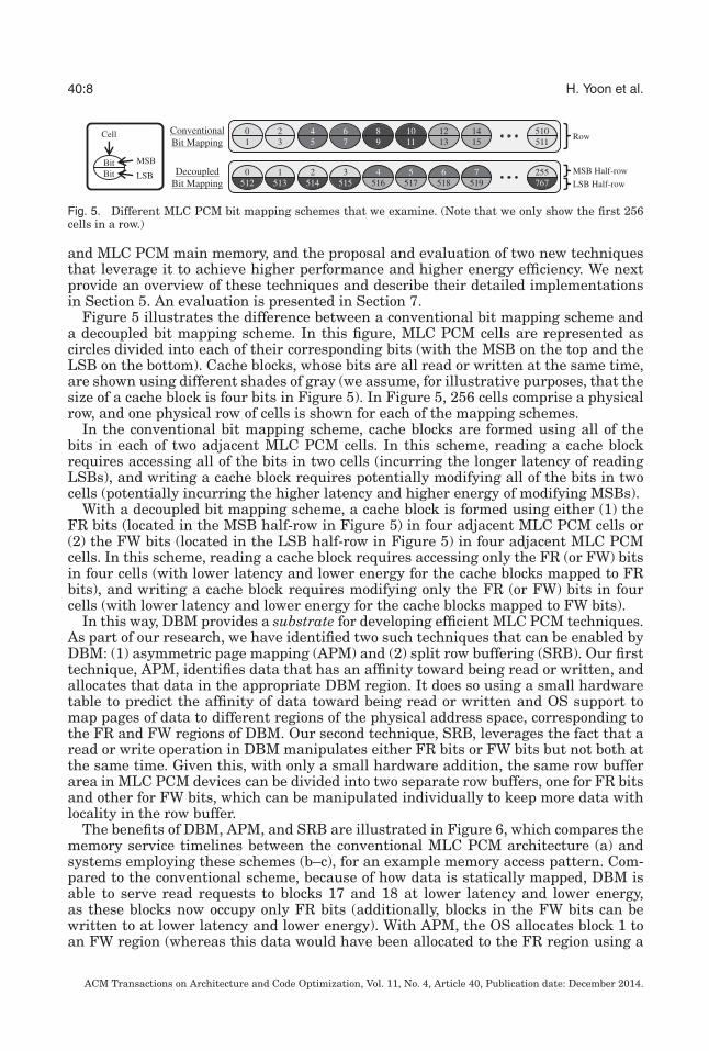
Fig. 5. Different MLC PCM bit mapping schemes that we examine. (Note that we only show the first 256cells in a row.)
and MLC PCM main memory, and the proposal and evaluation of two new techniquesthat leverage it to achieve higher performance and higher energy efficiency. We nextprovide an overview of these techniques and describe their detailed implementationsin Section 5. An evaluation is presented in Section 7.
Figure 5 illustrates the difference between a conventional bit mapping scheme anda decoupled bit mapping scheme. In this figure, MLC PCM cells are represented ascircles divided into each of their corresponding bits (with the MSB on the top and theLSB on the bottom). Cache blocks, whose bits are all read or written at the same time,are shown using different shades of gray (we assume, for illustrative purposes, that thesize of a cache block is four bits in Figure 5). In Figure 5, 256 cells comprise a physicalrow, and one physical row of cells is shown for each of the mapping schemes.
In the conventional bit mapping scheme, cache blocks are formed using all of thebits in each of two adjacent MLC PCM cells. In this scheme, reading a cache blockrequires accessing all of the bits in two cells (incurring the longer latency of readingLSBs), and writing a cache block requires potentially modifying all of the bits in twocells (potentially incurring the higher latency and higher energy of modifying MSBs).
With a decoupled bit mapping scheme, a cache block is formed using either (1) theFR bits (located in the MSB half-row in Figure 5) in four adjacent MLC PCM cells or(2) the FW bits (located in the LSB half-row in Figure 5) in four adjacent MLC PCMcells. In this scheme, reading a cache block requires accessing only the FR (or FW) bitsin four cells (with lower latency and lower energy for the cache blocks mapped to FRbits), and writing a cache block requires modifying only the FR (or FW) bits in fourcells (with lower latency and lower energy for the cache blocks mapped to FW bits).
In this way, DBM provides a substrate for developing efficient MLC PCM techniques.As part of our research, we have identified two such techniques that can be enabled byDBM: (1) asymmetric page mapping (APM) and (2) split row buffering (SRB). Our firsttechnique, APM, identifies data that has an affinity toward being read or written, andallocates that data in the appropriate DBM region. It does so using a small hardwaretable to predict the affinity of data toward being read or written and OS support tomap pages of data to different regions of the physical address space, corresponding tothe FR and FW regions of DBM. Our second technique, SRB, leverages the fact that aread or write operation in DBM manipulates either FR bits or FW bits but not both atthe same time. Given this, with only a small hardware addition, the same row bufferarea in MLC PCM devices can be divided into two separate row buffers, one for FR bitsand other for FW bits, which can be manipulated individually to keep more data withlocality in the row buffer.
The benefits of DBM, APM, and SRB are illustrated in Figure 6, which compares thememory service timelines between the conventional MLC PCM architecture (a) andsystems employing these schemes (b–c), for an example memory access pattern. Com-pared to the conventional scheme, because of how data is statically mapped, DBM isable to serve read requests to blocks 17 and 18 at lower latency and lower energy,as these blocks now occupy only FR bits (additionally, blocks in the FW bits can bewritten to at lower latency and lower energy). With APM, the OS allocates block 1 toan FW region (whereas this data would have been allocated to the FR region using a
ACM Transactions on Architecture and Code Optimization, Vol. 11, No. 4, Article 40, Publication date: December 2014.

Efficient Data Mapping and Buffering Techniques for MLC PCM 40:9
Fig. 6. Decoupled bit mapping can improve performance compared to a conventional bit mapping, with thepotential to further improve performance using asymmetric page mapping and split row buffering.
static mapping scheme). Thus, APM is able to exploit the lower write latency and writeenergy of FW bits to serve the write request to block 1. Serving the read request toblock 18 results in a row buffer miss access without SRB, as the row buffer will containthe row with the previously accessed block 10. However, with SRB, blocks 17 and 18can simultaneously be buffered in the row buffer, causing the read request to block18 (which is buffered along with block 17) to be a row buffer hit access. This furtherreduces the time and energy taken to serve the memory requests.
4. DETAILED MECHANISMS
4.1. Decoupled Bit Mapping (DBM)
DBM is designed to expose the lower latency and lower energy of FR bit reads andFW bit writes. To this end, the bits of an MLC cell are mapped to separate logicaladdresses, as illustrated in Figure 5. Whereas these bits are coupled to form a singlecontiguous memory address along a row in the conventional scheme, DBM groups theFR bits along a row to form one contiguous address, and groups the FW bits along thesame row to form another. This way, a data block (e.g., a 64B cache block) that residesat a certain logical address physically occupies only FR bits or only FW bits. If thedata block is in FR bits, read asymmetry is exploited to read the block at a reducedlatency and energy (the FR region). If the data block is in FW bits, write asymmetry isexploited to write to the block at a reduced latency and energy (the FW region).
DBM divides all rows in memory (i.e., all cells that share a common word line) intotwo logical regions: one consisting of FR bits, the other consisting of FW bits. Assuminga uniformly random translation from an application’s virtual page address to a physicalpage address in memory, approximately half of the application’s working set would bein FR bits and the other half in FW bits. Hence with DBM, on average, 50% of the datain memory may be served at reduced read latency (by 48%) and read energy (by 48%),and 50% of the data in memory may be served at reduced write latency (by 16%) andwrite energy (by 26%).
The downside of DBM is that it may increase the average number of cells that are pro-grammed during a write operation, potentially wearing out more cells more quickly.This is because, with DBM, a data block uses only one bit from each multibit cell,
ACM Transactions on Architecture and Code Optimization, Vol. 11, No. 4, Article 40, Publication date: December 2014.
40:10 H. Yoon et al.
potentially involving a number of cells equal to the number of bits in a block whenwriting to the block. However, this does not double the write endurance overhead com-pared to the conventional scheme, as the probability of redundant bit-writes [Zhouet al. 2009] (where the cell is already in the target state to be programmed to, thusavoiding a programming operation) is lower in the conventional scheme. For program-ming a cell to be redundant in the conventional scheme, both the FR bit and the FWbit have to match with the write data. On the other hand, write data to a block inDBM targets only FR bits or only FW bits. If the write is to FR bits, the FW bits areunchanged, and vice versa. Because only one bit per cell needs to match with the writedata in DBM, the probability of redundant bit-writes is higher in DBM than in theconventional scheme (also noted by Zhou et al. [2009] and Jiang et al. [2012b]), and weobserve on average a 28.2% endurance overhead in our results (discussed in Section7.4). As we will show, this is small enough to achieve a typical server operational life-time of 5 years (server installations typically have a lifetime of 3 to 4 years [Barrosoet al. 2013]), even assuming pessimistic PCM cell wearout characteristics.
By employing DBM, two separate logical address spaces share the row buffer space,with data from each address space occupying half of the row buffer. This reduces thelongest contiguous address space that can be held in the row buffer, potentially de-creasing row buffer locality. However, the reduced memory access latency and energyexposed by DBM have the potential to more than compensate for this effect, and sig-nificantly improve system performance and energy efficiency over the conventionalMLC PCM architecture, while not incurring any major modifications to the memorycircuitry (we detail our implementation in Section 5). To utilize read and write asym-metries more effectively, we next propose a technique to map a page to either the FRregion or FW region depending on the page’s memory read/write affinity.
4.2. Asymmetric Page Mapping (APM)
With DBM alone, it is not possible to ensure that a page will get mapped to the mostbeneficial region of memory in terms of reduced latency and energy. This is becauseonly half of the memory space is efficient in serving reads (the FR region), while theother half of memory is efficient in serving writes (the FW region), yet OS physical pageallocation may distribute pages arbitrarily between both regions (an effect we modelin our evaluations). However, many applications exhibit skewed page-access behaviorwhere a small fraction of pages account for a large portion of the memory accesses. Forexample, Table I shows this trend for SPEC CPU2006 benchmarks, listing the fractionof pages that account for 80% of the memory reads and 80% of the memory writes inthe second and third columns5. On average, 80% of the reads and writes are accountedfor by 41% and 22% of the pages, respectively.
To understand how reads and writes are distributed within pages, we examinedthe ratio of reads to writes (and writes to reads) for frequently accessed pages thatreceive 90% or more of the reads or writes in the program. The fourth column showsthe fraction of frequently read pages (those that service >90% of reads in the program)with a read-to-write ratio greater than 10. These pages are both frequently read andread-intensive. The fifth column shows the fraction of frequently written pages (thosethat service >90% of writes in the program) with a write-to-read ratio greater than 2 (ingeneral, the programs we examine are more read intensive than write intensive, so weadjust our standard for write intensity accordingly). These pages are both frequentlywritten and write-intensive. This fraction is greater than 80% for 17 benchmarks ineither reads or writes, indicating that many applications frequently access pages with
5In our evaluation, we examine workloads consisting of a subset of these benchmarks in addition to otherparallel and multithreaded workloads (see Section 6).
ACM Transactions on Architecture and Code Optimization, Vol. 11, No. 4, Article 40, Publication date: December 2014.

Efficient Data Mapping and Buffering Techniques for MLC PCM 40:11
Tabl
eI.
Rel
evan
tMem
ory
Acc
ess
Cha
ract
eris
tics
ofS
PE
CC
PU
2006
Ben
chm
arks
Fra
ctio
nof
acce
ssed
page
sth
atse
rve
Fra
ctio
nof
inst
ruct
ion
sth
atin
itia
lly
Ben
chm
ark
80%
ofre
ads
80%
ofw
rite
s>
10re
ads
per
wri
te>
2w
rite
spe
rre
adR
ead
apa
geW
rite
apa
gelb
m75
%75
%0%
100%
2%2%
libq
uan
tum
73%
<1%
100%
6%2%
2%bw
aves
70%
3%55
%1%
44%
40%
mil
c68
%37
%25
%43
%3%
4%G
emsF
DT
D63
%7%
94%
2%33
%6%
gobm
k60
%58
%9%
93%
9%8%
zeu
smp
60%
53%
40%
54%
37%
20%
cact
us
57%
26%
83%
84%
43%
23%
asta
r54
%55
%52
%98
%4%
2%n
amd
54%
39%
44%
100%
2%1%
lesl
ie3d
51%
32%
0%8%
20%
12%
omn
etpp
46%
22%
63%
1%13
%11
%gc
c44
%22
%81
%70
%11
%8%
sjen
g40
%26
%27
%5%
3%3%
sph
inx3
39%
1%88
%29
%12
%4%
grom
acs
38%
23%
36%
36%
22%
11%
perl
ben
ch36
%8%
80%
77%
54%
84%
calc
uli
x24
%3%
95%
8%4%
1%de
alII
23%
26%
15%
60%
9%9%
gam
ess
22%
7%99
%45
%7%
2%po
vray
22%
4%65
%27
%44
%11
%so
plex
20%
10%
17%
35%
18%
16%
h26
4ref
19%
15%
0%11
%22
%21
%bz
ip2
17%
10%
54%
100%
7%4%
hm
mer
17%
16%
0%10
0%3%
3%xa
lan
cbm
k12
%1%
99%
9%20
%18
%m
cf7%
<1%
100%
1%2%
2%A
vera
ge41
%22
%53
%45
%17
%12
%
ACM Transactions on Architecture and Code Optimization, Vol. 11, No. 4, Article 40, Publication date: December 2014.
40:12 H. Yoon et al.
a strong bias toward reads or writes. Thus, by identifying and placing these access-intensive pages in memory regions that can efficiently serve the type of access (read orwrite) the pages frequently receive, it is possible to serve a larger portion of memoryrequests at reduced latency and energy.
There are two main approaches to achieving this page placement: reactive migrationof a page to the correct region of memory and proactive allocation of a page to the correctregion of memory. The first approach is to monitor the memory access patterns to pages,and migrate access-intensive pages to favorable regions (read-intensive pages to the FRregion and write-intensive pages to the FW region) if they are not already placed in suchregions by a default mapping. This straightforward approach allows matching pagesto regions with high confidence, based on the observed memory access characteristicsof pages. However, the two main disadvantages of this approach are that it (1) incurshigh endurance and energy overhead, and (2) increases bank occupancy due to themovement of data in memory. An alternative approach is to predict the memory accesspatterns of pages and place them in favorable regions at their initial allocation. Thismethod avoids the shortcomings of the first approach; however, it requires accuratepredictions of the memory read/write characteristics of pages to be allocated.
We devise asymmetric page mapping (APM), which makes this prediction and advisesthe OS page allocation routine on the type of region (FR or FW) to map the pageto. APM predicts whether the page to be allocated will be read-intensive or write-intensive,6 which the OS allocates to physical pages in FR or FW regions, respectively.If a physical page in the predicted region is unavailable, the page is allocated to theother region.
A key concern for our mechanism is how to efficiently predict where to map pagesbetween the FR and FW regions. In our examination from Table I, we found thattypically fewer instructions in a program initially access (and trigger the OS to allocatephysical pages for) pages that experience the majority of memory writes (the sixthcolumn, 17% on average), compared to the case for reads (the seventh column, 12%on average).7 We leverage this asymmetry in program access characteristics to trackthe smaller set of instructions that initially write pages (as opposed to read pages) todetermine which of those instructions’ allocated pages we predict should be placed inthe FW region.
Leveraging this, APM uses a table to track the N instructions (identified by theprogram counter) that generate the most writes to memory, and predicts a page to bewrite-intensive if its first-touch instruction is one of those N instructions; otherwise,the page is predicted to be read-intensive. We find that using N = 16 achieves thesystem performance within 1% of using N = 256, so we adopt N = 16 for our study.
To approximate the 16 instructions at run-time, a hardware program counter (PC)table of 16 entries is maintained in the processor core, as shown in gray in Figure 7.Each entry in the PC table holds an instruction address and a corresponding counterfor counting the number of memory writes (dirty evictions from the cache) caused bythe instruction. The PC table is used to identify the instructions with the numberof memory writes they generated, while evicting instructions with low memory writecounts from the PC table. In order to track the instruction that wrote to a cache block,each tag entry in the cache is augmented with a four-bit field (also gray in Figure 7)
6Although writes are not on the critical path, they occupy the banks for a long time (8× that of reads);reducing this latency decreases the queuing delay of read requests.7Modern operating systems typically allocate a new physical page for a virtual page only when the data isaccessed in the memory for the first time, as opposed to when it is allocated [Kaminski 2009; Buros 2012;Doerner 2012].
ACM Transactions on Architecture and Code Optimization, Vol. 11, No. 4, Article 40, Publication date: December 2014.

Efficient Data Mapping and Buffering Techniques for MLC PCM 40:13
Fig. 7. PC table that tracks the instructions that generate the most writes to memory.
that stores an index value to the PC table that contains the instruction that wrote tothe cache block (which we call the first-touch instruction).
The PC table operates as follows: For every write to the cache during the executionof a program, the address of the instruction (in the program counter) causing the writeis associatively checked to see if it matches with any of the instruction addresses inthe PC table. If there is no match, the instruction in the PC table with the smallestmemory-write counter value is replaced with the instruction address of the write access,and the corresponding counter value is reset to 0. Now that there is an entry in thePC table with the instruction that caused the write access, the index of this entry isstored in the tag store, in the four-bit field associated with the cache block that waswritten to. In the event that this cache block is written back to memory, its associatedindex value is used to index the PC table and increment the memory-write counter.Because entries in the PC table may be replaced with new instructions, it is possiblefor a memory-write counter to be incremented for an instruction that has already beenevicted from the PC table.
During OS page allocation, a custom instruction is executed that checks whether thepage’s first-touch instruction address matches with any of the instruction addressesin the PC table. If there is a match, a register flag is set signalling that the page ispredicted to be write-intensive (otherwise the page is predicted to be read-intensive).Depending on the prediction, the OS allocates the page contents to either a page in theFR region or a page in the FW region (which can be differentiated by a single region-select bit in their address, as we describe in Section 5). All memory-write countersin the PC table are quartered (by right-shifting them twice) every 10 million cycles,which we empirically determined to take into account enough hysteresis informationto adjust for phase changes in the program.
4.3. Split Row Buffering (SRB)
So far, we discussed how DBM exploits read/write asymmetry in MLC PCM to providereduced memory access latency and energy, and how APM effectively utilizes DBMto make better data placement decisions. In addition to these benefits, DBM enablesmore flexibility in managing the row buffer, which is not possible in conventional MLCarchitectures.
In multilevel PCM, a sensing circuit for a bitline (recall Figure 3(a)) should have asmany latches as the number of bits stored in a cell to be able to retrieve all of the bits ofa cell. This is true for both the conventional MLC PCM architecture and our proposal,since sensing the MSB requires the LSB value to be first stored as shown in Figure 3.
DBM logically splits a row into two halves, each with their own contiguous logicaladdresses. This enables the row buffer to be manipulated as two half-row buffers, asshown in Figure 8. One of the two latches in every sensing circuit along a row bufferis grouped to form one half-row buffer; the other latches along the same row buffer are
ACM Transactions on Architecture and Code Optimization, Vol. 11, No. 4, Article 40, Publication date: December 2014.

40:14 H. Yoon et al.
Fig. 8. With split row buffering, the row buffer is manipulated as two half-row buffers, storing FR bits orFW bits in each half.
grouped to form another half-row buffer. We propose a fine-granularity organization ofhalf-row buffers that we call split row buffering (SRB).
SRB enables one half-row buffer to store FR bits from one set of contiguous addressesand another half-row buffer to store FW bits from another set of contiguous addresses.The two half-row buffers are used associatively: On a row buffer miss access, the leastrecently used half-row buffer’s content (out of the two half rows in the full row) is chosenfor eviction. SRB has an effect similar to adding another row buffer to the memorydevice, but at lower hardware cost (we provide implementation details in Section 5).This half-row buffer organization can increase the row buffer hit rate in MLC memorycompared to when using a single full-row buffer, as we will show, thereby achievinghigher performance and higher energy efficiency.
A subtle limitation of SRB is that while two FR half-rows can be simultaneouslybuffered, two FW half-rows cannot. This is because, as we showed in Section 3.1,though sensing an FR bit can be performed using a single latch in the sensing circuit,sensing an FW bit needs both latches as, without adding additional buffering circuitry,it requires the additional latch when reading the LSB (see Figure 3). Hence, readingFR bits into a half-row buffer can be done without affecting the contents of the otherhalf-row buffer, whereas reading FW bits into a half-row buffer invalidates the contentsof the other half-row buffer due to the sequential nature in which FW bits are read (asdescribed in Section 3.1).
Dividing the row buffer into many shorter row buffers to achieve higher row bufferhit rate was previously proposed by Lee et al. [2009]. The main trade-off regardingthe number of shorter row buffers to form is between benefiting from the multiple,separately managed buffers, while not being significantly deprived of exploiting spatiallocality due to the shorter individual buffer length. SRB differs from this prior approachin that spatial locality is not affected (beyond how it is already affected by DBM). Thisis because the row buffer is divided between the FR and FW half-rows (that each havetheir own contiguous logical addresses). Thus, SRB provides a fine-granularity rowbuffer organization that can potentially improve MLC PCM performance and energyefficiency.
5. IMPLEMENTATION AND COST
We next discuss the changes in the PCM array, row buffer, memory controller, andprocessor to support DBM, APM, and SRB.
ACM Transactions on Architecture and Code Optimization, Vol. 11, No. 4, Article 40, Publication date: December 2014.
Efficient Data Mapping and Buffering Techniques for MLC PCM 40:15
5.1. PCM Array
DBM does not require any additional die area in the cell array, and can be implementedwith small modifications to the control signal and bus organization. As discussed inSection 2.1, memory devices are accessed in two steps: first, the row decoder activatesa row and its contents are stored in the row buffer; second, the column decoder selectsa subset of the row buffer to be communicated with the I/O pads. With DBM, duringrow activation, an additional control signal decoded from the memory address (theregion-select bit) notifies the sense amplifiers regarding whether to access the FR bitsor FW bits. The overhead of this is small since a single signal can be shared by anentire row of sense amplifiers.
5.2. Row Buffer
To select a data block (cache block) in the row buffer, DBM requires reorganizingthe latch-to-I/O multiplexers such that only FR bits or only FW bits are selected forcommunication with the I/O pads (the number of bits communicated is the same inDBM and the conventional scheme). Depending on the implementation of the sensingcircuit, SRB will require reconfiguring the bit-line-to-latch multiplexers, such that FRbits and FW bits can be buffered in either of the two latches in the row buffer. Thesemultiplexers are shown shaded in gray in Figure 8 and operate in parallel with therow decoder logic, which hides their latency.
We used NVSim [Dong et al. 2012] to calculate the cost of the additional multiplexingin a PCM memory modeled after that by Kang et al. [2007], and found the overall areaof a 256MB MLC PCM array increases by 0.7% with SRB.
5.3. Memory Controller
The memory scheduler should be aware of the half-row access latencies when makingscheduling decisions (these can be determined from the region-select bit) and the dif-ferent half-row buffers within the row buffer. For SRB, an additional set of row buffertags need to be maintained in the memory controller for determining what accessescan be serviced from either of the half-row buffers. For our system configuration, thisrequires an additional storage overhead of 40B.
5.4. Processor
APM requires maintaining a PC table of 16 program counter values and memory-writecounters attributed to each. Assuming a 64-bit address space and 18-bit write counters,this amounts to 164B of storage, which is 0.5% of the L1 cache size in our evaluatedsystem. Augmenting the cache with a 4-bit field for each cache block increases thecache size by 0.7% for the both the L1 and L2 caches.
6. EXPERIMENTAL METHODOLOGY
For the evaluation of our proposed MLC PCM architecture, we developed a cycle-level MLC memory timing simulator, which interfaces with an in-house x86 multicoresimulator that has a front-end based on Pin. Representative phases of benchmarks wereexecuted as profiled by PinPoints [Patil et al. 2004]. The major system parameters usedin our study are shown in Table II. Results were collected for one billion cycles followinga warmup period of 400 million cycles.
The use of a DRAM cache has been proposed in prior work to mitigate the latency,dynamic energy, and wearout issues of PCM [Qureshi et al. 2009b; Meza et al. 2012b;Dhiman et al. 2009]. In this study, we assume an on-chip eDRAM L3 cache similar tothat of the IBM POWER7 processor [Kalla et al. 2010].
ACM Transactions on Architecture and Code Optimization, Vol. 11, No. 4, Article 40, Publication date: December 2014.

40:16 H. Yoon et al.
Table II. Major Simulation Parameters
Processor 8 cores, 4 GHz, single-issue in-order.L1 cache Private 32 KB per core, 4-way, 64 B blocks, 3 cycle access latency.L2 cache Private 512 KB per core, 8-way, 64 B blocks, 12 cycle access latency.L3 eDRAM cache Shared 16 MB, 16-way, on-chip [kalla et al. 2010], 120 cycle access latency.Memory controller 2 controllers each with 64-bit channel, 128-entry read/write request queues,
FR-FCFS request scheduling [Rixner et al. 2000; Zuravleff and Robinson1997].
Main memory 16 GB MLC PCM, 2 ranks with 8 banks each, 4 K cells in a row (×8 devices ina rank).
Memory timing
Baseline FW bit FR bitRow buffer read 12.5 ns 12.5 ns 12.5 nsRow buffer write 12.5 ns 12.5 ns 12.5 nsArray read 250 ns 250 ns 125 nsArray write 2 μs 1.68 μs 2 μs
Memory energy
Baseline FW bit FR bitRow buffer read 0.93 pJ/bit 0.93 pJ/bit 0.93 pJ/bitRow buffer write 1.02 pJ/bit 1.02 pJ/bit 1.02 pJ/bitArray read 10.89 pJ/bit 10.89 pJ/bit 5.68 pJ/bitArray write 368 pJ/bit 272 pJ/bit 368 pJ/bit
Memory timing and energy are based on Joshi et al. [2011], Qureshi et al. [2010a], Lee et al. [2009, 2010b],Yoon et al. [2012], and Lee et al. [2010a]. Note that peripheral circuitry latency and energy are accountedfor when accessing the row buffer, which occurs on every access.
Table III. 8-Core Multithreaded Workloads Used in Our Study
PCM bank utilizationWorkload Benchmarks for reads for writesMT1 ScalarPenta×8 24.9% 4.8%MT2 DataCube×8 28.1% 1.0%MT3 Conj.Grad.×8 15.2% 0.1%MT4 IntegerSort×8 25.3% 15.1%MT5 ScalarPenta, DataCube, Conj.Grad×4, IntegerSort×2 23.2% 3.9%MT6 ScalarPenta, IntegerSort×4, DataCube×3 26.3% 7.4%MT7 IntegerSort×5, Conj.Grad, ScalarPenta, DataCube 25.6% 9.4%MT8 ScalarPenta×3, IntegerSort×3, DataCube×2 26.3% 5.4%
In order to examine the effectiveness of our memory system techniques, we examinea set of memory-intensive workloads. We use the four benchmarks from the NASParallel Benchmark suite and the six benchmarks from the SPEC CPU2006 suite thathave misses per kilo-instructions (MPKI) higher than 1.75 and 2.5, respectively, at theon-chip eDRAM cache: Scalar Penta-diagonal solver, Data Cube, Conjugate Gradient,Integer Sort (Table III); and milc, mcf, omnetpp, libquantum, lbm, and soplex (Table IV).We form two groups of 8-core workloads from each benchmark suite: homogeneousworkloads running multiple single-threaded instantiations of each benchmark andheterogeneous workloads formed by a random selection of benchmarks. We show theaverage PCM bank utilization for reads and writes for each of the workloads: theaverage fraction of cycles PCM banks spend servicing read and write requests. Inaddition, we evaluate the execution of 8 threads during the dominant parallel executionphase of the GraphLab framework for a Twitter social network data set [Kwak et al.2010] (in Table V).
We adopt redundant bit-write removal in PCM to reduce memory wear. This involveswriting to a cell only if the write data is different from that already stored in the cell.This technique removes 77% and 85% of writes in the baseline case and the DBM case,
ACM Transactions on Architecture and Code Optimization, Vol. 11, No. 4, Article 40, Publication date: December 2014.

Efficient Data Mapping and Buffering Techniques for MLC PCM 40:17
Table IV. 8-core Multiprogrammed Workloads Used in Our Study
PCM bank utilizationWorkload Benchmarks for reads for writesMP1 milc×8 27.2% 9.0%MP2 mcf×8 31.0% 2.0%MP3 omnetpp×8 27.9% 11.7%MP4 libquantum×8 12.4% 0.001%MP5 lbm×8 22.8% 24.7%MP6 soplex×8 27.3% 7.2%MP7 omnet×3, milc, sop, mcf×2, libq 27.8% 6.8%MP8 milc×2, sop×2, lbm×2, mcf, omnet 27.9% 11.2%MP9 omnet×2, lbm, milc, sop×2, libq×2 26.8% 8.6%MP10 milc, libq×3, lbm×2, omnet×2 26.2% 10.2%
Table V. 8-Core Data-Intensive Parallel Workloads Used in Our Study
PCM bank utilizationWorkload Benchmarks for reads for writesDI1 GraphLab page_rank 18.6% 11.1%DI2 GraphLab connected_components 31.8% 8.0%DI3 GraphLab triangle_counting 22.5% 19.5%
respectively [Zhou et al. 2009; Jiang et al. 2012b]. Fewer writes are removed in thebaseline case, as both the MSB and LSB of a cell have to match with the write data forthe write to be redundant.
We report the speedup of multiprogrammed workloads using the weighted speedupmetric [Snavely and Tullsen 2000], which is the sum of the speedups of the benchmarkswhen executed together on the evaluated system, relative to when executed individu-ally on the baseline system. For parallel workloads, we report the speedup of the timeit takes for all of the threads to complete execution. For multicore fairness, we usethe maximum slowdown [Bender et al. 1998; Kim et al. 2010b, 2010c; Das et al. 2009;Vandierendonck and Seznec 2011] metric, which is the largest slowdown (reciprocalof speedup) experienced by any benchmark in the workload, compared to when thatbenchmark is run alone on the baseline system. Larger values of maximum slowdownindicate that some threads in the multicore workload are being unfairly slowed downcompared to others, decreasing multicore fairness. The maximum slowdown metric iscommonly used in the computer architecture community to evaluate multiprogrammedworkload fairness.
7. EXPERIMENTAL RESULTS
We next discuss the impact of several different MLC PCM systems on system per-formance, energy efficiency, system fairness, and memory lifetime, as well as theirsensitivity to different system configurations. For our study, we evaluated six MLCPCM systems:
—Baseline: The baseline MLC PCM architecture in which the bits of MLC cells arecoupled together in the physical address space.
—All-FW: Models a scenario in which all of the pages are mapped to the FW region.Hence, memory writes always incur reduced latency and energy. Note that all of thepages fit within the 4GB of FW region memory available.
—All-FR: Models a scenario in which all of the pages are mapped to FR pages. In thiscase, memory reads always incur reduced latency and energy. Note that all of thepages fit within the 4GB of FR region memory available.
ACM Transactions on Architecture and Code Optimization, Vol. 11, No. 4, Article 40, Publication date: December 2014.
40:18 H. Yoon et al.
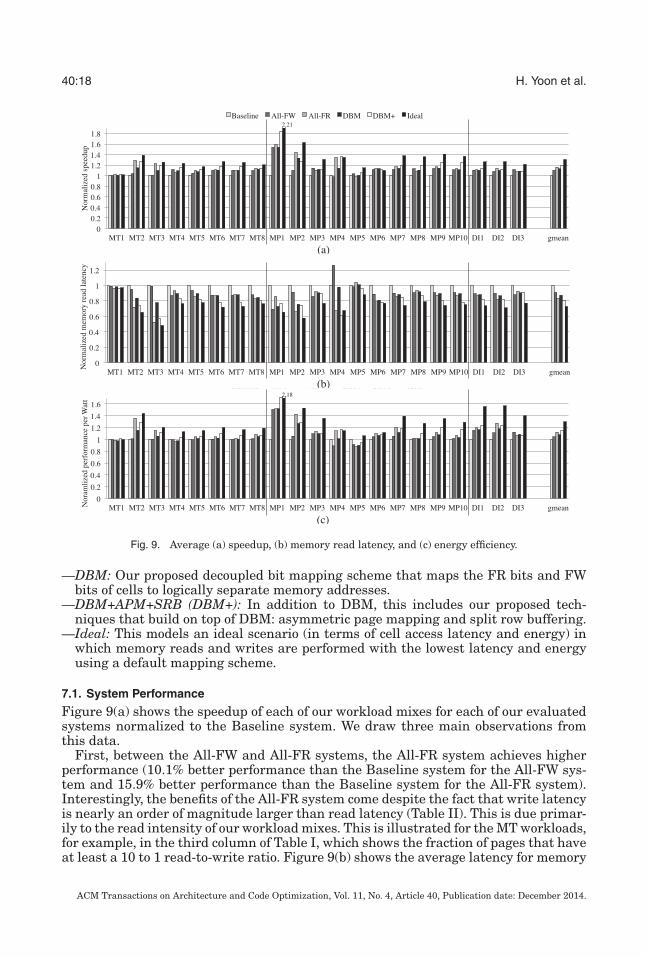
Fig. 9. Average (a) speedup, (b) memory read latency, and (c) energy efficiency.
—DBM: Our proposed decoupled bit mapping scheme that maps the FR bits and FWbits of cells to logically separate memory addresses.
—DBM+APM+SRB (DBM+): In addition to DBM, this includes our proposed tech-niques that build on top of DBM: asymmetric page mapping and split row buffering.
—Ideal: This models an ideal scenario (in terms of cell access latency and energy) inwhich memory reads and writes are performed with the lowest latency and energyusing a default mapping scheme.
7.1. System Performance
Figure 9(a) shows the speedup of each of our workload mixes for each of our evaluatedsystems normalized to the Baseline system. We draw three main observations fromthis data.
First, between the All-FW and All-FR systems, the All-FR system achieves higherperformance (10.1% better performance than the Baseline system for the All-FW sys-tem and 15.9% better performance than the Baseline system for the All-FR system).Interestingly, the benefits of the All-FR system come despite the fact that write latencyis nearly an order of magnitude larger than read latency (Table II). This is due primar-ily to the read intensity of our workload mixes. This is illustrated for the MT workloads,for example, in the third column of Table I, which shows the fraction of pages that haveat least a 10 to 1 read-to-write ratio. Figure 9(b) shows the average latency for memory
ACM Transactions on Architecture and Code Optimization, Vol. 11, No. 4, Article 40, Publication date: December 2014.

Efficient Data Mapping and Buffering Techniques for MLC PCM 40:19
Fig. 10. Various metrics comparing the different MLC PCM systems. Ratio of (a) read accesses to FR regionand (b) write accesses to FW region, showing that DBM+, by using APM, is able to make better use of themost efficient region for accessing data. (c) Row buffer hit ratio, showing that DBM+, by using SRB, is ableto use better row buffer management to improve row buffer hit ratio. (d) Normalized max slowdown, anunfairness metric, which shows that most techniques improve multicore fairness compared to the baseline.(e) shows how the improved memory throughput and higher average number of bits written with DBMand DBM+ affect memory lifetime and (f) illustrates how DBM and DBM+ trade off memory endurance foradditional performance.
read requests across the workloads for each of our evaluated systems. Notice that sys-tems with lower average memory read latency have higher performance, confirmingthat system performance for our workloads running on an MLC PCM main memory ishighly influenced by our workloads’ memory read intensity.
Second, using DBM alone achieves performance in between the All-FW and All-FRsystems (13.0% higher performance than the Baseline system). This is because DBMprovides both an FR region and an FW region, and the way an application’s data ismapped to each region depends on its virtual-to-physical address mapping, which inour experiments has been randomized to simulate the effects of OS mapping. Thus,some of each application’s data will be mapped into the FR region (with performancesimilar to the faster All-FR system) and some will be mapped into the FW region (withperformance similar to the slower All-FW system).
Third, the DBM+ system, which incorporates our APM and SRB techniques, is ableto achieve better performance than all the previously discussed systems (19.2% betterperformance than the Baseline system) by more intelligently managing how data isstored and retrieved from main memory. We can see that it effectively helps bridge thegap between a DBM-only system and an unachievable Ideal system, which has 30.5%better performance than the Baseline system.
To help understand the results in greater detail, Figure 10(a) shows what fraction ofread accesses are served in the FR region, and Figure 10(b) shows what fraction of writeaccesses are served in the FW region for the All-FW, All-FR, DBM, and DBM+ systems(note that for the Ideal system, the ratio would be 1.0 for both reads and writes). Wecan see that by employing APM, DBM+ is able to service a larger number of both readsand writes from the most efficient region of memory. In addition, Figure 10(c) showswhat fraction of accesses are serviced from the row buffer at lower latency and lowerenergy than accessing the MLC PCM array. We can see that by employing SRB, DBM+is able to achieve a higher row buffer hit ratio than the other techniques.
Some workloads do not follow these general patterns and are worth examining inmore detail. MP1, MP9, and MP10 all benefit the most from the better page placementdecisions of APM and additional amount of buffering provided by SRB in the DBM+technique as opposed to simply using DBM alone. Note that the Ideal system onlymodels ideal cell access latency and cell energy, not ideal data placement or databuffering, so that in some cases, such as MT1, MP4, and MP6 (which can performbetter data placement and buffering), the Ideal latency and energy system does notperform the best. For MP4, the All-FR technique performs worse than the baseline; in
ACM Transactions on Architecture and Code Optimization, Vol. 11, No. 4, Article 40, Publication date: December 2014.
40:20 H. Yoon et al.
MP5, the All-FW technique performs worse than the baseline because these workloadspredominantly write data (in the case of MP4) and read data (in the case of MP5).This can be seen by the large improvement in performance for MP4 when using theAll-FW technique and the improvement in performance for MP5 when using the All-FRtechnique (though the relative benefit for MP5 is less due to the lower latency of readscompared to writes). Finally, for workloads like MT4, MT7, MP3, MP5, MP8, and DI3,which perform many write accesses, the All-FW technique allows higher performancethan the All-FR technique. For workloads like these, our assumption in APM that datashould be allocated to the FR region by default can lead to lower performance thanwhen always allocating data to the FW region (as it does with MP3 and DI3). In thiscase, system designers can choose to tailor the default data placement decisions of APMto their workloads’ characteristics.
Overall, by employing our APM and SRB techniques on top of DBM, the DBM+system is able to improve performance by 19.2% compared to the Baseline system andgets within 11% of the Ideal system.
7.2. Memory Energy Efficiency
The energy efficiency of the memory system is shown in Figure 9(c) in terms of systemperformance per memory Watt (higher is better). Compared to the Baseline, the All-FWsystem achieves energy benefits only on write accesses, which, as we have discussed,are not the predominant access type in our workloads, leading to only a small benefitin terms of energy—4.4%. In contrast, the All-FR system improves energy efficiency by12.2% compared to the Baseline system.
While the DBM system has the potential to get the best of both the All-FW and All-FR systems in terms of energy efficiency, because it uses a default mapping of memoryand row buffer architecture, its energy efficiency lies in between the All-FW and All-FR systems, improving by only a modest 7.9% compared to the Baseline system. TheDBM+ system, on the other hand, is able to more efficiently utilize the FR and FWregions and more efficient row buffer organization provided by DBM, leading to anenergy efficiency improvement of 14.4% compared to the Baseline system. In this way,the DBM+ system helps achieves energy efficiency within 16% of the Ideal system.
7.3. System Fairness
Figure 10(d) shows the maximum slowdown (lower is better) of threads in the differentMLC PCM systems. The improved performance of DBM contributes to lowering themaximum slowdown by 12.7% relative to the Baseline system. The DBM+ system fur-ther enhances thread fairness with (1) higher performance and (2) the SRB technique,which reduces the contention among threads for use of the row buffer, lowering themaximum slowdown by 19.3% relative to the Baseline system. This is better than thefairness of the All-FW and All-FR systems (11.2% and 15.2% improvements, respec-tively, over the Baseline system), which also highlights the importance of optimizingfor both reads and writes in PCM systems, which ASM is able to help toward doing.
7.4. Memory Lifetime
Figure 10(e) shows the projected operational memory lifetime in years. We assume apessimistic cell endurance of 106 writes and a wear-leveling scheme that distributeswrites throughout 16GB of MLC PCM evenly. Two factors reduce the lifetimes of theDBM and DBM+ systems relative to the Baseline system. First, decoupled bit mappingdoubles the number of cells that are associated with a block, since a block occupies onebit (FR or FW) from each cell. Thus, to write to a block, more cells potentially need to beprogrammed (however, the probability of redundant bit-writes is lower in the Baselinesystem than in DBM [Zhou et al. 2009; Jiang et al. 2012b]). Second, DBM and DBM+
ACM Transactions on Architecture and Code Optimization, Vol. 11, No. 4, Article 40, Publication date: December 2014.

Efficient Data Mapping and Buffering Techniques for MLC PCM 40:21
Fig. 11. Performance sensitivity to different last-level cache sizes.
have higher system performance, which causes the two systems to issue writes at ahigher rate per unit time than the other systems, lowering memory lifetime.
To filter out the effect of system performance and isolate the effect of decoupledbit mapping on memory lifetime, we normalize the total number of cell-writes byperformance in Figure 10(f). The overhead for the DBM and DBM+ systems in termsof normalized cell writes/performance are 26.4% and 28.2%, respectively. We believe itis worthwhile to make this endurance tradeoff for performance, as recent work reportsthat much less pessimistic PCM endurance than we assumed for our study is possible(>109 writes) [Kim et al. 2010a]. The idea is that the asymmetric read/write propertiesin MLC PCM devices will continue to exist (due to the multilevel sensing requiredfor reads and the programming process required for writes), as PCM technology willimprove in terms of endurance.
7.5. Sensitivity to Last-Level Cache Size
Figure 11 shows the sensitivity of performance (instruction throughput) to differentlast-level cache sizes (plots are normalized to the Baseline system with an 8MB last-level cache size). The trends for throughput improvement are similar for the differentlast-level cache sizes (as are the trends for speedup). Relative to the Baseline system ineach individual category, DBM improves instruction throughput by 14.6%, 12.8%, and11.6% for the 8MB, 16MB, and 32MB last-level cache sizes, respectively. For DBM+,the improvements are 23.3%, 19.6%, and 18.3% for the same last-level cache sizes,outperforming the All-FR (18.6%, 16.1%, and 15.4%) and All-FW (10.7%, 9.6%, and7.7%) systems. The Ideal system improvements are 34.5%, 30.2%, and 30.3%. Withincreasing last-level cache size, the performance improvement relative to the baselinedecreases, as more requests for data are served by the last-level cache and less by thememory subsystem.
8. RELATED WORK
To our knowledge, this is the first work to (1) evaluate techniques to leverage MLCPCM’s asymmetric access characteristics in the context of a PCM main memory,(2) propose a hardware/software data mapping technique to leverage the asymmet-ric access characteristics of MLC PCM, and (3) propose a low-overhead row bufferorganization for MLC PCM that provides logically separate row buffers for each ofthe different bits in a multilevel cell. We next briefly discuss related research in othermemory technologies, in MLC PCM devices, and in leveraging multiple row buffers inmemory devices.
8.1. Related Concepts in Other Memory Technologies
The high-speed programming method in MLC Flash memory requires mapping thebits of an MLC cell to separate logical addresses. Although this resembles DBM, thetwo are fundamentally different. High-speed programming in Flash is designed to
ACM Transactions on Architecture and Code Optimization, Vol. 11, No. 4, Article 40, Publication date: December 2014.
40:22 H. Yoon et al.
reduce the number of intermediate read verifications between successive programmingiterations [Takeuchi et al. 1998]. On the other hand, DBM is motivated by MLC PCM’sread and write asymmetry properties, which are exploited to expose the lower latencyand energy of FR region reads and FW region writes. Jiang et al. [2012a] proposemapping the bits of an MLC STT-RAM cell to separate logical addresses to increasethe performance of on-chip caches in embedded processors. Their mechanism migratesdata to favorable memory locations depending on the observed type of accesses (readsor writes) frequently issued to the data. This is different from APM, which predictswhether data is read- or write-intensive before allocating it to memory locations, andour technique could potentially be used in STT-RAM caches. Recent work examiningMLC resistive RAM [Niu et al. 2013] has looked at different ways of mapping data tocells to eliminate certain high-latency and high-energy states. These techniques couldpotentially be applied, in conjunction with our techniques, in MLC PCM cells thatcontain more than two levels (at only two levels, these techniques cannot leverage thecapacity benefits of MLC).
8.2. Multilevel Cell PCM
Qureshi et al. [2010b] proposed dynamically adapting the usage of PCM either ashigh-density, high-latency MLC memory or as low-density, low-latency SLC memory,depending on the memory requirements of the application. Their work assumes thata system has overprovisioned memory capacity, and trades away surplus capacity forreduced latency. Our proposal reduces the latency while maintaining the high densityof MLC PCM, through data mapping that exploits lower-bit latency and enables fine-granularity row buffering. This does not prevent the memory from being configured asMLC or SLC, and is thus orthogonal work.
Other works have introduced ways to mitigate the high write latency of MLC PCM.Write cancellation and pausing allow reads to be served faster by interrupting longwrite operations [Qureshi et al. 2010a]. Jiang et al. [2012b] proposed write truncationthat improves write latency by foregoing the programming of the few slower bits in arow (or block), compensating for the loss in data integrity with stronger ECC. They alsoproposed to store data in SLC form if the data and associated ECC bits can altogetherbe compressed to less than half of the original data size. These studies and others [Leeet al. 2010a; Yoon et al. 2012; Meza et al. 2012a] primarily focus on alleviating the highMLC PCM write latency (with read enhancements depending on the compressibility ofthe data). Both can be applied in conjunction with our proposals.
The practicality of MLC PCM technology has been demonstrated by various works[Bedeschi et al. 2009; Close et al. 2011; Papandreou et al. 2011]. Architectural solutionshave been proposed to prolong memory lifetime through wear-leveling [Zhou et al. 2009;Qureshi et al. 2009a; Cho and Lee 2009], enhancing fault-tolerance [Ipek et al. 2010;Schechter et al. 2010; Yoon et al. 2011], data buffering [Qureshi et al. 2009b; Lee et al.2009], and programming-current provisioning [Zhang et al. 2009]. These schemes aregeneric to SLC and MLC PCM, and can also be used in addition to our proposals.
8.3. Multiple Row Buffers
Several prior studies [Hsu and Smith 1993; Zhang et al. 2001; Loh 2008; Lee et al. 2009]evaluated the use of multiple row buffers in memory devices, showing that it generallyleads to increased row buffer locality and memory performance gains. However, whenresizing the length of each row buffer (e.g., for the purpose of reducing or maintainingthe die area occupied by row buffers), Hsu and Smith [1993], Zhang et al. [2001],Lee et al. [2009], and Meza et al. [2012a] show that it harms performance if the rowbuffers are too short. This is because shorter row buffers exploit less spatial locality.In other words, for a constant die area dedicated to row buffers, there is a point at
ACM Transactions on Architecture and Code Optimization, Vol. 11, No. 4, Article 40, Publication date: December 2014.

Efficient Data Mapping and Buffering Techniques for MLC PCM 40:23
which increasing the number of row buffers at the expense of having them shorter isno longer desirable.
We propose a fine-granularity row buffer organization that divides the row bufferbetween the bits of an MLC cell (i.e., between the FR bits and the FW bits), insteadof dividing the row buffer between the bitlines in a row. For DBM, where the bitsof a cell are mapped to logically separate memory addresses, our scheme enables afine-granularity row buffer organization while not diminishing spatial locality.
9. CONCLUSION
We presented new data mapping and buffering techniques that enable higher per-formance and energy efficiency by exploiting characteristics of multilevel cell phase-change memory technology. Our proposed approaches are built on decoupled bit map-ping, which leverages the asymmetric read/write characteristics of MLC PCM cells.We examined two techniques enabled by decoupled bit mapping. Our first techniqueuses a hardware/software cooperative policy to map data in MLC PCM in a way thatexploits the asymmetric read/write characteristics between the bits of an MLC PCMcell. The system software receives predictions from the hardware about the read/writeaffinity of data, then maps read-intensive pages to a fast-read/slow-write (FR) regionand write-intensive pages to a slow-read/fast-write (FW) region. Our second techniqueexploits the flexibility in row buffering enabled by decoupled bit mapping to providetwo logical row buffers from a single physical row buffer. This increases row bufferlocality, enhancing both memory performance and energy efficiency. Our evaluationsfor a multicore system show that the proposed techniques provide better system perfor-mance, energy efficiency, and thread fairness compared to the conventional MLC PCMbaseline. We believe that our proposals provide an effective way of taking advantageof MLC technology in main memory in a way that is also applicable to other emergingtechnologies with similar characteristics.
ACKNOWLEDGMENTS
We thank the anonymous reviewers and the members of the SAFARI research group for their commentsand suggestions. This work is supported in part by NSF grants 0953246, 1212962, 1320531, the IntelScience and Technology Center for Cloud Computing, and the Semiconductor Research Corporation. Wegratefully acknowledge the support of our industrial partners, including Hewlett-Packard Labs, IBM, Intel,Qualcomm, and VMware. Part of this work was done while HanBin Yoon and Justin Meza were interns atHewlett-Packard Labs.
REFERENCES
L. A. Barroso and others. 2013. The Datacenter as a Computer. Morgan & Claypool, San Francisco, CA.F. Bedeschi and others. 2009. A Bipolar-Selected Phase Change Memory Featuring Multi-Level Cell Storage.
JSSC (2009).M. Bender and others. 1998. Flow and Stretch Metrics for Scheduling Continuous Job Streams. In SODA.B. Buros. 2012. Tuning and Optimizing malloc on PowerLinux. IBM developerWorks (PowerLinux Ar-
chitecture) (2012). Retrieved October 26, 2014 from http://www.ibm.com/developerworks/wikis/display/LinuxP/Tuning+and+optimizing+malloc+on+PowerLinux.
Y. Cai and others. 2012. Error Patterns in MLC NAND Flash Memory: Measurement, Characterization, andAnalysis. In DATE.
Y. Cai and others. 2013. Threshold Voltage Distribution in MLC NAND Flash Memory: Characterization,Analysis, and Modeling. In DATE.
S. Cho and H. Lee. 2009. Flip-N-Write: A Simple Deterministic Technique to Improve PRAM Write Perfor-mance, Energy and Endurance. In MICRO.
G. F. Close and others. 2011. A 512Mb Phase-Change Memory (PCM) in 90nm CMOS Achieving 2b/cell. InVLSIC.
R. Das and others. 2009. Application-Aware Prioritization Mechanisms for On-Chip Networks. In MICRO.
ACM Transactions on Architecture and Code Optimization, Vol. 11, No. 4, Article 40, Publication date: December 2014.
40:24 H. Yoon et al.
G. Dhiman and others. 2009. PDRAM: a Hybrid PRAM and DRAM Main Memory System. In DAC.W. Doerner. 2012. Memory Allocation and First-Touch. Intel Developer Zone (2012). http://software.intel.com/
en-us/articles/memory-allocation-and-first-touch.X. Dong and others. 2012. NVSim: A Circuit-Level Performance, Energy, and Area Model for Emerging
Nonvolatile Memory. TCAD (2012).T. D. Happ and others. 2006. Novel One-Mask Self-Heating Pillar Phase Change Memory. In VLSIT.M. Hosomi and others. 2005. A Novel Non-Volatile Memory with Spin Torque Transfer Magnetization
Switching: Spin-RAM. In IEDM.W.-C. Hsu and J. E. Smith. 1993. Performance of Cached DRAM Organizations in Vector Supercomputers.
In ISCA.E. Ipek and others. 2010. Dynamically Replicated Memory: Building Reliable Systems from Nanoscale
Resistive Memories. In ASPLOS.L. Jiang and others. 2012a. Constructing Large and Fast Multi-Level Cell STT-MRAM Based Cache for
Embedded Processors. In DAC.L. Jiang and others. 2012b. Improving Write Operations in MLC Phase Change Memory. In HPCA.M. Joshi and others. 2011. Mercury: A Fast and Energy-Efficient Multi-Level Cell Based Phase Change
Memory System. In HPCA.R. Kalla and others. 2010. Power7: IBM’s Next-Generation Server Processor. Micro, IEEE (2010).P. Kaminski. 2009. NUMA Aware Heap Memory Manager. AMD Developer Central (2009). http://developer.
amd.com/wordpress/media/2012/10/NUMA_aware_heap_memory_manager_article_final.pdf.S. Kang and others. 2007. A 0.1-um 1.8-V 256-Mb Phase-Change Random Access Memory (PRAM) with
66-MHz Synchronous Burst-Read Operation. JSSC (2007).I. S. Kim and others. 2010a. High Performance PRAM Cell Scalable to Sub-20nm Technology with below 4F2
Cell Size, Extendable to DRAM Applications. In VLSIT.Y. Kim and others. 2010b. ATLAS: A Scalable and High-Performance Scheduling Algorithm for Multiple
Memory Controllers. In HPCA.Y. Kim and others. 2010c. Thread Cluster Memory Scheduling: Exploiting Differences in Memory Access
Behavior. In MICRO.H. Kwak and others. 2010. What is Twitter, a Social Network or a News Media? Retreived October 25, 2014
from http://an.kaist.ac.kr/traces/WWW2010.html. In WWW.B. C. Lee and others. 2009. Architecting Phase Change Memory as a Scalable DRAM Alternative. In ISCA.B. C. Lee and others. 2010a. Phase Change Memory and the Quest for Scalability. In CACM.B. C. Lee and others. 2010b. Phase-Change Technology and the Future of Main Memory. In IEEE Micro.G. H. Loh. 2008. 3D-Stacked Memory Architectures for Multi-core Processors. In ISCA.J. Meza and others. 2012a. A Case for Small Row Buffers in Non-Volatile Main Memories. In ICCD.J. Meza and others. 2012b. Enabling Efficient and Scalable Hybrid Memories Using Fine-Granularity DRAM
Cache Management. CAL.T. Nirschl and others. 2007. Write Strategies for 2 and 4-bit Multi-Level Phase-Change Memory. In IEDM.D. Niu and others. 2013. Low Power Multi-Level-Cell Resistive Memory Design with Incomplete Data
Mapping (ICCD).N. Papandreou and others. 2011. Drift-Tolerant Multilevel Phase-Change Memory. In Intl. Memory Workshop
(IMW).H. Patil and others. 2004. Pinpointing Representative Portions of Large Intel Itanium Programs with Dy-
namic Instrumentation. In MICRO.M. K. Qureshi and others. 2009a. Enhancing Lifetime and Security of PCM-Based Main Memory with
Start-Gap Wear Leveling. In MICRO.M. K. Qureshi and others. 2009b. Scalable High Performance Main Memory System Using Phase-Change
Memory Technology. In ISCA.M. K. Qureshi and others. 2010a. Improving Read Performance of Phase Change Memories via Write Can-
cellation and Write Pausing. In HPCA.M. K. Qureshi and others. 2010b. Morphable Memory System: a Robust Architecture for Exploiting Multi-
Level Phase Change Memories. In ISCA.M. K. Qureshi and others. 2012. PreSET: Improving Performance of Phase Change Memories by Exploiting
Asymmetry in Write Times. In ISCA.L. Ramos and others. 2011. Page Placement in Hybrid Memory Systems. In ICS.S. Raoux and others. 2008. Phase-Change Random Access Memory: A Scalable Technology. IBM J. Res. Dev.
ACM Transactions on Architecture and Code Optimization, Vol. 11, No. 4, Article 40, Publication date: December 2014.

Efficient Data Mapping and Buffering Techniques for MLC PCM 40:25
S. Rixner and others. 2000. Memory Access Scheduling. In ISCA.S. Schechter and others. 2010. Use ECP, Not ECC, for Hard Failures in Resistive Memories. In ISCA.N. H. Seong and others. 2013. Tri-Level-Cell Phase Change Memory: Toward an Efficient and Reliable
Memory System. In ISCA.A. Snavely and D. M. Tullsen. 2000. Symbiotic Jobscheduling for a Simultaneous Multithreading Processor.
In ASPLOS.D. B. Strukov and others. 2008. The Missing Memristor Found. Nature.K.-D. Suh and others. 1995. A 3.3 V 32 Mb NAND Flash Memory with Incremental Step Pulse Programming
Scheme. In JSSC.K. Takeuchi and others. 1998. A Multipage Cell Architecture for High-Speed Programming Multilevel NAND
Flash Memories. JSSC (1998).The International Technology Roadmap for Semiconductors. 2010. Process Integration, Devices, and
Structures.H. Vandierendonck and A. Seznec. 2011. Fairness Metrics for Multi-Threaded Processors. In CAL.H. P. Wong and others. 2010. Phase Change Memory. In Proc. of the IEEE (2010).D. H. Yoon and others. 2011. FREE-p: Protecting Non-Volatile Memory Against Both Hard and Soft Errors.
In HPCA.H. Yoon and others. 2012. Row Buffer Locality Aware Caching Policies for Hybrid Memories. In ICCD.H. Yoon and others. 2013. Techniques for Data Mapping and Buffering to Exploit Asymmetry in Multi-Level
Cell (Phase Change) Memory. Technical Report. Carnegie Mellon University, Pittsburgh, PA.W. Zhang and others. 2009. Characterizing and Mitigating the Impact of Process Variations on Phase Change
Based Memory Systems. In MICRO.Z. Zhang and others. 2001. Cached DRAM for ILP Processor Memory Access Latency Reduction. In Micro,
IEEE (2001).P. Zhou and others. 2009. A Durable and Energy Efficient Main Memory Using Phase Change Memory
Technology. In ISCA.W. K. Zuravleff and T. Robinson. 1997. Controller for a Synchronous DRAM That Maximizes Throughput by
Allowing Memory Requests and Commands to be Issued Out of Order. In U.S. Patent Number 5,630,096,Filed May 10, 1995, Issued May 13, 1997.
Received March 2014; revised June 2014; accepted September 2014
ACM Transactions on Architecture and Code Optimization, Vol. 11, No. 4, Article 40, Publication date: December 2014.