eindhoven university of technology master an all-active 2r … · eindhoven university oftechnology...
TRANSCRIPT

Eindhoven University of Technology
MASTER
An all-active 2R regenerator using POLIS
Marell, M.J.H.
Award date:2006
Link to publication
DisclaimerThis document contains a student thesis (bachelor's or master's), as authored by a student at Eindhoven University of Technology. Studenttheses are made available in the TU/e repository upon obtaining the required degree. The grade received is not published on the documentas presented in the repository. The required complexity or quality of research of student theses may vary by program, and the requiredminimum study period may vary in duration.
General rightsCopyright and moral rights for the publications made accessible in the public portal are retained by the authors and/or other copyright ownersand it is a condition of accessing publications that users recognise and abide by the legal requirements associated with these rights.
• Users may download and print one copy of any publication from the public portal for the purpose of private study or research. • You may not further distribute the material or use it for any profit-making activity or commercial gain

--I.U1e !e(hnis(he "nivers;!e;! eindhoven
An all-active 2R regeneratorusing POLIS
By M.J.H. Marell
jfaculteit elektrotechniek

Eindhoven University of TechnologyFaculty of Electrical EngineeringDivision of Telecommunication Technology and ElectromagneticsOpto-Electronics Devices Group
TTE-OED
AN ALL-ACTIVE 2R REGENERATOR
USING POLIS
by M.l.H. Marell
Master of Science Thesiscarried out from 01/09/2005 to 17/0812006
Supervisors:Dr. J.l.G.M. van der TolDr. E.AJ.M. Bente
Graduation professor:Prof. Dr. Ir. M.K. Smit
The Faculty of Electrical Engineering of Eindhoven University ofTechnology disclaims allresponsibility for the contents of traineeship and graduation reports.

Graduation Thesis
An all-active 2R regenerator using POLIS
NameStudent numberDateInstitute
Supervisors TU/e
Graduation professor
M.J.R. Marell049165117th August 2006Eindhoven University of Technology (TU/e)Faculty of Electrical and Electronic EngineeringTelecommunication Technology and Electromagnetics (TTE)Opto-Electronic Devices (OED)
Dr. J.J.M.G. van der TolDr. E.A.J .M. BenteProf. Dr. Ir. M.K. Smit
COBRA Research Institute, Technische Universiteit Eindhoven,
Postbus 513, 5600 MB Eindhoven, The Netherlands
August 30, 2006

2
"Ni bhionn an duine crionna go dteann an beart thart"Irish saying

CONTENTS
Contents 3
List of constants and symbols 7
1 Introduction 9
1.1 Optical communication. 9
1.2 Semiconductor materials . 10
1.3 Multiple layers ..... 12
Double hetero junction. 12
Quantum well . . . . . . 13
Strain in quantum wells 14
1.4 Optical integration . 16
The POLIS concept 16
2 The concept 19
2.1 Introduction. 19
2.2 2R Regeneration 21
2.3 Principle of operation 22
2.4 Static Analysis 24
2.5 Mode-locking 26
3 Device modeling 29
3.1 Introduction. ....... 29
3.2 The traveling wave model 30
3.3 Basic operation of the software 32
3.4 Design considerations 32
Gain suppression ... 32
Linewidth enhancement factor. 33
3

4
Polarization mode dispersion ....
Polarization dependent amplification
The Kerr effect . . . . . . . . . . .
3.5 Modifications to the original model
3.6 Semiconductor Optical Amplifiers.
Introduction. . . . . . . .
Mathematical description
3.7 Waveguides . . . . . .
4 Polarization converters
4.1 Introduction .
4.2 Polarization conversion.
4.3 Mathematical description
4.4 The ideal polarization converter .
4.5 Polarization converters with losses
4.6 Polarization converters with a phase mismatch
4.7 Power dependence of quantum well polarization mode converters
Measurement setup .
Measurement results
5 Device characterization
5.1 Introduction.
5.2 Parameters
5.3 Simulations
SOA length and gain
Partial polarization converters.
Full polarization converter . . .
Losses in the polarization converters
Phase mismatch in the polarization converters.
5.4 Dynamic behavior .
SOA length and gain
Partial polarization converters.
Full polarization converters . .
Losses in the polarization converters
Phase mismatch in the polarization converters.
Contents
34
35
35
36
36
36
37
39
41
41
41
42
45
45
46
47
49
51
57
57
57
58
59
62
63
64
65
66
67
68
70
71
72

Contents
Pulse narrowing .
Reshaping ....
Noise suppression.
Regeneration of multiple pulses
Mode-locking . . . . . . . . . .
6 Conclusions and recommendations
6.1 Conclusions
Simulations
Measurements .
6.2 Recommendations
Bibliography
Appendices
A Polarization of light
B Self phase modulation
C 2R Regeneration
D Dynamic operation of the device
E Variable step size integration
F MATLAB model polarization converters
G MATLAB model Self Phase Modulation
5
73
73
74
74
76
79
79
79
80
81
83
85
87
89
93
95
97
99
101

LIST OF CONSTANTS AND SYMBOLS
c speed of light 2.99792 . 108 m/se elementary charge 1.60219. 10-19 CEO permittivity in vacuum 8.85419. 10-12 F/m C2/J·mh Planck's constant 6.62618 . 10-34 Jsh h/27r 1.05459 . 10-34 Jsk Boltzmann's constant 1.38066 . 10-23 J/K{La permeability in vacuum 47r·1O- 7 H/m
TABLE 1: Constants
aaN
aT
aint
13mrrKerr
fJ
vWm
a
TS
TSHB
</J
</J</J(x,y)<I>(z)'ljJ'1/;
linewidth enhancement factorcarrier linewidth enhancement factortemperature linewidth enhancement factorinternal absorptionpropagation constantconfinement factorkerr confinement factorphase mismatchgain suppression constantgain suppression due to spectral hole burningcoupling constantwavelengthfrequency of the lightradial frequency of the lighteffective areaspontaneous recombination timerecovery time spectral hole burninglinear phase shift obtained in an SOAphase of the TE polarizationspatial distribution of the optical fieldenvelope of the electron wave functiontotal phase shift obtained in an SOAphase of the TM polarization
7

8
aNAA±
mA act
BCdz
EEEgap
Ephoton
ExEy
9g(N, E)g(N, E,S)gogEIkLBm
ne
n x
n y
NNE
NEOPSSEvg
V(f}Vact
Vqw(z)X and x
o. List of constants and symbols
gain cross-sectionspontaneous recombination rateslowly varying envelopesurface active regionbimolecular recombination rateauger recombination ratethickness of the quantum wellenergyelectric fieldband-gap energyphoton energyelectric field x-componentelectric field y-componentgaingain as a function of carrier density and photon energygain as a function of carrier density, photon energy and photon densitysmall signal gaingain at energy Einjection currentphoton momentumbeat lengthsub-band numbereffective particle massrefractive indexnon-linear refractive indexeffective refractive indexrefractive index in x-directionrefractive index in y-directioncarrier densitycarrier density available for energy Ecarrier density available for energy E in steady stateoptical powerphoton densityphoton density with energy Egroup velocityperiodic lattice potential (3-D)volume active regionquantum well potential (I-D)conversion factor
TABLE 2: Symbols

1INTRODUCTION
1.1. OPTICAL COMMUNICATION
Communication is one of the principal needs of people. Their urge to communicate hasbeen the driving force for the study and development of all sorts of communication systems,capable of exchanging information between two or more places. During the ages of history,people have continuously increased their demands on the capabilities of these communicationsystems. The distance over which information was exchanged increased dramatically and sodid the amount and value of the information. This imposed constraints on the speed and thereliability of the systems.
In the very beginning, the rate of information exchange was very low. Only simple opticaland acoustical means, such as lamps, horns or smoke, were involved in the process. A new,more sophisticated way of communicating started with the invention of the telegraph. It wasthe first step towards electrical communication. The main trend in electrical communicationwas to superimpose information on sinusoidally varying electro-magnetic waves, the so-calledcarrier waves. At the point of reception the information is removed from the carrier wave andthen further processed to make the information available for the end user. This has severaladvantages: carrier waves with different frequencies can be distinguished from each other andthe channel capacity increases with increasing carrier frequency. Systems involved in electricalcommunication would therefore use an ever increasing part of the electro-magnetic spectrum.
Approximately 25 years a go, two major breakthroughs were achieved in communicationsystems. They involved the invention of the semiconductor laser and the low-loss opticalfiber at nearly the same time. With these invention, a, till that time unexplored part of theelectro-magnetic spectrum, could now be exploited. Since that time, communication systemshave gone through an explosive development.
Optical signals can be guided in similar ways as signals from the radio-frequency part ofthe spectrum, through free space or guided by a channel. In contrast to electrical communication, however, the intensity of the optical power, rather than the frequency of the carrier ismodulated. The bandwidth of optical signals is expressed in units of wavelength, instead offrequency. The wavelength of the light used in optical communication systems varies between800 nm and 1600 nm, which corresponds to a band-width of approximately 190 THz. The
9

10 Chapter 1. Introduction
reason why this particular wavelength region is used, is that the optical fibers exert the lowest losses on signals in this wavelength range. This enormous bandwidth is one of the mainadvantages of optical communication systems, together with the high speed of light in theguiding media.
A recent achievement in optical communication systems demonstrates the possibility ofcreating an error-free link with the capacity of 22 times 21.4 Gbps over a distance of 10.500km [1]. How big an amount of data this is, is nearly impossible to grasp. Expressed in termsof 64 Kbps phone calls, this corresponds to the transmission of 7.5 million calls over a singlefibre at the same time.
The increasing amount of data and the simultaneously increasing distance over whichthe data is transported bring along difficulties. No matter how low-loss the fibers used inthe system and no matter how big the output power of the lasers might be, optical signalsalways degrade due to imperfections in the various components. Clever tricks and modulationschemes can be used in order to be able to transfer the data from one point to another evenover a 'bad' communication system. However, there's always a limit to the amount of errorsthat can be corrected or to the speed with which the data is sent. Therefore other opticalcomponents were developed to improve or manipulate the signals along their way.
There's an endless list of examples of such devices (e.g. splitters. couplers, amplifiers,regenerators, switches etc.). They all have in common that there is an increasing demand formonolithically integrated versions of the functions they represent. The reason for this is thatmore and more of these devices are needed and that space becomes a limiting factor. Thecontemporary knowledge of semiconductor materials and their processing offers the possibilityto manipulate these materials in the most bizar ways and so creates a great flexibility forimplementing devices with a great variety of functions on a very small scale.
In this thesis, the feasibility of integrating an all optical regenerator is discussed. Thepurpose of such a device is restoring the integrity of an optical signal. The concept of theregenerator is new in itself, as well as the integration scheme on which the concept of theregenerator is based. Integrating new optical functionality is never without problems. Evenmore issues are involved if these new device concepts require require new material schemes.These problems concern the operation of the device and the fabrication. A careful studythus has to be performed in advance. This thesis studies the dynamic behavior of the deviceconcept of the regenerator and reports on the results gained in this study.
1.2. SEMICONDUCTOR MATERIALS
Semiconductors thank their name to the fact that their conduction properties lie somewherebetween those of conductors (such as metals) and insulators. The properties of these materialscan be interpreted with the help of energy band-diagrams (see figure 1.1). In order to find outwhat a band diagram exactly is, let us consider the material Silicon as an example. Siliconis located in the fourth column in the periodic table of elements. One atom of the materialhas four electrons in its outer shell, by which they can make covalent bonds with neighboringatoms in the crystal lattice.
A simple energy band-diagram consists of two energy bands, the so-called conductionband and the valence band. Both bands are separated by the band-gap, in which no other

1.2. Semiconductor materials
Donor _ ED
Acceptor ...... E.E,
Transverse direction
FIGURE 1.1: A simple band diagram as function of the transverse position
11
energy levels exist. In a pure crystal at very low temperatures, all electrons in the outer shellof the atom are bonded to the atom core. In this situation the conduction band is completelyempty and the valence band is completely filled. By adding energy to the system, the energyof the electrons is increased. If the energy is increased above the band-gap, the bond betweenthe electrons and the core is broken. This leads to a number of electrons in the conductionband and a number of "holes" in the valence band.
The conductivity of semiconductors can be greatly improved by adding so-called impurities to the material. These impurities can be atoms from the third or fifth column of theperiodic table of elements. The outer shell of atoms from these columns contain three or fiveelectrons respectively. If. for example. one atom from the fifth column is added in a crystalcontaining only Silicon atoms, four of the electrons of the impurity atom bond with the fourelectrons of the neighboring Silicon atoms and the fifth electron becomes a loosely boundelectron that is available for conduction after overcoming a significantly smaller amount ofenergy than the original band-gap. This process is called doping and can be done to addadditional holes as well. Doped materials are referred to as extrinsic materials.
Ec • 0 •1.- .-l .-1::
Ev0 • 0
Sp. Emission Absorption St. Emission
FIGURE 1.2: Generation and annihilation of electron-hole pairs
There are several ways in which carriers can be moved from the valence band to theconduction band and the other way around. The most important are shown in figure 1.2. Anelectron transition can take place under the emission or absorption of a photon. In this caseboth energy and momentum have to be conserved, because of the particle nature of light.Photons can contain a considerable amount of energy, their momentum (k), however, is verysmall, because of their negligible mass. Semiconductor materials can be classified as eitherhaving a direct band-gap or an indirect band-gap, depending on the shape of the band-gap asa function of the momentum. In the simplest and most probable recombination process, the

12 Chapter 1. Introduction
electron and hole involved have the same momentum. The material is then called a directband-gap material. In indirect band-gap materials lattice vibrations, called phonons, areinvolved to conserve momentum.
Conduction band
~c:w
Second valley
E.. Direct Indirect
Valence band
FIGURE 1.3: Direct (red) and indirect (blue) bandgap transitions as a function of k
Semiconductor materials used in the active layers of lasers and amplifiers need to have adirect band-gap (see figure 1.3). Only in this kind of material is the radiative recombinationprocess sufficiently strong to reach an adequate level of optical emission. Unfortunatelyno single-element semiconductor has a direct band-gap. Binary, ternary and quarternarycompounds of semiconductors, however, can have a direct band-gap and are therefore suitablefor the use in optical active elements. The most important elements are the ones from thethird and fifth column of the periodic table of elements, better known as the III-V materials.Examples of III-V materials are Indium, Gallium, Arsenide and Phosphide.
To achieve emission at longer wavelengths, around 1500 nm, the quarternary alloyInl-xGo,xAsyPl-y is the most suitable. By varying the mole fractions of the elements inthe compound an interesting property of the material becomes clear. Varying the variousfractions the wavelength corresponding to the band-gap of the material can be chosen freely,anywhere between 1.0 pm and 1.7 11m. Beside the choice in emission wavelength, also thelattice constant of the material can be varied by changing the mole fractions. In this way thelattice constants of two adjoining semiconductor materials can be matched quite accurately inorder to prevent defects and in order to add or remove stress at the interface of the materials.All these parameters have an influence on the radiative recombination process in opticaldevices.
1.3. MULTIPLE LAYERS
DOUBLE HETERO JUNCTION
By sandwiching a layer of, for example, quarternary material between two other layers witha larger band-gap (as shown in figure 1.4(a)), a so-called potential well is created for theelectrons and holes. A potential well is a region surrounding a local minimum of potentialenergy, in this case formed by the surrounding layers with the larger band-gap. Energy

1.3. Multiple layers 13
captured in the potential well is unable to convert to another type of energy because it iscaptured at the local minimum of the potential well. The potential well confines free carriersto the layer with the smallest band-gap. This way recombination of electrons and holes canbe forced to take place in this specific layer, which generates photons with an energy equalto Ephotcm = E gap = hv. In this equation Ephotcm represents the photon energy, h and vrepresent Planck's constant and the optical frequency of the light respectively.
Conduction band
2 3
Conduction band
5
UJ•UJ
Valence band
(a)
Valence band
(b)
FIGURE 1.4: A double hetero junction (a) and a quantum well (b)
QUANTUM WELL
If the dimensions of a semiconductor potential well are, decreased so that the thickness ofthe layer approximates the DeBroglie wavelength of the carriers (about 10 nm for semiconductor materials), quantum effects become apparent. Because of the small dimensions, thefree electron motion is limited from 3 dimensions to 2 dimensions. This kind of quantumconfinement is called a quantum well (see figure 1.4(b)). The spatial limitations not onlyhave a drastic effect on the confinement of the electrons and holes, but on other propertiesof the semiconductor material as well. Quantum wells, are, for example, known to enhancethe material gain, improve response times and lower the transparency carrier density of thematerial.
(1.1 )
In general, the electron wave function needs to satisfy the Schrodinger equation, in whichthe potential V(f') represents the periodic semiconductor crystal. For a quantum well, anadditional potential Vqw(z) has to be added to the periodic potential V(f'). The quasi twodimensional nature causes the conduction and valence band to be split in energy subbands,i.e. the carriers can only have discrete energy levels. These discrete energy levels correspondto discrete wavenumbers, rather than the continuous conduction and valence bands in bulkmaterial. These energy levels can be found by solving <l>(z), the envelope function, from the

14 Chapter 1. Introduction
one dimensional Schrodinger equation given by equation 1.1. In this equation the periodiccrystal potential V(f') is represented by the effective mass m~, which is different for well andbarrier materials, Ii is the reduced Planck constant. The solutions, for a deep quantum well,lead to the following energy levels:
corresponding to discrete wave numbers. In equation 1.2 msubband and dz is the thickness of the quantum well layer.
STRAIN IN QUANTUM WELLS
(1.2)
1, 2, 3 . .. indicates the
Application of strain in quantum well layers is a widely used technique in the field of optoelectronics to improve the optical properties of quantum well material even further. Thestrain is generated by varying the material composition so that the lattice constant is slightlydifferent from the that of the neighboring layers, known as the barrier layers or the SeparateConfinement Hetrostructure layers (SCH).
One can distinguish two types of strain: tensile strain and compressive strain. By choosingthe lattice constant of the barrier layers to be bigger than the lattice constant of the well,causes the well to be stretched by the barrier layers. By giving the barrier layers a latticeconstant smaller than the constant of the well, one can compress the well.
(a) (b)
FIGURE 1.5: Compressive strain (8) and a tensile strain (b)
The reason why one can successfully apply strain to a layer of semiconductor material isthe thin nature of this layer. The thickness of a quantum well layer is usually limited to afew nanometers and, for the application of strain, it must be smaller than a critical thicknessto prevent lattice relaxation.
In order to fully understand the result of the application of strain in a quantum well, wehave to extend our view of the composition of the energy bands in semiconductor material(figure 1.3). The electron states at the bottom of the conduction band have zero orbitalangular momentum (s-like) and are isotropic in space. The hole states at the top of thevalence band have a none-zero angular momentum (p-like) and are anisotropic in space. Onecan distinguish three different states. corresponding to three valence bands. The heavy-holeband, the ligh-hole band and the split-off band. For quarternary material. the heavy-hole andthe light-hole band usually overlap at the r point, at which k z = O.
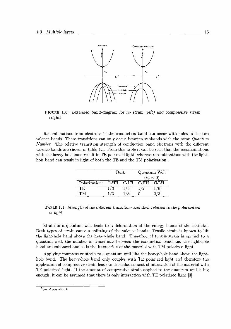
1.3. Multiple layers
No strain Compressive strain
15
FIGURE 1.6: Extended band-diagram for no strain (left) and compressive strain(right)
Recombinations from electrons in the conduction band can occur with holes in the twovalence bands. These transitions can only occur between subbands with the same QuantumNumber. The relative transition strength of conduction band electrons with the differentvalence bands are shown in table 1.1. From this table it can be seen that the recombinationswith the heavy-hole band result in TE polarized light, whereas recombinations with the lighthole band can result in light of both the TE and the TM polarization1.
Bulk
Polarization:TETM
C-HH1/31/3
C-LH1/31/3
Quantum Well(kz rv 0)
C-HH C-LH1/2 1/6o 2/3
TABLE 1.1: Strength of tile different transitions and their relation to the polarizationof light
Strain in a quantum well leads to a deformation of the energy bands of the material.Both types of strain cause a splitting of the valence bands. Tensile strain is known to liftthe light-hole band above the heavy-hole band. Therefore, if tensile strain is applied to aquantum well, the number of transitions between the conduction band and the light-holeband are enhanced and so is the interaction of the material with TM polarized light.
Applying compressive strain to a quantum well lifts the heavy-hole band above the lighthole band. The heavy-hole band only couples with TE polarized light and therefore theapplication of compressive strain leads to the enhancement of interaction of the material withTE polarized light. If the amount of compressive strain applied to the quantum well is bigenough, it can be assumed that there is only interaction with TE polarized light [3].
ISee Appendix A
16 Chapter 1. Introduction
104. OPTICAL INTEGRATION
After a short introduction on the active behavior of semiconductor materials a closer look canbe taken at the integration of optical devices. Integrated optical devices consist of many layersof different semiconductor materials of which the crystal structure must be carefully takeninto account. In any crystal, atoms or groups of atoms are arranged in repeated patterns inspace. Such a periodic arrangement defines a so-called lattice and the spacing between the(groups of) atoms is called the lattice constant. A stack of unprocessed layers of crystallinesemiconductor material is called a wafer. The fabrication of a layer stack is started from acrystalline substrate, which provides the devices on the wafer with enough strength to bemounted after the processing and which can be used as an electrical contact.
A technique of crystal growth by chemical reaction is used to grow thin layers of semiconductor material on the substrate. All these layers must have lattice structures comparableto that of the substrate, i.e. the layers are lattice-matched (in the case of no strain). Thistype of growth is called epitaxial growth and has the advantage that it is relatively simple tochange the composition of the successive layers and the amount of doping in these layers, sothat the wafer can be fabricated in one continuous process.
After the wafer is created the actual processing of the optical devices can start. Theprocessing of a chip involves many different steps in which appropriate shapes are defined onthe surface of the wafer and one or more semiconductor layers are locally removed from thewafer to create waveguides, amplifiers, couplers etc. This is done by means of lithographyand etching.
The layer stack of the wafer is often defined in such a way that there is one particularlayer to which the light is confined if the device is excited by external sourCei'>. This layeris known as the waveguiding layer. In active devices, such as amplifiers and absorbers, thelight is manipulated in this layer, whereas in passive structures, such as waveguides, the lightshould remain unaffected. These conflicting requirements that active and passive devices cangive rise to problems when using the same layer stack for both types.
In the field of photonic integration active and passive components impose specific requirements on the materials used. For active devices interaction with a certain layer in the mediumis desirable, whereas in passive devices interaction with the material should be reduced to aminimum, in order to prevent losses. As can be seen from this example, the requirementsare contradicting and workarounds have to be used if both active and passive device are tobe created on the same wafer. Many workarounds are available at present, such as butt-jointintegration and selective diffusion. POLIS is a workaround as well, but might have severaladvantages over the other techniques.
THE POLIS CONCEPT
POLIS is the acronym for POLarization based Integration Scheme. The POLIS materialscheme tries to avoid the problems caused by the conflicting material requirements in aclever way, by taking advantage of the polarization dependent behavior of the material. Thepolarization dependence of the material behavior is caused by the use of a strained quantumwell layer. Applying strain to materials is a widely used technique to enhance certain materialparameters, as was explained in the previous section.

1.4. Optical integration 17
Within the POLIS scheme a very high, compressive strain is used, namely 0.92%. Thisamount of strain has a dramatic effect on the band structure of the materials. In the quantumwell the energy level of the heavy-hole baud is raised, whereas the light-hole band is pusheddown. Carriers in the light-hole band therefore barely experience any confinement by thequantum well and the exchange of electrons to and from the conduction band only takesplace with the heavy-hole band.
The presence of the quantum well causes the material to be transparent for TM polarizedlight, whereas it has a strong interaction with TE polarized light, as can be seen from theabsorption curve presented in figure 1. 7. The interaction with TE polarized light can eitherconcern amplification or absorption of the light, depending on the pumping conditions of thematerial.
300
250
760 180 800 820Pholonenergy jmeVl
860
FIGURE 1.7: The absorption spectrum of a POLIS wafer [31J
Recently polarization converters have been developed within the POLIS concept. Polarization converters are devices that make it possible to arbitrarily change the polarizationstate of light. With help these polarization converters, we are now able to implement bothactive and passive devices on the same wafer. In passive devices the TM polarization is usedto transport the light, without subjecting it to the material losses. If the light encounters anactive device on its path, the light is simply switched to the TE polarization, manipulatedand then transformed back to the TM polarization.
The device concept of the regenerator that is to be investigated in this thesis is basedon the POLIS integration scheme. It utilizes the strong polarization dependent amplificationand phase behavior of the material to obtain an effect that closely resembles interferometry.The polarization dependent attenuation is exploited for polarization filtering at the output.The polarization dependence is also present in the polarization converters used in the deviceconcept, which leads to some of the issues mentioned before. In the next chapter, a closerlook is taken on the principle of operation of the regenerator. The remaining chapters discussthe dynamic modeling of the POLIS regenerator and the results obtained with this model.

2THE CONCEPT
2.1. INTRODUCTION
In networks used for high-speed communication there has always been the need for some sortof signal regeneration. In the optical domain, regenerative devices have been demonstratedthat clean up the ASE noise and restore the extinction ratio of the digitally intensity modulated signals. Typically three types of signal regenerators can be distinguished, of which thefunctionality is expressed by nR, with n = 1,2,3. The simplest form of signal regenerationis amplification, known as 1R regeneration. Amplification of a signal introduces noise, whichaccumulates when the devices are cascaded. Amplification is therefore not always sufficient.regeneration for a certain application.
While propagating through a medium, not only the amplitude of a signal may degrade,but the shape of the signal as well. To solve this problem, a more complex form of signalregeneration is used. This type of regeneration concerns amplification, as well as reshapingthe pulse form of the signal. It is known as 2R regeneration. In a 2R regenerator a non-linearthresholding is exploited to remove the noise at the one- and zero-levels.
_ 0.8,~
~ 0.6
Ii'5 0.4
80.2
0.2 0.4 0.6Input power la.u.]
0.8 1.0
FIGURE 2.1: Non-linear transfer function of a 2R regenerator
The last and most complete form of signal enhancement is known as 3R regeneration.It deals with a problem that occurs if several 2R regenerators are cascaded, namely thegeneration of timing jitter. 3R Regeneration also involves non-linear thresholding, but hasthe additional functionality of being able to retime incoming pulses as well. 3R Regeneratorslead to fully cascadable optical networks, however their operation is outside the scope of this
19

20 Chapter 2. The concept
thesis.
In the next section, the proposed 2R regenerator concept is explained and a static analysisis performed to investigate its principle of operation. As will be seen from the next section,the static analysis indicates the presence of the desired non-linear behavior for the deviceconcept. For devices used in high-speed optical networks a static analysis is insufficient. Theremaining chapters of the thesis are therefore devoted to a dynamic analysis of the propertiesand behavior of the device, and to an experimental investigation of certain relevant effectsoccurring in components used in the regenerator.
2.2. 2R Regeneration
2.2. 2R REGENERATION
21
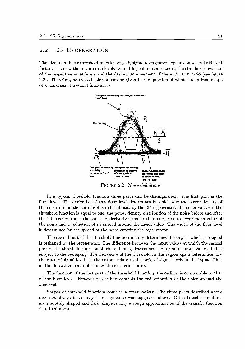
The ideal non-linear threshold function of a 2R signal regenerator depends on several differentfactors, such as: the mean noise levels around logical ones and zeros, the standard deviationof the respective noise levels and the desired improvement of the extinction ratio (see figure2.2). Therefore, no overall solution can be given to the question of what the optimal shapeof a non-linear threshold function is.
Bislopul........,riolc Hil1optl..............probaIliIiIyof pn>boIiI1iIy tiL~~i1\-Z80- tiLh'IIiDco\ ......... .....-"'- -
. ~-Po-,
2
:ltit:lI:Iplurl....-..pobobiIlIy tiL..,.,.,..tiL tnnsIIiaol .....-.....-to •
FIGURE 2.2: Noise definitions
In a typical threshold function three parts can be distinguished. The first part is thefloor level. The derivative of this floor level determines in which way the power density ofthe noise around the zero-level is redistributed by the 2R regenerator. If the derivative of thethreshold function is equal to one, the power density distribution of the noise before and afterthe 2R regenerator is the same. A derivative smaller than one leads to lower mean value ofthe noise and a reduction of its spread around the mean value. The width of the floor levelis determined by the spread of the noise entering the regenerator.
The second part of the threshold function mainly determines the way in which the signalis reshaped by the regenerator. The difference between the input values at which the secondpart of the threshold function starts and ends, determines the region of input values that issubject to the reshaping. The derivative of the threshold in this region again determines howthe ratio of signal levels at the output relate to the ratio of signal levels at the input. Thatis, the derivative here determines the extinction ratio.
The function of the last part of the threshold function, the ceiling, is comparable to thatof the floor level. However the ceiling controls the redistribution of the noise around theone-level.
Shapes of threshold functions come in a great variety. The three parts described abovemay not always be as easy to recognize as was suggested above. Often transfer functionsare smoothly shaped and their shape is only a rough approximation of the transfer functiondescribed above.

22 Chapter 2. The concept
2.3. PRINCIPLE OF OPERATION
As was mentioned in the introduction to this chapter, a form of non-linear thresholdingis required to achieve 2R regeneration. In order to achieve this non-linear thresholding, atechnique is used which is not very different from the one used by E.A. Patent in his work onself-switching Mach-Zehnder Interferometers (MZIs) [2]. The incoming light is redistributedover two different and independent paths in which different non-linear phase shifts are appliedto it. The non-linear, power dependent phase difference now determines how much of thelight is able to pass the threshold (or in E.A. Patent's case, to which output port the light isdirected). The main difference with the work of E.A. Patent is that, in our proposed device,the two fractions of light do not travel through different paths, but in different polarizationstates.
A more elaborate explanation of the principle of operation of the proposed regeneratorwill be given below. The 2R regenerator consists of a series of (partial) polarization convertersand SOAs, as can be see from figure 2.3. To understand its operation it is easiest to onlyconsider the case in which pure TM polarized light is applied to the input of the device. Inthis situation, the light is unequally redistributed over the TE and the TM polarization bythe first partial polarization converter that the light encounters. This polarization converteris indicated by PCj4 in 2.3 to indicate that a fraction of 25% is transferred to the TEpolarization and that a fraction of 75% stays in the TM polarization. In reality this fractioncan be chosen freely, as long as the following conditions are satisfied [2]:
PTE = X%
PT M = 100% - X%
X=l50%
FIGURE 2.3: The 2R regenerator
(2.1)
(2.2)
(2.3)
After being redistributed over the two polarization states by the partial polarizationconverter, the light passes through a SOA. The SOA contains a quantum well under highcompressive strain, causing it to have a high amplification, but only for light of the TEpolarization. Therefore, passing through the first SOA, only the TE polarized light is amplifiedand obtains a TE phase shift, which is dependent on the strength of the optical field and thecarrier density in the SOA.
After having propagated through the first partial polarization converter and the first SOA,the light now encounters a full polarization converter. The full polarization converter causesthe power and the phase of the light in the TE and TM polarization state to be mutually
2.3. Principle of operation 23
exchanged. The light that was first in the TE polarization (and was amplified and phaseshifted) is now in the TM polarization and the other way around.
Again the light encounters a SOA. which is identical to the first one. The fraction that wasamplified by the first SOA. is now TM polarized and therefore not affected by the amplifier.The TE polarized fraction is amplified and phase shifted. After passing through the secondSOA, the light is recombined to a single polarization state by the last partial polarizationconverter. Nota bene: The last partial polarization converter has its slanted sidewall on theopposite side of the converter in comparison to the first partial polarization converter (notethe dark line at one side of the converters, indicating the position of the slanted side). Theoperation performed by the last partial polarization converter is because of this reciprocal tothat of the the first.
The final result of these manipulations of the light is not very interesting at first sight.In the linear regime, the partial polarization converters cancel their individual effect. Inthe SOAs both fractions of the light are amplified and phase shifted equally. The only realconversion is done by the full polarization converter, which causes the light at the output tobe TE polarized. If, however, the power is increased to the non-linear regime, the behaviorof the device changes drastically.
For higher input powers, first only one of the SOAs is able to saturate! and eventuallyboth of them, since they both experience a different fraction of the total power applied to theinput (X% and lOO%-X% resp.). Saturation ofthe SOAs gives rise to a non-linear phase shift.The amount of non-linear phase shift gained in the SOAs is dependent on the carrier densityin the SOA, which is dependent on the level of saturation the SOA is in and is thereforedependent on the amount of power that was applied to the input of the SOA.
The process of polarization conversion inherently introduces a phase shift of 1['/2 radians,while coupling light from one polarization state into the other. After the first partial polarization converter the phase difference between the light in the TE polarization and the TMpolarization is thus 1['/2. After the full polarization converter the phase difference is 1[', nottaking into account the phase shift that the light gained in the SOA. The operation of the lastpartial polarization converter is reciprocal to that of the first, which has the slanted sidewallon the opposite side. The phase shift obtained in the last partial converter is therefore -1['/2radians and the total phase shift after the three conversions (again excluding the phase shiftobtained in the SOAs) is 1['/2 radians.
The process of polarization conversion does not only introduce phase differences. it isalso highly dependent on the phase difference between the light in both polarization states2 .
This, however, is only important for the partial polarization converters and especially for thelast. If the phase difference between the polarization states is not equal to 1['/2 as it wasafter the first partial polarization converter, the conversion is not reciprocal to the conversiondone by the first partial polarization converter. This means that if somehow an additionalphase difference is gained, in our case by the saturated SOAs, the recombination into one
1If a pulse travels through a SOA at rest, it depletes the number of carriers by forcing stimulated emission.As the light moves on the power increases because of amplification and more and more carriers are removed.At a certain point an equilibrium is reached between the carriers added by pumping and carriers removed bystimulated emission. The carrier density stabilizes and the amplifier is in satura.tion. The gain at this level islower than the gain for an unsaturated SOA. The saturation power is defined as the power level at which thegain of the SOA is reduced by a factor 2.
2See Appendix A

24 Chapter 2. The concept
polarization state is not complete anymore3 .
What can be seen now is that for low input power, the SOAs do not saturate and bothfractions of light obtain the same amount of amplification and phase shift. All light is thereforerecombined in the TE polarization state by the last partial polarization converter. If however,(at least) one of the SOAs is saturated, a power dependent phase difference between the twopolarization states is induced and the recombination by the last partial polarization converteris not complete anymore. A fraction of TM polarized light now appears at the output of thedevice.
In addition to this, it is assumed that only TM polarized light can propagate throughwaveguides made of POLIS material without suffering from major losses. Light of the TEpolarization is strongly absorbed. Only if the power of the light at the input is sufficientlyhigh, a fraction of this light will appear at the output in the TM polarization. So the POLISregenerator, in combination with the waveguides, shows the same behavior as a saturableabsorber for TM polarized light.
2.4. STATIC ANALYSIS
To derive the transfer function of the 2R regenerator, the transfer matrix method is used.Transfer matrices are 2-by-2 matrices relating the complex amplitudes of the TE and TMmode at the output of a device to the input (see equation 2.4). The transfer function of the2R regenerator results from the multiplication of all the transfer matrices of the subelementspresent in the regenerator. The output power is then determined by taking the result ofthis multiplication and multiplying it with its complex conjugate. For the sake of simplicity,losses, reflections and other deviations from the ideal situation are neglected in this staticanalysis. This analysis is therefore only meant to explain the principle of operation. In amore detailed study, these factors have to be taken into account.
(2.4)
The transfer matrices of the polarization converters and the SOAs are given by equations2.5 and 2.6. The factor j in the transfer matrix of the polarization converter representsthe 7r/2 phase shift, involved in the process of polarization conversion. Note that the nondiagonal elements obtain a minus sign if the slanted sidewall is placed on the opposite side ofthe converter.
- (vr=x j..jX )Tpc(x) = j..jX vr=x (2.5)
For the transfer matrix of the SOAs, the following assumptions were made. Light ofthe TM polarization passes through the SOA without experiencing any amplification andobtaining a linear phase factor, which is only dependent on the length of the SOA. The TE
3 A detailed example is given in appendix D

2.4. Static Analysis 25
polarized light is amplified and experiences a power dependent phase shift, which is relatedto the gain-saturation by means of the a-parameter.
(2.6)
In this equation, g represents the gain of the SOA as a function of PTE as given byequation 2.7, with Psat the power at which the SOA starts to saturate. ¢ Represents thelinear phase shift obtained by the TM polarization and 'l/J = ¢L + ¢N L the sum of the linearand non-linear phase shift obtained by the TE polarization.
(2.7)
Equation 2.8 gives the relation beween the phase shift and the power, with N the carrierdensity in the SOA and n the corresponding refractive index.
27r an/aN 27r an/aPa = Tag/aN = T ag/aP (2.8)
With equation 2.7 and 2.8 we can express the non-linear phase shift a." 2.9, which reducesto 2.10 if P << Psat . In this equation, the term between brackets represents the differencein gain between the unsaturated and the saturated situation. The difference in gain is thentransformed to a change in phase by multiplying it with the a-parameter.
0' [ go]'l/J(PTE ) = ¢L + 2" go - 1 + Ex..&:.P8al
(2.9)
(2.10)
At this point only a transfer matrix description of the POLIS waveguides is missingin order to properly describe the operation of the 2R regenerator. Since light of the TEpolarization can not travel through a POLIS waveguide without being attenuated by the losses(over 100dB/cm) and since there is almost no absorption for light of the TM polarization weassume that the transfer matrix of a POLIS waveguide is represented by:
- (01
00)TWG= (2.11)
If we now multiply all transfer matrices in the correct order, we end up with a matrixthat has only one element not equal to zero. This is caused by the transfer matrices of the
26 Chapter 2. The concept
waveguides. If we multiply this non-zero element with its complex conjugate, we end up withequation 2.12, which describes the gain of the 2R regenerator as a function of the input power.In this equation 90 is the linear gain per centimeter, Psat is the saturation power in Wattsand <PNL is the non-linear phase difference between the to polarization states given in radians(x = 0.25 in eq. 2.5).
Pout TM 3 [290 290 gQ, gO ]__---'-'- = - el+3Pin.l4P.•at + e 1+Pi.",/4Psat - 2el+3Pin)4Psat e 1+ P",.I4Psat COS(<PNL)Pin,TM 16
(2.12)
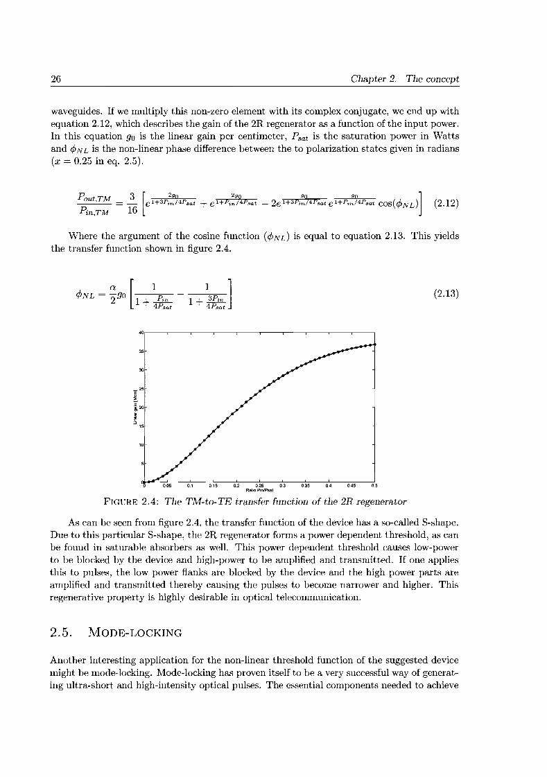
Where the argument of the cosine function (<pN d is equal to equation 2.13. This yieldsthe transfer function shown in figure 2.4.
a [1 1]<PN L = -290 1 p - 1 3F+ ---l.!L. + -.ill..
4Psat 4Psat
40,-----.------.------,------,------,--.-----.------.------,-----,
(2.13)
35
30
10
005 0.' 0.15 0.2 0.25 0.3Ratio PinlPsat
0.35 0.4 045 0.5
FIGURE 2.4: The TM-to-TE transfer function of the 2R regenerator
As can be seen from figure 2.4, the transfer function of the device has a so-called S-shape.Due to this particular S-shape, the 2R regenerator forms a power dependent threshold, as canbe found in saturable absorbers as well. This power dependent threshold causes low-powerto be blocked by the device and high-power to be amplified and transmitted. If one appliesthis to pulses, the low power flanks are blocked by the device and the high power parts areamplified and transmitted thereby causing the pulses to become narrower and higher. Thisregenerative property is highly desirable in optical telecommunication.
2.5. MODE-LOCKING
Another interesting application for the non-linear threshold function of the suggested devicemight be mode-locking. Mode-locking has proven itself to be a very successful way of generating ultra-short and high-intensity optical pulses. The essential components needed to achieve

2.5. Mode-locking 27
passive mode-locking are a cavity with feed-back, an amplifying medium and a non-linear absorbing element. The non-linear absorbing element should be less absorbing at higher opticalintensities and should have a fast response to the intensity of the applied optical field.
The proposed 2R regenerator shows comparable non-linear behavior as the absorbingmedium used to achieve passive mode-locking. This can be seen from the shape of thetransfer function (see figure 2.4), which was derived in the static analysis. Moreover, the 2Rregenerator has the ability to amplify optical pulses as well. An interesting application ofthe proposed 2R regenerating structure might therefore lie in a mode-locked laser. As waspointed out earlier, the 2R regenerator behaves like a saturable absorber for TM polarizedlight. Since it also amplifies the incoming optical signals, the device may replace both theamplifier and absorber in the ring structure of a mode-locked laser (figure 2.5).
[::=J WavegUide
_ Amplifier
.. Polarization Converter
c=J MMI
_ Filter's Register
FIGURE 2.5: The 2R regenerator in mode-locked laser conEguration
Within the mode-locked laser application, the 2R regenerator removes the low powerflanks of the optical pulses traveling through the cavity, thereby reshaping the pulse anddecreasing the pulse width. The total pulse duration is limited by additional effects. Theseeffects include the available bandwidth (see figure 1.7), the self-phase modulation, carrierheating and two-photon absorption. All these effects take place on very small and differenttime scales. In the dynamical analysis, presented in the remaining chapters of this thesis, thepossibility of using the device concept in a mode-locked laser will be investigated as well.
3DEVICE MODELING
3.1. INTRODUCTION
Before the behavior of the 2R regenerator can be simulated, a computer model has to bedeveloped which includes the behavior of the different subdevices and which can simulate thepropagation of light through a series of subdevices. The modeling of semiconductor opticaldevices can be done in several different ways and a distinction can be made between two mainbranches of modeling. One type of modeling concerns the mapping of the optical properties.It involves the calculation of refractive indices, propagation constants, field distributions etc.The information is derived from the material composition and the geometry of the device.This type of modeling is not suitable to investigate the behavior of the 2R regenerator, sinceit does not provide the desired information about the operation of the 2R regenerator.
Another type of device modeling involves the modeling of the response of a certain optical devices to externally applied light. The light can either be continuous wave, represent asignal or represent noise. Often the calculation of the device's response is done by means of aphenomenological representation, instead of taking into account and linking all the physicalprocesses involved. The accuracy of the results obtained with such a model depend on thecompleteness of the model that is used. Several basic techniques can be used to phenomenologically represent the response of the device on a certain form of input. Examples of someof these basic techniques are given in table 3.1.
A static analysis of the 2R regenerator was already performed in chapter 2 of this thesis.In reality a static situation is not applicable to a 2R regenerator, since such devices are usedto reamplify and reshape high-speed optical signals. The main interest now is to investigatewhich parameters have a significant influence on the operation of the regenerator and whichissues occur if the regenerator is used on high-speed optical signals.
The traveling wave model is suitable to investigate the behavior of the response of the2R regenerator to high-speed optical pulses. The next section of this chapter gives a shortoverview about how the traveling wave model works and what implications the use of thismodel has on the modeling of the individual devices. The modeling of devices is discussed inthe remaining sections of this chapter.
29
30 Chapter 3. Device modeling
IApplications:I ConstraintsType of analysis:
Static continuous wave Static P/I curveNo noise >./1 curve
Small-signal dynamics No noise 1M repsonseSmall-signal dynam- FM repsonseics
2nd and 3rd order dis-tortions in FM and1M repsonse
Noise analysis Small-signal dynam- RINics
LinewidthLarge-signal dynamics Noise sources op- Step response
tionalNo sub-picosecond Impulse responsebehavior
Power spectrum op-tional
TABLE 3.1: Modeling techniques([9J)
3.2. THE TRAVELING WAVE MODEL
The traveling wave model has been derived from the Maxwell equations by making severalassumptions and simplifications ([10]). As we know, optical fields are vectorial quantities thatdepend on their spatial coordinates, as well as on time. Their vectorial nature is related to thepolarization of optical fields. In order to describe the spatial dependence of optical fields, anoptical field can be decomposed in basic waveguide modes of the device under consideration.If we assume that the transverse distribution of these modes is not dependent on time or theaxial position z, we can express the spatial distribution of the optical field by means of thespatial distribution of these modes cP(x, y). Since lateral and transverse sizes of active regionsin devices of interest are usually very small, it can be assumed that only the lowest order TEand TM modes are above the cut-off frequency of the waveguide.
In this case, the longitudinal and time dependence of the optical field are representedby z-dependent multipliers in the decomposition. If we now consider the fact that opticalfields propagate in two directions and take into account the assumptions made above, we canexpress the optical field as equation 3.1.
E±(x. y, z, t) = cP(x, y) L A~(z, t)ei (wm t±{3mZ)
m
(3.1)
In this equation, the transverse field distribution is represented by cP(x, y) of the lateralelectrical field of the lowest order eigenmode of the waveguide. Further it is assumed that thetransverse field distribution of this lowest order mode is identical for all longitudinal modes,

3.2. The traveling wa.ve model 31
with mode number m, because their optical frequencies (wm ) are closely spaced. A± Is thecomplex amplitude that represents the slowly varying envelope of the electrical field. All rapidtransitions, of which the frequency lies in the order of the optical frequency, are representedby the exponential factors. (3m Represents the propagation constant of the specific mode.
Every electro-magnetic field has to satisfy the relationships imposed by Maxwell's equations. This, of course, holds for optical fields as well. For isotropic materials, such as semiconductor materials, these equations can be reduced to the wave equation. In our case, thiswave equation can be replaced with a simple scalar form of this equation 3.2, in which E isthe decomposition of the optical field given by equation 3.1, n = n(x, y, z, t) is the refractiveindex structure of the device and F represents the spontaneous emission.
(3.2)
If E represents the decomposition of the optical field, the derived scalar wave equationis still dependent on the spatial distribution of the lowest order eigenmodes of the waveguidecjJ(x, y). In order to eliminate this dependency on the transverse coordinates, we consider thetwo dimensional Helmholtz equation. For every longitudinal mode m, cjJ(x, y) is a solution tothis equation. We can eliminate the spatial distribution by solving the Helmholtz equation.
(3.3)
There are several possibilities to calculate (3m' Often the effective refractive index ne isused to calculate (3m. This is done through the relation (3m = 21rne/ Am, assuming the effectiverefractive index is m-independent. For an active layer with gain, absorption and a refractiveindex which is dependent on the local carrier density, the propagation constant is given by:
(3.4)
In this equation r is the confinement factor of the layer, tln(N) is the change in refractiveindex due to changes in carrier density and g(A, N) and aint represent the gain and theattenuation respectively.
If we now consider the scalar wave equation and take the decomposition of the opticalfield for E, the transverse field dependence represented by cjJ(x, y) can be eliminated by meansof the Helmholtz equation. The final result of the simplifications made above is a coupledmode equation describing the forward (and backward) propagating wave. This equation is:
8A(z, t) ~ 8A(z, t) _ ~r (N E) _ ~. .i21r ( r A (N))8z + v
g8t - 2 g, 2 amt + A ne + un (3.5)
After separation of the real and complex part of this equation, this equation can easilybe solved by any finite difference integration method. The accuracy is then determined by

32 Chapter 3. Device modeling
the amount of discretization of the device under investigation and the completeness of themodel. The limitations of the model used to investigate the regenerator are given in [20]. Themost important limitation of the model is, that it is not capable of simulating sub-picosecondbehavior. This is caused by the simplification of the processes that are involved and whichoperate on a sub-picosecond timescale (e.g. spectral hole burning and carrier heating). Sinceour goal is only to investigate the feasibility of the concept presented in the previous chapterand to determine the key parameters, this model is sufficient for our purposes. The mostimportant design considerations and assumptions, however, are stated in the next section ofthis chapter.
3.3. BASIC OPERATION OF THE SOFTWARE
In the modeling software, the total device cavity (the waveguides, SOAs and polarization converters) is represented as a large array of 2000 elements. Per element the program keeps trackof the power, phase and functionality of the element. Depending on an integer value, whichrepresents the functionality of the element, the program switches to a routine to calculate thepower and phase of the light at the output of the specific element as a function of the powerand phase at the input. The power and phase at the output of the element are then storedin a buffer array.
After having performed this integration for all elements in the array, the power and phasestored in the buffer array are shifted one position in the appropriate direction (to represent thepropagation of the light) and are used as the input power and phase of the element at whichthey have now arrived. The shifting is repeated as long as is necessary to let each element(containing power and phase) of the applied input field pass all elements in the software, andthus pass the complete device represented by the array.
The elements at the beginning and at the end of the array have special functions to couplethe "light" at the input into the array and at the end, out of the array. If necessary, the inand out-coupling of the light is performed coherently. Because of the coherent coupling, thesoftware is also capable of simulating the situation in which light makes multiple round-tripsin a circular cavity. Every round-trip a fraction of the light is (coherently) coupled (in and)out of the "cavity" by the array element that closes the circular "cavity". This is similar toa circular cavity containing an "MMI" (Multi-Mode Interferometer).
Per function implemented in the software (SOA, waveguide, polarization converter, etc.) aset of differential equations is included in the program. These sets of differential equations arethe rate equations and phenomenologically describe the response of one of the array elementson specific values of input power and phase.
3.4. DESIGN CONSIDERATIONS
GAIN SUPPRESSION
Although it is often assumed, gain in SOAs and lasers is not merely dependent on the densityof carriers in the active volume. It is dependent on the wavelength and photon density as

3.4. Design considerations 33
well and the previous assumption is only valid as long as the distribution of carriers in theconduction band and valence band is equal to the equilibrium distribution.
Under normal circumstances, if an SOA is biased far above threshold, the stimulatedemission and absorption are limited to a certain number of discrete wavelengths. Under thesecircumstances the interaction of the light only takes place with carriers of the appropriateenergy levels. This leads to a disturbance of the thermal equilibrium distribution of carriersin both bands. This disturbance is called Spectral Hole Burning, referring to a depletion ofgain for specific, well-defined wavelengths.
The timescale on which the disturbance of the spectral carrier distribution occurs lies inthe order of 10-14 and 10-13 seconds. The disturbance is overcome as the empty states arefilled with electrons from neighboring states through intraband collisions. Even though thetime-scale on which the Spectral Hole Burning occurs is very short, it still affects the gain ofthe material.
A similar process to Spectral Hole Burning is Carrier Heating. Carrier Heating is causedby the stimulated recombination of carriers with an energy below the quasi-Fermi level. Because of the loss of these "cold" carriers, the average "temperature" of the remaining carriersincreases. This non-thermal distribution is restored by this increase in temperature of theremaining carriers.
The disturbances of the carrier distributions by Spectral Hole burning and Carrier heatingcan be represented by rate equations. The exact contribution of both processes, however,is not known. In the simulation software, their combined effect on the gain is thereforerepresented by a certain parameter, the so-called "gain-suppression-parameter" ESHB (seeequation 3.7). The representation of the gain, given by equation 3.6 as a function of carrierdensity (N), energy (E) and photon density (S), is valid as long as the simulation time-scaleremains well above the time-scale of these processes. If these processes are to be representedon their real time-scale, rate equations like equations 3.8 and 3.9 can be used to account forthe correct behavior of the carrier density and gain at a certain energy level.
(3.6)
(3.7)
(3.8)
(3.9)
LINEWIDTH ENHANCEMENT FACTOR
In laser diodes, both the gain 9 and the refractive index n change with the average quantumwell carrier concentration N. The relationship between how the gain and the refractive index
34 Chapter 3. Device modeling
are affected by a change in carrier density, can be described by the ratio of the independentchanges. This is referred to as the linewidth enhancement factor. It typically has a valuebetween 4 and 6 for semiconductor lasers ([4]) and is dependent on the wavelength and, forquantum well material, on the carrier density ([11]).
271" dn/dN0: = - - -.:..,--
>'0 dg/dN(3.10)
Linewidth enhancement expresses itself in the regenerator as a phase change caused bya change in carrier density. The change in carrier density, in its turn, is caused by theamplification or absorption of light in the active volume. The linewidth enhancement factoris important to the concept of the regenerator because it determines the amount of phaseshift an optical pulse will obtain during its propagation through the SOAs. In the model twodifferent linewidth enhancement factors are used. The carrier linewidth enhancement factorand the temperature linewidth enhancement factor. The first referring to normal changesin carrier density, the latter representing changes in carrier density caused by processes asspectral hole burning and carrier heating.
POLARIZATION MODE DISPERSION
Integrated waveguides, even though they were designed to be single mode, are not truly singlemode because they can support two optical modes which are polarized in two orthogonaldirections. This results in slightly different propagation constants for the modes polarized inthe x and y direction. This effect is referred to as birefringence.
The axis with the highest refractive index is considered to be the slow axis, since thegroup velocity of the light is higher on the axis with the low refractive index. In standardwaveguides, the beat-length1 La is not constant along the waveguide, but changes is a randomway. This is harmless for continuous wave light, but it becomes an issue if the waveguide isused for the transport of ultra-short optical pulses.
If a certain input pulse excites both polarization states, the light in the two states travelswith different group velocities. The pulse becomes broader at the output of the waveguide,since the group velocities change in a random fashion. This phenomenon is known as Polarization Mode Dispersion. Because of the square root dependence of the PMD-induced pulsebroadening, the dispersion due to randomly changing birefringence is often much smaller thangroup velocity dispersion.
Even although PMD can have a significant influence on the propagation of short opticalpulses, it was not taken into account in the computer model, at least, not everywhere. Thereason that PMD was not included in the model is that the device is symmetric around thefull polarization converter in the middle of the device. Therefore, the light travels an equaldistance in the TM polarization as it does in the TE polarization. In the subdevices in whichthe polarization state and phase are important, the appropriate behavior was included in therate equations describing the device. For the waveguides that form the input and output
IThe beat length describes the length required for the polarization to rotate 360 degrees. For a givenwavelength, it is inversely proportional to the fiber's birefringence.
3.4. Design considerations 35
of the device, PMD does not have to be included either. In these waveguides, the phasedifference between the polarization states is not important anymore and TE polarized lightis strongly absorbed.
POLARIZATION DEPENDENT AMPLIFICATION
Interaction of the light with material that contains one or more strained quantum wells isdependent on the polarization state of the light. In POLIS material the strain applied to thequantum well has deliberately been made as high as possible to limit the interaction of thelight and the material to the one polarization. This polarization is the TE polarization. Sincethe amount of strain applied to the material is so large, it can be assumed that there is nointeraction with the other polarization state ([24]). This has several consequences that haveto be taken into account while modifying the rate equations that are used in combinationwith the traveling wave model, to represent the behavior of POLIS devices.
In the final model only the rate equations for the gain contain the term that describesamplification. As a result, the term that represents the stimulated emission in the carrier rateequation is only dependent on the intensity of the light in the TE polarization. Therefore,any phase changes caused by a change in carrier density, apply only to the TE polarization.The SOA rate equations that describe the behavior of TM polarized light, only consist ofloss terms. The phase of the TM polarization is only influenced by cross-coupling originatingfrom the Kerr effect.
THE KERR EFFECT
Optical power in the semiconductor waveguides can alter the index of refraction. The combined resulting effect of the different power dependent phase changes, is generically calledthe "Kerr effect". In general. the Kerr effect induce a phase modulation on the signal thatis proportional to its instantaneous power level. The phase modulation can then convertedto amplitude modulation by waveguide dispersion. If a waveguide is linearly birefringent,which means that it has two principal axes along which the waveguide is capable of maintaining a state of linear polarization if there are no non-linear effects present, the non-linearcontributions to the refractive index are given by:
(3.11)
(3.12)
The physical meaning of both terms on the right hand side of the equations presentedabove can be explained as follows: the first term represents the self phase modulation andthe second term describes the cross phase modulation. The cross coupling term induces anon-linear coupling between the field components Ex and E y .
36
3.5.
Chapter 3. Device modeling
MODIFICATIONS TO THE ORIGINAL MODEL
The original implementation of the traveling wave model, realized by Y. Barbarin and E.A.J.M.Bente included power and phase changes of the light in a device, caused by the processes described in [20]. This implementation was capable of simulating the propagation of light in twodirections, but no representation of polarization nor a polarization dependent response of thedevices was included. In order to make the model suitable to simulate the behavior of the 2Rregenerator the model had to be extended accordingly. Therefore the following modificationshad to be made to the original model:
• Add a representation of two orthogonal polarization states of light (TE/TM) 2
• Include appropriate device behavior for TE/TM polarized light
• Develop a model for polarization conversion
The implications of these modifications to the original model are as follows. For all devicesa set of nine differential equations has to be specified. This set of equations includes fourequations describing the change in power for two polarization states and in two directions. Itincludes one single equation that describes the change in carrier density. Only TE polarizedlight will have an influence on the carrier density, but light travels in two directions, whichdeserves special attention. Finally there are four differential equations that describe the phasechanges of the light for two polarizations and for two directions.
Since there are now nine different variables to keep track of, which are continuouslychanging during the calculation of one round trip of the light through the device cavity, anequal amount of arrays has to exist in order to be able to store these variables. Some of theparameters that are used by the different sets of rate equations are polarization dependent.The total number of parameters specified in the input file is therefore doubled. The parametersoccur once for each polarization. Parameters that are not affected by a change in polarizationare represented once.
Next to changes in the architecture of the software, the rate equations have to be modified as well, in order to have them represent the correct behavior of the devices. Thesemodifications are discussed in the next section of this chapter.
3.6. SEMICONDUCTOR OPTICAL AMPLIFIERS
INTRODUCTION
Ever since their first implementation, SOAs have been subject of considerable research interest. This is because their carrier dynamics are important for the understanding of high-speedmodulation of semiconductor lasers, as well as for optimizing devices for applications such aswavelength conversion and optical switching. All these different application areas of SOAshave led to a wide variety of architectures and technologies. They have been implemented inmany different material systems with bulk material, as well as with quantum wells and, since
2See Appendix A

3.6. Semiconductor Optical Amplifiers 37
recently, with quantum dots. Every single variant having its own advantages and disadvantages for particular applications over the other variants.
In the past SOAs have proven themselves very useful in providing gain as well as phaseshift. Both of these capabilities are exploited in the 2R regenerator. In this concept the SOAsserve to amplify the signal and to generate a relative phase shift between the light in twopolarizations, which is proportional to the power of the incoming signal. This phase shift willthen be used to influence the recombination by the last partial polarization converter in the2R regenerator, thereby imitating the effect of interference.
MATHEMATICAL DESCRIPTION
The mathematical description of the processes governing the propagation and amplificationof optical pulses in an SOA as derived by Tang and Shore in [20], is presented by equations3.13 and 3.14. In this paper the describing system of equations is expressed in terms of powerand gain. These equations have to be rewritten to yield the change in photon density, carrierdensity and phase for the computer model of the 2R regenerator. The derivation of the newequations is discussed below. Beside the rewriting of the equations, the considerations madein the previous paragraph are immediately taken into account.
aA(z, t) + ~ aA(z, t) =az vg at
1 g(N) A(z, t) _21 + tIP
t [aNg(N) - aT EI9(N):] A(z, t) -2 1 + EI
(jrKerr :0 n2) P A(z, t) - ~aintA(z, t) (3.13)
In this equation A(z, t) is the amplitude of the envelope of the optical pulse, and P =IA(z, tW is the power of the pulse. aN and aT are the carrier and temperature linewidthenhancement factors, n2 is the non-linear refractive index related to the Kerr effect, rKerr isthe confinement factor of the Kerr effect, wo, c and aint are the optical frequency, the speedof light and the internal absorption respectively. The gain g(N) is given by 3.14.
ag(N) = g(N) - go(N) __1_ g(N) Pat T s E sat 1 + EIP
(3.14)
In order to rewrite the equations 3.14 and 3.13, the following relations have to be defined.9 represents the gain as a function of the carrier density. go is the small signal gain, with thepump factor Wpump the amount of carriers injected by an external current source. (T is theeffective active cross-section. P is the optical power as a function of photon density SandE sat is the saturation energy of the SOA as a function of material gain.
(3.15)

38
IWpump = V;q. act
Aact0"=--r
P = ShwvgO"
Chapter 3. Device modeling
(3.16)
(3.17)
(3.18)
(3.19)
(3.20)
Using the relations presented above and using equation 3.21 between the gain and thecarrier density in the SOA, we can transform the derivative of the gain in the derivative ofthe carrier density.
dN 1 dN dg(N) 1 dg(N)dt = r dg~ = raN .~
(3.21)
dN
dt
I N 2 3 aNrvgNo In (fi )-- - - - BN - CN - S 0
q' Vaet Ts 1 + Elhwvg Arct S(3.22)
From the derivative of the carrier density, it can be seen that it is fed by Wpump
1/qVact ' Carriers are removed from the reservoir by various processes. Among these processesare the so-called Shockley-Read-Hall recombination, by spontaneous emission (BN2 ), Augerrecombination (CN3 ) and by the simulated emission. Equation 3.22 is the equation used inthe simulation software and S = STE CW + STE ccw3 •, ,
The same can now be done to transform the power rate equation in a photon density rateequation:
dP
dtg(N)P P1 + EIP - Oint
(3.23)
3Two counter-propagating waves can cause a standing wave. If this occurs in the SOAs, the carrier distribution inside the SOA changes according to the standing wave pattern. This is known as spatial hole burningand can cause reflections, since the carrier density, and thus the refractive index, changes regularly and canform a "grating"

3.7. vVa.veguides 39
Using equations 3.15 to 3.20 and substituting them in the power rate equation. we findequations 3.24 and 3.25:
Loss} . L seg _NLosS2 . L seg +Brf3N (3.24)Jrseg Jrseg
dSTM,CW = _ Loss} . Lseg _ NLosS2 . L seg
dt 'Tseg Jrseg(3.25)
As can be seen from these equations, only TE polarized light is provided with gain. TMpolarized light is attenuated. The saturation of the gain is caused by light traveling in bothdirections. The equations for the backward traveling waves are exactly the same.
The last equations to be modified in the model is the phase equation:
(3.26)
Again, a distinction is made between TE and TM polarized light, according to the considerations presented in one of the previous sections. Only TE polarized light obtains a carrierdensity related phase shift. Another important aspect is the cross phase modulation, whichis caused by the Kerr effect. This implies that at high optical intensities, the light in onepolarization state influences the refractive index experienced by the other polarization state.Again, the equations for the backward traveling optical field are exactly the same.
(3.27)
(3.28)
3.7. WAVEGUIDES
Closely related to the SOAs are the POLIS waveguides. Waveguides are used to connectthe different optical components on a chip. In the POLIS concept they have an additionalfunction, namely polarization filtering. As was pointed out before, SOAs and waveguidesare nearly transparent for light of the TM polarization and light of the TE polarization isstrongly absorbed by interaction with the quantum well. The absorption of the light with thequantum well leads to generation of free carriers, which will change the refractive index andtherefore the phase of the light which is passing through the waveguide.
In the 2R regenerator the waveguides only have a minor influence on the operation of thetotal device. For this reason, and in order to cut the computational effort required, the losses

40 Chapter 3. Device modeling
in the waveguides are represented as passive losses, meaning that the power is attenuatedwith a constant factor in each element and that no carriers are generated nor the phase ofthe light is influenced.
In some cases it is necessary to include the losses in the waveguides more elaborately, forexample in the case of polarization converters. In such cases, the waveguides can be modeledas unpumped SOAs. The losses are then represented by the rate equations, which also takecare of proper representation of any carrier generation and phase changes. The rate equationsrepresenting the losses can simply be added to the equations describing other processes inthat specific element (such as polarization conversion).4
4 Attention has to be paid when choosing the "gain" or rather attenuation for these sections. Since thesesections are unpumped, there are no carriers present and the logarithm in the gain term (No In N / No) isapproximately equal to -5, leading to a much higher absorption than desired if not taken into account.

4POLARIZATION CONVERTERS
4.1. INTRODUCTION
Polarization converters play a very important role within the POLIS concept. The highpolarization dependent absorption of the material creates the possibility to create active andpassive functions with a device that is capable of switching between the TE and the TMpolarization. In the 2R regenerator the polarization converters are used to switch betweenthe TE and TM polarization or to (partially) redistribute the light over the two polarizationstates. This creates the possibility to manipulate the light in both polarization states almostindependently and to take advantage of the polarization dependence of the material.
Since the behavior of the 2R regenerator is investigated by means of a computer model,this model should have the capability of simulating the behavior of optical pulses in polarization converters as well. Within the POLIS concept, the behavior of a polarization converteris more complicated, since the material has high losses for one of the main polarization states.This strongly influences the response of the converter on the incoming light. Therefore theselosses have to be incorporated in the model for the polarization converter.
The computer model uses sets of differential equations to describe the behavior of thedifferent types of optical components. The most common example of such differential equ~tions, are the rate equations for a SOA or laser. The behavior of a polarization convertercan be described in several different ways, e.g. by coupled-mode theory and by the transfermatrix method. However, no description of polarization conversion by means of rate equations existed. To be able to include polarization conversion in our computer model, a set ofdifferential equations was derived from the coupled-mode theory.
4.2. POLARIZATION CONVERSION
The polarization converters used in the POLIS concept are so-called slanted sidewall polarization converters. These converters operate on the principle that the light is forced into twohybrid polarization states, which are linear combinations of the main polarization states TEand TM. The fraction of TE polarized light and TM polarized light in the two hybrid modes
41

42 Chapter 4. Polarization converters
is dependent on the angle at which the two hybrid modes are placed with respect to the TEand TM polarization. This angle can be influenced by the angle of the slanted sidewall andthe width of the converter waveguide.
The optimal tilt angle of the modes is 1r/ 4 radians and occurs a width of 0.82 pm [29]. Atilt angle of 1r/ 4 radians implies that the tilted modes consist of equal TE and TM parts. Onepolarized tilted mode is dominantly polarized along the slanted interface, while the secondtilted mode is polarized perpendicular to that interface. Assuming that the waveguide profileis such that the hybrid modes are well confined and the effective refractive index differencebetween the modes is much less than the effective index difference between these modes andthe lowest order radiation mode, the amplitudes of the spatial field distributions are almostidentical.
(a) (b)FIGURE 4.1: Polarization converters
It is assumed that both tilted modes experience different propagation constants and dephase while propagating through the converter waveguide. At the end of the polarizationconverter light in the tilted modes is forced back in the TE and TM polarization. The fractionof light in both polarization states is determined by the phase difference the light gained whilepropagating in the tilted modes. The coupling process between the two orthogonally polarizedmodes, which occurs in the polarization converter, can be described by means of the coupledmode theory.
4.3. MATHEMATICAL DESCRIPTION
The coupled mode theory applies in a large class of coupled mode interactions, where thereare only two guided modes that possess sufficient phase synchronism to allow a significantexchange of energy. Therefore, one can neglect all other modes and obtain simple coupledwave equations that describe the interaction between these modes. Solutions to the coupledwave equations are well known and have been derived in several ways in literature.
The coupled mode theory distinguishes between two different types of interactions, codirectional interactions and contra-directional interactions. Co-directional interactions occurbetween two forward (or two backward) propagating modes, and contra-directional interactions occur between a forward and a backward running mode. To be more precise, it is therelative direction of the group velocities of the modes that is considered here. In the case ofthe polarization converter we deal with co-directional interactions first and call the amplitudes

4.3. Mathematical description
of the two significant waves ATE and ATM ([5]).
dATE(l). .dl = -Jf,,ATM(I) +]<5ATE (I) - aTEATE(I)
43
(4.1)
(4.2)
In these equations the variables ,.." a and <5 represent the coupling constant, the TEattenuation and the phase mismatch respectively. From these coupled mode equations wewant to derive a set of differential equations in terms of power and phase, since this is thetype of equations used in the rest of the model. In order to transform the coupled modeequations to a set of real, differential equations, we first perform the following substitutions.
ATE(I) = VPTE(l) . ei¢(l) (4.3)
(4.4)
This substitution leads to the following set of complex equations, from the real andimaginary parts of which four new and independent equations can be derived.
Two of these equations represent the change of power of the two polarization states, theremaining equations describe the phase change of the light. The equations are given by 4.7to 4.10.
PTE(l) V .dl = 2,.., PTE(l)PTM (I) sm(1jJ(I) - ¢(l)) - 2PTE(I)a (4.7)
(4.8)
d¢(I)----;n:- = -,..,PTM(I)PTE(I) cos(¢(I) -'ljJ(l)) + <5 (4.9)

44
d'lj)(l)-- =-1'\,
dlPTE(l) cos(¢(l) - 'ljJ(1)) - 8PTAf(l)
Cllapter 4. Polarization converters
(4.10)
Before the equations 4.7 to 4.10 can be used in the computer model, a minor changehas to be made and a missing parameter has to be defined. The change that has to bemade to the equations is caused by the fact that the absorption, most likely, is not constant.Incorporating the non-constant losses for the TE polarization state can easily be done byreplacing the factor aTE in equation 4.7 with the differential equation that describes theabsorption in the quantum well. The other differential equations, representing the changes inTM power, phase and carrier density then have to be added to their equivalents, describingpolarization conversion, as welL
The presence of the quantum well in the polarization converter waveguide, has anotherundesirable effect, as we will see. If light passes through a quantum well layer, it generatesfree carriers, as is inherent to the absorption of light by the well. If the amount of free carriersin the well is high enough, they cause a refractive index change and therefore they have aninfluence on the phase of the light. Since the phase of the light is very important in thepolarization converter, any phase changes caused by free carriers have to be incorporated tothe model as well. To achieve this, the differential equations describing a phase change dueto carrier or temperature linewidth enhancement, are added to the differential equations thatdescribe the phase change due to the polarization conversion process.
Now that the minor changes have been made to the model, the only thing left to do isdefine the coupling constant of a converter section. The coupling originates from a phasedifference that increases along the way, when the light is propagating through the converter.A phase changes of 271" leads to zero net conversion. The length of the converter for whichzero net conversion occurs, is called the beat length. The coupling constant is now defined asa function of this beat length, 13Mo and 13Ml represent the effective propagation constants ofboth tilted modes.
71"LB = I'\, = 13M1 - 13Mo (4.11)
In the next sections of this chapter, the influence of the coupling strength, the absorptionand phase mismatch on the conversion efficiency is studied. To perform the simulations,arbitrary values could be taken for these parameters. However, to stay as close to reality aspossible, the length of the polarization was chosen to be close to 125 11m. In the travelingwave model, the converter will be modeled by a series of elements. Each element represents,as we will see in chapter 5, a time span of 25 fs. If we assume that the POLIS materialhas an effective refractive index of 3.4 in the converters and take the speed of light equalto 300.000 km/s, the length of the converter is passed in 1.42 ps, which corresponds to 56.7elements. For simplicity reasons, the converter length has been chosen to be represented by56 elements in the computer model. After passing through these 56 elements, the light inthe two polarization states has to be fully exchanged. With the help of equation 4.11 we findthat I'\, = 12724.77 . 10-6 11m-1.

4.4. The ideal polarization converter
4.4. THE IDEAL POLARIZATION CONVERTER
45
Simulations of an ideal polarization converter, with the model derived in the previous paragraph, show that the device transfers all power in one polarization state to the other polarization state (fig. 4.2). The conversion efficiency is defined as the ratio between the fractionof light in the opposite polarization state from that at the input and the total amount ofoptical power appearing at the output of the converter and it can be seen that the couplingis reciprocal.
From figure 4.2, we can also see that the light experiences a phase jump of 7f/2 radians, which is inherent to the process of polarization conversion. Reciprocity requires thatlight entering the polarization converter from the other side undergoes the exact oppositetransformation. This means that the sign of the phase shift for polarization conversion in theopposite direction is inverted. In the computer model this functionality has been implementedby adding a second set of four differential equations, with opposite signs to the ones derivedin the previous paragraph.
The phase condition of the light is of particular importance for the last partial polarizationconverter. In order for the 2R regenerator to be completely transparent for light, the fractionsof light in both polarization states need to have a relative phase difference of 7f/2 with eachother. For low input power levels, both polarization states have a relative phase difference of7f radians as soon as the light arrives at the last partial polarization converter. The additionalphase shift required to reduce this (at least partially) to 7f/2 is caused by the gain saturationin the SOAs for higher input power levels.
)0;12<2<1o 50 100 150 200 250
Distance along polarization converter [jlm]
o 50 100 150 200 250Distance along polarization converter [jlm]
FIGURE 4.2: Perfect polarization conversion
4.5. POLARIZATION CONVERTERS WITH LOSSES
Now that the derived model shows the appropriate behavior for an ideal converter, a closerlook can be taken at the effect of introducing imperfections, such as losses and a phase mismatch. Introducing losses for one polarization state leads to different polari,,;ation conversion

46 Chapter 4. Polarization converters
for pure TE and TM polarized light in the polarization converter. This difference is causedby the fact the the polarization dependent losses enhance the conversion in one situation andcounteract the conversion in the other. Fixed (passive) losses translate to a damped sinefunction, because, by approximation, the solution to such a differential equation is an exponentially decaying function, superimposed on the sine shape of the polarization conversion.
In reality the losses occurring in the POLIS polarization converters are not constant. Thelosses are caused by the interaction of TE polarized light with the material of the quantumwell. This interaction is comparable to optical pumping; it causes the TE polarized light to beabsorbed and free electron-hole pairs to be generated. This process affects the local refractiveindex and absorption of the material and is saturable.
In the case of TE light being applied to the input of the converter, the decrease inpower is faster, since light of this state is immediately absorbed. Light is removed fromthe TE polarization by the conversion process, as well as by absorption. Full conversion toTM therefore requires a shorter converter length. In the case of TM light being applied tothe input, there is initially no interaction with the quantum well and the light is convertednormally. Light is transferred to the TE polarization, but is immediately absorbed. Thebuild-up of the TE polarized mode is hindered by the absorption and full conversion requiresa longer converter length in this case.
An example of polarization conversion with losses for one polarization state is shown infigures 4.3(a) and 4.3(b). These figures were obtained with Matlab, using the exact samesystem of differential equations as are used in the mode-locked laser simulation software. Themodified mode-locked laser software is capable of performing the same simulation, extractionof the appropriate data, however, is not convenient.
One can see clearly from the figures that the damped conversion curve is not the onlydifference with the case of a perfect polarization converter. The locations of the TE/TMmaxima and minima differ from each other, depending on which polarization state is appliedat the input of the converter, so does the location of the characteristic 7r/2 phase jump. Fromthis it can be concluded that attention has to be paid when optimizing the length of thepolarization converters to the required input polarization and to the level of absorption.
4.6. POLARIZATION CONVERTERS WITH A PHASE MISMATCH
Another important phenomenon occurring in polarization converters is a phase mismatchbetween the two polarization states. This mismatch is caused by deviations in the transversalgeometry of the device. While propagating through the polarization converter a linear phasedifference builds up. as a result of the phase mismatch. The result of this phase mismatchcan be seen from figure 4.4.
From figure 4.4 it can be seen that if the tilted modes in the polarization converter are notphase matched, the conversion is not complete. What can be seen from figures 4.2 to 4.3(b) isthat the point of optimum conversion is marked by a phase jump of the light in the convertedstate. For cases in which the distribution of light over the two polarization states is fixed,this phenomenon can help to determine the optimum length of a converter by simulating itsbehavior with the MATLAB model. In the case of a converter with a phase mismatch thepoint of optimum conversion is not so obvious. The phase behavior has been distorted and

4.7. Power dependence of quantum well polarization mode converters
o 50 100 150 200 250Distance along polarization converter [J.tm]
! -~! ! ::'1 ' 'i' , , , , 'j~ -2 """' .. ' .. ," '.""'" '.""'" ',""'"m ...,&. -3 ."."':'".".,:.,, ... , ,', , , . ' . ' ,', , , ... ,
o 50 100 150 200 250Distance along polarization converter [J.tm]
(a)
iO':I~~]o 50 100 150 200 250
Distance along polarization converter [J.tm]
~ -~! ~ ! ;'j ! l*-2········'······'·······'·············,
&. -3 _.... , , ':' . , , .. , ':' ' , ' , , . ~ '.' , , , , , :' ... ' .. :
o 50 100 150 200 250Distance along polarization converter [~m]
(b)FIGURE 4.3: Lossy conversion, TE input (a) and TM input (b)
47
operation is strongly influenced by the chosen length of the converter, which can be seen infigure 4.5(a) and 4.5(b). in which the combined effect of absorption and a phase mismatch isshown. This combined effect is that the conversion is further deteriorated with respect to theseparate effect of absorption and phase mismatch.
4.7. POWER DEPENDENCE OF QUANTUM WELL POLARIZATION MODE
CONVERTERS
In the previous section all the different effects occurring in a non-ideal polarization converterswere first treated separately and then combined in order to represent the real behavior of thedevice. Let us now combine the equations found in chapter 3, about the modeling of SOAs,with equations 4.7 to 4.10 in order to represent the behavior of a polarization converter that

48 Chapter 4. Polarization converters
;"~.:::~ 1 : ~. ~, .-:-' ~ ::. :, ..~ .. ~ "~' .. ,3: 0 5 .: ; > -:o . "',.... : ,...... : .a.. 0 . -:-- ,;..;. ..
o ~ 100 1~ 200 2~
Distance along polarization converter ~m]
i5'~Q) -2l/)CtI
'&.. -4
o
.......:- ..... "~..... ,~. '.~'.<:.' .:....:.. ·1····"~
. '. '., •• 1.
............................::::;:::( :~.:
50 100 150 200 250Distance along polarization converter ~m]
FIGURE 4.4: Conversion with phase mismatch
contains an active layer. Then, by means of optical pumping, carriers can be generated andthe refractive index can be changed. This can be achieved by simply adding the equationscorresponding to the same power and phase. The equations for the carrier density in thepolarization converter remains unaltered, except for the fact that the term that describespumping by current injection is assumed to be zero.
Figure 4.7 show that conversion is not merely dependent on the input polarization state,but on the input power level as well. Figure 4.7 shows the response of a full converter asfunction of power for two cases. In the first case TM polarized light is applied to the input.As we saw from figure 4.3(b), the effective conversion length is longer as absorption for TEpolarized light is included. The conversion is therefore sub-optimal for low input powers.As soon as the level of input power rises, the absorption is saturated and the conversionapproaches the ideal situation, with a larger extinction ratio for TE and TM. The samepoint of view can be applied to the other situations for low input power, the behavior of theconverter corresponds to that of a converter with absorption for one polarization, whereasif the power increases, the behavior becomes comparable to that of an ideal converter (i.e.without absorption).
To our best knowledge, the power dependent behavior of 'quantum well polarization converters has never been investigated before. It is therefore very interesting to see if measurements can verify the predictions based on the computer model. Even if it appears that theeffect is not noticeable, the measurements are still useful. The computer model of the modeconverters can then be simplified in order to reduce the computational time. To study thepower dependence of mode converters, three samples were considered which contained thesame set of polarization converters. The mode converters fabricated on the different samplescontained no quantum well (double hetero material, MO-166), one quantum well (MO-411) ortwo quantum wells (MO-412) respectively. The measurements on these samples are describedin the next section of this chapter.

4.7. Power dependence of quantum well polarization mode converters 49
jo:~do 50 100 150 200 250
Distance along polarization converter w.m]
25050 100 150 200Distance along polarization converter [11m]
! :[ IGJ·········=s·-Ed-lG 0 : : .~ .~ .
-2o
(a)
jo:l~jo 50 100 150 200 250
Distance along polarization converter [11m]
::0~ 0 r-..........,,~..:....;:... .:...:....~ .«l
lG -2~
~ -4 L...-__.........__----'- "---__--'-__---l
o 50 100 150 200 250Distance along polarization converter [11m]
(b)FIGURE 4.5: Lossy conversion with a phase mismatch, TE input (a) and TM input
(b)
MEASUREMENT SETUP
The setup used to carry out the measurements on the quantum well polarization converters,is a so-called transmission setup. This kind of setup is used to investigate integrated opticaldevices that are incapable of generating light. A schematical overview of the setup is givenin figure 4.8.
The setup includes a tunable continuous wave (CW) laser. The output of the CW laser isfed to a powerful EDFA. This combination resulted in the power spectrum shown in 4.7 andoutput power levels up to 18 dBm measured at the output of the EDFA. The output powercan be varied by means of the computer controlled attenuator. Now that we have a lightsource and can control the amount of power going in the chip, the polarization state needsto be controlled. This is done by the polarization controller, indicated by the three black
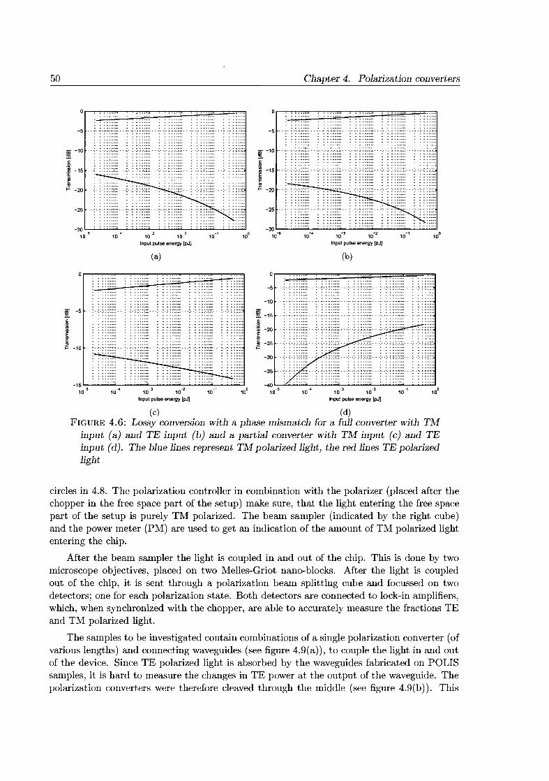
50 Chapter 4. Polarization converters
-5 .....••.•.... -5 .........•......-.•..•..._ - _ ,--
10-<-3~OL..·5---10~··---10~·3---10~·'---10~·'-- .....100
Input pulse energy [pJ]
. :..:.;;:;:.::;:. ,,: .
! -10 .
.~ -15
.~
l!'.... -20
. .. .-30 L..-;...;..;.;.;.;.;.;"--;...;..;..;.;.;.;."--;...;..;..;.;.;.;."--;....;..;..;.;.;.;."--;....;..;~
10-5
-25 .. . ~ .:. :.:~::: ...:. ~.:: :.:::: .. ' ..' .• n'" ..
in -10 ... , ........•.•:E.
.~12 -15 ...~
l!'.... -20 .
(a) (b)
o,............,....,..........,........,.-,.,.,........,........,,..,..,.......,........,,..,..,.......,........,,..,..,.~
... _ .
. . .-5 ,
-10 .. -- .
in -5 ' ...........•.,.:E.§'u;
I!E. -10 .. ~. ~ " " .", ·.~·.·.·r
-15'-:-_-~--'----'----'------'10" 10" 10'3 10" 10" 10°
Input pulse energy [pJ]
in:E. -15 ....•.....•...
§.~ -20.~
~ -25
-30
-40 L..-""-_"--__"--__"--__"--_---'
10'5 10-' 10'3 10" 10" 10°
Input pulse energy [pJJ
(c) (d)FIGURE 4.6: Lossy conversion with a phase mismatch for a full converter with TM
input (a) and TE input (b) and a partial converter with TM input (c) and TEinput (d). The blue lines represent TM polarized light, the red lines TE polarizedlight
circles in 4.8. The polarization controller in combination with the polarizer (placed after thechopper in the free space part of the setup) make sure, that the light entering the free spacepart of the setup is purely TM polarized. The beam sampler (indicated by the right cube)and the power meter (PM) are used to get an indication of the amount of TM polarized lightentering the chip.
After the beam sampler the light is coupled in and out of the chip. This is done by twomicroscope objectives, placed on two Melles-Griot nano-blocks. After the light is coupledout of the chip, it is sent through a polarization beam splitting cube and focussed on twodetectors; one for each polarization state. Both detectors are connected to lock-in amplifiers,which, when synchronized with the chopper, are able to accurately measure the fractions TEand TM polarized light.
The samples to be investigated contain combinations of a single polarization converter (ofvarious lengths) and connecting waveguides (see figure 4.9(a)), to couple the light in and outof the device. Since TE polarized light is absorbed by the waveguides fabricated on POLISsamples, it is hard to measure the changes in TE power at the output of the waveguide. Thepolarization converters were therefore cleaved through the middle (see figure 4.9(b)). This

4.7. Power dependence of quantum well polarization mode converters
or--.-----~----.--..----...,....-___,_--.____,
-5 .
-10 : : :.
_ -15 .ElD
~ -20 ....
i0.. -25
-30 .
-35 .
-40 L...-.L...-....1549.6 1549.8 1550 1550.2 1550.4 1550.6 1550.8
Wavelength [nm)
FIGURE 4.7: The spectrum of tunable laser - EDFA combination
51
I Laser I 0 I EDFA·11 Atten.
FIGURE 4.8: A schematic overview of the measurement setup
way, light can be coupled in via the waveguide and the TE and TM levels can be monitoreddirectly from the cleaved facet of the converter without being affected by the waveguide first.
MEASUREMENT RESULTS
First the dummy sample (polarization converters on double hetero material without quantumwells) is measured. The tunable laser is set to a wavelength of 1550 nm and an output powerof 0 dBm, the EDFA is set to 1050 rnA (18 dBm, measured at the output) and the chopper isset to a frequency of 1 kHz. A test learns that for input powers below -15 dBm only noise ispresent at the detectors and measurements are therefore carried out for input powers between-15 and 5 dBm. The results that were obtained from the measurements are shown in figures4.10 (a). The power dependence ofthe converters is investigated by calculating the ratio of thefractions TM and TE, present at the output. By considering the ratio of TM polarized lightover TE polarized light we avoid inaccuracies caused by cleaving damages, bad alignmentand/or bad in- and out-coupling on the measurement setup.
It can be seen that the conversion of polarization converters on the double hetero materialis nearly constant, indicating that their conversion is independent of the power level appliedat the input. The second measurement is performed on converters fabricated on the singlequantum well POLIS material. The results of this measurement are shown in figure 4.10(b),

52 Chapter 4. Polarization converters
(a)
(b)FIGURE 4.9: The complete polarization converter (a) and the cleaved converter (b)
which again shows the ratio TM over TE as a function of power. From this figure can be seenthat the ratio of TM over TE decreases if the power, applied at the input of the converters,is increased. The different colors in both figures correspond to the converters of differentlengths, measured for both samples.
Even although it is not noticeable in figure 4.1O(a). It must be stressed that small variations of the TM/TE ratio occur for the dummy material as well. These variations are smallerand occur in both directions (increase and decrease). For POLIS material, the ratio of TMover TE always decreases, indicating a relative increase of the amount of TE polarized light atthe output of the converter. This is consistent with the results gained from the simulations,which predicted better conversion caused by saturation of the quantum well. Saturation ofthe quantum well leads to less absorption of TE polarized light and, therefore, to a biggeramount of TE polarized light at the output of the converters. An important note is thatthe ratio TM over TE always decreases in the measurement results presented in the figures4.1O(a) and 4.1O(b). This can be explained by the fact that measurements can only be carriedout by applying TM polarized light at the input, whereas in simulations it can be pretendedthat there are no waveguide losses for TE polarized light.
The change in ratio for POLIS material as depicted by figure 4.1O(b) is still not veryconvincing. An attempt has been made to increase the power even further. A point-bypoint check of the measurement setup revealed that the attenuator introduced more loss thanexpected (7 dB while set to 0 dB). To overcome this additional loss, the attenuator was

4.7. Power dependence of quantum well polarization mode converters 53
3..----..-----.,.....---"T"'""---~---...,
v
2.5 .....................•.......... '" '" .
. .............................. . .
~ 2··········:·········· .: : :- .
~I-.Q
~ 1.5~"""'"
1 ; : : : .
105-5 0Input power [dBm]
-100.5L.----.......---........---........---.........---...J
-15
(a)
1.3 ~ _ .
1.2 •• r •••••••••• •' •••.••••.•...•••••••••••• '•••••••••••· . . .
w 1.1I-
.......... : ", " " .· . . .
· . . ........... : '" '." '" .
~ 1· : :- .•Qiiic:: 0.9
0.7 ~ '.' .
0.8 , .
-15 -10 -5 0Input power [dBm]
5 10
(b)FIGURE 4.10: Power dependence of polarization conversion in double hetero mate-
rial (a) and POLIS material (b). The blue line corresponds to a length of 200/2JIm, cyan to 225/2 JIm, green to 250/2 JIm, magenta to 275/2 JIm and red to 300/2JIm
removed from the setup and new measurements were carried out. In these measurements, thepower was varied manually by changing the EDFA current. The measurements were carriedout on all pola.rization converters on the single and double quantum well samples, but onlytwo power levels have been considered (low = -3 dBm @ chip and high = 7 dBm @ chip, takingthe incoupling losses to be 5 dB). The changes in TM/TE ratios as a function of converterlength are presented in the figures 4.11(a) to 4.11(d).
From the results presented in figure 4.11 (a) to 4.11 (d) we can see that considerable changescan occur in the composition of the light at the output of a polarization converter if the input

54 Chapter 4. Polarization converters
16 ..
18.-----~--~---.---........----..~0:::--.,
........ ..... C> ...
15.-----~--~-~--~-~----,
14 ....
12" "0":-"
oo
10 . o
10 o
300
oo
25050 100 150 200Converter length [~mJ
5 . . .
300250
o···············0··
100 150 200Converter length lltmJ
50
. .§
oL..-_--i....__.i...-_---'-__...i...-_----i._-----J
o
6 .
:~4 ·: 0 ..
2 ; ~o~~~i.~: .• 8
8 ...
(a) (b)
70.-----~--~-~--.....--"""T'"----, 30.-----.......--~-.......--.---.......----,
60 20.. .. .. .
300250100 150 200Converter length lltml
50
-30 .
-50 L..-_--'-__"---_----'-__"---_--'-_-----'
o
-40 ..
10
~ 0 ...
~"-5 -10 .
"~~ -20 .
'"
300250100 150 200Converter length (JJ.m]
50
50
-20 L..-_--'-__"---_--'-__.i...-_--'-_-----'o
~ 40 .
~ 30 .
~~ 20 : ,' ,',
&l 10
(c) (d)FIGURE 4.11: Ratio TM/TE for low (blue) and high (red) input power for MO-411
(a) and MO-412 (b), figures (c) and (d) show the relative change in ratio for thedifferent samples. The input polarization is TM
power changes. From these figures we can also see that the biggest changes occur at the pointof maximum conversion. For converter lengths larger than the optimum conversion length,it can be expected that the change in ratio switches from sign. This can be understood ifwe consider the converter to be composed of a full converter and a partial converter. Thefull converter provides a TE input for the partial polarization converter. For a converterwith TE losses and a TE input at low power, the ratio TM over TE is small, since TE isabsorbed, as well as converted. For higher input power, the TE absorption saturates and moreTE polarized light can reach the output of the converter. The ratio TM over TE thereforeincreases.
The effect described above does occur, but the change takes place at converter lengthsmuch larger than the length which corresponds to maximum conversion. Simulations showthat this can be explained by the presence of a phase mismatch between the tilted modesin the polarization converter. The presence of a phase mismatch also causes the ratio ofTM/TE always to be bigger than zero (see figure 4.12). This can be explained by the factthat conversion with a phase mismatch is incomplete; because of this, there will always be afraction TM polarized light and the ratio TM over TE can never be zero.
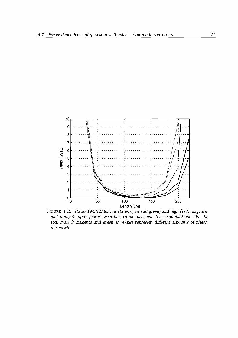
4.7. Power dependence of quantum well polarization mode converters 55
••• "0 •••••••••••• '0 ••••••••••• "0 •••••••••· . .
· . .........................................· . .
· . .• ................ ••0 •••••••••••• ,0 •••••••••••
10 ,...-----.r:,-........,,...----........,r-------.,r----"""'""II'''T''""--,
9 .
8 .
7 .
UJt:~f-.Qiii0:::
6 - .
5 .
4 , .
3 ..
2
1
o'--__--L ~ !iiiii=:~~::::::::::.____.i_J
o 50 100 150 200Length [~m]
FIGURE 4.12: Ratio TM/TE for low (blue, cyan and green) and high (red, magentaand orange) input power according to simulations. The combinations blue &red, cyan & magenta and green & orange represent different amounts of phasemismatch
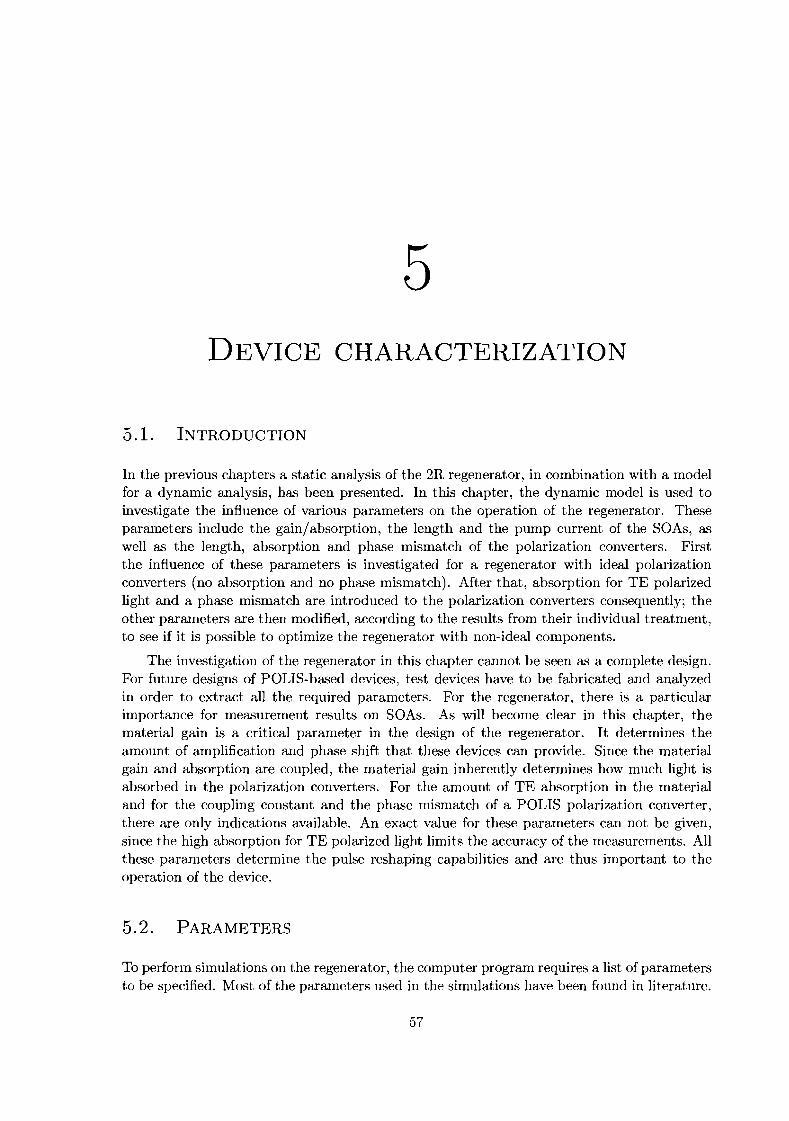
5DEVICE CHARACTERIZATION
5.1. INTRODUCTION
In the previous chapters a static analysis of the 2R regenerator, in combination with a modelfor a dynamic analysis, has been presented. In this chapter, the dynamic model is used toinvestigate the influence of various parameters on the operation of the regenerator. Theseparameters include the gain/absorption, the length and the pump current of the SOAs, aswell as the length, absorption and phase mismatch of the polarization converters. Firstthe influence of these parameters is investigated for a regenerator with ideal polarizationconverters (no absorption and no phase mismatch). After that, absorption for TE polarizedlight and a phase mismatch are introduced to the polarization converters consequently; theother parameters are then modified, according to the results from their individual treatment,to see if it is possible to optimize the regenerator with non-ideal components.
The investigation of the regenerator in this chapter cannot be seen as a complete design.For future designs of POLIS-based devices, test devices have to be fabricated and analyzedin order to extract all the required parameters. For the regenerator, there is a particularimportance for measurement results on SOAs. As will become clear in this chapter, thematerial gain is a critical parameter in the design of the regenerator. It determines theamount of amplification and phase shift that these devices can provide. Since the materialgain and absorption are coupled, the material gain inherently determines how much light isabsorbed in the polarization converters. For the amount of TE absorption in the materialand for the coupling constant and the phase mismatch of a POLIS polarization converter,there are only indications available. An exact value for these parameters can not be given,since the high absorption for TE polarized light limits the accuracy of the measurements. Allthese parameters determine the pulse reshaping capabilities and are thus important to theoperation of the device.
5.2. PARAMETERS
To perform simulations on the regenerator, the computer program requires a list of parameterst.o be specified. Most of t.he paramet.ers used in the simulat.ions have been found in lit.erat.ure.
57

58 Chapter 5. Device characterization
Polarization dependent parameters are included twice in the simulation software, once foreach polarization. All were chosen conservatively, so that in reality any deviation from thesevalues will turn out beneficial.
First an overview is given of all parameters that are related to the geometry of the devicesused in the regenerator; these are listed in table 5.1. The length of the full polarizationconverter was chosen to match the optimum converter length determined from the devicesfabricated by U. Khalique ([17]). The length of the partial polarization converters has beenderived from that length, as was the coupling constant in chapter 4. The length of the SOAshas been chosen to be 1 mm, according to simulation results presented in the next section.
Device: Parameter: Value: Source:Polarization converter Length (partial) 3211m
Length (full) 123 pm [17JWidth active region 0.85 11m [32,33JDepth active region 3.0 nm [32,33JCoupling strength 12724.77.10-6 llm- 1 Section 4.3Phase mismatch 4000.10-6 llm- 1 [32J
SOA Length 1.0 mm Section 5.3Width active region 3.0 11m [32,33JDepth active region 3.0 nm [32,33J
Common r 0.005 [30JrKerr 0.4 [20J
TABLE 5.1: Geometry related parameters
Table 5.2 gives an overview of the values of known parameters, related to the POLISmaterial.
Parameter: Value: Source:Effective refractive index 3.4 [32,33JWavelength 1550 nm [32,33JTM absorption 600 dBm- 1 [32,33JTE absorption 18000 dBm-1 [32,33J
TABLE 5.2: POLIS related parameters
Table 5.3 lists the remaining parameters. Many of these parameters concern the dynamicbehavior of the SOAs. Later in this chapter it will become clear that these parameters havea big influence on the operation of the regenerator. Exact values, however, are not required,since their combined effect is self explanatory.
5.3. SIMULATIONS
With the approximate values that have been collected for the parameters participating in themodel, the influence of variations in design parameters can be investigated. The design parameters to be considered in this chapter are: the gain, length and pumping current of the SOAs,

5.3. Simulations
Device: Parameter: Value: Source:SOA Material gain 2350 m ·1 [12, 21, 23, 26]
Tr. carrier density 1.5 . 1024 m-3 [27]A 0.3 . 10-9 s-1 [6]B 1.0. 10-16 m3s-1 [6]C 1.0. 10-40 m6s-1 [6,22]1"1 0.2 W-l [20]aN 5 [28JPassive losses SOA 6.0.102 dBm-l [32]Free carrier abs. 5.0 . 10-22 m2 [20JNL refr. index -3.5 . 10-16 m2W-l [20]
TABLE 5.3: Material related parameters
59
the length of the polarization converters, the presence of absorption and phase mismatch inthe polarization converters and the number of quantum wells. The effect of variations in thefirst four parameters is studied individually, assuming ideal polarization converters. Later,absorption and a phase mismatch in the polarization converters are introduced consequentlyand an attempt is made to correct for their effects by using the results obtained from the firstsimulations.
The simulations performed to investigate the effect of variations in the design parametersare carried out with Gaussian pulses. These pulses have an FWHM of 2.05 ps and a floorlevel of 1 . 10-18 Watt (to p~event numerical errors). Other pulse shapes and widths havebeen used to investigate the reshaping capabilities of the regenerator, their use is mentionedspecifically.
SOA LENGTH AND GAIN
The analysis of the regenerator is started from the most simple situation. The polarizationconverters are assumed to be ideal and the lengths of the partial polarization converters issuch that their splitting results in 75% TM and 25% TE. A parameter still to be determinedis the length of the SOAs. For this, the material gain is assumed to be 2350 m-l and the SOAinjection current is assumed to be 200 rnA, corresponding to a carrier density of 1 .1025m-3
in equilibrium. The requirement for the SOAs is to be able to provide enough phase shift fora certain pulse energy, so that switching by means of this phase shift is possible.
The decision was made to calculate the length of the SOAs such that the regeneratorwould be completely "transparent" for a power level of 100 mW. The length of the SOAs iscalculated with the self phase modulation model presented in appendix B. The script used forthese calculations is presented in appendix G. The script calculates the difference in phaseshift that both fractions of the pulse (75% and 25% of the input energy) obtain when passingthrough the individual SOAs. A Gaussian pulse, as mentioned above, with a peak power of100 mW contains an energy of 0.22156 pJ.
Figure 5.1 shows the output of the MATLAB script. In this figure the phase shift ofthis pulse is plotted as a function of the length of both SOAs through which both fractionsof the pulse travel. The blue line indicates the case in which the SOA gain is 100 dB/ cm

60 Chapter 5. Device characterization
(2350 m- I ), the red and green line correspond to gain values of 120 dB/cm and 80 dB/cmrespectively.
-0.5 .
_ -1
~~~ -1.5 ~ ..
j0.. -2 ...
-2.5 .
-3L...- .o....- ""'---- ...J
o 500 1000 1500SOA Length [lun]
FIGURE 5.1: Phase shift as a function of SOA length for different values of SOAgain
The regenerator is transparent if the phase difference between the light in the regeneratoris equal to 7r/2 radians, the light is then completely transferred from TM at the input to TMat the output. From the results presented in figure 5.1 it follows that the length of both SOAshas to be less than 1 mm. To keep a safe margin, the length is chosen to be 1 mm, keeping inmind that the values found with the self phase modulation model are not exact values sincelosses were neglected.
The next parameters to be investigated are the material gain, the length of the SOAsand the injection current of the SOAs. All are varied to three different values. The length isvaried from 500 pm, 750 pm and 1000 11m. The material gain is chosen to be 80 dB/cm, 100dB/cm and 120 dB/cm. And for the injection current the values of 50 rnA, 200 rnA and 800rnA are investigated. The results from these simulations are presented in the figures 5.2(a)to 5.4(b).
10 r;==~!!::::::=""l":'::::::::::::::::::;~--::::::::J--BOdB/em
o -"--- 100 dB/em--120dB/em
-10
iii -20 .. '.' ..........•.•
:E..~ -30 ....... '.' ~ .....,en
::;;f- -40
-50
-60
-70 ""--__"'---__""'---__.......~_-'-__.....J
10'5 10'" 10'3 10-2 10-' 10·
Input pulse energy [pJ]
o .
-1 . . .
-2 .
iii -3 .. '.' ..... ".".. '.' '." .... , .....:E..~ -4 .(!)
~ -5 .. '.' ..... u • .-• ...............
-6 ---- .
-7 " .•.•.•- ..
10-3 10-2
Input pulse energy [pJ]
-,10
(a) (b)FIGURE 5.2: Transfer curve of the 2R regenerator as a function of pulse energy for
various values of material gain. Length is 1 mm and current is 200 mA
From figures 5.2(a) and 5.2(b) it becomes clear that the operation of the regenerator is

5.3. Simulations 61
strongly dependent on the amount of gain available in the SOAs. A higher gain in both SOAsresults in saturation at smaller energies and vice versa. This can be understood when takinginto account that the saturation energy of a SOA is equal to equation 5.1. For the transfercurve of the regenerator, a higher material gain results in a shift towards lower energies aswell as in an increase in the total device gain.
(5.1)
The transfer curves of the regenerator for different lengths of the regenerator are presentedin figures 5.3(a) and 5.3(b). As can be seen from this figure the results are quite similar tothe results for variations in the material gain. Shorter SOAs result in less phase shift and alower amplification of the light. The transfer curve of the regenerator therefore shifts towardslower energy levels for longer SOAs.
-16 .
-18 .
. . .... ... . -:. -:. : :: ::.::::.. -:. -:. ~ .: ~ ::::::
-20 ---- - .
-22 L..-__.......___'___........__--'-_.;;:::"..--'
10" 10" 10.3 10'2 10" 10°
Input pulse energy [pJ)
.~ -12 . .: ...:.. :.::.:.,.:..•• <.._>+,.;.:,;:.••.. :.-:'"~.;; ::.::..._~ .• :,.~:::; :::.Cl~ -14 ..... , ... ~ ...•.•.
-8 .
iii -10:Eo
-80 L..- .......__-'-__........__--'-__--'
10" 10'3 10'2 10" 10°
InplIl pulse energy [pJ]
--500~m
o _ ...._. 750~
-10 --1000~ ::;::;:
-20 .
-70 .
-50
-60
iii:Eo -30 .c:'0;
Cl -40 """'" .
~
(a) (b)FIGURE 5.3: Transfer curve of the 2R regenerator as a function of pulse energy for
various values of SOA length. Gain is 100 dB/cm and current is 200 mA
Figures 5.4(a) and 5.4(b) show the results for simulations performed at different levelsof injection current. Again the results are comparable to the results of the first two testsperformed on the regenerator. From this it can be concluded that if, after measurements,it turns out that the gain of a SOA, fabricated in POLIS material, is lower than expected,the feasibility of a 2R regenerator according to the presented concept is not compromised.However, it is not possible to tune the total device amplification and the point of maximum"transparency" independently of each other.
In this section it was shown that the concept device does indeed have the non-lineartransfer curve that was predicted. The amount of amplification of the SOAs has a largeinfluence on the operation of the regenerator. This can be seen from the position and shapeof the transfer curve. The amount of amplification can be influenced by changing either thelength or the pump current of the SOAs.
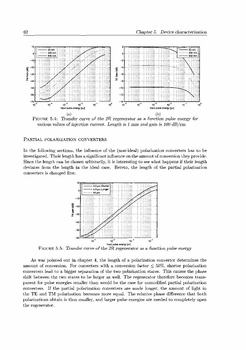
62 Chapter 5. Device characterization
.,10
::~:<~ ~~·~j·~T.••..•. _ 0 ••0- . ':' ,;': ::~:::.. ':.~: ::::::, .. ~.:::~:
.............. -- .
-6 .
. . .. _-.--14 '--__.......__~__~ "'______..J
10.5 10.... 10'3 10.2
Input pulse energy [pJ]
o
-2
-12 .
-10 -
in -4:E..~
c3w>- -8
-70L.----'-----~--~---~-~...10'5 10.... 10.3 10.2 10" 10°
Input pulse energy [pJ]
-50
-60
in -20 .:E.
.~ -30Cl::>>- -40
(a) (b)FIGURE 5.4: Transfer curve of the 2R regenerator as a function pulse energy for
various values of injection current. Length is 1 mm and gain is 100 dB/em
PARTIAL POLARIZATION CONVERTERS
In the following sections, the influence of the (non-ideal) polarization converters has to beinvestigated. Their length has a significant influence on the amount of conversion they provide.Since the length can be chosen arbitrarily, it is interesting to see what happens if their lengthdeviates from the length in the ideal case. Hereto, the length of the partial polarizationconverters is changed first.
-40
-50
-10
--4.5 ~m Shorter :::
o -- 4.5 ~m Longer :::40~m
10.... 10'3 10.2 10"
Input pulse energy [pJ]
FIGURE 5.5: Transfer curve of the 2R regenerator as a function pulse energy
As was pointed out in chapter 4, the length of a polarization converter determines theamount of conversion. For converters with a conversion factor ~ 50%, shorter polarizationconverters lead to a bigger separation of the two polarization states. This causes the phaseshift between the two states to be larger as well. The regenerator therefore becomes transparent for pulse energies smaller than would be the case for unmodified partial polarizationconverters. If the partial polarization converters are made longer, the amount of light inthe TE and TM polarization becomes more equal. The relative phase difference that bothpolarizations obtain is thus smaller, and larger pulse energies are needed to completely openthe regenerator.

5.3. Simulations 63
.. ,,',.- --.-'-
~f: :::::::.. ,: - .. :/::: .. - - ....
10'3 10'2
Input pulse energy [pJ]
. '." '.' ~ .".~... . ..' '.' " .. ~ ~" . " .. . . ' .
10-.4
o ...:- :.:.:.:.:,:: ...:..:., ----.
:::;~.. ':g:'":,:;::'"':;='~----~:.: (:::::" .'.:''-':''
. ·f······-4 .............•.,.. " ..... " •.'.,.'
-8 ---- .
-6 .
c:
~ -2
iii 2 ..
:!2.
-10'-------~--~-- ......--'---"'---.........10'5 10-.4 10'3 10'2 10" 10°
Input pulse energy [pJ]
-6 .
-8 ........•.•... '''''--' _.••.
-4 .... '.'.'.'.'.•.• '
iii 2··········
:!2.cO·········· .'iiiCl
(a) (b)FIGURE 5.6: Transfer curves of the 2R regenerator for partial polarization convert-
ers of unequal length: shorter-longer (a) and longer-shorter (b). The line "TMOriginal" represents tlle unmodified situation
The lengths of both partial polarization converters can be varied independently of eachother. The effect of having two partial polarization converters of unequal length is shown infigures 5.6(a) and 5.6(b). In the first case, the first partial polarization converter is shorter(5·2.204 pm) and the second converter is longer (5·2.204 pm) as compared to the originalca..<;e (equal lengths, see figures 5.2(a) to 5.4(b)). The result is a floor-level. which extendsover a fairly long range of pulse energies. The transition to a net gain bigger than zero occursearlier than for the original situation and the maximum amount of gain is bigger.
The floor-level is caused by the last partial polarization converter, which in this case istoo long. The conversion to TE is therefore incomplete. The result of the higher net gainof the converter is caused by the shorter converters at the beginning of the regenerator. Ashorter converter leads to more splitting and saturation at lower energies.
In the second situation, the converter at the beginning is longer and the converter atthe end is shorter. The floor-level is again caused by the last polarization converter. Theconverter is too short and conversion to the TE polarization is, again, incomplete. The lowernet gain can be explained by the longer converter at the beginning. There is less splittingand less light is able to pass the regenerator.
From the analysis of the partial polarization converters, it can be seen that the smaller theconversion fraction, the lower the pulse energies are for which the regenerator is transparent.By choosing the lengths of the partial polarization converters unequal, the steepness of thetransfer curve can be controlled. The partial polarization converters allow us to fine tune theregenerator for a particular situation. This can be very useful in a ·future design, if losses andother negative influences inhibit proper behavior of the regenerator.
FULL POLARIZATION CONVERTER
Another important parameter with which undesired behavior of the regenerator can be corrected is the length of the full polarization converter. The influence of variations in its lengthis shown in figures 5.7(a) and 5.7(b). In these simulations, the length was either increased or
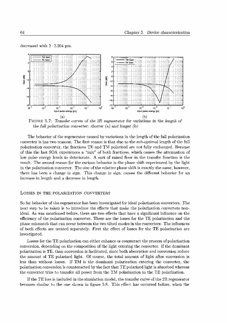
64
decreased with 2 . 2.204 pm.
4 r;::::::'=~~:::;-:-:-~---:-~":':":!'"""~~~-:--:-~...
I-TMGainl: :::::--TEGaln .
2 .. '.' ...•••.. - ' .
o ···..._·O"M_
. --- .. . .-4
-6 ' .
-8 L-__""'---__....... '--__.......__.....
10~ 10~ 10~ 10~ 10~ 1~
Inpul pulse energy [pJ]
Chapter 5. Device characterization
2
iii 0:E.c -2'iii(!) -4
-6 ...: ..:-:.:.:.:,:, ...:..:.: ::.:.::.:
-8 ' ,., ..- ,- -.
-10 .. ": .:.::.:::: ...:..:.:: ::::: .. .-12 L- ......__--' "'--__...J
10.5 10" 10'3 10'2 10" 10°
Inpul pulse energy [pJ]
(a) (b)FIGURE 5.7: Transfer curves of the 2R regenerator for variations in the length of
the full polarization converter: shorter (a) and longer (b)
The behavior of the regenerator caused by variations in the length of the full polarizationconverter is has two reasons. The first reason is that due to the sub-optimal length of the fullpolarization converter, the fractions TE and TM polarized are not fully exchanged. Becauseof this the last SOA experiences a "mix" of both fractions, which causes the attenuation oflow pulse energy levels to deteriorate. A sort of raised floor in the transfer function is theresult. The second reason for the curious behavior is the phase shift experienced by the lightin the polarization converter. The size ofthe relative phase shift is exactly the same, however,there has been a change in sign. This change in sign, causes the different behavior for anincrease in length and a decrease in length.
LOSSES IN THE POLARIZATION CONVERTERS
So far behavior of the regenerator has been investigated for ideal polarization converters. Thenext step to be taken is to introduce the effects that make the polarization converters nonideal. As was mentioned before, there are two effects that have a significant influence on theefficiency of the polarization converter. These are the losses for the TE polarization and thephase mismatch that can occur between the two tilted modes in the converters. The influencesof both effects are treated separately. First the effect of losses for the TE polarization areinvestigated.
Losses for the TE polarization can either enhance or counteract the process of polarizationconversion, depending on the composition of the light entering the converter. If the dominantpolarization is TE, than conversion is facilitated, since both absorption and conversion reducethe amount of TE polarized light. Of course, the total amount of light after conversion isless than without losses. If TM is the dominant polarization entering the converter, thepolarization conversion is counteracted by the fact that TE polarized light is absorbed whereasthe converter tries to transfer all power from the TM polarization to the TE polarization.
If the TE loss is included in the simulation model, the transfer curve of the 2R regeneratorbecomes similar to the one shown in figure 5.8. This effect has occurred before, when the
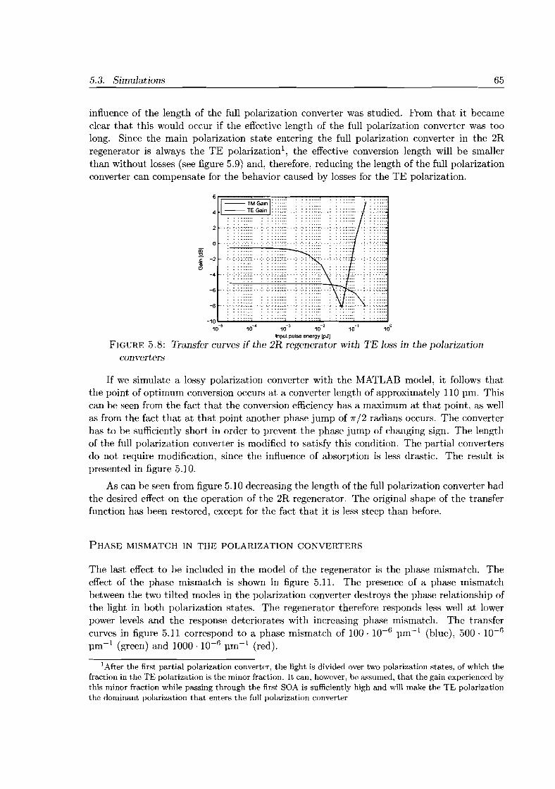
5.3. Simulations 65
influence of the length of the full polarization converter was studied. From that it becameclear that this would oceur if the effective length of the full polarization eonverter was toolong. Since the main polarization state entering the full polarization converter in the 2Rregenerator is always the TE polarization1, the effective conversion length will be smallerthan without losses (see figure 5.9) and, therefore, reducing the length of the full polarizationconverter can compensate for the behavior caused by losses for the TE polarization.
oiii':Eoc -2············'iiiCl
-4 .
-6 . ".' ·.·.·u.•.• . '.' ... " •.__."
-8 ..•.•...•.......
-1~O~-5:----1...0..---10....-3:----1...0"":"-2---1...0--,~-""100
Input pulse energy [pJ]
FIGURE 5.8: Transfer curves if the 2R regenerator with TE loss in the polarizationconverters
If we simulate a lossy polarization converter with the MATLAB model, it follows thatthe point of optimum conversion occurs at a converter length of approximately 110 11m. Thiscan be seen from the fact that the conversion efficiency has a maximum at that point, as wellas from the fact that at that point another phase jump of 1r/2 radians occurs. The converterhas to be sufficiently short in order to prevent the phase jump of changing sign. The lengthof the full polarization converter is modified to satisfy this condition. The partial convertersdo not require modification, since the influence of absorption is less drastic. The result ispresented in figure 5.10.
As can be seen from figure 5.10 decreasing the length of the full polarization converter hadthe desired effect on the operation of the 2R regenerator. The original shape of the transferfunction has been restored, except for the fact that it is less steep than before.
PHASE MISMATCH IN THE POLARIZATION CONVERTERS
The last effect to be included in the model of the regenerator is the phase mismatch. Theeffect of the phase mismatch is shown in figure 5.11. The presence of a phase mismatchbetween the two tilted modes in the polarization converter destroys the phase relationship ofthe light in both polarization states. The regenerator therefore responds less well at lowerpower levels and the response deteriorates with increasing phase mismatch. The transfercurves in figure 5.11 correspond to a phase mismatch of 100· 10-6 11m-1 (blue), 500· 10-6
11m-1 (green) and 1000· 10-6 11m-1 (red).
I After the first partial polarization converter, the light is divided over two polarization states, of which thefraction in the TE polarization is the minor fraction. It can, however, be assumed, that the gain experienced bythis minor fraction while passing through the first SOA is sufficiently high and will make the TE polarizationthe dominant polarization that enters the full polarization converter
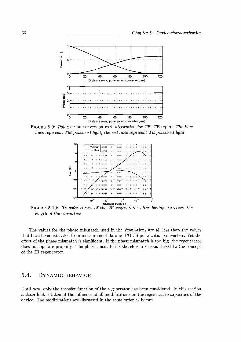
66 Chapter 5. Device characterization
12020 40 60 80 100Distance along polarization converter ~ml
OL-_=:i...-__........__.........__.......---.;=---.......,o
:::i~Q; 0.5
~a.
4r----...,....--~---r---...,....--~---T""1
. . . . . .'0 3 .: .: :- ~ ; ~
~ . . . . .j 2 1-'_'_'_._.'_'..;''-''-'-'-''-'-'-.;...._._.-''-'-'-''.;..''-'-'-''-'-'..;'',-'-'-''-'-'-''-.;.'-'-''-'-t-''_'.;.;"
a. 1
120
OL.-__-'-__---I. .L.-__-'-__---I._---L_.......
o 20 40 60 80 100Distance along polarization converter ~ml
FIGURE 5.9: Polarization conversion with absorption for TE, TE input. The bluelines represent TM polarized light, the red lines represent TE polarized light
o ,,- - .
-10
-15 .
· - - -.- .· .· .-20L.-~---_......-_ ---"'----....
10-4 10-3 10-2 10-' 10·
Input pulse energy [pJ]
FIGURE 5.10: Transfer curves of the 2R regenerator after having correctedlength of the converters
the
The values for the phase mismatch used in the simulations are all less than the valuesthat have been extracted from measurement data on POLIS polarization converters. Yet theeffect of the phase mismatch is significant. If the phase mismatch is too big, the regeneratordoes not operate properly. The phase mismatch is therefore a serious threat to the conceptof the 2R regenerator.
5.4. DYNAMIC BEHAVIOR
Until now, only the transfer function of the regenerator has been considered. In this sectiona closer look is taken at the influence of all modifications on the regenerative capacities of thedevice. The modifications are discussed in the same order as before.

5.4. Dynamic behavior 67
10rr====""",,='i'~~~-:-~. ":":...:!"".--:-~':":":':J--100.10""" ~m-1 :
500.1 0""" ~m-1 :--100.10-5~m-':· .
o _, -.-.-" _ ---
.. - .
. . .
-10
-15
10--<0
(a)FIGURE 5.11: Transfer curves of the 2R regenerator for various amounts of phase
mismatch
SOA LENGTH AND GAIN
First the regenerative capacities of the ideal regenerator are studied for single pulses, laterin this section regeneration of multiple pulses is considered. The pulses shown in the variousfigures in this section, are the same that were used to generate the transfer curves in theprevious section, unless specified otherwise. Figure 5.12 shows the response of the regeneratorwith ideal polarization converters on single Gaussian pulses, that contain different amountsof pulse energy. The pulses are plot on a logarithmic y-axis to facilitate comparison of theindividual pulses. The figure shows that the device concept does not only have the expectedtransfer function, but that it provides pulse width reduction and amplification as well. In thefollowing sections, the effect of the regenerator is always given by two figures, one in whichthe power is normalized, to clarify the effect on the pulse shape, and one with a logarithmicscale, to clarify the amplification.
--2.2-10-' pJ
--2.2.10-2 pJ~•._~ 2.2.10-3 pJ .
2.2-10-' pJ
--2.2·10-5 pJ .
10-12 L- .i......<"""-'_..L....i..-.....::.~_..i..-:::::=====I
-10 -5 0 10Relative time [ps]
FIGURE 5.12: Pulse reshaping and amplification for increasing pulse energy
-B10
-1.10 .
In figure 5.13(a) the response of the regenerator is shown for gain values of 80 dB/cm,100 dB/cm and 120 dB/cm respectively. In the plot power has been normalized, the FWHMtime of the incoming pulse is 8.3 ps. The pulse width reduction for the different gain valuesis 2.075 ps, 1.875 ps and 1.675 ps respectively. The reduction of the pulse width is dependent

68 Chapter 5. Device characterization
on the amount of gain and low gain provides better results than high gain. For higher gain,the transfer curve of the regenerator shifts towards lower energies and a bigger part of thepulse is able to pass the regenerator. For low gain, however, there is less amplification of thepulses.
1510oRelative time [ps]
-5-10
10° .--------,----.-----.---.........--...,....----,
10-6--120dB/em
100 dB/em--80 dB/em- - - Input pulse
10-8 L....L.f....l__......i..__.....i...__~==;i;;;;~~
-151510-10 -5 0Relative time [psI
I. .,.(
I.-j-
: I: I.I.i
............... ,:..I :
........ ·i .
.. ./ ./.
: ....oL-_.....'--_::o.!Il=---_---L__--'-__-=__...J
-15
0.2 ...
0.7
0.3
0.8
0.9 ...
0.1
;- 0.6~I;; 0.5
~0.. 0.4
(a) (b)FIGURE 5.13: Pulse shortening for variations in material gain
The same is valid for variations in the length and injection current of the SOAs. Theresults of these simulations are shown in figure 5.14(30) to 5.15(b). Longer SOAs or a higherinjection current lead to a bigger phase shift and to saturation at low pulse energies. Gainand phase shift are related, therefore longer SOAs and high current lead to more amplificationas well.
15105
/~ .,;
,;:/.
/./.:
//
/
10° .--------.-----,.----.---~---r--____,
--1mm
75O~m
--500~m
- - - Input pulse10-8 L_Lt...L_......i..__.....i...__....J:::==:i:::::::::::::::::..J
-151510
--1mm••" ••.•.•• 750 ~m
--500~m
- - - Input pulse
-10 -5 0Relative time [ps]
: ....ol..-_.....::>__""""=---_--'-__--'-__-=__...J
-15
0.8
0.9
0.7
0.2
0.1
0.3
/ :.. I·
I... .,.
......... ,J.I
~0.6/
~ 0.5 : J
0.. 0.4 : i.i
........ 1'
I :........ i'
.J./.
(a) (b)FIGURE 5.14: Pulse shortening for variations in SOA length
PARTIAL POLARIZATION CONVERTERS
Changes in the lengths of the partial polarization converters have also been investigated. Theeffect of increasing or decreasing the length of both partial polarization converters on thepulse reshaping is quite obvious. A reduction in length of the partial polarization converters
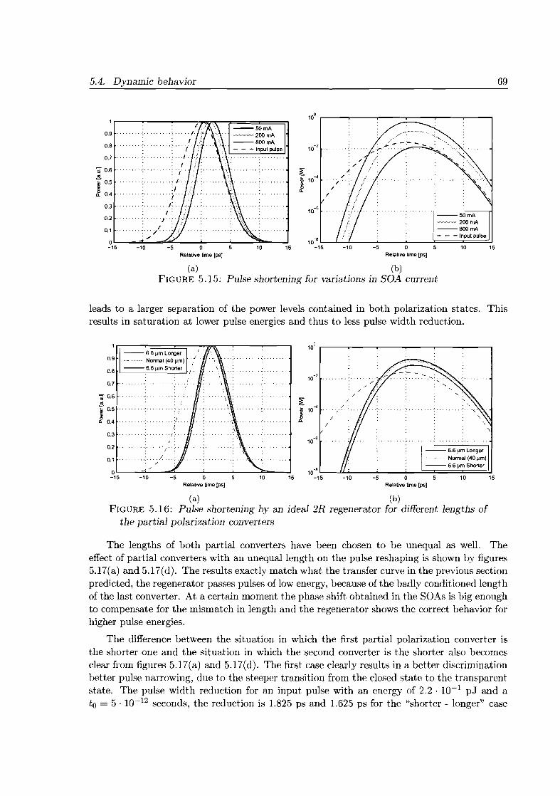
5.4. Dynamic behavior 69
0.2
0.1
15o 10Relative time [ps]
-5-10
/.'F
//
10° .-----.....,..--...,.---.,....-----,----r--..,
--50mA-_.•- 200mA--600mA- - - Input pulse
10-8L..LU__....i....__-'---_----l==;:::i;:::::::::=~
-15
I... ,.
I.,. .
.~ .. ./ .: I
. . ': . I.:..f. ..
: I····r
0.3 ".r ..I .
...,"". I ....:... / .....:",
0.8
0.9 .
~1'::-5----::Ll0--'""-5~----'0--~5---"10'""""-......15
Relative time Ips]
0.7 .
-; 0.6 ..
~lD 0.5
~ 0.4
(~ (b)FIGURE 5.15: Pulse shortening for variations in SOA current
leads to a larger separation of the power levels contained in both polarization states. Thisresults in saturation at lower pulse energies and thus to less pulse width reduction.
1510
--6.6 11m Longer
Normal (40 11m)
-- 6.6 11m Shorter
-5 0Relative time [ps]
10°
-210
~ ....
.... /
[ /.
lD 10'" '/~ /............. .l1.
/
-810
-810
10 15 -15 -10-5 0Relative time [psI
-10
......: i
--6.6 11m Longer
Nonnal (40 11m) .__ 6.6llffi Shorter I
. .'/ .
0'------""---""'----'----'-------'==--......-15
0.2 .
!0.3 .. . /:.
0.1
0.7
-; 0.6
~lD 0.5~<L 0.4
(a) (b)FIGURE 5.16: Pulse shortening by an ideal 2R regenerator for different lengths of
the partial polarization converters
The lengths of both partial converters have been chosen to be unequal as well. Theeffect of partial converters with an unequal length on the pulse reshaping is shown by figures5.17(a) and 5.17(d). The results exactly match what the transfer curve in the previous sectionpredicted, the regenerator passes pulses of low energy, because of the badly conditioned lengthof the last converter. At a certain moment the phase shift obtained in the SOAs is big enoughto compensate for the mismatch in length and the regenerator shows the correct behavior forhigher pulse energies.
The difference between the situation in which the first partial polarization converter isthe shorter one and the situation in which the second converter is the shorter also becomesclear from figures 5.17(a) and 5.17(d). The first case clearly results in a better discriminationbetter pulse narrowing, due to the steeper transition from the closed state to the transparentstate. The pulse width reduction for an input pulse with an energy of 2.2 . 10-1 pJ and ato = 5· 10-12 seconds, the reduction is 1.825 ps and 1.625 ps for the "shorter - longer" case

70 Chapter 5. Device characterization
10°
0.9
0.8 10-2
0.7
-; 0.6 [~ iii 10'"jj; 0.5
~~0 Q. --2.2·10-' pJQ. 0.4
-- 1.1.10-1 pJ0.3 4.4.10-2 pJ .
0.2 2.2.10-2 pJ
0.1 . ~ .. 2.2.10-3 pJ
--2.2·10'" pJ0 10-8
-15 -10 -5 0 5 10 15 -15 -10 -5 0 5 10 15Relative time [ps] Relative time [ps]
(a) (b)
10°
0.9-- 2.2 10-' pJ
-- 1.1.10-' pJ
0.8 4.4.10-2 pJ
_._. 2.2·10'2 pJ-2
100.7 ..............
2.2.10-3 pJ
-; 0.6 -- 2.2·10'" pJ[~
iii 0.5 iii 10'"
~ ~Q. 0.4 Q. --2.2·10" pJ
0.3-- 1.1.10-' pJ
4.4·10'2 pJ
0.2 2.2.10-2 pJ .
0.1. 2.2.10-3 pJ
10-8--2.2·10" pJ
0-15 -10 -5 0 10 15 -15 -10 -5 0 5 10 15
Relative time [ps) Relative time [PS)
(c) (d)FIGURE 5.17: Pulse shortening by an ideal 2R regenerator with unequal partial
polarization converters (a) & (b) 4.4 pm shorter - 4.4 pm longer, (c) & (d) 4.4 pmlonger - 4.4 pm shorter
and the "longer - shorter" case, respectively.
Changing the length of the partial polarization converters enables fine tuning of theregenerator. The amount of pulse narrowing and the discrimination of the energy levels caneither be increased or decreased, but are dependent on each other. The changes in length ofthe partial converters required to achieve the desired behavior are very small. The concept istherefore very sensitive to this parameter.
FULL POLARIZATION CONVERTERS
The previous paragraph already made clear that the modifications made to the length of thefull polarization converter are more critical. If the length of the full polarization converter isincreased above the optimum conversion length, the phase difference between the TE and TMpolarization switches signs. This causes the regenerator to be open from the beginning. Thesituation is more complicated if absorption is also included in the converters. The optimumconversion length then becomes power dependent. This can be compensated for by decreasing

5.4. Dynamic behavior 71
the length of the full polarization converter sufficiently.
Figures 5.18(a) and 5.18(b) show the effect of changes in length on the reshaping capabilities of the regenerator. For a decrease in length the only effect is that the regenerator istransparent for small pulse energies. In figure 5.18(a), this can be seen from the fact thatthose pulses are not narrowed. Normal behavior of the regenerator is found at larger pulseenergies (~ 2.2· 10-2 pJ).
1510
--2.2.10. ' pJ
--1.1.10-1 pJ
4.410-2 pJ
2.210.2 pJ
2.2.10-3 pJ
. --2.2·10.... pJ
-5 0 5Relative lime [psI
0.9
O.B ..
0.7
,; 0.6~
I 0.5
"- 04
0.3
0.2 ..
0.1
015 -15 -1010
--2.2.10.' pJ
-- 1.1.10.' pJ. _._.~••. 4.4.10.2 pJ
2.2.10.2 pJ
2.2.10.3 pJ
--2.2.10.4 pJ
-5 0 5Relative time [psI
-10
0.3
0.7 .
O.B .
0.1
0.9 .
0.2
;- 0.6 ..
~iii 0.5
~"- 0.4 ..
(a) (b)FIGURE 5.18: Pulse shortening by an ideal 2R regenerator for a shorter (a) and a
longer (b) full polarization converter
As the figure shows, a too large length of the full polarization converter results in undesiredbehavior. Because the phase difference of the light changes sign if the polarization converteris even slightly longer than the optimum conversion length, the behavior of the regeneratorchanges drastically. Again, pulses with a small pulse energy can pass freely. At intermediateand larger amounts of pulse energy, the regenerative process becomes visible. First the trailingpart of the pulse is blocked and if the energy increa..<;es even further, the part of the pulsethat is blocked shifts, through the pulse from back to front. For certain pulse energies, the"reshaped" pulse is split up in two smaller pulses.
This is behavior was predicted by the transfer curve of the regenerator. The transfercurve (5.7(b)) showed a valley for pulse energies around 2.2.10-2 pJ. Such behavior is notacceptable in a regenerative device and therefore attention has to be paid when determiningthe length of the full polarization converter.
LOSSES IN THE POLARIZATION CONVERTERS
Figures 5.19(a) and 5.19(b) show the effect of the presence of absorption in the polarizationconverters on the output of the regenerator. The amount of absorption is 180 dB/cm for theTE polarization. It can be seen that the regenerator is transparent for pulses that containvery little energy, there is no reshaping visible. For higher pulse energies, the pulses startto break up. The position of where the pulses break, is dependent on the total energy theycontain. For the highest pulse energies used in the simulations, the behavior of the regeneratorlooks more and more like that of a regenerator without the losses for TE polarized light
The next two figures (figures 5.20(a) and 5.20(b)) show the response of the regenerator
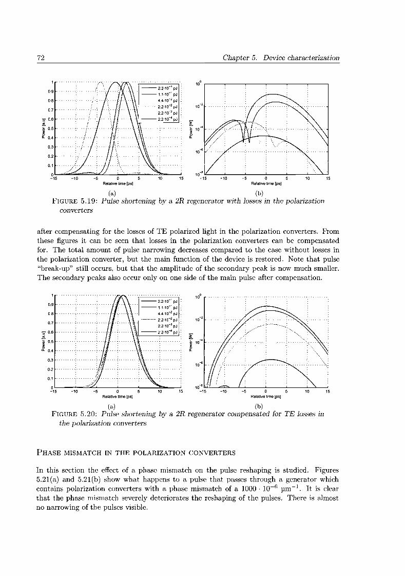
72 Chapter 5. Device characterization
1510-5 0Relative time [psI
-10
10° r--~--~--~-~~----'---...,
1510
--2.2·10·' pJ
-- 1.1.10·' pJ .
4.4.10.2 pJ .
2.2.10.2 pJ
2.2.10.3 pJ .
-- 2.2.10.4 pJ .
-5 0Relative time [psl
0.9
0.8
0.7
'5' 0.6.!2.~ 0.5~
D.. 0.4
0.3
0.2
0.1
0-15 -10
w (~FIGURE 5.19: Pulse shortening by a 2R regenerator with losses in the polarization
converters
after compensating for the losses of TE polarized light in the polarization converters. Fromthese figures it can be seen that losses in the polarization converters can be compensatedfor. The total amount of pulse narrowing decreases compared to the case without losses inthe polarization converter, but the main function of the device is restored. Note that pulse"break-up" still occurs, but that the amplitude of the secondary peak is now much smaller.The secondary peaks also occur only on one side of the main pulse after compensation.
1510-5 0Relative time (ps]
-10
10'"
1510
--2.2·10·' pJ :.. --1.1·10·' pJ ':
4.410.2 pJ .:
--_.•... 2.2.10.2 pJ :
2.2.10.3 pJ .
. -- 2.2·10-4 pJ .:
-5 0Relative time [ps]
-10
oL...- ~=::.......__.........__"'--_......;J____'
-15
0.3
0.2
0.7 ,.
0.1
0.8 .
0.9
'5' 0.6.!2.~ 0.5~
D.. 0.4
(~ (b)FIGURE 5.20: Pulse shortening by a 2R regenerator compensated for TE losses in
the polarization converters
PHASE MISMATCH IN THE POLARIZATION CONVERTERS
In this section the effect of a phase mismatch on the pulse reshaping is studied. Figures5.21(a) and 5.21(b) show what happens to a pulse that passes through a generator whichcontains polarization converters with a phase mismatch of a 1000 . 10-6 pm-1. It is clearthat the phase mismatch severely deteriorates the reshaping of the pulses. There is almostno narrowing of the pulses visible.

5.4. Dynamic behavior 73
oL...-_""""'''''''-_-'----__'--_-'-__..::J::Io_--'
-15 -10 -5 0 5 10 15Relative lime [psl
0.9 .
0.8 .
0.7 .
;- 0.6 .
~.. 0.5 .
~Q. 0.4 .
0.3 .
0.2 .
0.1
.................
--2.2·10-' pJ
. -- 1.1·10-' pJ .
4.4.10-2 pJ .
2.2.10-2 pJ
2.2·10-' pJ .
. --2.210-4 pJ ·
-10 -5 0 5Relative time Ips]
10 15
(a) (b)FIGURE 5.21: Pulse shortening by a 2R regenerator with a phase mismatch in the
polarization converters
The value for the phase mismatch used in the simulations is approximately 4 times smallerthan the value determined from measurements. It is therefore likely that in reality realizationof the 2R regenerator concept is difficult. The results of the phase mismatch can not becompensated for, since the process influences the amplitude of the polarizations as well as thephase difference between them.
PULSE NARROWING
To study the pulse narrowing capabilities of the regenerator, simulations have been carried outon Gaussian pulses that contain an equal amount of energy, but that have a different FWHM(to) and thus a different peak power. This way it can be investigated if the regeneratorresponds to the amount of energy that has passed the device rather than the instantaneouspower levels of the input signal. The result of this test is shown in figure 5.22. The plot showsa linear increase of the pulse narrowing as a function of the pulse width. From this can beconcluded that the regenerator operates on an energy basis. The broader the pulse (largerto), the less energy it contains in the time interval t = -00 to t = T (see equation B.9). Ittherefore takes longer for the regenerator to become transparent if a wide pulse is applied atthe input and thus a larger part of this input pulse is blocked.
RESHAPING
In the following sections, the effect of the energy dependence on the reshaping, noise suppression and response time of the regenerator are investigated. To test the effect of the energydependence on the reshaping capabilities, the regenerator has been tested with a square pulse.Except for the transitions at the beginning and end of the pulse, a square pulse contains nofast transitions of low amplitude. Such a pulse should, ideally, remain unaffected by theregenerator. The response of the regenerator on a square pulse is given in figure 5.23.
The square shape of the input signal leads to a linear increase of power in time. The resultis the "sawt.ooth" shaped output, which is the combined effect of the increasing transparency

74 Chapter 5. Device characterization
4.5 .------,----.----r--~----.----.----.----r----,
4 .
3.5 .
~ 3cog 2.5 .
~.c: 2·
i.!!l 1.5 ..:::>
Q..
0.5 .
oL....-----L---'---'-----.L..-----'_........._ ........._ .........--I
1 4 5 6 7 6 9 10to [ps)
(a)FIGURE 5.22: Pulse shortening as a function ofta
0.25 r;::::=::::::::::::::::=::::;-----,----:-----.---I--TMOut-- Input pulse
0.2
~ 0.15
~Q.. 0.1
0.05 ..
oL....- L...oll.__----'~__....... ___J
-5 -2.5 0 2.5Relabve time [ps)
(a)FIGURE 5.23: Response of the regenerator on a square pulse
and the constant amplification of the pulse. From this can be concluded that the conceptregenerator is not suitable to operate as a shape-restoring device.
NOISE SUPPRESSION
Redistribution of the power density function of the noise around the zero and one levels ofan optical signal and increasing the extinction ratio are the most important functions of a 2Rregenerator. Figure 5.24 shows an optical pulse polluted with white noise and the response ofthe 2R regenerator on this optical pulse. The noise at the beginning of the pulse is successfullyremoved from the signal. The noise on the pulse itself and in the trailing part of the pulseis able to pass the regenerator. Noise containing transitions faster than the recovery time ofthe SOAs can not be removed by the regenerator.
REGENERATION OF MULTIPLE PULSES
The regeneration of an optical signal should be constant throughout time. In the previoussection it occurred that noise is only suppressed at the front of the pulses that are sent through
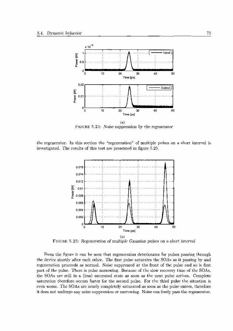
5.4. Dynamic behavior
f°JJAl:~'"P~jo 10 20 30 40 50
Time Ips)
f::J········I·········I·A'·2·:T~:jo 10 20 30 40 50
Time Ips)
(a)FIGURE 5.24: Noise suppression by the regenerator
75
the regenerator. In this section the "regeneration" of multiple pulses on a short interval isinvestigated. The results of this test are presented in figure 5.25.
0.016
0.014
.. ,', ,", : : .· . . .
· . . .......... '., ,,' .
· . . .......... '" '., , .
0.012
;[ 0.01
~ 0.008a..
••••••••• • "0 ••••••••• ,', ••••
· .
......... ,', ,", .· .
...................... .
. . . . .. . . . . . .. . . . ~ . . . .. .
0.006
0.004
0.002
10 20 30Time Ips)
40 50
(a)FIGURE 5.25: Regeneration of multiple Gaussian pulses on a short interval
From the figure it can be seen that regeneration deteriorates for pulses passing throughthe device shortly after each other. The first pulse saturates the SOAs as it passing by andregeneration proceeds as normal. Noise suppressed at the front of the pulse and so is firstpart of the pulse. There is pulse narrowing. Because of the slow recovery time of the SOAs,the SOAs are still in a (less) saturated state as soon as the next pulse arrives. Completesaturation therefore occurs faster for the second pulse. For the third pulse the situation iseven worse. The SOAs are nearly completely saturated as soon as the pulse enters, thereforeit does not undergo any noise suppression or narrowing. Noise can freely pass the regenerator.

76 Chapter 5. Device characterization
MODE-LOCKING
In chapter 2 it was explained that the regenerator could also be used in the application ofa mode-locked laser. In this section a closer look is taken on the mode-locking properties ofthe device. The simulations performed are those of a regenerator contained in a ring-shapedstructure, with an MMI to couple light in and out of the structure.
To start as simple as possible. The losses and phase mismatch have been left out of themodel. This way, the effect of the most basic behavior of the device concept on mode-lockingcan be investigated. The cavity is seeded with a single TM polarized pulse, described byequation B.8, containing an energy of 2.2156 . 10-1 pJ and having a to of 5 ps. The onlyvariable varied is the current.
Figures 5.26(a) and 5.26(b) show the behavior response of the device for a single inputpulse, while the SOAs are fed with an injection current of 346 mAo The input pulse is slowlynarrowed and amplified. The phase of the light is linearly increasing. The behavior looksstable, except for the fact that the pulse is damped after a couple of roudtrips.
250020001000 1500TIme [PSI
500
70
30
20 .
40 .
--TMPhase90 -- TE Phase
80 , ,.
100~====~""""'---'---~--:llJ'l
60 .
~III 50
J!!Q.
X 10-43.51--:----.T--~-r==::::::::====j]
.I-TMOuII
... --TEOu! I.
2.5
0.5
llh,','"0
0 500 1000 1500 2000 2500 0Time [PSI
[ 2
~Q. 1.5
(a) (b)FIGURE 5.26: Damped mode-locking after seeding an input pulse: power (a) and
phase (b)
To see if it is possible to achieve a situation in which the pulse amplitude stabilizes itself,the current was slightly increased to 347 mAo The response of the device after seeding thesame pulse as in the previous simulation, are given by figures 5.27(a) and 5.27(a).
As can be seen from these figures, the seeded pulse is reshaped and slowly amplifiedduring the first approximately 800 ps. After 800 ps, the phase behavior of the pulse becomesunstable. Changes in phase increase and what was first a linear increase in phase, nowbecomes a decrease. A closer look on the power plot learns us that the pulses start to breakup and that this process is unable to stop itself.
The boundary between a "stable" damped situation and an "unstable", longer lastingsituation is very small, concerning the current. This became clear from more simulations inwhich the current was varied on a sub-mA basis. This is most likely caused by the fact thatthere is no limiting element inside the cavity. For pulses with containing very little energy,the SOAs do not saturate and the carrier density distribution inside the SOAs remains thesame. If the current, and thus the gain, is low, the situation eventually damps out. If the
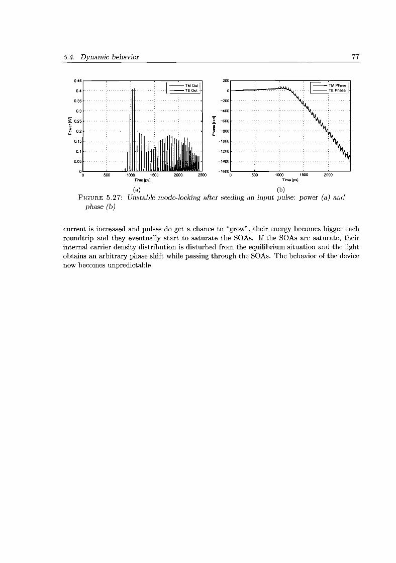
5.4. Dynamic behavior 77
2000
--TMPhase--TEPhase
1000 1500Time [ps}
500
200 ,----,---.......---.----;====~
-200
-400
'5'~ -600
"'".. -600&:Q.
-1000
-1200
-1400
-16002500 020001000 1500
Time [psl500
oL-__-'--_...1.lJil.J..llLJLLU........
o
0.1
0.4 ....................•.
0.3 .. . ,.
0.15 . .. , ..
0.05 .
0.35 .
0.45,--...,.....----,------,--""';'""'"===:::::::::;l
I-TMOUll
.. --TEOul
~ 0.25 .
~&. 0.2
w (~
FIGURE 5,27: Unstable mode-locking after seeding an input pulse: power (a) andphase (b)
current is increased and pulses do get a chance to "grow", their energy becomes bigger eachroundtrip and they eventually start to saturate the SOAs. If the SOAs are saturate, theirinternal carrier density distribution is disturbed from the equilibrium situation and the lightobtains an arbitrary phase shift while passing through the SOAs. The behavior of the devicenow becomes unpredictable.

6CONCLUSIONS AND RECOMMENDATIONS
6.1. CONCLUSIONS
SIMULATIONS
Considering the simulation and measurement results presented in this thesis, we can see thatthere are a couple of drawbacks to the realization of the device concept presented in chapter2. In this section the important results are discussed and conclusions will be drawn on basisof these results.
The main drawback of the concept is that the mechanism, on which the operation ofthe regenerator is based, is not instantaneous. The saturation of the SOAs is dependent onthe amount of energy that has passed the SOA. The device does therefore not react on theinstantaneous power levels that determine the shape of the pulse applied to the input of thedevice. As soon as (at least) one of the SOAs has reached a sufficient level of saturation, theregenerator is transparent even for undesired parts of the signal.
Except for the fact that the device does not respond to instantaneous power levels, theoperation of the device is dependent on the recovery time of the SOAs as well. Once aSOA is saturated, it requires a certain time to relax to its equilibrium carrier density. In thesimulations, this recovery time was in the order of several hundreds of picoseconds. Undesiredsignal variations occurring at a timescale smaller than the recovery time of the SOAs cannotbe suppressed effectively as soon as the regenerator has reached the point of transparency.The SOAs limit the operating speed to approximately 5 GHz.
There is no strict requirement to the material gain. The amount of gain and phase shift,provided by the SOAs, can be adjusted by changing the length and/or current through thedevice. The gain and the phase shift are related and therefore can not be chosen independentof each other.
The length of the partial polarization converters can be used to optimize the regeneratorfor a particular application. Changes in the length do not cause any side effects, as long as thelengths are kept exactly the same. If the two partial polarization converters are unequal inlength, the steepness of the transfer curve can be decreased. With this decrease in steepness,unequal partial converters also give rise to a floor level.
79
80 Chapter 6. Conclusions and recommendations
Floor levels causes the regenerator not to react on noise or pulses that contain energybelow a certain limit. The device is equally absorbing/transparent/amplifying for noise andpulses below this energy level. A floor levels is thus undesired. In order t.o keep the floor levelwithin acceptable limits, the partial polarization converters should not differ in length morethan 8 pm.
The full polarization converter is the most critical subdevice in the concept. Eitherdeviation from the length at which full conversion occurs or a conversion below 100% causesdistortions in the pulse reshaping. Pulses are not reshaped at all for low energy levels andbrake up at intermediate energy levels. These are highly undesired effects in a 2R regeneratoror the application of a mode-locked laser.
The effective conversion length of the polarization converters is dependent on the level ofabsorption present in the converter. Beside that, the absorption in the polarization convertershas proven to be saturable and there for variable. For single quantum well material, it ispossible to compensate for this effect partially by changing the length of the converters. Formaterial containing two quantum wells, the change in effective conversion length is too largeto be compensated for.
Slanted side-wall polarization converters always have a certain phase mismatch betweenthe tilted modes in the converter section. This phase mismatch is related to the asymmetryin the transverse converter geometry. The regenerator is not tolerant to the presence of thisphase mismatch, because it destroys the phase relation between light in the two polarizationstates, on which the concept of the regenerator strongly depends. Simulations have beenperformed for various values of phase mismatch, all an order of magnitude smaller than thevalues extracted from measurement data available on POLIS polarization converters. Becauseof the relation to the geometry, it might not be possible to reduce the phase shift to a value thatis acceptable for use in the presented device concept. It requires the width of the converterto be accurate within 30 nm.
With respect to the mode-locking capabilities of the device, the following conclusion can bedrawn. The various figures in the previous chapter all show a transfer curve corresponding tointerferometric behavior. The transfer curve reaches a point of maximum "transparency", butstarts to decrease immediately after that point. This decrease is caused by the phase differencebetween the two polarizations. For a mode-locked laser which is started by externally applyingoptical pulses, it is important that the externally applied pulse can survive the first roundtrip through the cavity and the maximum gain of the curve should thus be bigger than 0 dB.Because of the gain, the pulse continues to grow in the following round-trips and is able toacquire more and more phase shift. At a certain point the peak power of the pulse is so bigthat is passes the "turn-over" point of the transfer curve and pulses will start to break-up.This causes the operation of such a mode-locked laser to be unstable.
MEASUREMENTS
The measurements performed on the polarization converters all show that the absorption inthe POLIS polarization converters is indeed saturable and thus that their behavior is dependent. The same behavior can be simulated with the computer model as well. The absorptionresults in a variable optimum for the conversion length, depending on the composition andthe power level of the light at the input. A phase mismatch causes the conversion efficiency

6.2. Recommendations 81
to be less than 100% and a shift to longer converter lengths for which the change in ratio TMover TE changes occurs in the opposite direction.
By considering the ratio between the amount of TE and TM polarized light at the output, the power dependent behavior of the polarization converters could be investigated evenalthough the measurement setup might not have been aligned perfectly. By considering theratio between TE and TM, errors caused by the cleaving of the polarization converters werebypassed as well. The measurements have to be repeated more accurately in order to be ableto extract a value for the saturation energy or a value for the material gain/absorption.
6.2. RECOMMENDATIONS
Research never stops and therefore a million other issues could have been investigated withrespect to the concept of the 2R regenerator. Based upon the current state of affairs. it isadvisable not to use the device concept as a regenerator, unless the SOAs are able to providephase shift on a more instantaneous basis. Suggestions have been made about what kind ofprocesses might be suitable for this purpose. Spectrale hole burning is an example of such aprocess. In the model, the gain suppression caused by spectral hole burning was taken intoaccount by one single parameter (E). The dynamics behind this process, however, are farmore complicated and should be taken into account as well.
If it is not possible to increase the speed of the SOAs, the device concept could be usedas a device used for narrowing pulses. In order to make this possible, the operation andfabrication of the POLIS polarization converters has to be studied more thoroughly. Onecan overcome the behavior caused by the saturable absorption of TE polarized light in theconverter to a certain extent. The material should therefore preferably not contain more thanone quantum well. The tolerance to a phase mismatch in the converter, however, is muchsmaller. Therefore, it has to be investigated if the fabrication process of the POLIS converterscan be optimized in such a way that the phase mismatch is as small as possible.
A possibility to overcome the problems caused by the phase mismatch in the polarizationconverters is to include an additional active phase shifter between the last SOA and the lastpartial polarization converter. The function of this phase shifter is to apply an initial phaseshift; with this initial phase shift, an optimum operating point can be chosen for the device.
This additional phase shifter could also be used to overcome the problems caused bythe recovery time of the SOAs. If a constant train of pulses is passing through the device,the initial saturation of the SOAs will eventually stabilize. Normally pulses and noise wouldexperience an initial phase shift because of this initial saturation level and the device wouldtherefore be transparent for these pulses and/or noise. This initial phase shift can be compensated for by the additional phase shifter. The presence of this extra phase shifter has notbeen investigated yet, the solution therefore remains open.
Two last suggestions for future investigation of the possibilities of this device conceptconcern the operation point of the device. Earlier it was explained that with help of the partialpolarization converters the operation of the device could be tuned for a specific situation.However, it is expected that the operation of the device has an optimum for a certain lengthof the partial polarization converters. This optimum can easily be found by sweeping thelengths of the partial converters and observing the shift of the transfer curve.

82 Chapter 6. Conclusions and recommendations
The transfer curve of the device concept also has a point of maximum transparency. If thepower applied at the input of the device exceeds the power level corresponding to the point ofmaximum transparency, the transfer curve decreases. At the moment it is not exactly knownwhat the transfer curve of the device looks like if one continues to increase the power beyondthe power level corresponding to maximum transparency. It is expected that the transfercurve will show damped harmonic behavior. It is also expected that this damped harmonicbehavior can be eliminated by properly choosing the amount of saturation which is initiallypresent in the SOAs. By eliminating this harmonic behavior, the device will stay transparentas soon as a certain power level is reached, even if the power level at the input is increasedeven further. This is beneficial for the application of the mode-locked laser.

BIBLIOGRAPHY
[1] S.L. Jansen, Optical phase conjugation in fiber-optic transmission systems, Technische Universiteit Eindhove, Eindhoven, 2006
[2] E.A. Patent, Optical self-switching effects in Mach-Zehnder interferometers, Technische Universiteit Eindhoven, Eindhoven, 2005
[3] J. Piprek, "Optical Gain", in Semiconductor Optoelectronic Devices, Academic Press, San Diego, California: USA, 2003, pp. 131-135
[4] G. Agrawal, "Fiber-Optic Communication Systems", Wiley, Singapore, 1993
[5] H. Kogelnik, "Theory of optical waveguides", in Guided- Wave Optoelectronics, Springer-Verlag, Berlin,Germany, 1988, pp. 79-80
[6] G. Morthier and P. Vankwikelberge, "Rate equation theory of Laser Diodes", in Handbook of distributedfeedback laser diodes, Arctech House, London: UK, 1997, pp. 30-31.
[7] G. Morthier and P. Vankwikelberge, "Dynamics of Quantum Well lasers", in Handbook of distributedfeedback laser diodes, Arctech House, London: UK, 1997, pp. 212-215.
[8] G. Morthier and P. Vankwikelberge, "Foreword, by Paul Lagasse", in Handbook of distributed feedbacklaser diodes, Arctech House, London: UK, 1997, pp. 6.
[9] G. Morthier and P. Vankwikelberge, "Appyling the coupled-mode theory", in Handbook of distributedfeedback laser diodes, Arctech House, London: UK, 1997, p. 107.
[10] G. Morthier and P. Vankwikelberge, "Coupled-mode theory of DFB laser diodes", in Handbook of distributed feedback laser diodes, Arctech House, London: UK, 1997, pp. 66-75.
[11] G. Morthier and P. Vankwikelberge, " Noise characteristics of DFB laser diodes", in Handbook of distributedfeedback laser diodes, Arctech House, London: UK, 1997, pp. 274-275.
[12] L. A. Coldren, S. W. Corzine, "Active materials and their characteristics", in Diode lasers and PhotonicIntegrated Circuits, Wiley-Interscience, New York, 1995, p. 165.
[13] L. W. Couch II, "Functional transformations of random variables", in Digital and analog communicationsystems, Prentice-Hall, Upper Saddle River, 2001, pp. 673-678
[14] W. H. Press. W. T. Vetterling, S. A. Teukolsky and B. P. Flannery, "Integration of ordinary differentialequations", in Numerical recipes in C, Cambridge, New York, USA, 1992, p. 707-722
[15] M. S. Demokan, "Qualitative description of Mode-Locking", in Mode-Locking in solid-state and semiconductor lasers, Research Study Press, Letchworth, England, 1982, pp. 23-31
[16] U. Khalique et al., "Polarization based Integration Scheme (POLIS) for Active and Passive Components",ECIO Proc., Vol. 1, pp. 137-140, March 2003
[17] U. Khalique et al., " Ultrashort polarization converter on InP/InGaAsP fabricated by optical lithography" ,proc. IPRA 2005, San Diego, California: USA, 2005, pp. 1-3, April 2005
[18] Serge Dubovitsky, William H. Steier, Atul Mathur and P. Daniel Dapkus, " Gain Saturation Properties ofa Semiconductor Gain Medium with Tensile and Compressive Strain Quantum Wells", IEEE Journal ofQuantum Electronics, Vol. 30, No.2, February 1994
[19] V.V. Lysak, H. Kawaguchi and LA. Sukhoivanov, "Gain spectra and saturation power of asymmetricalmultiple quantum well semiconductor optical amplifiers", lEE Proc. -Optoelectron., Vol. 152, No.2, April2005
[20] J. M. Tang and K.A.Shore, "Amplification of strong picosecond optical pulses in semiconductor opticalamplifiers", lEE Proc. -Optoelectron., Vol. 146, No. I , February 1999
83

84 Bibliography
[21] J. P. Loehr and J. Singh, "Role of strain on threshold current, modal purity and auger processes instrained quantum well lasers" , Superlattices and Microstructures, Vol. 8, No.3, 1990
[22] G. Fuchs, C. Schiedel, A. Hangleiter, V. Harle and F. Scholz, "Auger Recombination in Strained andUnstrained InGaAsAnGaAsP Multiple Quantum Well Lasers", Semiconductor Laser Conference, 1992,pp.24-25
[23] Y. Zou, J. S. Osinski, P. Grodzinski, P. D. Dapkus, W. Rideout, W. F. Sharfin and F. D. Crawford,"Experimental Verification of Strain Benefits in 1.5 11m Semiconductor Lasers by Carrier Lifetime andGain Measurements", IEEE Photonics Technology Letters, Vol. 4, No. 12, December 1992, pp. 1315-1318
[24] P.J.A. Thijs, L.F. Tiemeijer, J.J.M. Binsma and T. van Dongen, "Progress in long-wavelength strainedlayer InGaAs(P) QW semiconductor lasers and amplifiers", IEEE Journal of Quantum Electronics, Vol.30, No.2, February 1994, pp. 477-499
[25] G. Fuchs, J. Hrer, A. Hangleiter and F. Scholz, "Inter valence band absorption in strained and unstrainedInGaAs MQW structures", Applied Physics Letters, Vol. 60, No.2, 13 January 1992
[26] P.J.A. Thijs, L.F. Tiemeijer, J.J.M. Binsma, "High performance 1.5 11m wavelength InGaAs-InGaAsPstrained QW lasers and amplifiers", IEEE Journal of Quantum Electronics, Vol. 27, No.6, June 1991
[27] M. Sea, G. Hugh Song, I. Hwang and Y. Lee, "Nonlinear dispersive three-dimensional finite-differencetime-domain analysis for photonic-crystallasers", Optics Express, Vol. 13, No. 24, 28th November 2005
[28] M. Osinski and J. Buus, "Linewidth broadening factor in semiconductor laser: an overview", IEEEJournal of Quantum Electronics, Vol. 23, 1987, pp. 9-24
[29] Y.C. Zhu, U. Khalique, J.J.G.M. v.d. Tol, E.J. Geluk, F.H. Groen, "Ultrashort polarization converterson InPjInGaAsP"
[30] FIMMWAVE[31] HS Design
[32] Private communication with: Dr. J.J.G.M. van der Tol
[33] Private commonication with: M.Sc. U. Khalique
A
POLARIZATION OF LIGHT
The electric or magnetic field of traveling waves in a direction k can be represented in thegeneral form:
(A.I)
with x = xe-; + ye"7; + ze-; representing a general position vector and k = kxe-; +kye"7; +kze-;the wave propagation vector. Ao Is the maximum amplitude of the wave and w = 2ITV, wherev is the frequency of the light. The magnitude of the wave vector is Ikl = 2IT / A, which isknown as the propagation constant, with A the wavelength of the light. ei Is a unit vectorlying parallel to an axis designated by i.
Propagating light consists of a transverse electric and magnetic field. The electric andmagnetic field are always perpendicular to each other. The direction in which the separatefields point, is called the polarization of the electro-magnetic wave. If the coordinate systemis not aligned with the direction of the electric or magnetic field, it can be broken up into twoperpendicular components. Superimposing further harmonic waves results in a sum which isalso a harmonic wave. The individual components can be found by considering E = e-;Eoxand k = e-;k for the x-component, and E = e"7;Eoy and k = e-;k for the y-component.
E: = Eoxe-;cos(wt - kzz + J)
(A.2)
(A.3)
Three different polarization states can now be distinguished. For the case that the phasedifference J is equal to zero or IT, the light is linearly polarized. This is shown in figure A.I.
If the phase difference between the two perpendicular field components is not equal tozero or IT, we can distinguish two more polarization states. For the case that Ex = Ey andJ = ±n· ~ with n = 1,3,5, ... , the field components describe a field that continuously rotatesand has an equal strength in each direction. The light is circularly polarized. If a field rotates
87

88 Appendices A. Polarization of light
,0.8 ..
0.6
D•• ..
0.2
0 ...
-0.2
-0.4
-0.6 ..
-0.8 ..
-,-,
(a) (b)
FIGURE A.I: Linearly polarized light
clockwise as it propagates to an observer for increasing time, it is said to be right circularlypolarized. If it rotates counter clockwise, the field is left circularly polarized. For all theother cases, in which the individual field components are not equal to each other or the phasedifference is unequal to multiples of 7l"/2 radians, the field is said to be elliptically polarized.This is shown in figure A.2 .
.... . .....
.
.,.(a)
..,
z-direction
, .
0.8" ,,,,- \
0.6
0.' f············""" ...
§ 0.2f············, ..... /
J 0 ~'---t--f--'~ -0.2 ..
-0.4
-<>.8
-0.8
., '----------,":-"-""""'---'------,':----'-,
(b)
FIGURE A.2: Elliptically polarized light

B
SELF PHASE MODULATION
If amplification in SOAs was a linear process, the amplified pulse appearing at the output ofthe amplifier would be a replica of the input pulse, as long as the bandwidth of the pulse doesnot exceed the bandwidth of the SOA. In reality the process of amplification is not linear andpulses can be distorted. This is caused by the leading edge of the pulse reducing the gainavailable for the trailing edge. Nevertheless it is possible to amplify optical pulses withoutdistorting them significantly, if the pulse energy is smaller than the saturation energy of theamplifier.
Even when an optical pulse is amplified and remains nearly undistorted, the phase of thepulse, and thus the spectrum, can change drastically. This change is caused by the non-linearchange in refractive index that accompanies a change in gain or absorption. Of course thisis mainly important in amplifiers where a change in carrier density leads to relatively largechanges in refractive index, which is the case if the amplifier is used as a phase shifter. Thephysical mechanism behind the phase changes and pulse distortion is "Self-Phase Modulation" .
In the rate equation model presented in chapter three, the gain and phase changes aregoverned by a set of differential equations, which give a phenomenological description of theprocesses involved and which have to be solved numerically. However in the case of the two2R regenerator, it would be convenient if the amount of phase shift experienced by an opticalpulse could be calculated on forehand as a function of the amplifier gain and length. This ispossible as long as the duration of the pulse is much shorter than the carrier lifetime in theamplifier, which is the case for the SOAs and pulses used in the 2R regenerator.
In order to find the closed form of the equations describing the gain and phase changes ofan optical pulse inside the amplifier we have to assume that the gain of the amplifier is muchbigger than the internal losses (<:tint « g). This condition is satisfied for the case of the 2Rregenerator and we therefore assume that <:tint = a in the following. We can now integratethe equations 3.23 and 3.26 over the amplifier length to provide B.l and B.2, where Pin(t)and '!>in(t) are the power and phase of the input pulse.
(B.l)
(B.2)
89

90 Appendices B. Self phase modulation
In these equations the function h(t) is defined as B.3, which corresponds to the integratedgain at each particular point of the pulse profile.
h(t) = rL
g(z, t)dz./0
(B.3)
If 3.14 is integrated over the length of the amplifier and if we use 3.23 to eliminate gP,than h(t) is the solution to the ordinary differential equation B.4.
dh = goL - h _ Pin(t) (exp (h) _ 1)dt Tc Esat
(B.4)
This equation can be solved for a given input pulse shape Pin(t) and gain goL to obtainh(t). In one particular case it can be solved analytically. If the duration of the pulse is muchshorter than the carrier lifetime Teo the first term on the right-hand side of equation B.4 canbe neglected. Neglecting this term corresponds to assuming that the pulse is so short that thegain has no time to recover from its depletion. Typically the average carrier lifetime for SOAsis in the order of Tc = 0.2 - 0.3ns and the above approximation is valid for pulse durationsTp < 50ps. In the limit Tp/Te « 1, the solution to B.4 is:
h(t) = -In [1- (1- ~o) exp (- ~:~:))] (B.5)
In this equation Go represents the unsaturated gain Go = exp (goL), Uin(t) is the fractionof energy contained in the part of the pulse up to T ::; t (see eq. B.6) and E sat the saturationenergy of the amplifier given by B.7.
(B.6)
(B.7)
With the given equations it is now possible to calculate the self-induced phase shift of anoptical pulse traveling through the amplifier. This is particularly convenient for making anestimation of the required length of the SOAs used in the regenerator and for estimating theminimum required material gain. Let us for example calculate the phase shift induced by a 5ps Gaussian pulse with a peak power of 1 . 1O-3Watt.
(B.8)
The energy contained in this pulse up until time t is given by equation B.9, in which "erf"stands for the error function.

91
(B.9)
If we now assume that the initial phase of the pulse is equal to zero, the phase shift ofthe pulse at any particular moment in time can be given by equation B.IO.
qJ I = ~o: In [1 _ (1 __1 ) exp ( __E_in-'---[l----,+--=e-=r1-=(--'...//_10..:....:..)])]puse 2 Go 2Esat
This reduces to equations B.ll and B.12 for the case that 1 = -00 and 1 = 00.
qJpulse = ~o: In [1 - ( 1 - ~o)]qJpulse = io: ln [1- (1 - ~o) exp (-:::J]
(B.IO)
(B.ll)
(B.12)

c
2R REGENERATION
The PDF of the noise on the signal after it has passed the 2R regenerator is a random variablethat is a function of another random variable for which the distribution is known [13]. This isshown in figure C.l. In this figure the input random variable is denoted by x, and the outputrandom variable is denoted by y. Because several PDFs are involved, subscripts are used toindicate with which random variable the PDF is associated. The arguments of the PDFs maychange, depending on what situations are made, as equations are reduced.
Input PDF..fx{I). given
h(r)
Transfer characleristlc
(nomemo~')
y=h(I)
Output PDF.r.(~'J. 10 be evaluated
FIGURE C.1: Functional transformation of random variables
Theorem C.l If y = h(x), where h(.) is the output-to-input (transfer) characteristic of adevice without memory, then the PDF at the output of the device is:
(C.1)
where fx(x) is the PDF of the input, x. AI is the number of real roots of y = h(x). That is,the inverse of y = h(x) gives Xl, X2, .•• , XM for a single value of y.
93

D
DYNAMIC OPERATION OF THE DEVICE
As TM polarized light enters the first partial polarization converter, the light is redistributedover the TE an TM polarization. If we assume that the partial polarization converter convertsexactly 25% of the light to the TE polarization, the state after this converter is as follows:
• TM 75% of power left, no phase shift
• TE 25% of power with a phase of 1r/2 radians compared to the TM polarization
Now, assuming that the amplification by the first SOA does not lead to an additionalphase shift, the light in the two polarizations is mutually exchanged by the full polarizationconverter. After the full conversion, the light passes through the last SOA and the situationbecomes:
• TM 25% of power with a phase of 1r radians
• TE 75% of power with a phase of 1r/2 radians
The phase difference between the two polarization states is now -1r/2, if the TE polarization is taken as the reference. If the light remains unaffected by the last SOA and entersthe last partial polarization converter exactly as described above, all light will be convertedto the TE polarization state.
As soon as the power is high enough, the SOAs start to saturate. The first. SOA tosaturate is the last one in the device. This SOA encounters 75 % of the original amount ofpower. The phase of the TE polarization therefore increases and the phase difference betweenTE and TM therefore becomes bigger as well (although it might still be negative). Therecombination to TE is now not complete anymore and a fraction of TM polarized light isable to reach the output of the device.
From figure D.1 one can see that if the phase difference is equal to 1r/2, then the conversionto TM will be maximal. However, there is still TE polarized light present.
Another issue occurring in the SOAs is the tilting of the pulses to one side. This is causedby the Self Phase Modulation. Because of the tilting, the maximum of the pulses do notcoincide anymore and the recombination to TM is less than would be the case for non-tiltedpulses. This can be seen in figure D.2
95
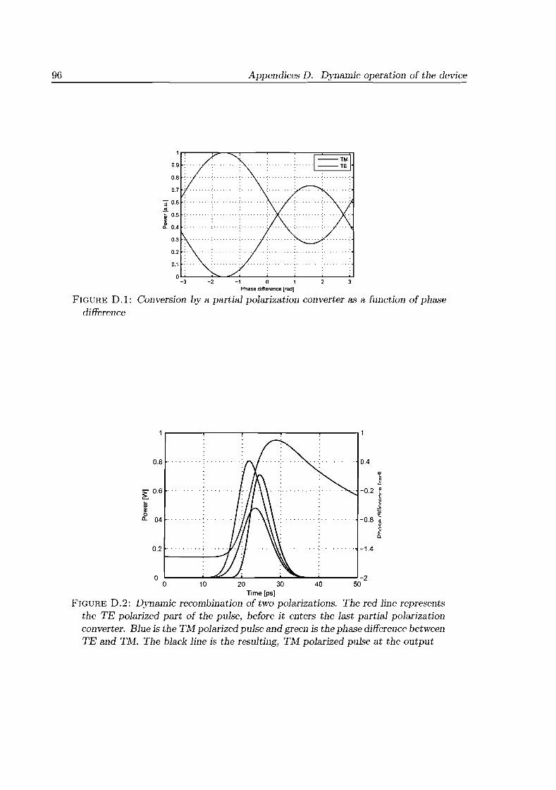
96
0.9
0.1
Appendices D. Dynamic operation of the device
:············I==~~I
O........--""""-......:::......---'------J'---.........--........-3 -2 -1 0 1 2
Phase difference [rad]
FIGURE D.l: Conversion by a partial polarization converter as a function of phasedifference
0.8 .
;[ 0.6
J 04 .
0.2 ..
0.4
-0.2 ~c~
~'i:
-0.8 Qun~
0.
-1.4
o ~o 10 20 30 40 50
Time Ips)
FIGURE D.2: Dynamic recombination of two polarizations. The red line representsthe TE polarized part of the pulse, before it enters the last partial polarizationconverter. Blue is the TM polarized pulse and green is the phase difference betweenTE and TM. The black line is the resulting, TM polarized pulse at the output

E
VARIABLE STEP SIZE INTEGRATION
Simulation of the polarization converters required an extra modification of the software integrating the differential equations that describe the process of polarization conversion. Thenumerical method used to solve the differential equations appeared to be unstable. Themethod was unstable because the differential equations describe a stiff problem. Stiffness ofa problem depends on the equations self, the initial conditions and the numerical methodused to solve them. Ordinary differential equations (ODEs) are stiff if their solution is slowlyvarying, but there are nearby solutions that vary rapidly, so that the numerical algorithm hasto take small steps, in order to find the solution. Although stiffness often causes problemsfinding a solution for a particular set of differential equations, it is more an efficiency issue.Non-stiff methods can solve stiff problems too, if their stepsize is small enough, but it willtake a lot of computational time to obtain satisfactory results.
The numerical method first used to integrate the rate equations was the fourth orderRunge-Kutta algorithm [14], which is what you use when you don't know any better or ifyou have a trivial problem where computational efficiency is of no concern. Runge-Kuttanearly always succeeds in solving the ODE problem provided, but it is not always the fastest.Proper numerical methods for solving ordinary differential equations should have some adaptive control over their own progress, by frequently modifying their stepsize. Often, the purposeof implementing adaptive stepsize is to achieve a predetermined accuracy, using a minimalamount of computational effort.
The technique used for stepsize adjustment is based on embedded Runge-Kutta formulas.It is a fact that Runge-Kutta formulas for orders M higher than four, require more thanM function evaluations. However, never more than M+2. Feldberg discovered a fifth-ordermethod with six function evaluations, where another combination of the six functions givesa fourth-order method. The difference between the two estimates of y(x + h) can then beused as an estimate of the truncation error to adjust the stepsize. The form of a fifth order
97

98
Runge-Kutta method is:
Appendices E. Variable step size integration
k l = hf(xn , Yn)
k2 = hf(xn + a2h , Yn + b2l kI)
(E.l)
k6 = hf(xn + a6h , Yn + b6l kl + ... + b6S ks )
Yn+l = Yn + clkl + C2 k2 + C3k3 + C4 k4 + csks + CBk6 + O(h6)
The embedded fourth-order formula is:
This leads to the following error estimate:
6
~ == Yn+l - Y~+l = L(Ci - Cnkii=l
(E.2)
(E.3)
The values for the constants Ci and C; that are favored, are those found by Cash and Karp.
Now that we have found an expression that gives us an approximate value for the truncation error, we have to find a way to keep it within certain desired bounds. To do this weconsider the relationship between ~ and h. From equations ?? and?? we find that ~ scalesas hS • If we now take a step with size hI and produce an error ~l, we can estimate the stepho that would have given an other value ~o with equation EA. We can use this formula intwo ways: if ~l 2: ~o, the equation tells how much to decrease the stepsize when we retrythe step. If ~l < ~o, the equation tells with how much we can safely increase the stepsizefor the next step.
I ~o 1°·2ho = hI ~l (EA)
The variable ~o is used as a vector of desired accuracies, one for each differential equation. The accuracy requirement is such that all the equations have to be within the allowederror range, so if we rescale the stepsize, this is done according the requirements posed by theequation with the biggest deviation.
Testing the differential equations of the polarization in Matlab as well as in the modelocked laser (MLL) software revealed that the numerical method used in the MLL softwarewas not capable of solving the system of equations without reducing the stepsize significantly.Reducing the stepsize would mean an enormous increase in computational time. This decreasein efficiency could be prevented by modifying the Runge-Kutta algorithm in such a way thatit uses a variable stepsize, which was therefor done.

F
MATLAB MODEL POLARIZATION
CONVERTERS
function ar=polc(start_cond);options=odeset('RelTol' ,le-8,'AbsTol',le-8);tspan = [0, 2.204*56]; % 0 .. Integration lengthar=ode45(@f,tspan,start_cond,options);
%figure;subplot(3,1,1);xlabel('Distance along polarization converter [\mum]');ylabel('Power [a.u.]');plot(ar.x(:),ar.y(l,:),'r'); % Plotting TE powerhold on;plot(ar.x(:),ar.y(2,:),'b'); % Plotting TM power
subplot(3,1,2);xlabel('Distance along polarization converter [\mum] ');ylabel('Phase [rad] ');plot(ar.x(:),ar.y(3,:),'r'); % Plotting TE phasehold on;plot(ar.x(:),ar.y(4,:),'b'); % Plotting TM phase
peff_te=ar.y(1,:)./(ar.y(1,:)+ar.y(2,:));peff_tm=ar.y(2,:)./(ar.y(1,:)+ar.y(2,:));
% Conversion efficiency TE% Conversion efficiency TM
subplot(3,1,3);xlabel('Distance along polarization converter [\mum] ');ylabel('Efficiency');plot(ar.x,peff_te,'r'); % Plotting conversion eff. TEhold onplot(ar.x,peff_tm,'b'); % Plotting conversion eff. TM
%------------------------------------------------------------
99

100
function dy = f(l,y)dy=zeros (4,1) ;
a=4166e-6;k=12724.77*le-6;d=4000e-6;
Appendices F. MATLAB model polarization converters
% Attenuation [l/um]% Coupling [l/um]% Phase mismatch[l/um]
dy(1)dy(2)dy(3)dy(4)
-2*k*sqrt(y(1)*y(2))*sin(y(3)-y(4))-2*y(1)*a;2*k*sqrt(y(1)*y(2))*sin(y(3)-y(4));
= -(k*sqrt(y(2)/y(1))*cos(y(3)-y(4))+d);-(k*sqrt(y(1)/y(2))*cos(y(3)-y(4))-d);
%dy(1)%dy(2)
-i*k*y(2)+i*d*y(1)-a*y(1);-i*k*y(1)-i*d*y(2);
% Coupled mode theory TE% Coupled mode theory TM

G
MATLAB MODEL SELF PHASE
MODULATION
function ps=calcspm(Ul, U2, aN, t, gamma, N);
q=1.60e-19;w=3e-6;NO=1.50e24;h=6.63e-34;c=3.00e8;lambda=1550e-9;alpha=5;epsilon= 0.2;
L=le-6:1e-6:1.5e-3;
% Electron charge%Width of the active region%Transparency carrier density%Planck constant%Speed of light%Wavelength%Linewidth enhancement factor%Non linear gain coefficient
%Sweep length from 1 um to 1 rom
gO=gamma*aN*NO*log(N/NO); %Unsaturated gainGO=exp(gO*L); % Gain integrated over the lengthUsat= (h*c/lambda) * (w*t/gamma)/aN/epsilon; %Saturation energyargl=l-(l-l./GO)*exp(-Ul/Usat); %Phase first part of the pulsearg2=1-(1-1./GO)*exp(-U2/Usat); %Phase second part of the pulse
ps=(1/2)*alpha*log(argl./arg2);% Phase difference
plot(L./le-6,ps); % Plot the phase difference
101