electrical characterisation of cmos ring oscillatordmh/4b7/resource/ring/4b7e2512.pdfperformance of...
TRANSCRIPT
Performance of CMOS ring oscillator (v) 1 D M Holburn January 2012
Engineering Tripos Part IIB FOURTH YEAR
Module 4B7: VLSI Design, Technology, and CAD
Laboratory Experiment
Electrical Characterisation of CMOS Ring Oscillator
This pamphlet describes a laboratory activity based on an integrated circuit originally
designed and tested as a student project. Its purpose is the measurement of the switching
speed of some CMOS logic gates on a 2 µm n-well technology silicon integrated circuit. The
MOSFETs employed have threshold voltages of ±1 volt approximately. You will have an
opportunity to investigate the behaviour of these circuits as a function of supply voltage and
in a range of configurations, and compare with simulated results.
This coursework counts for 25% of the available credit for the module. Please make the report at most four pages long. You
may include extra pages of data, graphs and images above the total. Hand in your report, this experiment sheet, and a
completed cover sheet, to the cabinet outside the EIETL by 5pm on Monday, 30th April 2012. Late reports will incur a penalty
and in extreme cases may not be marked.
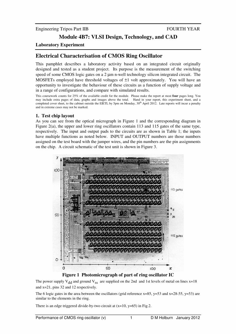
1. Test chip layout As you can see from the optical micrograph in Figure 1 and the corresponding diagram in
Figure 2(a), the upper and lower ring oscillators contain 113 and 115 gates of the same type,
respectively. The input and output pads to the circuits are as shown in Table 1; the inputs
have multiple functions as noted below. INPUT and OUTPUT numbers are those numbers
assigned on the test board with the jumper wires, and the pin numbers are the pin assignments
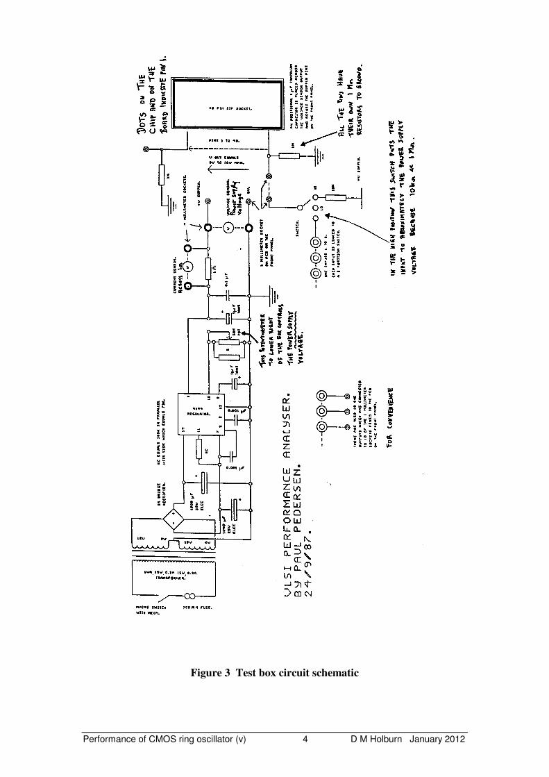
on the chip. A circuit schematic of the test unit is shown in Figure 3.
Figure 1 Photomicrograph of part of ring oscillator IC
The power supply Vdd and ground Vss are supplied on the 2nd and 1st levels of metal on lines x=18
and x=21, pins 32 and 12 respectively.
The 6 logic gates in the area between the oscillators (grid reference x=85, y=53 and x=28-55, y=53) are
similar to the elements in the ring.
There is an edge triggered divide-by-two circuit at (x=10, y=65) in Fig.2.

Performance of CMOS ring oscillator (v) 2 D M Holburn January 2012
Input Description Grid Ref
INPUT 3 (pin 3) Controls element 1 of ring-113
Controls element 1 of ring-115
Controls one input to the single device
(x=100, y= 66)
(x=108, y=400)
(x= 85, y= 53)
INPUT 4 (pin 4) Controls three elements of ring-113 (x= 40, y= 66)
(x=108, y= 66)
(x=108, y= 97)
INPUT 2 (pin 39) Controls element 115 of ring-115
Controls one input to the single device
(x=115, y= 40)
(x= 85, y= 53)
OUTPUT 5 (pin 5) From the single device (x= 85, y= 53)
OUTPUT 6 (pin 6) From the ring-113, after an extra
buffer element
(x= 30, y= 91)
OUTPUT 7 (pin 7) From the ring-113, after an extra
buffer element
(x= 30, y= 65)
OUTPUT 8 (pin 8) From the divide-by-two circuit which
has output 9 as its input
(x= 10, y= 65)
OUTPUT 9 (pin 9) From the fifth logic gate in the line
(no buffer element)
(x= 26, y= 53)
OUTPUT 10 (pin 10) From the ring-115 after element 16
after an extra buffer element
(x= 30, y= 40)
Table 1 Input and output pins
Figure 2 Ring Oscillator Circuit Schematic
Performance of CMOS ring oscillator (v) 3 D M Holburn January 2012
2. Experimental Procedure: Testing the single device.
Important: Be sure to use Box A for sections 2-8.
Before measuring the ring oscillator we shall first test the single two-input gate (x=85, y=53),
which is identical to the gate on which both rings, 113 and 115, are based. Ensure that the
measurement box in Fig. 3 contains a chip with design 21. All inputs and outputs are
applied/observed through input or output pads, which are inverting and introduce delay.
To change chips, move the lever over to release the pins, lift out the chip (without touching the pins -
this could damage the circuit by electrostatic discharge). Push the pins into the pad of protective black
conductive foam for storage, mount chip with dots aligned, and pull the lever to clamp the pins.
The supply voltage can be set to values in the range 0.2 – 9 V approximately using the
control knob at lower right on the test box. The meters provided allow accurate measurement
of supply voltage and current. NB current is sensed by measuring the voltage drop across a
1Ω resistor – see Fig 3 – the meter must be set to measure voltage and the result converted
mentally to a current. Setting the meter to a current range will give incorrect results.
• Please record the serial number of your chips: (e.g. 21-10) .
• Ensure that the positive power supply is connected to pin 32 on the chip and the ground is
connected to pin 12. Set the power supply VDD to 3V.
• Set INPUT 3 (pin 3) HIGH. Later, try with it set to LOW, to determine the truth table.
Owing to the I/O pads, the three-way switch in the left position (labelled HI) to any input
applies a LOW input at the internal circuit. Note: switches are not debounced and will
generally introduce multiple pulses into the ring.
• Set INPUT 4 (pin 4) LOW (to disable ring 113).
• Feed a square wave to INPUT 2 (pin 39) (switch set to the right - BNC input), amplitude
about 3V, frequency about 1MHz
• Sketch what you observe when OUTPUT 5 and INPUT 2 (pin 39) are displayed together
on a dual trace oscilloscope.
• Hence, deduce the truth table and thus the logic function performed by the single gate.
• Use the oscilloscope to estimate the delay of the single gate. What factors (three or more)
limit the accuracy you can expect to achieve?
3. Testing ring-115.
Ring oscillators ring-113 and ring-115 are made up of 2-input gates identical to that
examined in section 2; ring-115 has two inputs which can be used to control the oscillation.
First examine the behaviour of the ring when free-running with VDD at 3V.
• Set INPUT 2 (pin 39) to HI to allow the ring to free-run. Trigger the oscilloscope with
OUTPUT 10 and observe the waveform.
Caution: The ring may go into a high order resonance owing to switch contact bounce. If so,
first set INPUT 3 to LO to stop the ring and then set it to HI again. You may need to repeat this
procedure more than once. Alternatively, with the switches set as required, reduce the supply
voltage to zero and bring it up gradually to the desired value. This normally achieves a smooth
start to the oscillations. You are strongly recommended to monitor all output waveforms
using the oscilloscope, to guard against inadvertently selecting a harmonic mode.
Now investigate how the oscillation can be gated on and off by means of a pulse train.
• With the square wave connected to INPUT 2 (pin 39), adjust the input frequency at
INPUT 2 (pin 39) to about 100kHz with a duty cycle of 50%.
• With the switch at INPUT 2 (pin 39) set to INPUT, observe OUTPUT 10 and INPUT 2
(pin 39) on the oscilloscope, using the input as a trigger. Sketch the waveforms.
Show how to use this approach to determine the ring frequency as a multiple of the pulse
frequency, and record the ring frequency obtained in this way.
Performance of CMOS ring oscillator (v) 4 D M Holburn January 2012
Figure 3 Test box circuit schematic
Performance of CMOS ring oscillator (v) 5 D M Holburn January 2012
4. Determining the gate delay by measurements on ring-115 and ring-113.
With the setup of section 3, carry out the following experiments:-
• Make a rough measurement of the period of the high-frequency oscillations using a direct
reading from the screen of the oscilloscope.
• With VDD set to 3V, and using the most suitable method from those above, determine the
natural ring oscillator frequency (counter-timer or oscilloscope), and find the gate delay
per stage in the ring, making sure that you are not in error by a factor of 2!
• Now using ring-113, investigate a further way to estimate the gate delay. Display
OUTPUTS 7 and 6 on the dual trace oscilloscope, set ring-113 oscillating and divide the
observed delay by the number of intervening gates.
• Find the number of gates by counting the gates in Figure 2, bearing in mind that the buffer
gates connected to each output are external to the ring.
• Does OUTPUT 7 come before OUTPUT 6, or vice versa?
Compare and contrast the methods explored in sections 2 - 4 for obtaining the gate delay.
5. Measure the effect of varying the power supply voltage.
The switching characteristics are expected to depend on the supply voltage VDD. In this
section you will make a detailed investigation of the nature of the variation over a wide range
of voltages.
• First, determine the minimum power supply voltage required to establish full-amplitude
oscillations by setting the switches so that only one ring free-runs, the other ring being off.
• Measure the frequency of the free-running ring using the frequency counter as the power
supply voltage is varied. Plot the result and note the rate of change in frequency with
power supply voltage VDD at 3 V.
• Interpret your plot of frequency vs. ring voltage. Is it an accurate straight line? What
evidence is there of:
(a) anomalous behaviour at high VDD (i.e greater than 5 V)
(b) subthreshold operation: | VT | is approximately 1 V for both n and p devices
Determine the lowest frequency at which oscillations can be detected.
Attempt to account for any interesting phenomena you observe.
• “The power consumption of this design is substantially dynamic in nature, proportional to
½ CVDD2, since all gates are digital and drive capacitive loads”. By consideration of the
variation of chip supply current with VDD, investigate this statement. Does it hold true?
Use this information to make a reasonable estimate of the total capacitance being driven
by the circuit.
6. Performance comparison with different transistors in the ring
As explained, test chip designs 28 and 21 have similar transistors in the elements of the ring
oscillators except that the p-channel transistors in design 28 are three times wider than those
in design 21. This affects both the on-state channel conductance and the capacitive load
presented to the previous stage of the ring.
To change chips, move the lever over to release the pins, lift out the chip (without
touching the pins as this could damage the circuit by electrostatic discharge). Push the
pins into the pad of protective black conductive foam for storage, mount the new chip
with the dots aligned, and pull the lever to clamp the pins.
What is the percentage difference in performance between the designs at supply voltage VDD
= 3 V and VDD = 5 V? Explain on the basis of the transistor dimensions why you would
expect a difference, and estimate the magnitude of the expected change. Make reasonable
assumptions (with explanations) about parameters not explicitly stated.
Performance of CMOS ring oscillator (v) 6 D M Holburn January 2012
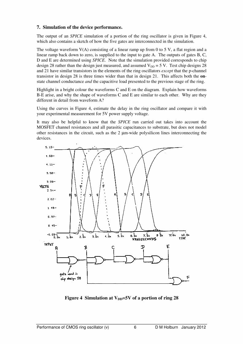
7. Simulation of the device performance.
The output of an SPICE simulation of a portion of the ring oscillator is given in Figure 4,
which also contains a sketch of how the five gates are interconnected in the simulation.
The voltage waveform V(A) consisting of a linear ramp up from 0 to 5 V, a flat region and a
linear ramp back down to zero, is supplied to the input to gate A. The outputs of gates B, C,
D and E are determined using SPICE. Note that the simulation provided corresponds to chip
design 28 rather than the design just measured, and assumed VDD = 5 V. Test chip designs 28
and 21 have similar transistors in the elements of the ring oscillators except that the p-channel
transistor in design 28 is three times wider than that in design 21. This affects both the on-
state channel conductance and the capacitive load presented to the previous stage of the ring.
Highlight in a bright colour the waveforms C and E on the diagram. Explain how waveforms
B-E arise, and why the shape of waveforms C and E are similar to each other. Why are they
different in detail from waveform A?
Using the curves in Figure 4, estimate the delay in the ring oscillator and compare it with
your experimental measurement for 5V power supply voltage.
It may also be helpful to know that the SPICE run carried out takes into account the
MOSFET channel resistances and all parasitic capacitances to substrate, but does not model
other resistances in the circuit, such as the 2 µm-wide polysilicon lines interconnecting the
devices.
Figure 4 Simulation at VDD=5V of a portion of ring 28

Performance of CMOS ring oscillator (v) 7 D M Holburn January 2012
8. Stroboscopic pulse generator
This experiment requires a little extra determination! However, carefully carried out, it will
give a deep insight into the subtleties of the performance of the circuit, and of the accuracy of
the simulation results that guided its design. It involves running both ring oscillators
simultaneously, a mode of operation not necessary in earlier experiments. Small changes in
supply voltage can have a dramatic effect on your observations, owing to the strong
dependence of gate delay on VDD. Also, chip designs 21 and 28 have slightly different
characteristics and it may sometimes be easier to observe the effects on chip design 28.
In the schematic of Figure 4, the sense gate F with inputs from E and B gives a high output
only when both inputs are low. This function is also realised on the chip by the gates at
(x=40, y=53) and at (x =55, y=53). The result appears at OUTPUT 9 (pin 9). There is also
an edge-triggered divide-by-2 circuit on the chip at (x=15, y=60). Its input is internally
connected to OUTPUT 9 and can be monitored at OUTPUT 8 (pin 8).
Given that the sense gates on the chip each span 5 elements of the rings (note that in the
specimen circuit of Figure 4, only 3 are spanned):
• Describe the circumstances in which the output from each sense gate will be in the logic
HIGH state during normal operation of the rings.
• What output do you expect from OUTPUT 9 of chip design 28 in Figure 2 when:-
a) ring-113 and ring-115 are running freely with the same VDD – consider what their
relative frequencies are expected to be;
b) when INPUT 4 is LOW (i.e. HIGH after inversion at the input pad), and ring-115 alone
is running?
• Verify your predictions by experiment using the procedure below. Change to chip
design 28 only if necessary.
• First, observe OUTPUTS 10 and 9 on the oscilloscope with both rings free-running. To
achieve this, switches at INPUTS 2-4 must be set to HI. Use a low supply voltage of
approximately 0.6 - 0.7 V, and guard against either ring entering a harmonic mode. Once
you have observed the sense waveform, consider applying it to the oscilloscope’s External
Trigger input so you can monitor both ring outputs in the vicinity of the sense signal.
• Confirm that the circuit performs the expected function over a small range of supply
voltages and increase/decrease the power supply voltage until it just no longer works.
Record your observations.
• Next, observe OUTPUTS 10 and 9 on the oscilloscope with a fairly low power supply
voltage, and ring-115 only in operation. To achieve this requires the switches at INPUTS
4, 3 and 2 (pin 39), set LO, HI and HI respectively. Investigate the divide-by-2 output, at
OUTPUT 8 (pin 8), and show that it works as expected over a range of supply voltages,
and record the range. Outside this range the rise/fall of the input edge may be too slow or
too fast to clock the divide-by-2 stage.
• If the range of operating voltages for the divide-by-two and the strobe pulse generator
overlap, you should be able to set the switch at INPUT 4 HI again, and observe the strobe
pulses divided by two, at a suitably chosen VDD. However, it is possible you will come to
the conclusion that the operable ranges do not coincide. Full operation is only possible on
a few sample chips where fabrication tolerances dictate. This idiosyncratic behaviour
could not be predicted by the simulation tools.
• With a higher supply voltage in the range 2-4 V and both rings oscillating, observe their
outputs critically using the oscilloscope connected to OUTPUT 10 (pin 10) and OUTPUT
6 (pin 6). Can you see evidence of noise or interference superimposed on the digital
signals? Why might these be present?
Performance of CMOS ring oscillator (v) 8 D M Holburn January 2012
9. Ring oscillators with realistic loads on the devices in the ring (Optional)
The second measurement box provided (Box B) has been developed for the purpose of
investigating the behaviour of ring oscillators operating under more realistic and variable
loading conditions. It relies on a CMOS device specifically designed and fabricated for the
purpose.
Note: the process dimensions used are not the same as those for chips 21 & 28.
The measurement box has additional switches to select one of a number of ring oscillators,
and a precision potentiometer for adjusting the supply voltage. In other respects it resembles
the unit used to test chips 21 & 28.
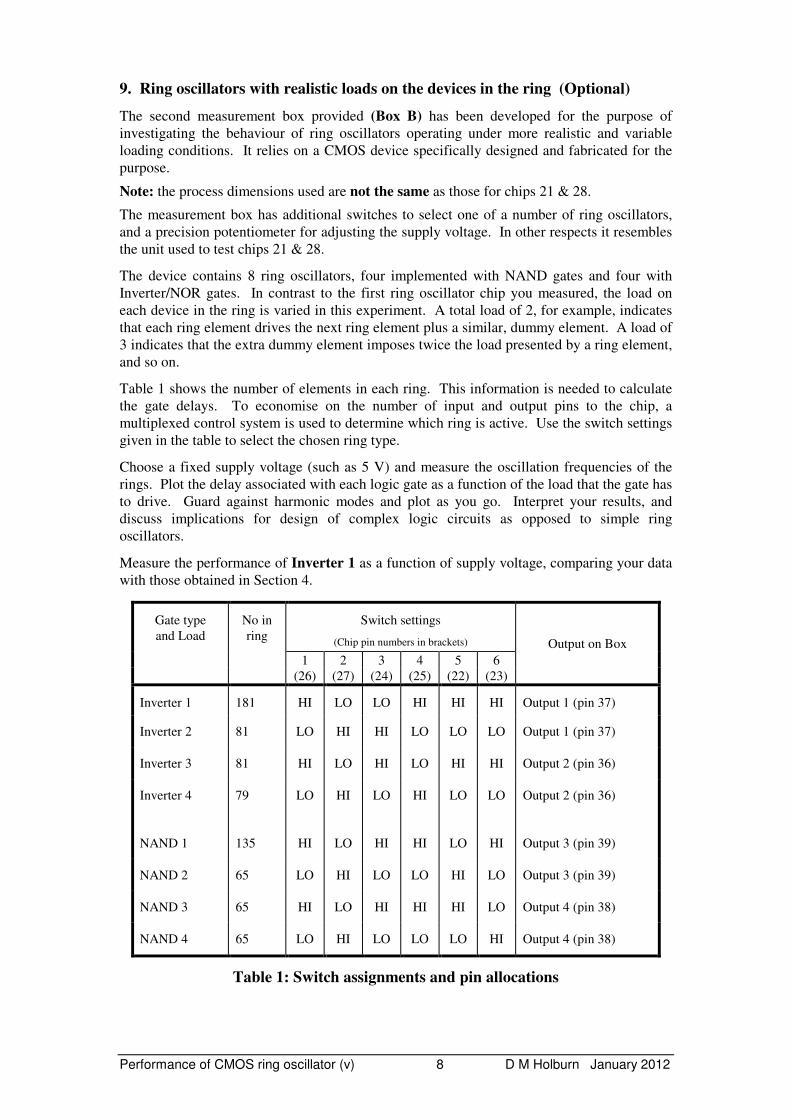
The device contains 8 ring oscillators, four implemented with NAND gates and four with
Inverter/NOR gates. In contrast to the first ring oscillator chip you measured, the load on
each device in the ring is varied in this experiment. A total load of 2, for example, indicates
that each ring element drives the next ring element plus a similar, dummy element. A load of
3 indicates that the extra dummy element imposes twice the load presented by a ring element,
and so on.
Table 1 shows the number of elements in each ring. This information is needed to calculate
the gate delays. To economise on the number of input and output pins to the chip, a
multiplexed control system is used to determine which ring is active. Use the switch settings
given in the table to select the chosen ring type.
Choose a fixed supply voltage (such as 5 V) and measure the oscillation frequencies of the
rings. Plot the delay associated with each logic gate as a function of the load that the gate has
to drive. Guard against harmonic modes and plot as you go. Interpret your results, and
discuss implications for design of complex logic circuits as opposed to simple ring
oscillators.
Measure the performance of Inverter 1 as a function of supply voltage, comparing your data
with those obtained in Section 4.
Gate type
and Load
No in
ring
Switch settings
(Chip pin numbers in brackets)
Output on Box
1 2 3 4 5 6
(26) (27) (24) (25) (22) (23)
Inverter 1 181 HI LO LO HI HI HI Output 1 (pin 37)
Inverter 2 81 LO HI HI LO LO LO Output 1 (pin 37)
Inverter 3 81 HI LO HI LO HI HI Output 2 (pin 36)
Inverter 4 79 LO HI LO HI LO LO Output 2 (pin 36)
NAND 1 135 HI LO HI HI LO HI Output 3 (pin 39)
NAND 2 65 LO HI LO LO HI LO Output 3 (pin 39)
NAND 3 65 HI LO HI HI HI LO Output 4 (pin 38)
NAND 4 65 LO HI LO LO LO HI Output 4 (pin 38)
Table 1: Switch assignments and pin allocations