electrical principles 119 control - ed thelened-thelen.org/comp-hist/ibm-603-g-elect-119-144.pdf ·...
TRANSCRIPT

E L E C T R I C A L P R I N C I P L E S 119
Ten-Pulse Control
Up to the time the multiplier carries, no other
operation takes place. When a carry occurs, it is a signal to start rolling the multiplicand counter.
Before discussing the multiplicand read-out, it is
necessary to establish the 10-pulse control circuit
together with its associated circuits. Since several of these circuits are interconnected, they will all
be discussed at this point.
First, consider the A33 switch tube (Section
24A) which produces negative pulses at 10 and
14 to turn trigger B3 (Section 27B) ON and OFF.
The status of B3 trigger is indicated by indicator
light 5 on the socket B7. The circuits for A33 and B3 are shown in Figure 1 12.
Switch A33 can conduct only when both the
grid and suppressor are above cutoff. The grid of A33 is normally at about -35 volts and will rise
above cutoff when it receives a positive pulse from
tube A271 of trigger A27, the second stage of the
primary timer. This positive pulse will come every
time A27 goes ON, i.e., at 2, 6, 10, and 14 of each
primary cycle. However, the tube cannot conduct
unless the suppressor also rises above cutoff. The suppressor is directly coupled to the anode of tube
A341, which is a follower for the OFF side of trig-
ger A29, the fourth stage of the primary timer.
As long as A29 is OFF, A341 is conducting, and its
anode potential is low (approximately + 50 volts).
As long at A341 conducts, then the suppressor of
A33 is at approximately -50 volts which is below
cutoff for this element. When A29 goes ON, A341
stops conducting, and its anode potential rises to
approximately +I50 volts. The suppressor A33
is then above cutoff, and conduction occurs
through A33 subject t o the pulses applied to the
grid. Since the suppressor will be conditioned to
conduct by A341 from 8 through 0, of the four
pulses received by the grid, only two can cause
conduction, those at 10 and at 14.
When A33 conducts at 10 and at 14, it pro-
duces negative pulses at its anode. These negative
pulses are fed to both sides of trigger B3 from the
midpoint of the A33 load resistor. The -10 pulse
turns B3 ON, which is initially OFF by cancelling.
The -14 pulse again turns B3 OFF. Therefore B3
goes ON at 10 and OFF at 14 of each primary cycle.
Trigger B3 through its followers B91 and B92
controls several circuits among which is the 10-
pulse control. Follower B91 follows the ON side of
trigger B3 and thus produces a -10 pulse and +14
pulse. The purpose of these pulses will be explained
later. Follower B92 follows the OFF side of B3;
consequently, it is conducting at all times except
from 1 O through 14. From 1 O through 14 the
anode potential of B92 is high to condition certain
switches. At 14 the negative pulse at the
midpoint of the B92 load resistor is passed on to the
secondary timer to advance it 1 for each primary
cycle.
One of the switches conditioned by B92 is BIO,
as shown on the B chassis diagram (Section 28B)
and in Figure 113. In other words, B10 is recep-
tive to pulses applied to its suppressor from 10
through 14. A constant stream of B pulses is ap-
plied to the suppressor of BlO, and remembering
that B pulses are negative at index points and posi-
tive at mid-index points, it is obvious that B1O will
conduct on every positive B pulse from 10 through
14, or at 10.5, 11.5, 12.5, and. 13.5, as shown on the timing chart in Figure 1 13. Before discussing
the purpose of these pulses, examine B4 switch
(Figure 113) which works with B10 switch to
control B16 trigger. B4 also receives a constant
stream of B pulses at its suppressor, but its grid is
conditioned by A342, which is a follower for the
ON side of trigger A29 (the fourth stage of the
primary timer). The anode of A342 is at high po-
tential as long as A29 is OFF, i.e., from O through
8; hence B4 switch is conditioned to conduct from
O through 8 and will conduct on the positive shifts
of the B pulses at 0.5, 1.5, etc., through 7.5, as in-
dicated on the timing chart in Figure 113. A t
each of these points a negative pulse is produced
at the anode of B4. This pulse is taken from a tap
on the load resistor of B4 and fed to the OFF side

120 T Y P E 6 0 3 E L E C T R O N I C M U L T I P L I E R
ij w a - , N N 2 n o , O ' D
I I I I a m m m m

E L E C T R I C A L P R I N C I P L E S 121
( Lost slog* Of) PO* I
T
M'Plier M,Cond Reodout Output Control Trigger Inverter
(Fue.1) ON when MIPller Carries
OFF 01 end of Col. Shift Cycle To Anode 8-112
T I To Grid
.02
8-17 8-11
I : I r
-100 I 1 I ! I I - 100
-100 Consel
-100
1 Cancel
To Anode 8-23 (Loet Ologe 01 Secondory Timer1
Figure 114. Multiplier Output Circuit
of trigger B16 which is initially OFF by cancelling.
The first of the series of pulses at 0.5 will turn B16
D ON and the others will have no effect until B16 is
again rurned OFF. Since B16 does not turn OFF
before 8, only the 0.5 pulse is used, and it turns
B16 ON.
Now observe that the ON side of B16 is coupled
to the output of switch B1O which was just dis-
cussed. It has been shown that B10 produces
negative pulses at 10.5, 11.5, 12.5, and 13.5. The first of these pulses, -10.5, will turn B16 OFF, and
the others will have no effect. It has been deter- mined then that B16 turns ON at 0.5 of each pri-
mary cycle and turns OFF at 10.5 of each primary
cycle, thus providing the timing control for pro-
ducing 10 adding pulses each primary cycle.
Multiplicand Counter Rolling Control
I t has been shown that B16 provides a means of
producing 10 pulses for rolling the multiplicand,
but it must be remembered that these 10 pulses
cannot be fed to the mulbtiplicand counter every primary cycle, but only on those Primary cycles following a carry-over in the multiplier position determined by t b column shift control. Conse-
) quently, it is evident that some means must be
provided to signal when this is to happen.
Figure 114 shows the circuits for multiplier
read-out control using the first position of the
multiplier counter. As noted in Figure 114 the
multiplicand rolling control trigger, B17, is in
the B chassis and is located in Section 28B of the
wiring diagram. Indicator light 3 in socket B7
indicates the status of rhis trigger. The multiplier
output inverters are in the H chassis which con-
sists of three 12SN7's. One triode section of each
tube in the H chassis is used for each position of
the multiplier counter.
Observe that no load resistors are shown in the
H chassis circuit diagram (Section 41). All six
triode inverters use the same load resistor, which
is shown to the right of B17 trigger in the B chas-
sis diagram. This common load resistor is permis-
sible, because only one multiplier position can be
active at any one time; hence only one tube in the
H chassis can use the load resistor at any one time.
The common load resistor also permits all six mul-
tiplier output inverters to control the same trigger.
Referring now to Figure 114, note that only the
last stage trigger of the multiplier counter position
1 is shown. Observe also that the grid of HI1 is
at approximately -3 5 volts, as determined by the
voltage divider between the -100 volt line and
pound. This means that HI1 is normally cut off,

122 T Y P E 6 0 3 E L E C T R O N I C M U L T I P L I E R
and its anode is a t high po~ential. When the mul-
tiplier counter position being advanced goes from
9 t o 0, trigger E4 goes OFF and a positive pulse
appears at the anode of tube E4a. This positive
pulse is transmitted through the 100 mmfd
coupling capacitor to the grid of H11, momen-
tarily driving it above cutoff and causing H I 1 to
conduct. When H I 1 conducts, a -100 volt nega-
tive pulse is produced at its anode. From the mid- point of the load resistor of H I 1 a -50 volt nega-
tive pulse is fed t o the OFF side of trigger B17,
which is initially cancelled OFF. This negative pulse turns B17 ON, and the follower tube B l l l
is in Turn cut off. B17 remains in the ON status
until turned OFF at 14 of the last primary cycle
in the given column shift cycle. B17 is turned OFF by a negative pulse produced at the anode of
tube B231, which is the OFF side of the last stage
of the secondary timer. The negative pulse at the
anode of B231 appears when the secondary timer
advances from 9 to 0, signalling a column shift.
From the foregoing description, it may be seen that B17 turns ON at 12 of the primary cycle dur-
ing which the active multiplier position advances
from 9 to 0, and B17 stays ON until the end of that
column shift cycle. B17, then, determines the
number of primary cycles during which 10 rolling
pulses are applied t o all positions of the multipli-
cand counter. Follower tube B111 for B17 trigger
and follower .tube B112 for B16 trigger work to-
gether as blocking tubes to control the 10-pulse
control switch BY, as shown in Figure 11 5 and in
Section 28A of the circuit diagram. B112 is a t high potential from 0.5 through 10.5 of every p i - 77znrj1 cycle, since it follows athe OFF side of B16
trigger, the 10-pulse control trigger. However,
3 11 does not permit BI 12 to be effective until
after trigger B17 turns ON, indicating thax the
multiplicand must start receiving rolling pulses.
Then, during every primary cycle after 317 turns
ON, the anode potential of both Bl la and B111 is
high from 0.5 through 10.1, and the grid of 3 5 switch is conditioned to conduct accordingly. Ob-
serve that the grid of B5 is a t approximately -50
volts as long as either B112 or B111 is conducting.
When both Bl la and Bill are cut off, the grid of
B5 rises well above curoff and B5 is conditioned
to conduct subject to the positive pulses applied t o
the suppressor.
The suppressor of BY is normally at -50 volts
as determined by the voltage divider between
ground and -100 volts. The suppressor BY is
coupled by means of a 250 mmfd capacitor t o the
anode of A16, where A pulses are produced; hence
the suppressor of BY receives a constant stream of
A pulses a t its suppressor, and B5 will conduct on
every positive shift of the A pulses from 0.5
through 10.5. As indicated on the timing chart
in Figure 11 5 , B5 will produce 10 .negative B
pulses at its anode during each primary cycle thax
it is active. These negative pulses at 1, 2, 3, etc.
through 1 O are fed by way of a T O mmfd coupling
capacitor to the grid of the 25L6 power tube, B6.
The grid of B6 is tied .to + 150 volts through a .47
megohm resistor and consequently B6 is normally
conductive. Each time B5 conducts, a negative
pulse is passed to the grid of B6, cutting off B6
momentarily and producing a positive pulse at the
anode of B6. Thus, 10 positive A pulses are pro-
duced at the anode of B6 during each primary
cycle that B17 is turned ON. These are the 10
pulses used to roll the multiplicand counter. From the section on Read-172 Circuits i t will be
remembered that the D chassis contains the in-
verters controlling the read-in of the 10 rolling
pulses. There is one inverter for each position of
the multiplicand counter, and each consists of one
triode section; therefore only three 12SN7's are re-
quired. These are D5, D l 1, and D14. The in-
verter grids are normally at -35 volts, and each
time a positive A pulse from 3 6 is fed to the p i d s
of the six inverters through the 250 mmfd coup-
ling capacitor, all six inverters conduct and pro-
duce negative pulses at their anodes. These negative
pulses are taken from the midpoint of the inverter
load resistors and passed t o the six positions of the

E L E C T R I C A L P R I N C I P L E S 123

124 T Y P E 6 0 3 E L E C T R O N I C MULT IPL IER
MqCond ( Assume '3" in M'Cond Counter)
Corry 1 place tokes here ( - 0 Pulws) T
-10 Rolling Pulses Received by MICand+
(+B Pulses1 10 Pulsar Fed to Col. Shift Switches
(-A Pulses) 3 Pulses Receivad by Product Counter
Pulse control
'3' in counter 1
FN'I Pulse M'Cond
a t 10 Output Triggers
I
Col. Shift Switches control
Product Counter
MlCond Counter
~ b d i n g stops a t 10
Start Switch
,0-"0" PulSes
Figure 116. Multiplicand Output to Product
,--- M'Plier Carryover
multiplicand counter. Thus, each position of the of the number standing in the counter. When the
multiplicand counter receives 10 rolling pulses multiplicand is transferred to the product counter,
during each primary cycle that trigger B17 is ON. entry pulses to the product counter start ar half
Power tube B12 operares exactly as does B6 ex- a cycle point after the multiplicand position being
cept thar it inverts negative A pulses to positive read out arrives at zero, and terminates at 10 of
B pulses to feed the column shift control power the cycle. For instance, if a multiplicand counter
tubes. The column shift conrrol will be discussed position contains a 2, the eighth entry pulse applied
in succeeding sections. B12 is shown at 27A of to this position (at 8 of the cycle) advances it to
the wiring diagram. 0. This enables 2 entry pulses to be applied to the
product counter, one pulse at 8.5 and another at Multiplicand Read-Out 9.5 of the adding cycle. Similarly, a 3 standing in
The number of entry pulses required to advance the muitiplicand enables the product counter to
a counter position to zero is the ten's complement receive 3 pulses, at 7.5, 8.5, and 9.5. This is shown

E L E C T R I C A L P R I N C I P L E S 125
To Anode 8-2
Poe. I M'Cond Counter ( Lost slope Of Pas. I )
Pulse M'Cond Output Follower Tripper
.51 = - 4 0
To Grids of to lurnn~hi f t Switches
.o2
.47
+ 150
0
-100
Figure I 1 7 . Multiplicand Read-out Controls
in Figure 116 which is a block diagram of the mul-
tiplicand read-out operations. Remember that
positive A pulses are fed to the multiplicand input
inverters, which in turn invert them to negative
B pulses to operate the multiplicand counter trig-
gers. This means that the multiplicand carry-over
occurs at index points of the primary cycle. How-
) ever, the pulses fed to the product counter by the
column shift control switches are negative A pulses
coming at mid-index points of the primary cycle.
This arrangement permits the multiplicand read-
out triggers to turn ON and condition the column
shift switches one-half cycle point before any
pulses are passed by the switches.
Figure 1 17 shows the multiplicand read-out cir-
cuit for the first position of the multiplicand
counter. Only the last stage of the counter posi-
tion is shown. When the first position of the mul-
tiplicand counter advances from 9 to 0, trigger I4
goes OFF, and a negative pulse appears at the anode
of tube 141. A -TO volt pulse at the midpoint of
the load resistor for 141 is passed on to the OFF
side of trigger L2, turning it ON. When L2 goes
ON, tube L21 cuts off, and follower tube L41 does
likewise. As long as L41 is cut off, its anode is at
Thus, the column shift switches are permitted to
conduct when L2 trigger goes ON. It might be
noted that on the main wiring diagram the .TI
megohm resistors are shown in the L chassis circuit,
while the .47 megohm resistors are shown on the 0 chassis circuit. This arrangement permits the grids
of the 6SK7 switches in the 0 chassis to be tied
down below cutoff in case jumper wires between
chassis are removed. At a given point in the cycle all adding in the
product counter must be stopped, so that only the
correct number of pulses enter the product counter.
The adding is stopped by turning the multiplicand
read-out triggers OFF at 10. AS shown in Figure
117, a + l o pulse is fed through the .02 mfd
covpling capacitor to the grid of L42, which is nor-
mally cut off. The +I0 pulse causes momentary
conduction through L42. Observe that the anode
of L4- is tied to the anode tube 1 of trigger L2,
indicating that L42 uses the same load resistor as
the L21 tube. When L42 conducts, the potential at
its anode drops, and the potential at the anode of
tube L21 also drops. This causes L2z.to stop c9n-
ducting and triggering results. Therefore, causing
L42 to conduct will turn L2 OFF, if it happens to
high potential, and the midpoint of the voltage be ON.
divider in parallel with the load resistor L41 is at In addition to turning L2 OFF at 10, L4r serves approximately +25 volts. This midpoint is con- as a blocking tube to prevent L2 from turning ON
) nected to the grids of all the column shift switch when a O is transferred. When a O is transferred,
tubes for the first position of the multiplicand. no pulses should get t o the product counter; con-

T Y P E 6 0 3 ELECTRONIC MULTIPLIER

E L E C T R I C A L P R I N C I P L E S 127
sequently, trigger L2 should not turn ON. With a O in the first po'sition of the multiplicand, the
multiplicand counter position will signal a carry at
10 of the cycle. This would normally turn L2 ON.
A t 10, however, L4 is conducting because of the
+ l o stop pulse. This means that L2 is blocked
from turning ON, since the potential gt the anode
of the tube L21 cannot rise as long as L42 is con-
ducting.
The + l o pulse mentioned is produced by tube
B2 in the B chassis (Section 27A). I t will be re-
membered from the discussion of trigger B3, that
follower B91 follows the ON side of trigger B3,
which is ON from 10 through 14. Consequently,
B91 will produce a negative pulse at 10 and a posi-
tive pulse at 14. The -10 pulse is passed to the
grid of B2 via a 50 mmfd coupling capacitor. B2
is normally conducting, since its grid is tied to
$150 volts through a .47 megohm resistor. The
-10 pulse from B91 momentarily cuts B2 OFF, and
its anode potential rises abruptly from about 4-50
volts to + 150 volts. This positive pulse at 10 is
passed to the L chassis to turn all the multiplicand
read-out triggers OFF.
Figure 118 is a block diagram showing tube ar-
rangement and operation of multiplicand rolling
and output circuits. This diagram should be studied
in conjunction with the block diagram in Figure
111.
Column Shift Switches
When the multiplicand factors are transferred
to the product counter, they must be entered in
different positions of the product counter during
each column shift cycle. Since the sixth position
of the multiplier counter is active first, the multi-
Connections during C S I Prod.
I 2 3 4 S 6 7 8 9 l O l l l 2
1 2 3 4 5 6
-!%. Prod. ----- r--r--r-l--]--t--t--t-]--l--r-l ------ Connections during C S 2
1 2 3 4 5 6 7 8 9 1 0 1 1 1 2
1 2 3 4 5 6
M'Cand. - - Prod. - - - - - - - - - - - , - - - - t--b-]--t--t--t-l--r-l ------ Connections during C S 3
I 2 3 4 5 6 7 8 9 l O l l 1 2
--!YEa!?% Prod. ----- r--r-i--\--j--i--i-]---r-T--r--r ------ Connections during C S 4
1 2 3 4 S 6 7 8 9 1 0 1 1 1 2
Mlcand. , 1 F-t--F-i--~-l--l--r-- ---------- -- -- Connect~ons during C S 5 Prod.
1 2 3 4 5 6 7 6 9 1 0 1 1 1 2
--!fCald Prod. ------ t--\-]--/--\--i-T T-T-l --T------ Connections during C S 6
1 2 3 4 5 6 7 8 9 1 0 1 1 1 2
Figure 119. Principle of Column Shift

128 T Y P E 6 0 3 E L E C T R O N I C M U L T I P L I E R
Figure 120. Schematic o f Column Shift Switches

I E L E C T R I C A L P R I N C I P L E S 129
plicand counter positions I through 6 must be con- 0 - 1 through 0 - 6 are connected with product
nected with product counter positions 6 through counter positions I through 6, indicating that the I I. The 12th position of the product counter is first position of rhe multiplicand can be connected
used to accumulate carry-overs only. During the to product counter position I through 6. This
2nd column shift cycle, the multiplicand connects corresponds to the connections shown in Figure
to product counter positions 5 through 10, etc. 119. Similarly, the second position of the multi-
Figure 119 shows the successive connections plicand can be connected ro product counter posi-
through the six column shift cycles. The problem tions 2 through 7 by means of relay poinrs 0 - 8 is to provide a means of accomplishing this suc-
cessive shifting of the connections between the
multiplicand counter and the product counter.
A schematic of the column shift switches using
relays instead of tubes is shown in Figure 120. This
schematic illustrates how connections are trans-
ferred on successive column shift cycles. One re-
lay is shown for each tube. The contact directly
above the relay coil is operated by the relay. The
relays are labelled the same as the tubes to permit
a closer analogy between the schematic and the
actual circuits for the column shift switches in the
B 0 chassis.
Observe that the relay points in each vertical
row are tied together on one side. Each vertical
row s ~ ~ ~ e s s i ~ e l ~ receives a train of 10 pulses each
primary cycle during which addition is to occur,
but only during one colu71zn shift cycle. Conse- quently pulses can only be recognized by one ver-
tical row at the time.
Each horizontal row of relays is associated with
one position of the multiplicand counter. When the corresponding position of the multiplicand
counter carries, all relays associated with t h a ~ posi-
tion pick up and hold until the end of the adding
cycle. This permits all pulses between carry time
and 10 to pass to the product counter in the
position determined by the column shift. If there is a 7 in the multiplicand counter position I , then
multiplicand carry occurs at 3 , and 7 pulses enter
the product counter.
When the first position of the multiplicand car-
b ries, relays 0 - 1 through 0 - 6 pick up. However,
pulses can pass through only one contact, depend-
ing upon the column shift cycle. The conracts
through 0-13, etc. I In practice each relay represented in the sche-
matic of Figure 120 is actually a 6SK7 pentode
switch tube. The relay coils picked up by the
multiplicand carry are representative of the grids i
of the switch tubes, and the relay contacts them- \ selves are representative of the suppressors. The
actual connections to the product counTer entry
are made at the anodes of the switch tubes. This
is evident on examination of the 0 chassis circuit
diagram. Ignoring for the moment tubes 0-14,
0 - 2 1,O-28,O-3 5, and 0-42, shown to the right in
the 0 chassis circuit diagram, it will be seen that
the layout of the 0 chassis is essentially as shown
by the schematic drawing. Each horizon~al row
of switch tubes is conditioned to conduct by one
position of the multiplicand output trigger fol-
lower. Each vertical row of tubes receives pulses a~ the suppressors from the column shift control 11 chassis.
Each horizontal row of grids is controlled by
one of the multiplicand trigger followers as ex-
plained under Multiplicand Read-Out. Observe
that all the grids in one row are tied together and
that one .47 megohm resisror ties the entire group down to the -100 volt line. I t will be remembered
from the discussion of the multiplicand read-out
: I
that these .47 megohm resistors in the 0 chassis are
part of the voltage dividers between -100 volts and 1 I
the anodes of the multiplicand read-out trigger I I
followers. There is a 4700 ohm resistor in each
of the individual grid circuits. As previously ex- I
plained, these resistors suppress ~arasitic oscillations I
which might easily appear with so many grids in
parallel.

130 T Y P E 6 0 3 ELECTRONIC MULTIPLIER
Observe tha,t each vertical row of 6SK7's has one
voltage divider for the entire row. These voltage
dividers are shown under the 0 - 1 through 0 - 6
tubes, and they maintain all suppressors at -50
volts normally. There is also a 4700 ohm resistor
in each suppressor circuit to eliminate parasitic os-
cillations. When B pulses are applied to the .O2
mfd coupling capacitors, all the suppressors in one
entire vettical row of switches rise above cutoff on
each positive shift of the B pulses. However, con-
duction cannot occur until the grid of a switch is
conditioned to conduct by a carry-over in the mul-
tiplicand. Then each positive shift of the B pulses
causes conduction through the switch tube.
Since the mul~iplicand may contain any number
from O through 9 in any of its six positions, the
corresponding column shift switches may be con-
ditioned anywhere from 1 through 10 of each pri-
mary cycle. The ten B pulses fed to the suppres- sors come at 1.5 through 10.5. However, only the
pulses from 1.5 through 9.5 can be used because the multiplicand read-out triggers are turned OFF
at 10. The actual number of pulses that a partic-
ular switch will accept depends upon the number
standing in the multiplicand counter position
which controls that switch.
Observe that each diagonal row of switch tubes is common to one position of the product counter.
Since only one vertical row can be in operation at
once, only one tube in each diagonal can be con-
ducting at once. This permits the use of only one load resistor for each diagonal row of switch tubes.
The load resistors for the switch tubes correspond- ing to product counter positions I through 6, along
with the clippers and inverters for those positions,
are located in the N chassis. The terminals 56-61
0-61 connects to the anode of tubes 0-6 , 0-12, 0-18, 0-24, 0-30, and 0-36.
The load resistors for the switch tubes corres-
ponding to product counter positions 7 through 1 1 are shown at the right of the 0 chassis circuit. No
switch tubes connect to the 12th position of the
products counter as this position is reserved ex-
clusively for carry-overs. I t will be observed that
the output of the column shift switches does not
go directly to the product counter. Instead the
output passes through a clipper and inverter be-
fore entering the product counter. Because of the
large interelectrode capacitance resulting from
many tubes in parallel, the output from the col-
umn shift switches is not a square wave. Also, the
amplitude of the pulse output varies from one po-
sition to another owing to the different number of
tubes in parallel. In order to overcome these dif-
ficulties, clippers are inserted between the column
shift switches and The product counter to square
the tops of the waves. Since the clipper inverts
the pulses applied to it, an inverter tube follows the clipper to restore the output to its original
phase. The inverter also clips the other half of the output waves from the column shift switches.
With this arrangement, the output to the product
counter is uniform regardless of the variations in
the output of the column shift switches. It might
be mentioned that the clippers would not be nec-
essary if machines were laboratory models in which
proper compensating circuits could correct the
variations in the pulses to the product counter.
However, in production models it is difficult to
make these compensations, and the clippers are
used to provide uniform input to the product
counter.
Figure 121 shows the clipper and inverter for
on the 0 chassis correspond to ~ r o d u c t counter the 8th position of the product counter. Note
positions 1-6 respectively. Each terminal post con- that four switch tubes are associated with the 8th
nects to the anodes of all the switch tubes asso- position of the product counter and that all use
ciated with the corresponding ~ r o d u c t counter po- the same .O2 megohm load resistor. As long as
sition. Terminal post 0-56, for example, connects any one of the switch tubes is conducting, the
to the anode of tube 0 - 1 only, while terminal post potential a.t the top of the .02 megohm resistor is

E L E C T R I C A L P R I N C I P L E S 131
Figure 121. Clipper and Inverter between Column Shift Switches end Product Counter
approximately + Y O volts. This means that the
grid of 0-212 is at -25 volts as long as any of the
B four switch tubes is conducting. When none of
the four switch rubes is conducting, the potential
a t the top of the .02 megohm resistor is approxi-
mately +I50 volts and the grid of 0-212 rises
above cutoff. Consequently, as the negative B pulses appear at rhe load resistor, they are clipped
and appear at the anode of 0-212 as positive A
pulses, which are in turn applied to the grid of
1 inverter 0-211, where the process is repeated to produce negative B pulses at the anode of 0-211.
The pulses at the anode of 0 - 2 11 are 100 volt
pulses, whereas a counter requires only YO volt
pulses. Therefore, the counters are fed from the
midpoint of the load resistors for the inverters.
Figure 122 shows a block diagram of the column
shift switch operation. The column shifr controls
in the M chassis are discussed in the following
paragraphs.
I Tertiary Timer and Column Shift Control
As has been previously mentioned in connection
I with the electronic timers, the tertiary timer con-
trols the column shift. Each time the secondary
timer goes from 9 to 0, a negative pulse is passed
to the tertiary timer to advance it 1. The tertiary
timer is a conventional 3-stage binary counrer,
consequently it will count to 8 and then return
to O. Actually computation stops after rhe end of
the 6th column shift cycle, so the tertiary timer is
at 7 when the compuration is finished. The ter-
tiary timer is cancelled to 1, so that by observing
the indicator lights the column shift position can
be determined.
The circuits for ,the tertiary timer and all the
column shift controls are shown on the two sec-
tions of the M chassis. Section 1 of the M chassis
circuit shows the tertiary timer, its followers, and
the interpolating tubes. Section 2 shows the col-
umn shift control power tubes and the switches
and power tubes for producing the pulses to feed
to the column shift switches.
The three triggers comprising the 3-stage ter-
tiary timer are MY, M3, and M2. The indicator
lights in socket M7 indicate the status of the ter-
tiary ,timer. Note that the input wire from the
secondary timer to the MY trigger is shielded to
prevent undesired cable coupling to the grids of
MY trigger. The two triode sections of M6 serve


E L E C T R I C A L P R I N C I P L E S 133
as followers for trigger MY, the first stage of the
tertiary timer. M3, the second stage of the ter-
tiary timer, uses the two sections of M4 as follow-
ers, while the rwo sections of MI serve as followers
for the third stage trigger M2. The trigger stages
are mounted in reverse order to simplify wiring.
The triggers M2, M3 and M5 are slow-speed
triggers because the frequency of pulses to these
triggers is quite low even when computing at
35,000 kc frequency of the multivibrator. The
slow-speed trigger gives more stable operation at
the frequency at which the tertiary timer operates.
Observe rhat each trigger in the tertiary timer
has two followers, one for the ON side and one for
the OFF side. This is done to prevent loading the
triggers. Each follower has a voltage divider be-
tween its anode and the -100 volt line. The mid-
point of these voltage dividers is ar -25 volts as
long as the corresponding follower is conducting,
and at +25 volts as long as rhe corresponding fol-
lower is non-conducting The midpoint of each
voltage divider is connected to the associated grids
of the interpolating tubes. By this means, the
interpolating tubes determine which trigger (or triggers) in the tertiary timer is ON and thereby
establish the column shift position.
The tertiary timer is cancelled to 1, so as to indicate the column shift cycle in which the ma- chine is operating. Since the tertiary timer oper- ates as a binary counter, the followinn conditions - will exist during successive column shift cycles:
ON - OFF - CODE
1st column shift M5 M2, M3 1 2nd column shift M3 M5, M2 2 3rd column shift M5, M3 M2 1, 2 4th column shift M2 MS. M3 4 5th column shift M5, MZ M3 1, 4 6th column shift M3, M2 M5 2, 4
The followers for the triggers will follow their respective tubes; the conditions existing at the midpoints of the voltage dividers connected to the followers is as follows:
M-6 M-61 M-4b M-41 M-I M-11 (M-j (W5 (M-3 (M-3 (M-; (M-z ON) OFF) ON) OFF) ON) OFF)
1st column shift - + + - + - 2nd column shift + - - - + + - 3rd column shift + - + + - 4th column shift + - + - - 5th column shift - f + - - + + 6th column shift f - - + - +
The triode sections M211 through M161 (Sec-
tion 52 of wiring diagram) signal the column shift
cycle in which the machine is operating. M211
conducts during the first column shift cycle, M201.
during the second, M191 during the third, etc.
Observe that the grids of triodes M211 through
M161 are each connected to a voltage divider be-
tween the -100 volt line and the anodes of the three.
corresponding interpolating tubes. M211 for ex-
ample, can conduct only if M141, M142, and M2 1 2
are all cut off. MI42 is controlled by M62; MI41
is controlled by M41; M212 is controlled by M11.
By examining the table in the preceding paragraph.
it will be seen that all three of the interpolating
tubes controlling M211 are cut off during the first
column shift cycle; hence, M2 1 conducts during
the first column shift cycle. By examining the
above table and observing the grid connections of
the other interpolating tubes, it will be found thar
M201 conducts during the second column shift
cycle, MI91 during the third column shift, MI81
during the fourth, erc.
The table below shows the tubes conducting
during the successive column shift cycles:
Column Tertiary Shift Timer Followers Interpolating Tubes Control- --

134 T Y P E 6 0 3 E L E C T R O N I C M U L T I P L I E R
Triodes M211 through M161 in turn control six
25L6 power tubes, M28 through M23 (Section 53). Obviously, the operation of the power tubes will be in reverse to that of the triodes, that is,
M28 is non-conducting when M2 11 is conducting.
The grid of M28 is at the midpoint of a voltage divider between -1 00 volts and the anode of M2 11
so that when M211 is conducting, the grid of M28
is at -25 volts, M28 is cut off, and the potential
at its anode rises to +IT 0 volts.
The power tubes M2 8 through M2 3 control the
multiplying control switch tubes in the C chassis
(C3, C6, C9, C12, C l5 , C18) as well as the switch
tubes M35 through M30 (Section 54) which pro-
vide the 10 pulses to the corresponding row of
column shift switches. Two voltage dividers are connected to the anode of M28, one to control the
grid of C18 switch and one to control the sup-
pressor of M3 5 switch. The ones 'controlling the multiplying control switches1 are shown in the C chassis. During the 1st column shift cycle M28 is
cut off and the potential at its anode is + 15 0 volts.
This permits the suppressors of both C18 and M3 5
to rise above cu.toff and to accept whatever pulses
are applied to their grids. C18 accepts the + pulses at 12 of each primary cycle to advance the
6th multiplier counter position, while M35 accepts the 10 B pulses fed to its grid through the .02 mfd
coupling capacitor at post M12. The 10 B pulses
are produced by tube B12 in the B chassis. These IO B pulses produce IO A pulses of 100 volts ampli-
tude at the anode of switch tube M35 and are fed
to the grid of power tube M42 through a 250
mmfd coupling capacitor. M42 is normally con- ductive since its grid is tied to the midpoint of a
voltage divider between +1 50 and -100 volts.
Each of the negative shifts a-t the anode of M35
cuts off M42 and produces a positive shift in volt-
age at the anode of M42. Thus the 10 A pulses at the grid of M42 are reproduced as 10 B pulses
at the anode. These 10 B pulses at 100 volrs am-
plitude from M42 are passed on to the suppressors
of all the column shift switch tubes (0 chassis)
which are associated with the 1st column shift. In -the same manner described above, M41 power
tube produces 10 B pulses to pass on to column shift switches during the second column shift
cycle; M40 does the same during the third column
shift, etc. Also, in a manner already described,
power tubes M27 through M23 successively condi-
tion rhe multiply control switches, C I I , C12, C9,
C6, and C3 to permit successive positions of the
multiplier counter to become active. As will be
explained later, the M23 power tube also controls
the half-entry circuits and provides the compute
stop impulse.
Figure 123 is a block diagram of all the column
shift controls showing a timing chart of the opera-
tions. A careful study of this diagram will assist
in understanding the column shift operations.
NOTE: The voltage divider for establishing, the normal grid bias for tubes M3 5 through M30 is
shown connected directly to the grid of M35.
This divider should be connected on the com- mon bus on the other side of the .0047 megohm grid resistor. Some machines were erroneously
wired as shown on the wiring diagram and should be corrected in the field.
Carry Control and Carry Circuits
Since the multiplicand factor must be added
over and over in the product counter, it is neces-
sary to provide a means for carrying from one po- sition to the next higher order. T o keep the
counter chassis standard and thus permit the same
chassis to be used in all counter positions, the carry
circuits are not incorporated in the same chassis as the counter. The W and X chassis contain the
carry triggers and carry switches. Only the firs-t
two rows of tubes in these chassis are used. The
rest of the positions contain indicator sockets,
blanks, or spare tubes. The tubes in rhe first verti-
cal row of the Tir and X chassis are the carry trig-
gers, while the second row contains the carry switches. The indicator socket in W13 indicates
the status of the carry triggers 1 through 6, while


136 T Y P E 6 0 3 E L E C T R O N I C M U L T I P L I E R
indicator X3 shows the status of triggers 7 through
12. Since there is no carry back from the 12th position to the 1st position, the 12 carry trigger is
not necessary for carrying. However, the carry triggers are used in reading out and therefore the
12 carry trigger must be provided for this purpose.
The basic operation of carrying was discussed
in connection with counters. Figure 92 shows the
carry operation in block diagram form. It must be remembered that a carry may occur anywhere
during the adding portion of a cycle. Conse- quently, all carry operations must be delayed until
all adding is complete. Adding is not complete un-
til 10 of the primary cycle, therefore carrying must
be delayed beyond this point. Actually, carry occurs at 10.5 of each primary cycle.
When any position of the product counter passes
from 9 to 0, a -50 volt pulse at the output of the
product counter turns the corresponding carry
trigger ON, which in turn conditions the grid of
the corresponding carry switch. However, nothing
further happens until 10.5 of the primary cycle
when the carry control causes a rise in potential at
the suppressors of all carry switches. Then, any of the carry switches which have previously been
conditioned will conduct and provide a negative
pulse to pass on the next higher order counter po-
sition.
If a counter position stands at 9 when it receives
a carry, the carry pulse from the previous position
causes this position to advance to 0, thereby turn-
ing its carry trigger ON and conditioning its carry
switch. Since the suppressors of all carry switches
are above cutoff at carry time, when the grid of any
carry switch rises above cutoff, the carry switch
will conduct and pass a negative pulse to the next
higher order counter position. With 12 counter positions, it is possible to have 11 such operations
in succession. For example, if the counter contains
999999999994, and 6 is added, only one counter
position goes from 9 to 0, yet it is necessary to add
1 to all positions except the units. The first carry trigger will be the only one turned ON at carry
time; therefore, at 10.5 a carry pulse passes to the
2nd position, advancing it t o O and turning ON
the 2nd carry trigger, which in turn causes the 2nd
carry switch to pass a carry pulse to the third po-
sition, advancing it to 0, etc. This continues through the 12th ~osition. Obviously, sufficient
time must be provided to complete this operation through 12 positions. To allow plenty of time for
all carry operations to be completed, the carry con-
trol keeps the suppressors of all the carry switches
above cutoff until 14. Since 14 is the end of a
primary cycle, all carry triggers must also be
turned OFF at this point in preparation for a new
adding cycle.
The carry control circuits and the carry circuits for one position are shown in Figure 124. It will
be observed that the carry control circuits are in
the B chassis. B15 switch and B14 power tube
provide the carry control from 10.5 through 14,
while the B8 power tube provides a -14 pulse to
turn all carry triggers OFF.
The OFF side of the carry trigger receives a -50
volt pulse from the carry output of the corre- sponding product counter position. This negative
pulse turns the carry trigger ON. In Figure 124
the carry trigger is trigger W1. Since the grid of
switch W2 is connected to the grid of tube Wlz,
switch W2 follows Wlz in potential. That is, W2
is conditioned to conduct as long as W1 is ON.
However, nothing further happens until the sup-
pressor of W2 rises above cutoff. During the add-
ing portion of each primary cycle, the suppressor
of W2 is below cutoff since it is connected to a
voltage divider between -250 volts and the anode
of power tube B14 which is conducting during the
adding portion of each cycle. B14 is controlled
by switch tube B15, which is cut off during the
adding portion of each primary cycle. B15 is con-
trolled by the ON side of trigger B16 and by triode
B92 which follows the OFF side of trigger B3. The
grid of B15 is tied to the grid of tube B161 (OFF
side of trigger B16), therefore B15 can conduct
only when B16 is OFF (from 10.5 through 0.5).

E L E C T R I C A L P R I N C I P L E S 137
TO Anode 8 -9 , To Grid of OFF (Follower 8 - 3 ON) side 8-16 Tr.
1: 8-3OFFI -
.0025
.62 .33 .0025
t65 +65
+I50
[ +I50
0 0
-100 - -100
- 1 0 0 -100 ICancelI t 1 Cancel)
-250 I
-250
cotry Swllch
.02 . 3 3
, ---- .01
To ProdCounIer 'Entry Tens Pol .
-14 Pulrr
w-1 .01
I- W-2
$ 6 5
I + 65
I r I I r + I$o
Figure 124. Carry and Carry Control Circuit
The suppressor of BIT is connected to a voltage
divider between -2 50 volts and the anode of B92.
As long as B92 is conducting, BIT is cut off. B1F can conduct only if B92 is cut off. Since B9n fol-
lows the OFF side of trigger B3, B92 conducts as
long as B3 is OFF, and is cut off as long as B3 is ON.
Consequently B92 is cut off from 10 through 14.
Since both the grid and suppressor of a switch must
be above cutoff to conduct, B1 F can conduct only
from 10.5 through 14, and the anode potential of
BIT is low from 10.5 through 14. Therefore B14
power tube is cut off from 10.5 through 14, and its
anode potential is high from 10.5 through 14.
) Since the anode of B14 is connected to the top of a
voltage divider controlling the suppressors of all
carry switches, the suppressors of all carry switches
are above cutoff from 10.5 through 14.
At 14, all carry triggers must be turned OFF in
preparation for a new adding cycle. The negative
pulse at 14 is by B8 power tube. B8 is
normally cut off since its grid is at approximately
-3 5 volts. The grid of B8 is capacity coupled
through a 100 mmfd capacitor to B91 triode. B91
follows the ON side of trigger B3; hence, it pro-
duces a positive pulse at its anode whenever the
B3 trigger goes OFF. This positive pulse at 14 causes
B8 to conduct momentarily, thereby producing a
negative pulse at its anode. Since the output from
B8 is taken from the midpoint of the load resistor,
the pulse produced is a -50 volt pulse. This -50
volt pulse at 14 is fed ro all the carry txiggers to
turn them OFF.

138 T Y P E 6 0 3 E L E C T R O N I C M U L T I P L I E R
All the carry triggers and carry switches are
shown on the circuit diagram for the W and X chassis, while the carry control circuits are shown
in the B chassis circuit diagram. The ourput of B14 is taken from post B51, and the output of
B8 is taken from post BTO. The inputs to the OFF
side of all carry triggers in the W and X chassis
are tied together to post W42 and are pulsed at
cuit. The .02 mfd capacitor across the . 3 3 meg-
ohm resistor beside W 2 compensates for the inter-
electrode capacitance in all 12 carry switches and
permits almost instanraneous response of all carry
switches.
I t will be observed that the .O1 megohm resistor
shown in the anode circuit of all carry switches is
not tied to + I 50 volrs but connects to the input
14 by B8. Similarly, the suppressors of all carry of a counter. Actually, the input of each product
switches in the W and X chassis are tied together counter position is the midpoint of a load resistor
and connected to the voltag'e divider shown beside for the inverter following rhe clipper. The carry
the W2 switch. The suppressors each have the con- switches use the lower half of the inverter load
ventional parasitic suppression resistor in their cir- resistors as part of their load resistor.
I A Chassis ) Holf Entry Controls
Blocking ;;; , A-;3 , , Tubes A- 20,
5 Pulse 5 Pulse 5 Pulse Trigger Switch Power Tube
Control Switch A - 2 2 A - 2 4
.h B Pulses
Trigger 5 Pulses
for Half-entry
Entry Hubs I I POS. 5
Q I -
(N Chassis)
I I 1
Q-' Holf
PUNCH UNlT 1 ELECTRONIC UNlT
T
~ a ~ f clippers ( Chorsh ) Entry and Product
Switches Inverters Counter
I N-3 + POS. I
To + 40 V. Q I - i Common I
I N - 4 - N - 6 + Pot. 2 Q-+.
POS. 4
Figure 125. Block Diagram o f Half-Entry Circuits

E L E C T R I C A L P R I N C I P L E S 139
Holf-Entry
The half-entry circuit permits correction to rhe
nearest decimal by adding 5 to the position just to
the right of the last rerained decimal position. This
half correction can be entered only in the first six
positions of the product counter as indicated by the
block diagram in Figure 12 5.
A half-entry switch is provided for each of the
first six positions of the product counter. These
switches are in the N chassis, and their suppressors
are normally biased well below cutoff. Once dur-
ing each computation 5 pulses are applied to the
grids of all six half-entry swirches. Of course,
nothing happens unless the suppressor of a switch
is brought above cutoff. This is done by wiring
on the control panel. When a half-entry hub is wired to the f /2 common (+40 volts), the corre-
sponding switch tube is condirioned to conduct by
bringing its suppressor above cutoff. Then when
the 5 pulses are applied to its grid, these 5 pulses @ are passed on to the corresponding position of the
products counter.
An examination of rhe circuit diagram for N chassis will show 'that the suppressors of the half-
entry switches ( N l , N4, N7, N10, N13, N16)
are all tied to -100 volts and are at that potential
unril wired to +40 volts through the control panel
wiring. When a half-entry switch is wired to +40
volts through the f /2 common hub, its suppressor
rises well above cutoff. The . O F mfd capacitor be-
tween the .039 megohm resistors serves to by-pass
any transients enrering through the cable from the
punch. The 5 positive pulses for half correction
are applied to post N42 through the .02 mfd coup-
ling capacitor to the grids of all six switches. The
grids are normally at about -3 5 volts as determined
by the voltage divider shown under switch N1. ~ When 5 positive pulses are applied to the grids, 5
negative pulses appear at the anodes of the switches.
B It will be seen rhat the half-entry switches share
the load resistor with the corresponding column
shift switches. This arrangement is necessary be- cause ~ulses from both half-entry switches and the
column shift switches enter the clippers and from
there pass to the product counter. The carry
switches in turn share one of the . O l megohm re-
sistors in the load circuit of the clipper as part of
their load resistor.
The 5 half-correction pulses are produced by
the half-entry control circuits in the A chassis as
indicated in the block diagram of Figure 125. The
half-entry is made during rhe first primary cycle
of the last column shift cycle. Remember that no
multiplicand rolling can occur during the first pri-
mary cycle of each column shift cycle, because the
multiplier advancing pulse does not come until 12.
Consequently this first primary cycle is reserved
for half-entry. However, the half-entry can be
made only once during a computation. Therefore,
only the first primary cycle of the last column shift
cycle is used. From the foregoing it is obvious that
provision must be made to:
( 1 ) permit half-entry only during the 6rh col-
umn shift cycle.
(2) permit half-entry only during the first pri-
mary cycle of the 6th column shift cycle.
(3) recognize 5 pulses only during this first primary cycle of the 6rh column shift cycle.
(4) produce these 5 pulses with suflicient power
to operate the six half-entry switches.
The first of the above requirements is met by
blocking tubes A141 and A201 as indicated in Fig-
ure 125. Trigger A1 5 together with follower
A142 fulfills the second requirement. The third
requirement is met by the 5 pulse trigger A22 un-
der control of switch A21, while the last require-
ment is met by switch A23 and power rube A24.
The actual circuits for the half-entry controls will
be found in the circuit diagram for the A chassis
(Section 26).
I t will be observed that A141 and A142 are para-
llel with the OFF side of the 5 pulse trigger A22.
Therefore as long as either A141 or A142 is con-
ducting, A22 cannot turn ON. A142 is normally
cut off, but A141 conducts during the first five
column shift cycles under control of A201 which
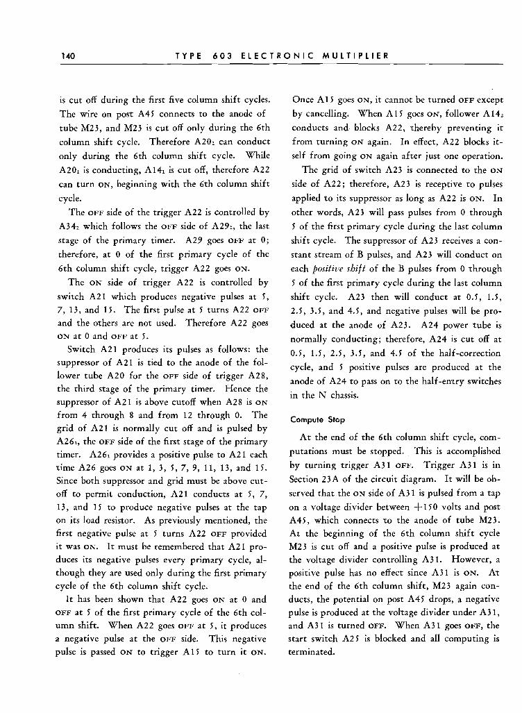
140 T Y P E 6 0 3 E L E C T R O N I C M U L T I P L I E R
is cut off during the first five column shift cycles.
The wire on post A45 connects to the anode of
tube M23, and M23 is cut off only during the 6th
column shift cycle. Therefore A201 can conduct
only during the 6th column shift cycle. While
A201 is conducting, A141 is cut off, therefore A22
can turn ON, beginning with the 6th column shift
cycle.
The OFF side of the trigger A22 is controlled by
A341 which follows the OFF side of A291, the last
stage of the primary timer. A29 goes OFF at 0;
therefore, at O of the first primary cycle of the
6th column shift cycle, trigger A22 goes ON.
The ON side of trigger A22 is controlled by
switch A21 which produces negative pulses at 5,
7, 13, and 15. The first pulse at 5 turns A22 OFF
and the others are not used. Therefore A22 goes
ON at O and OFF at 5.
Switch A21 produces its pulses as follows: the
suppressor of A21 is tied to the anode of the fol-
lower tube A20 for the OFF side of trigger A28,
the third stage of the primary timer. Hence the
suppressor of A21 is above cutoff when A28 is ON
from 4 through 8 and from 12 through 0. The
grid of A21 is normally cut off and is pulsed by
A261, the OFF side of the first stage of the primary
timer. A261 provides a positive pulse to A21 each
rime A26 goes ON at 1, 3, 5, 7, 9, 11, 13, and 15.
Since both suppressor and grid must be above cut-
off to permit conduction, A21 conducts at 5 , 7,
13, and 15 to produce negative pulses at the tap
on its load resistor. As previously mentioned, the
first negative pulse at 5 turns A22 OFF provided
it was ON. I t must be remembered that A21 pro-
duces its negative pulses every primary cycle, al-
though they are used only during the first primary
cycle of the 6th column shift cycle.
It has been shown that A22 goes ON at O and
OFF at 5 of the first primary cycle of the 6th col-
umn shifi. When A22 goes OFF at 5, it produces
a negative pulse at the OFF side. This negative
pulse is passed ON to trigger A15 to turn it ON.
Once A1 5 goes ON, it cannot be turned OFF except
by cancelling. When A1 5 goes ON, follower A142
conducts and blocks A22, thereby preventing it
from turning ON again. In effect, A22 blocks it-
self from going ON again after just one operation.
The grid of switch A23 is connected to the ON
side of A22; therefore, A23 is receptive to pulses
applied to its suppressor as long as A22 is ON. In
other words, A23 will pass pulses from O through
5 of the first primary cycle during the last column
shift cycle. The suppressor of A23 receives a con-
stant stream of B pulses, and A23 will conduct on
each positive shift of the B pulses from 0 through
5 of the first primary cycle during the last column
shift cycle. A23 then will conduct at 0.5, 1.5,
2.5, 3.5, and 4.5, and negative pulses will be pro-
duced at the anode of A23. A24 power tube is
normally conducting; therefore, A24 is cut off at
0.5, 1.5, 2.5, 3.5, and 4.5 of the half-correction
cycle, and 5 positive pulses are produced at the
anode of A24 to pass on to the half-entry switches
in the N chassis.
Compute Stop
A t the end of the 6th column shift cycle, com-
putations must be stopped. This is accomplished
by turning trigger A3 1 OFF. Trigger A31 is in
Section 23A of the circuit diagram. I t will be ob-
served that the ON side of A3 1 is pulsed from a tap
on a voltage divider between +I50 volts and post
A45, which connects t o the anode of tube M23.
At the beginning of the 6th column shift cycle
M23 is cut off and a positive pulse is produced at the voltage divider controlling A31. However, a
positive pulse has no effect since A31 is ON. At
the end of the 6th column shift, M23 again con-
ducts, the potential on post A45 drops, a negative
pulse is produced at the voltage divider under A3 1,
and A3 1 is turned OFF. When A3 1 goes OFF, the
start switch A25 is blocked and all computing is
terminated.

I ELECTRONIC U N I T - y P U N C H UNIT
B Chossls Pulse Control
lndex Line Pulse
C B's Index Mid-~ndex ( Punch)
NarJ I 1 I Choss~s I I W 8 X I I I N Chassis i ~ l ~ p p e r s 1 P.R.S,T,U,Y Cha~a ia I Chassis I Y 8 Z Choseis I I I Input lnwerters, l n ~ ~ r I Product Counter 1 Readout Trigger 1 ~ e a d o u t Inverters Reodout Power Tubes(
-
8-28
Punch Mognol
-
Pulses' to turn Readout T r ~ p g a r r OFF a t Midindax
counter Reading "3"
Pbwer Tuba
Pulses to Product Counter (Punch lndex Lines)
9 8- 7 6 5 4- 3
I 2 1- 0-
4 . 5 6 7 8 9 0 I 2 3 I
Raodout Pulsa
Trigger
Wl thn3"~n Counter, carry occurs here - Couslng Punch Magnet to be energized ond
"3" to be punched
Fidure 126. Block Diagram o f Read-oyt Circuits
8 - 2 9

142 T Y P E 6 0 3 E L E C T R O N l C M U L T I P L I E R
Read-Out Circuits
After the computation is finished, the electronic
unit must wait until the card in which the product
is to be punched reaches the die and stripper. Dur-
ing this cycle the product is read out and punched
in the card, and the product counter is cancelled
shortly after O on the punch index.
Read-out is almost exactly the reverse process to
read-in. When reading into a counter, pulses are
fed t o the counter in synchronism with card move-
ment after reading the hole in the card. When
reading out, pulses are applied to all product
counter positions in synchronism with the card
movement, beginning at 9 on the punch index.
When a carry occurs, a hole is punched.
Figure 126 shows the read-out circuits in block
diagram form. Trigger B29 goes ON and OFF un-
der control of P-cam contacts in the punch unit.
B29 goes ON at index lines and OFF at mid-index
lines. B30 power tube produces positive pulses in
synchronism with card movement through the
punch, beginning at 9. These positive pulses are applied to the grids of the 12 inverters in the N
chassis which in turn provide negative pulses to
feed to the 12 product counter positions. When any ~ r o d u c t counter ~osition goes from 9 to 0,
the corresponding read-out (or carry) trigger goes
ON, and the corresponding read-out inverter is cut
off, thereby producing a positive pulse to cause the
power tubes to conduct and energize a punch mag-
nH. A t the mid-index points, power tube B28
turns OFF any read-out triggers which happen to
be ON and thereby prevents the possibility of
punching two holes in the same column.
The actual circuit for producing the read-out
pulses is shown in Figure 127. Trigger B29 is
turned ON each time P7 and P8 make on the punch
index lines, provided the relay points controlling
the read-out circuit are closed. RI is picked up as long as cards are at the die, and the points of R29
and R19 are closed except when a rate card passes
the die when group multiplying, or when accumu-
lating products for punching in a subsequent card
on a product summary run.
Trigger B29 is turned OFF at mid-index points
each time Py and P6 make, therefore B29 goes ON
at each index line and OFF at mid-index points.
Each time B29 goes ON, a negative pulse is passed
to B30 power tube through the 50 mmfd coupling
capacitor. Since B30 is normally conducting each
time B29 goes ON, B.30 momentarily stops con-
ducting and produces a positive pulse at its anode.
This positive pulse is passed to post N41 and on to
all 12 inverters in the N chassis through the 1000 mmfd capacitor. N21, inverter for the first posi-
tion for the product counter, is shown in Figure
127. The inverters produce -50 volt pulses to pass on the product counter. The lower half of the
load resistors for inverters in the N chassis are
shared with the corresponding column shift
switches. Each product counter position receives a rolling pulse each time B29 goes ON. The .0025
megohm resistors shown connected between gound
and posts B30 and B3 1 serve to maintain a con-
tinuous current flow through the P-cam contacts.
The read-out circuit for the first position of the product counter is shown in Figure 128. When
the first position of the product counter goes from
9 to 0, trigger W I goes ON, and the potential at the anode of tube W 1 2 drops. This drop in poten-
tial drops the grid of Y41 below cutoff, and the potential at the anode of Y41 rises. In turn, the
rise in potential at the anode of Y41 drives the
g ids of Y2 and Y3 power tubes above cutoff. The
0.1 mfd coupling capacitor provides a sufficient
time constanft to insure that Y2 and Y3 will con-
duct long enough to cause a hole to be punched.
Two power tubes are used in parallel to furnish
the current required by a punch magnet. It will be observed that the anode potential sup-
ply for the read-out power tubes is not in the elec-
tronic unit. The +I40 volt supply furnished by
the half-wave selenium rectifier in the punch unit
furnishes power to energize the punch magnets during read-out. The anode potential is applied

E L E C T R I C A L P R I N C I P L E S

1 44 T Y P E 6 0 3 E L E C T R O N I C M U L T I P L I E R
Figure 128. Product Counter Read-out Circuit
only during read-out time by P14 cam contact.
The potential drop across the punch magnet is 40
volts and across the power tubes, 100 volts. I t will
be observed that the cathodes of the power tubes
are not at ground potential because the punch
magnets are connected to ground.
At the mid-index point following the turning
ON of W1 trigger, it is turned OFF by B28 power
tube, as shown in Figure 129. Each time B29 goes
OFF (at mid-index points) a positive pulse passes
to the B28 power tube, which is normally cut off;
B28 momentarily conducts and produces a nega-
tive pulse at the midpoint of its load resistor. This
negative pulse passes to the ON side of all read-out
triggers to turn OFF any that happen to be ON.
This is illustrated in the block diagram of Figure
126.
To P - 7 , P - 0 To P-5.P-6 4 Mob. ol punch mC1 l i n n l (Mob. 01 mid-index l8n.s )
f PUNCH UNIT
--- TO Car,, OVlPYt Prod Counlar Po. I
T
I I .--
-too--. concal
- I 0 0 Concal
Figure 129. Triggering Off o f Read-out Triggers at Mid-Index