electricalandinterfacialpropertiesof -si/p3ht...
TRANSCRIPT

Vol. 120 (2011) ACTA PHYSICA POLONICA A No. 3
Electrical and Interfacial Properties of p-Si/P3HTOrganic-on-Inorganic Junction Barrier
F. Yakuphanoglua,∗, M. Shahb and W. Aslam Farooqc
aPhysics Department, Faculty of Science, Firat University, Elazig, TurkeybGIK Institute of Engineering Science and Technology, Topi, Swabi, Khyber Pakhtunkhwa, 23640, Pakistan
cDepartment of Physics and Astronomy, College of Science, King Saud UniversityRiyadh, Kingdom of Saudi Arabia
(Received February 22, 2011; in final form March 15, 2011)
The electrical characterization of the Al/p-Si/P3HT/Ag organic-on-inorganic diode was done by current–voltage, capacitance–voltage and conductance–voltage methods. The values of ideality factor and barrier heightof the diode were determined from the current–voltage characteristics and found as 2.32 and 0.77 eV, respectively.These values were also determined from Cheung’s functions and Norde’s method due to the non-ideal behaviorof the diode. The electronic parameters obtained from the various methods indicate a good consistency witheach other. The density of interface states for Al/p-Si/P3HT/Ag organic-on-inorganic diode was found to be7.64 × 1010 cm−2 eV−1. The obtained electrical parameters of the Al/p-Si/P3HT/Ag organic-on-inorganic diodeare higher than that of the conventional Ag/p-Si Schottky diodes. This indicates that the electrical properties ofthe silicon Schottky diodes can be controlled using organic interfacial layer.
PACS: 81.07.Pr, 78.40.Me
1. Introduction
The properties of metal/semiconductor (MS) contactsor organic/inorganic semiconductor structures are ofgreat importance for the potential use in electronic andoptoelectronic devices [1–4]. Heterojunctions and theSchottky diodes have been studied by many researchersusing different organic semiconducting materials [5–8].Organic semiconductor devices have attracted great at-tention due to its advantages over inorganic semiconduc-tor which include large variety of molecular and crystalstructure, low material cost, flexibility, low-temperatureprocessing and large area device processing. Therefore,considerable interest of the researchers has been increasedin the fabrication of organic devices by employing variousorganic materials as active layer [9–14]. Among organicmaterials, polymers have mechanical flexibility, and theirthin films can be deposited by spin-casting, drop-casting,dip-coating and printing. In recent years, conductingpolymers become very attractive for various electronicdevices [15–24]. In particular, the easy processabilityand higher field effect mobility of poly(3-hexylthiophene)(P3HT) make it very promising candidate for the devel-opment of future organic electronic devices [25, 26] andorganic-silicon heterostructure diode can be fabricatedusing P3HT organic semiconductor. Thus, our aim is toinvestigate the electrical properties of p-Si/Ag diode bythe insertion of P3HT organic layer between p-Si semi-conductor using forward bias I–V characteristics and
∗ corresponding author; e-mail: [email protected]
impedance spectroscopy measurements and is to com-pare the parameters of the Al/p-Si/P3HT/Ag organic--on-inorganic diode with those of conventional metal/semiconductor diodes.
In present paper, we present the preparation andcharacterization of the Al/p-Si/P3HT/Ag organic-on--inorganic diode.
2. Experimental details
A p-Si wafer with (100) orientation was used as aninorganic semiconductor. The Si-wafer was chemicallycleaned using the RCA cleaning procedure [i.e. a 10 minboil in NH4OH+H2O2+6H2O followed by a 10 min boilin HCl+H2O2+6H2O]. The native oxide on the front sur-face of the silicon was removed in HF:H2O (1:10) solu-tion and finally the wafer was rinsed in deionised waterfor 30 s. The ohmic contact was done by evaporatingAl on the back of the p-Si substrate at 10−5 Torr and itwas treated at 570 C for 5 min in N2 atmosphere. Thesolution of P3HT was prepared in chlorobenzene and thefilm was coated onto p-type silicon substrate using a spincoater at 1000 rpm and then, the film was dried at roomtemperature. The thickness of P3HT layer was deter-mined to be about 100 nm by atomic force microscopy(AFM). Ag metal was formed on P3HT film through ashadow mask in the vacuum system of 10−5 Torr. In thisway, an Al/p-Si/P3HT/Ag organic-on-inorganic diodewas fabricated. The area of circular diode contact was3.14 × 10−2 cm2. The I–V and C–V –f measurementsof the device were performed using a Keithley 4200AFMSemiconductor characterization system. The structural
(558)
Electrical and Interfacial Properties . . . 559
properties of the organic material deposited on p-typesilicon were analyzed by a Park System XE 100E AFM.
3. Results and discussion
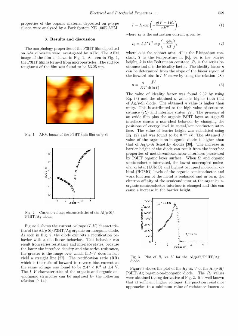
The morphology properties of the P3HT film depositedon p-Si substrate were investigated by AFM. The AFMimage of the film is shown in Fig. 1. As seen in Fig. 1,the P3HT film is formed from microparticles. The surfaceroughness of the film was found to be 53.25 nm.
Fig. 1. AFM image of the P3HT thin film on p-Si.
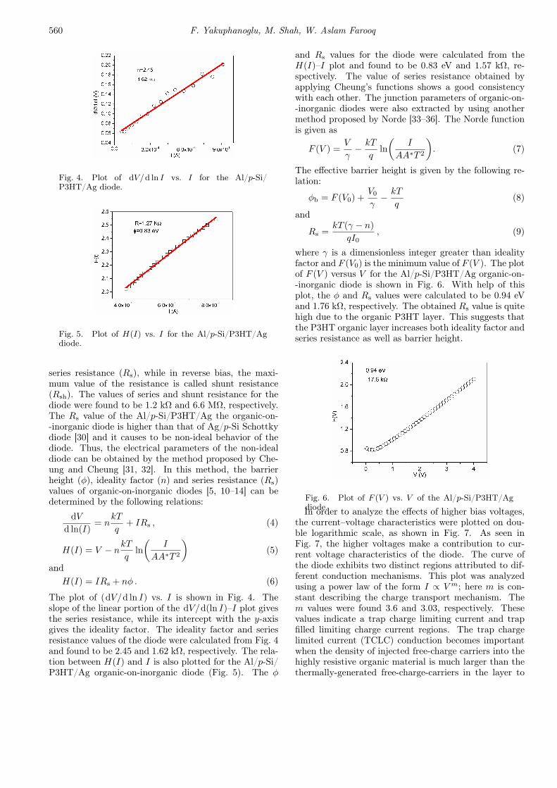
Fig. 2. Current–voltage characteristics of the Al/p-Si/P3HT/Ag diode.
Figure 2 shows the current–voltage (I–V ) characteris-tics of the Al/p-Si/P3HT/Ag organic-on-inorganic diode.As seen in Fig. 2, the diode exhibits a rectification be-havior with a non-linear behavior. This behavior canresult from series resistance and interface states, becausethe lower the interface density and the series resistance,the greater is the range over which ln I–V does in factyield a straight line [27]. The rectification ratio (RR)which is the ratio of forward to reverse bias current atthe same voltage was found to be 2.47 × 10³ at ±4 V.The I–V characteristics of the organic and organic-on--inorganic structures can be analyzed by the followingrelation [9–14]:
I = I0 exp(−q(V − IRs
nkT
), (1)
where I0 is the saturation current given by
I0 = AA∗T 2 exp(−qφb
kT
), (2)
where A is the contact area, A∗ is the Richardson con-stant, T is the temperature in [K], φb is the barrierheight, k is the Boltzmann constant, Rs is the series re-sistance and n is the ideality factor. The ideality factor ncan be determined from the slope of the linear region ofthe forward bias ln I–V curve by using the relation [28]:
n =q
KT
dV
d(ln I). (3)
The value of ideality factor was found 2.32 by usingEq. (3) and the obtained n value is higher than thatof Ag/p-Si diode. The obtained n value is higher thanunity. This is attributed to the high value of series re-sistance (Rs) and interface states [29]. The presence ofan oxide film plus the organic P3HT layer at Ag/p-Siinterface causes a non-ideal behavior by changing thepositions of energy level in metal/semiconductor inter-face. The value of barrier height was calculated usingEq. (2) and was found to be 0.77 eV. The obtained φvalue of the organic-on-inorganic diode is higher thanthat of Ag/p-Si Schottky diodes [30]. The increase inbarrier height of the diode can result from the interfaceproperties of metal/semiconductor interfaces passivatedby P3HT organic layer surface. When Si and organicsemiconductor interacted, the lowest unoccupied molec-ular orbital (LUMO) and highest occupied molecular or-bital (HOMO) levels of the organic semiconductor andwork function of the metal is realigned and in turn, theelectron affinity of the semiconductor at the organic/in-organic semiconductor interface is changed and this cancause a increase in the barrier height.
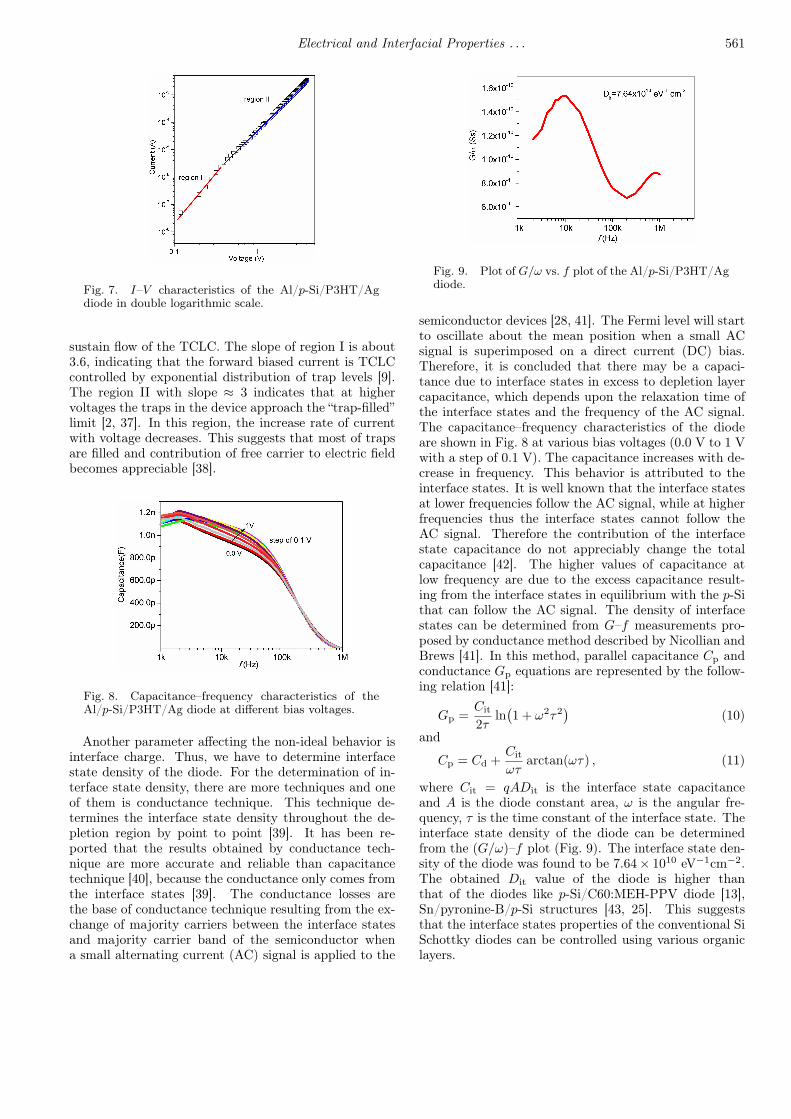
Fig. 3. Plot of Rj vs. V for the Al/p-Si/P3HT/Agdiode.
Figure 3 shows the plot of the Rj vs. V of the Al/p-Si/P3HT/Ag organic-on-inorganic diode. The Rj valueswere obtained taking derivative of Fig. 2. It is well knownthat at sufficient higher voltages, the junction resistanceapproaches to a minimum value of resistance known as
560 F. Yakuphanoglu, M. Shah, W. Aslam Farooq
Fig. 4. Plot of dV/d ln I vs. I for the Al/p-Si/P3HT/Ag diode.
Fig. 5. Plot of H(I) vs. I for the Al/p-Si/P3HT/Agdiode.
series resistance (Rs), while in reverse bias, the maxi-mum value of the resistance is called shunt resistance(Rsh). The values of series and shunt resistance for thediode were found to be 1.2 kΩ and 6.6 MΩ, respectively.The Rs value of the Al/p-Si/P3HT/Ag the organic-on--inorganic diode is higher than that of Ag/p-Si Schottkydiode [30] and it causes to be non-ideal behavior of thediode. Thus, the electrical parameters of the non-idealdiode can be obtained by the method proposed by Che-ung and Cheung [31, 32]. In this method, the barrierheight (φ), ideality factor (n) and series resistance (Rs)values of organic-on-inorganic diodes [5, 10–14] can bedetermined by the following relations:
dV
d ln(I)= n
kT
q+ IRs , (4)
H(I) = V − nkT
qln
(I
AA∗T 2
)(5)
andH(I) = IRs + nφ . (6)
The plot of (dV/d ln I) vs. I is shown in Fig. 4. Theslope of the linear portion of the dV/d(ln I)–I plot givesthe series resistance, while its intercept with the y-axisgives the ideality factor. The ideality factor and seriesresistance values of the diode were calculated from Fig. 4and found to be 2.45 and 1.62 kΩ, respectively. The rela-tion between H(I) and I is also plotted for the Al/p-Si/P3HT/Ag organic-on-inorganic diode (Fig. 5). The φ
and Rs values for the diode were calculated from theH(I)–I plot and found to be 0.83 eV and 1.57 kΩ, re-spectively. The value of series resistance obtained byapplying Cheung’s functions shows a good consistencywith each other. The junction parameters of organic-on--inorganic diodes were also extracted by using anothermethod proposed by Norde [33–36]. The Norde functionis given as
F (V ) =V
γ− kT
qln
(I
AA∗T 2
). (7)
The effective barrier height is given by the following re-lation:
φb = F (V0) +V0
γ− kT
q(8)
and
Rs =kT (γ − n)
qI0, (9)
where γ is a dimensionless integer greater than idealityfactor and F (V0) is the minimum value of F (V ). The plotof F (V ) versus V for the Al/p-Si/P3HT/Ag organic-on--inorganic diode is shown in Fig. 6. With help of thisplot, the φ and Rs values were calculated to be 0.94 eVand 1.76 kΩ, respectively. The obtained Rs value is quitehigh due to the organic P3HT layer. This suggests thatthe P3HT organic layer increases both ideality factor andseries resistance as well as barrier height.
Fig. 6. Plot of F (V ) vs. V of the Al/p-Si/P3HT/Agdiode.In order to analyze the effects of higher bias voltages,
the current–voltage characteristics were plotted on dou-ble logarithmic scale, as shown in Fig. 7. As seen inFig. 7, the higher voltages make a contribution to cur-rent voltage characteristics of the diode. The curve ofthe diode exhibits two distinct regions attributed to dif-ferent conduction mechanisms. This plot was analyzedusing a power law of the form I ∝ V m; here m is con-stant describing the charge transport mechanism. Them values were found 3.6 and 3.03, respectively. Thesevalues indicate a trap charge limiting current and trapfilled limiting charge current regions. The trap chargelimited current (TCLC) conduction becomes importantwhen the density of injected free-charge carriers into thehighly resistive organic material is much larger than thethermally-generated free-charge-carriers in the layer to
Electrical and Interfacial Properties . . . 561
Fig. 7. I–V characteristics of the Al/p-Si/P3HT/Agdiode in double logarithmic scale.
sustain flow of the TCLC. The slope of region I is about3.6, indicating that the forward biased current is TCLCcontrolled by exponential distribution of trap levels [9].The region II with slope ≈ 3 indicates that at highervoltages the traps in the device approach the “trap-filled”limit [2, 37]. In this region, the increase rate of currentwith voltage decreases. This suggests that most of trapsare filled and contribution of free carrier to electric fieldbecomes appreciable [38].
Fig. 8. Capacitance–frequency characteristics of theAl/p-Si/P3HT/Ag diode at different bias voltages.
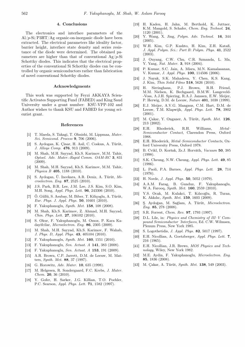
Another parameter affecting the non-ideal behavior isinterface charge. Thus, we have to determine interfacestate density of the diode. For the determination of in-terface state density, there are more techniques and oneof them is conductance technique. This technique de-termines the interface state density throughout the de-pletion region by point to point [39]. It has been re-ported that the results obtained by conductance tech-nique are more accurate and reliable than capacitancetechnique [40], because the conductance only comes fromthe interface states [39]. The conductance losses arethe base of conductance technique resulting from the ex-change of majority carriers between the interface statesand majority carrier band of the semiconductor whena small alternating current (AC) signal is applied to the
Fig. 9. Plot of G/ω vs. f plot of the Al/p-Si/P3HT/Agdiode.
semiconductor devices [28, 41]. The Fermi level will startto oscillate about the mean position when a small ACsignal is superimposed on a direct current (DC) bias.Therefore, it is concluded that there may be a capaci-tance due to interface states in excess to depletion layercapacitance, which depends upon the relaxation time ofthe interface states and the frequency of the AC signal.The capacitance–frequency characteristics of the diodeare shown in Fig. 8 at various bias voltages (0.0 V to 1 Vwith a step of 0.1 V). The capacitance increases with de-crease in frequency. This behavior is attributed to theinterface states. It is well known that the interface statesat lower frequencies follow the AC signal, while at higherfrequencies thus the interface states cannot follow theAC signal. Therefore the contribution of the interfacestate capacitance do not appreciably change the totalcapacitance [42]. The higher values of capacitance atlow frequency are due to the excess capacitance result-ing from the interface states in equilibrium with the p-Sithat can follow the AC signal. The density of interfacestates can be determined from G–f measurements pro-posed by conductance method described by Nicollian andBrews [41]. In this method, parallel capacitance Cp andconductance Gp equations are represented by the follow-ing relation [41]:
Gp =Cit
2τln
(1 + ω2τ2
)(10)
and
Cp = Cd +Cit
ωτarctan(ωτ) , (11)
where Cit = qADit is the interface state capacitanceand A is the diode constant area, ω is the angular fre-quency, τ is the time constant of the interface state. Theinterface state density of the diode can be determinedfrom the (G/ω)–f plot (Fig. 9). The interface state den-sity of the diode was found to be 7.64× 10¹⁰ eV−1cm−2.The obtained Dit value of the diode is higher thanthat of the diodes like p-Si/C60:MEH-PPV diode [13],Sn/pyronine-B/p-Si structures [43, 25]. This suggeststhat the interface states properties of the conventional SiSchottky diodes can be controlled using various organiclayers.
562 F. Yakuphanoglu, M. Shah, W. Aslam Farooq
4. Conclusions
The electronics and interface parameters of theAl/p-Si/P3HT/Ag organic-on-inorganic diode have beenextracted. The electrical parameters like ideality factor,barrier height, interface state density and series resis-tance of the diode were determined. The obtained pa-rameters are higher than that of conventional Ag/p-SiSchottky diodes. This indicates that the electrical prop-erties of the conventional Si Schottky diodes can be con-trolled by organic semiconductors rather than fabricationof novel conventional Schottky diodes.
Acknowledgments
This work was supported by Feyzi AKKAYA Scien-tific Activates Supporting Fund (FABED) and King SaudUniversity under a grant number: KSU-VPP-102 andAuthor wishes to thank KSU and FABED for young sci-entist grant.
References
[1] T. Maeda, S. Takagi, T. Ohnishi, M. Lippmaa, Mater.Sci. Semicond. Process 9, 706 (2006).
[2] S. Aydogan, K. Çinar, H. Asil, C. Coskun, A. Türüt,J. Alloys Comp. 476, 913 (2009).
[3] M. Shah, M.H. Sayyad, Kh.S. Karimov, M.M. Tahir,Optoel. Adv. Mater.-Rapid Comm. OAM-RC 3, 831(2009).
[4] M. Shah, M.H. Sayyad, Kh.S. Karimov, M.M. Tahir,Physica B 405, 1188 (2010).
[5] S. Aydogan, Ü. Incekara, A.R. Deniz, A. Türüt, Mi-croelectron. Eng. 87, 2525 (2010).
[6] J.S. Park, B.R. Lee, J.M. Lee, J.S. Kim, S.O. Kim,M.H. Song, Appl. Phys. Lett. 96, 243306 (2010).
[7] Ö. Güllü, S. Asubay, M. Biber, T. Kiliçoglu, A. Türüt,Eur. Phys. J. Appl. Phys. 50, 10401 (2010).
[8] F. Yakuphanoglu, Synth. Met. 158, 108 (2008).[9] M. Shah, Kh.S. Karimov, Z. Ahmad, M.H. Sayyad,
Chin. Phys. Lett. 27, 106102 (2010).[10] S. Okur, F. Yakuphanoglu, M. Ozsoz, P. Kara Ka-
dayifcilar, Microelectron. Eng. 86, 2305 (2009).[11] M. Shah, M.H. Sayyad, Kh.S. Karimov, F. Wahab,
J. Phys. D, Appl. Phys. 43, 405104 (2010).[12] F. Yakuphanoglu, Synth. Met. 160, 1551 (2010).[13] F. Yakuphanoglu, Sen. Actuat. A 141, 383 (2008).[14] F. Yakuphanoglu, Sen. Actuat. A 153, 191 (2009).[15] A.R. Brown, C.P. Jarrett, D.M. de Leeuw, M. Mat-
ters, Synth. Met. 88, 37 (1997).[16] G. Horowitz, Adv. Mater. 10, 635 (1998).[17] M. Helgesen, R. Sondergaard, F.C. Krebs, J. Mater.
Chem. 20, 36 (2010).[18] Y. Gofer, H. Sarker, J.G. Killian, T.O. Poehler,
P.C. Searson, Appl. Phys. Lett. 71, 1582 (1997).
[19] H. Kaden, H. Jahn, M. Berthold, K. Juttner,K.M. Mangold, S. Schafer, Chem. Eng. Technol. 24,1120 (2001).
[20] Y. Wang, X. Jing, Polym. Adv. Technol. 16, 344(2005).
[21] W.H. Kim, G.P. Kushto, H. Kim, Z.H. Katafi,J. Appl. Polym. Sci.: Part B: Polym. Phys. 41, 2522(2003).
[22] J. Ouyang, C.W. Chu, C.R. Szmanda, L. Ma,Y. Yang, Nat. Mater. 3, 918 (2004).
[23] P. Kumar, S.C. Jain, A. Misra, M.N. Kamalasanan,V. Kumar, J. Appl. Phys. 100, 114506 (2006).
[24] J. Nayak, S.K. Mahadeva, Y. Chen, K.S. Kang,J. Kim, Thin Solid Films 518, 5626 (2010).
[25] H. Sirringhaus, P.J. Brown, R.H. Friend,M.M. Nielsen, K. Bechgaard, B.M.W. Langeveld--Voss, A.J.H. Spiering, R.A.J. Janssen, E.W. Meijer,P. Herwig, D.M. de Leeuw, Nature 401, 1038 (1999).
[26] E.J. Meijer, A.V.G. Mangnus, C.M. Hart, D.M. deLeeuw, T.M. Klapwijk, Appl. Phys. Lett. 78, 3902(2001).
[27] M. Çakar, Y. Onganer, A. Türüt, Synth. Met. 126,213 (2002).
[28] E.H. Rhoderick, R.H. Williams, Metal–Semiconductor Contact, Clarendon Press, Oxford1988.
[29] E.H. Rhoderick, Metal–Semiconductor Contacts, Ox-ford University Press, Oxford 1978.
[30] B. Cvikl, D. Koršak, Zs.J. Horváth, Vacuum 50, 385(1998).
[31] S.K. Cheung, N.W. Cheung, Appl. Phys. Lett. 49, 85(1986).
[32] L. Paoli, P.A. Barnes, Appl. Phys. Lett. 28, 714(1976).
[33] H. Norde, J. Appl. Phys. 50, 5052 (1979).[34] A.A.M. Farag, B. Gunduz, F. Yakuphanoglu,
W.A. Farooq, Synth. Met. 160, 2559 (2010).[35] Y.S. Ocak, M. Kulakci, T. Kılıcoğlu, R. Turan,
K. Akkılıc, Synth. Met. 159, 1603 (2009).[36] Ş. Aydoğan, M. Sağlam, A. Türüt, Microelectron.
Eng. 85, 278 (2008).[37] S.R. Forrest, Chem. Rev. 97, 1793 (1997).[38] D.L. Lile, in: Physics and Chemistry of III–V Com-
pound Semiconductor ˙Interfaces, Ed. C.W. Wilmsen,Plenum Press, New York 1985.
[39] S. Logothetidis, J. Appl. Phys. 82, 5017 (1997).[40] E.H. Nicollian, A. Goetzberger, Appl. Phys. Lett. 7,
216 (1965).[41] E.H. Nicollian, J.R. Brews, MOS Physics and Tech-
nology, Wiley, New York 1982.[42] M.E. Aydin, F. Yakuphanoglu, Microelectron. Eng.
85, 1836 (2008).[43] M. Çakar, A. Türüt, Synth. Met. 138, 549 (2003).