electrochemical deposition of sers active nanostructured silver films
TRANSCRIPT
Int. J. Electrochem. Sci., 8 (2013) 80 - 99
International Journal of
ELECTROCHEMICAL SCIENCE
www.electrochemsci.org
Electrochemical deposition of SERS active nanostructured silver
films
Renáta Oriňáková1*
, Lenka Škantárová2, Andrej Oriňák
1, Jakub Demko
1, Miriam Kupková
3, Jan T.
Andersson4
1
Department of Physical Chemistry, Faculty of Science, P.J. Šafárik University, Moyzesova 11,
SK-04154 Košice, Slovak Republic, European Union 2 Department of Analytical Chemistry, Faculty of Science, Comenius University, Mlynská Dolina,
SK-842 15 Bratislava 4, Slovak Republic, European Union 3 Institute of Materials Research, Slovak Academy of Science, Watsonova 47, SK-04353 Košice,
Slovak Republic, European Union
4 Institute of Inorganic and Analytical Chemistry, University of Münster, Correnstrasse 30, D-48149
Münster, Germany, European Union *
E-mail: [email protected]
Received: 31 July 2012 / Accepted: 31 August 2012 / Published: 1 January 2013
An electrochemical multiple scan cyclic voltammetry (CV) method was used to prepare surface-
enhanced Raman scattering (SERS) active silver island films to investigate the effect of potential scan
rate and number of CV scans on the SERS performance. The SERS enhancement capability is particle
size and distribution as well surface profile amplitude dependent with an optimal potential scan rate of
100 mV/s and 30 CV scans at the experimental conditions used. Scanning electron microscopy and
optical profilometry investigation reveal that the highest SERS effect was associated with the
homogenously distributed uniform size aggregates merged to interconnecting network. The
enhancement factor for Rhodamine 6G (R6G) adsorbed on the SERS-active Ag film was estimated to
be 3.7×10¹²
and a detection limit of about 5×10⁻¹⁶
mol/l was reached.
Keywords: Electrochemical Deposition, Cyclic Voltammetry, Surface-Enhanced Raman Scattering,
Ag Island Films, Enhancement Factor
1. INTRODUCTION
The technique of surface enhanced Raman spectroscopy (SERS) is a particularly sensitive and
selective analytical tool for the detection of low-concentrations of analytes adsorbed on noble metal
nanostructures [1-5], sometimes even achieving single-molecule sensitivity [2, 6, 7]. SERS occurring
Int. J. Electrochem. Sci., Vol. 8, 2013
81
on nanostructured metallic surfaces provides a powerful means of obtaining vibrational information on
adsorbate–surface interactions in view of its unique sensitivity and excellent frequency resolution from
the large increase in scattering [3-5, 7-9]. The detection of single molecules elevated SERS to the very
restricted group of techniques able to attain this ultimate limit of detection and gave a new direction to
the SERS research field [7]. SERS is widely applied to the study of the structure and orientation of
molecules at Cu, Ag and Au surfaces [1, 10]. The surface enhancement is highly surface selective so
the technique is sensitive to molecules adsorbed at, or very close to the substrate surface. Moreover,
the Raman cross section for water is low so that SERS can be easily used to study substrates in
aqueous solution [1]. SERS has grown to become a very active field of research in several areas of
materials and analytical sciences [7].
The mechanism of SERS, as it is now widely accepted, consists of two major components
contributing to the overall SERS effect: electromagnetic (EM) and chemical (CHEM) enhancement [3-
5, 10-12]. The former arises from the enhancement of the electromagnetic field at the analyte location
due to the occurrence of localized surface plasmon resonance (LSPR) [3, 4, 7, 11]. The local field can
be enhanced to a far greater extent when neighbouring nanofeatures interact with each other over
distances in the order of 1–2 nm [7, 13]. The regions of highly enhanced local electromagnetic fields
are called “SERS hot spots”. CHEM enhancement takes place only if molecules are in contact with the
surface directly, and it is associated with the charge transfer between the metal and adsorbate at
atomic-scale roughness features [3-5, 11]. The most common of the chemical models assume the
appearance of new electronic states due to chemisorption [7]. This is poorly understood in comparison
to the EM enhancement [4, 5]. Of these two the EM contribution is usually the more significant and is
not adsorbate specific [1, 12]. The magnitude of the EM enhancement is highly dependent on the
surface morphology and the precise shape of the roughness features at the metal surface as well on the
plasmon absorption of the SERS substrate [1, 7, 10, 12, 14].
An average value for the SERS enhancement is around 106 but the localized enhancement may
reach peaks of 1010
at certain highly efficient sub-wavelength regions of the surface [7]. The
generation and intensity of Raman signals are determined by the surface morphology and structure of
the substrates [1, 7, 8, 12]. Thus, considerable efforts have been directed toward the optimization of
SERS enhancement via the size- and shape-controlled physical and chemical properties of the SERS
active substrates [12]. One of the major challenges in the field of SERS is the difficulty in producing
efficient SERS substrates with good stability, at low cost and high enhancement factors, with
reproducibility and uniformity over the whole substrate. It is also desirable that the substrates are easy
to fabricate and store [2, 3, 9].
The original substrates for SERS were electrochemically roughened metal electrodes [7, 15,
16]. Currently, there are many kinds of SERS-active substrates used in a wide range of SERS
applications. These include the use of grating structures [17], colloidal particle arrays [18, 19], and
geometrically structured metal surfaces [20]. Of special interest is the synthesis of noble-metal (Au,
Ag and Cu) nanoparticle patterns with controllable particle size and shape, because such nanoparticle
patterns offer the possibility of developing various functional devices with optical, sensing, and
electrical properties [6, 7, 11, 12].
Int. J. Electrochem. Sci., Vol. 8, 2013
82
In preparing metal island films on substrates for SERS studies, various techniques have been
developed. They include electron beam lithography [21], microcontact printing [22], sputtering coating
[23], vacuum evaporation deposition [24], self-assembly [25], laser deposition [26], electrochemical
deposition [27], chemically etching methods [28], and so on. Recent investigations have highlighted
electrodeposition as an attractive approach for the preparation of nanostructured materials.
Electrodeposition, which does not require complex equipment, provides a cost-effective method for the
preparation of nanocrystalline and nanophase metallic materials either as coatings or as freestanding
objects even in complex shapes (foils, wires, electroforms). The low processing temperature minimizes
interdiffusion or chemical reaction. The film thickness can be accurately controlled by monitoring the
consumed charge. Composition and defect chemistry can be controlled by electrical and fluid-dynamic
means. Deposition rates of the order of several tens of microns per hour can be routinely achieved [29,
30]. A controllable and reproducible surface roughness can be generated through control of the
electrochemical oxidation–reduction cycles procedure [4, 5].
It has been established that metallic silver is an excellent material for SERS [3, 5, 6, 8-10, 15,
17, 25, 31]. Ag arrayed nanostructure has been extensively studied and become one of the best
established systems [3, 10, 32]. Recently, SERS effects of various nanostructures, for example, Ag
nanowire bundles [8], Ag nanorod arrays [10, 14], Ag dendritic structures [31, 33], flowerlike Ag
nanostructures [34] and nanoparticles [12, 32] were reported.
In this work, the silver island films were produced using electrodeposition onto stainless steel
substrates by cyclic voltammetry (CV). The morphology of substrates was changed through tuning the
scan rate of the applied potential and the number of scans. The Raman scattering enhancement
efficiency of the prepared surfaces was investigated by SERS measurements of Rhodamine 6G (R6G)
as a reference molecule. The textural and topographical properties of the Ag nanoparticle substrate
were correlated with the corresponding enhancement factor to determine the factors that could improve
the design of Ag nanoparticle SERS active substrates.
2. EXPERIMENTAL PART
2.1. Electrochemical deposition of Ag island films
Silver island films were electrochemically synthesized by multiple scan CV using an
electrolyte containing 0.1 mol/l KNO3, 0.1 mol/l KCN and 0.01 mol/l AgNO3 (pH = 10.25) in a
conventional three-electrode cell controlled by an Autolab PGSTAT302N (Metrohm) at room
temperature. A sheet of stainless steel with a bare surface area of 1 cm2, a 0.56 cm
2 platinum sheet, and
an Ag/AgCl/3 mol/l KCl electrode were employed as the working, counter and reference electrodes,
respectively. The working electrode was typically cycled for 10 – 40 cycles between –700 and
–1550 mV (vs. Ag/AgCl/3 mol/l KCl), beginning at –700 mV, with scan rate 50 – 250 mV/s in order
to affect electrodeposition. The electrolyte solution was degassed by nitrogen purging.
Int. J. Electrochem. Sci., Vol. 8, 2013
83
2.2 Surface morphology of Ag island films
The morphology of the samples was characterized ex situ using a scanning electron microscope
JEOL JSM-7000F (Japan). To better illustrate the surface topography, an optical confocal profilometer
Plu NeoX (Sensofar, Spain) was used.
The particle size distribution histogram for each sample was calculated by analyzing 300 - 500
particles from SEM images taken at different regions of the sample in order to obtain particle Feret's
diameter (also known as the caliper length).
2.3. SERS analysis of Ag island films
Raman spectra were obtained using an i-Raman® instrument (B&W Tek). Excitation was
provided by a 532.1-nm Nd:YAG laser. The laser power at the sample was approximately 9 mW. The
acquisition time for each accumulation was 5 s.
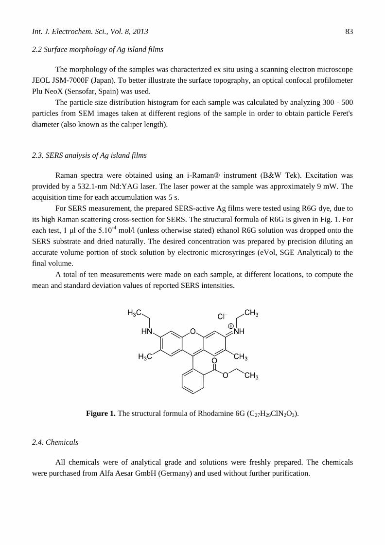
For SERS measurement, the prepared SERS-active Ag films were tested using R6G dye, due to
its high Raman scattering cross-section for SERS. The structural formula of R6G is given in Fig. 1. For
each test, 1 μl of the 5.10-4
mol/l (unless otherwise stated) ethanol R6G solution was dropped onto the
SERS substrate and dried naturally. The desired concentration was prepared by precision diluting an
accurate volume portion of stock solution by electronic microsyringes (eVol, SGE Analytical) to the
final volume.
A total of ten measurements were made on each sample, at different locations, to compute the
mean and standard deviation values of reported SERS intensities.
Figure 1. The structural formula of Rhodamine 6G (C27H29ClN2O3).
2.4. Chemicals
All chemicals were of analytical grade and solutions were freshly prepared. The chemicals
were purchased from Alfa Aesar GmbH (Germany) and used without further purification.
Int. J. Electrochem. Sci., Vol. 8, 2013
84
3. RESULTS AND DISCUSSION
3.1. Preparation of Ag island films
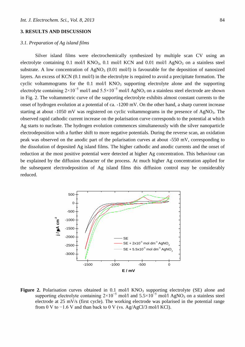
Silver island films were electrochemically synthesized by multiple scan CV using an
electrolyte containing 0.1 mol/l KNO3, 0.1 mol/l KCN and 0.01 mol/l AgNO3 on a stainless steel
substrate. A low concentration of AgNO3 (0.01 mol/l) is favourable for the deposition of nanosized
layers. An excess of KCN (0.1 mol/l) in the electrolyte is required to avoid a precipitate formation. The
cyclic voltammograms for the 0.1 mol/l KNO3 supporting electrolyte alone and the supporting
electrolyte containing 2×10⁻⁵
mol/l and 5.5×10⁻⁵
mol/l AgNO3 on a stainless steel electrode are shown
in Fig. 2. The voltammetric curve of the supporting electrolyte exhibits almost constant currents to the
onset of hydrogen evolution at a potential of ca. -1200 mV. On the other hand, a sharp current increase
starting at about -1050 mV was registered on cyclic voltammograms in the presence of AgNO3. The
observed rapid cathodic current increase on the polarisation curve corresponds to the potential at which
Ag starts to nucleate. The hydrogen evolution commences simultaneously with the silver nanoparticle
electrodeposition with a further shift to more negative potentials. During the reverse scan, an oxidation
peak was observed on the anodic part of the polarisation curves at about -550 mV, corresponding to
the dissolution of deposited Ag island films. The higher cathodic and anodic currents and the onset of
reduction at the most positive potential were detected at higher Ag concentration. This behaviour can
be explained by the diffusion character of the process. At much higher Ag concentration applied for
the subsequent electrodeposition of Ag island films this diffusion control may be considerably
reduced.
-1500 -1000 -500 0
-3000
-2500
-2000
-1500
-1000
-500
0
500
SE
SE + 2x10⁻⁵ mol dm
-3 AgNO
3
SE + 5.5x10⁻⁵ mol dm
-3 AgNO
3
j / A
cm
-2
E / mV
Figure 2. Polarisation curves obtained in 0.1 mol/l KNO3 supporting electrolyte (SE) alone and
supporting electrolyte containing 2×10⁻⁵
mol/l and 5.5×10⁻⁵
mol/l AgNO3 on a stainless steel
electrode at 25 mV/s (first cycle). The working electrode was polarised in the potential range
from 0 V to −1.6 V and than back to 0 V (vs. Ag/AgCl/3 mol/l KCl).
Int. J. Electrochem. Sci., Vol. 8, 2013
85
From these measurements, the desired range of the deposition potential was selected between
-700 mV and -1550 mV to involve an initial cathodic deposition step during which Ag nanoparticles
are formed onto the working electrode as well a subsequent short anodic dissolution step during which
the deposited Ag nanoparticles are partially dissolved. The morphology of substrates was affected by
the scan rate of the applied potential and the number of scans.
3.2. Characterisation of Ag island films
Effect of CV scan number. The morphology of silver structures electrodeposited onto a stainless
steel working electrode was found to be highly dependent on the number of applied CV scans. Figures
3(a) – (g) show the SEM images of the Ag island films deposited after 10, 15, 20, 25, 30, 35 and 40
CV scans, respectively. These images are representative of many images taken at different regions of
the substrate and at a number of magnifications. The surface of the working electrode is decorated with
spherical silver nanoparticles and clusters with varying size distributions (ca. 90 – 500 nm in diameter)
which consist of aggregated smaller crystallites. Lower magnification images revealed the nanoparticle
and cluster beads like arrays. Both the size and the density of the Ag nanoparticles increased with
increasing number of deposition cycles (to ca. 900 nm in diameter). When the number of CV scans is
increased to 35 and 40, the tendency of nanoparticles to coalesce become more pronounced and the
formation of tighter and larger rod-like structures (of ca. 1.5 m wide and 4.5 m long) is favored over
smaller more discrete chain structures.
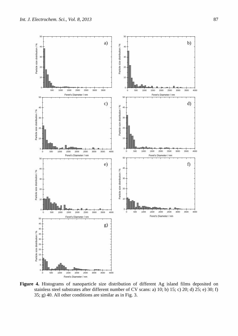
Particle size distribution histograms (Fig. 4) were calculated from the respective SEM images.
The Feret's diameter, expressing the longest distance between any two points along the particle or
aggregate, increased with increasing number of CV scans. At lower CV scan number (Figs. 4(a) - (d)),
particles with the Feret's diameter less than 500 nm predominated but at higher numbers (Figs. 4(e) -
(g)) the fraction of small particles decreased and the amount of larger particles (over 2 m) increased.
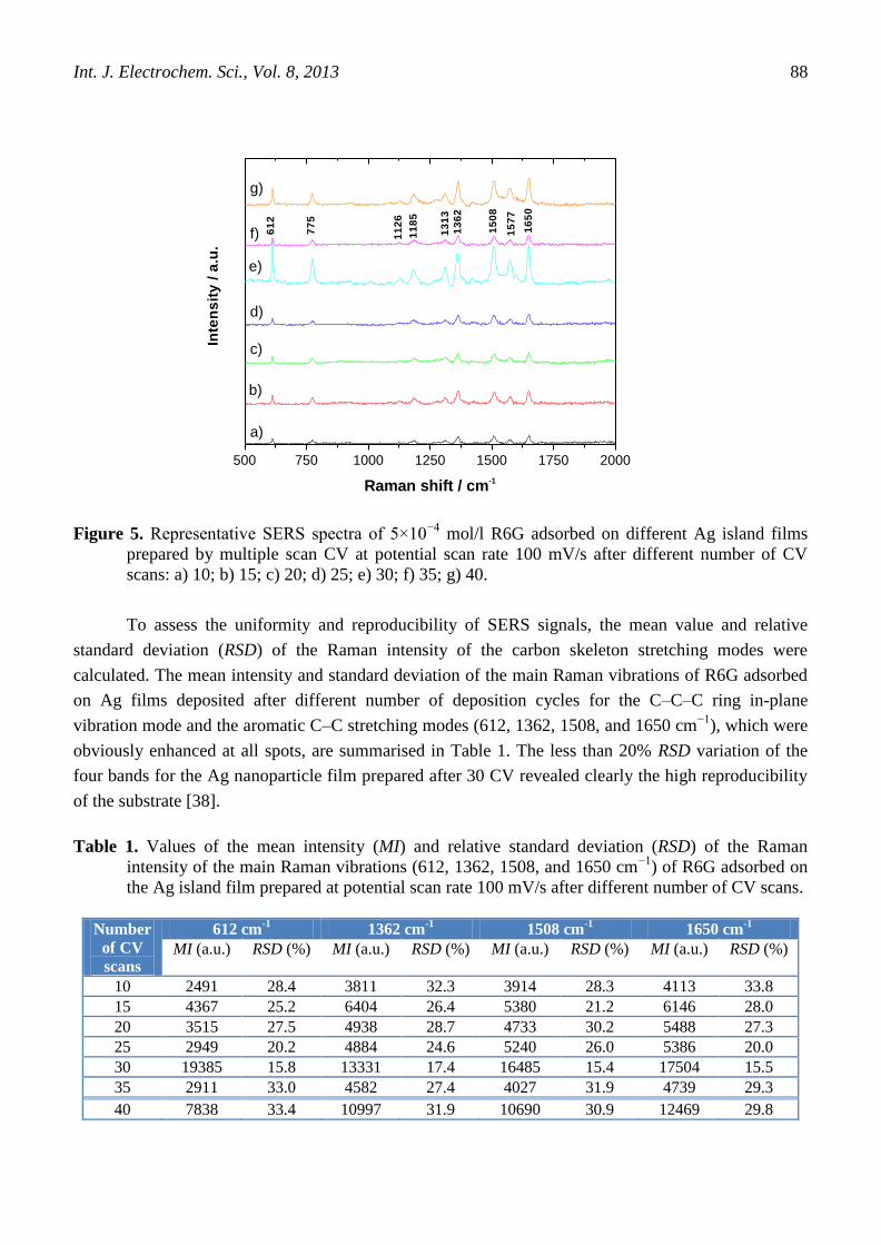
Fig. 5 demonstrates the effect of the applied CV scan number for electrochemical deposition of
silver structures on stainless steel substrates by multiple scan CV method on the corresponding SERS
performance at a potential scan rate of 100 mV/s. The peaks are characteristics of R6G in a Raman
spectrum. The peak at ca. 612 cm−1
is assigned to the C–C–C ring in-plane vibration mode. The peak
at ca. 775 cm−1
is assigned to the C–H out-of-plane bend mode. The peaks at ca. 1126 and 1185 cm−1
are assigned to the C–H in-plane bend mode. The peaks at ca. 1313 and 1577 cm−1
are assigned to the
N–H in-plane bend modes. The peaks at ca. 1362, 1508 and 1650 cm−1
are assigned to the C–C
aromatic stretching vibrations of R6G molecule [4, 5, 35 - 37].
The spectra (a–g) in Fig. 5 show that the optimum number of CV scans for obtaining the
strongest SERS effect at fixed potential scan rate is 30 (spectrum e). The SERS spectrum of R6G
adsorbed on the Ag nanoparticle film prepared after 30 CV scans exhibits approximately 5 times
higher intensity of the strongest peak in the Raman spectrum (at 612 cm-1
) than that of R6G adsorbed
on the other Ag films (Table 1). The Raman intensity decrease for large number of CV scans (>30)
may be due to the aggregation state of Ag nanoparticles is not very capable of creating a great deal of
SERS-active ‘‘hot spots’’.

Int. J. Electrochem. Sci., Vol. 8, 2013
86
Figure 3. Representative SEM images of different Ag island films deposited on stainless steel
substrates by multiple scan CV using an electrolyte containing 0.1 mol/l KNO3, 0.1 mol/l KCN
and 0.01 mol/l AgNO3 between −700 mV and −1550 mV (vs. Ag/AgCl/3 mol/l KCl) at
potential scan rate 100 mV/s after different number of CV scans: a) 10; b) 15; c) 20; d) 25; e)
30; f) 35; g) 40.
a) b)
g)
e)
c)
f)
d)
Int. J. Electrochem. Sci., Vol. 8, 2013
87
Figure 4. Histograms of nanoparticle size distribution of different Ag island films deposited on
stainless steel substrates after different number of CV scans: a) 10; b) 15; c) 20; d) 25; e) 30; f)
35; g) 40. All other conditions are similar as in Fig. 3.
0 500 1000 1500 2000 2500 3000 3500 4000
0
10
20
30
40
50
Pa
rtic
le s
ize
dis
trib
utio
n / %
Feret's Diameter / nm
0 500 1000 1500 2000 2500 3000 3500 4000
0
10
20
30
40
50
P
art
icle
siz
e d
istr
ibu
tio
n / %
Feret's Diameter / nm
500 1000 1500 2000 2500 3000 3500
0
10
20
30
40
50
P
art
icle
siz
e d
istr
ibu
tio
n / %
Feret's Diameter / nm
0 500 1000 1500 2000 2500 3000 3500 4000
0
10
20
30
40
50
P
art
icle
siz
e d
istr
ibu
tio
n / %
Feret's Diameter / nm
0 500 1000 1500 2000 2500 3000 3500 4000
0
10
20
30
40
50
P
art
icle
siz
e d
istr
ibu
tio
n / %
Feret's Diameter / nm
0 500 1000 1500 2000 2500 3000 3500 4000
0
10
20
30
40
50
P
art
icle
siz
e d
istr
ibu
tio
n / %
Feret's Diameter / nm
0 500 1000 1500 2000 2500 3000 3500 4000
0
5
10
15
20
25
30
35
40
45
50
P
art
icle
siz
e d
istr
ibu
tio
n / %
Feret's Diameter / nm
a) b)
g)
e)
c)
f)
d)
Int. J. Electrochem. Sci., Vol. 8, 2013
88
500 750 1000 1250 1500 1750 2000
16
50
15
77
15
08
13
62
13
13
11
85
11
26
77
5
g)
f)
e)
d)
c)
b)
a)
Inte
ns
ity
/ a
.u.
Raman shift / cm-1
61
2
Figure 5. Representative SERS spectra of 5×10
−4 mol/l R6G adsorbed on different Ag island films
prepared by multiple scan CV at potential scan rate 100 mV/s after different number of CV
scans: a) 10; b) 15; c) 20; d) 25; e) 30; f) 35; g) 40.
To assess the uniformity and reproducibility of SERS signals, the mean value and relative
standard deviation (RSD) of the Raman intensity of the carbon skeleton stretching modes were
calculated. The mean intensity and standard deviation of the main Raman vibrations of R6G adsorbed
on Ag films deposited after different number of deposition cycles for the C–C–C ring in-plane
vibration mode and the aromatic C–C stretching modes (612, 1362, 1508, and 1650 cm−1
), which were
obviously enhanced at all spots, are summarised in Table 1. The less than 20% RSD variation of the
four bands for the Ag nanoparticle film prepared after 30 CV revealed clearly the high reproducibility
of the substrate [38].
Table 1. Values of the mean intensity (MI) and relative standard deviation (RSD) of the Raman
intensity of the main Raman vibrations (612, 1362, 1508, and 1650 cm−1
) of R6G adsorbed on
the Ag island film prepared at potential scan rate 100 mV/s after different number of CV scans.
Number
of CV
scans
612 cm-1
1362 cm-1
1508 cm-1
1650 cm-1
MI (a.u.) RSD (%) MI (a.u.) RSD (%) MI (a.u.) RSD (%) MI (a.u.) RSD (%)
10 2491 28.4 3811 32.3 3914 28.3 4113 33.8
15 4367 25.2 6404 26.4 5380 21.2 6146 28.0
20 3515 27.5 4938 28.7 4733 30.2 5488 27.3
25 2949 20.2 4884 24.6 5240 26.0 5386 20.0
30 19385 15.8 13331 17.4 16485 15.4 17504 15.5
35 2911 33.0 4582 27.4 4027 31.9 4739 29.3
40 7838 33.4 10997 31.9 10690 30.9 12469 29.8
Int. J. Electrochem. Sci., Vol. 8, 2013
89
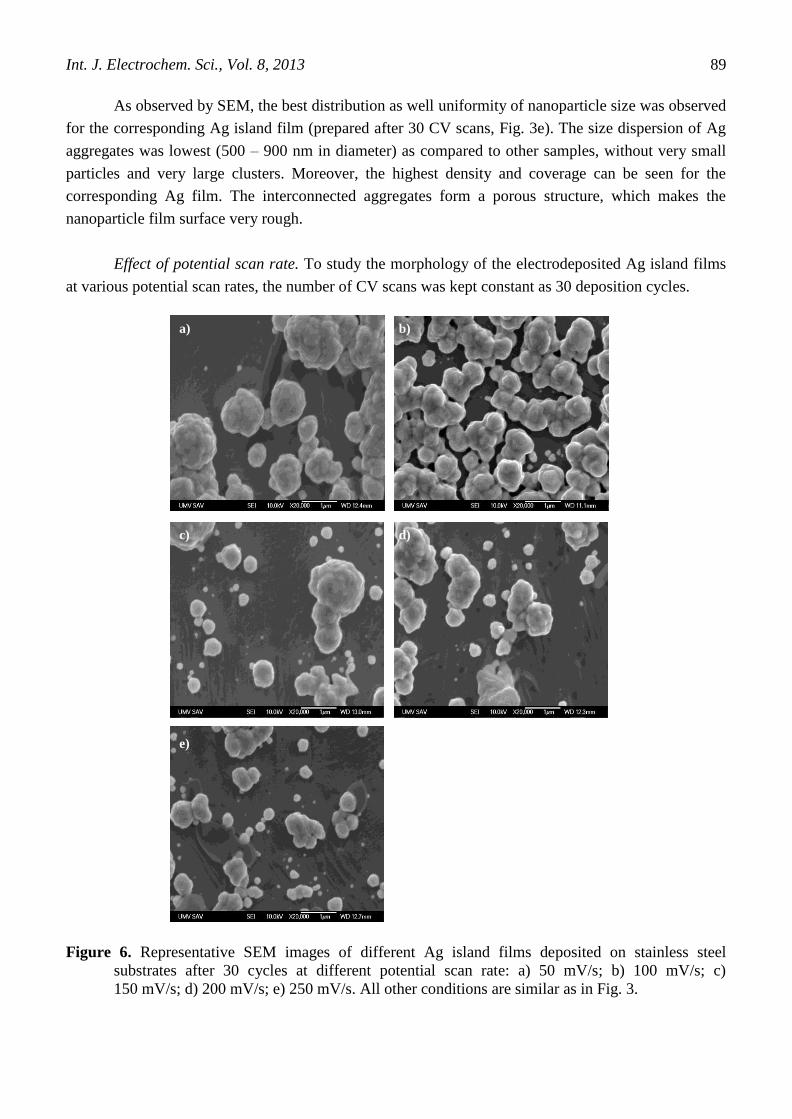
As observed by SEM, the best distribution as well uniformity of nanoparticle size was observed
for the corresponding Ag island film (prepared after 30 CV scans, Fig. 3e). The size dispersion of Ag
aggregates was lowest (500 – 900 nm in diameter) as compared to other samples, without very small
particles and very large clusters. Moreover, the highest density and coverage can be seen for the
corresponding Ag film. The interconnected aggregates form a porous structure, which makes the
nanoparticle film surface very rough.
Effect of potential scan rate. To study the morphology of the electrodeposited Ag island films
at various potential scan rates, the number of CV scans was kept constant as 30 deposition cycles.
Figure 6. Representative SEM images of different Ag island films deposited on stainless steel
substrates after 30 cycles at different potential scan rate: a) 50 mV/s; b) 100 mV/s; c)
150 mV/s; d) 200 mV/s; e) 250 mV/s. All other conditions are similar as in Fig. 3.
a) b)
c) d)
e)
Int. J. Electrochem. Sci., Vol. 8, 2013
90
Figures 6(a) – (e) show representative SEM images of the Ag island films deposited at potential
scan rates of 50, 100, 150, 200 and 250 mV/s, resp. With an increase in potential scan rate, the
spherical nanoparticles and clusters become smaller and less aggregated. Moreover, the lower
coverage of working electrode with Ag nanostructures was observed when the scan rate was increased.
The time of deposition shortens with a rise in scan rate. The formation of Ag nanoparticles and
aggregates involves two competitive processes: growth versus formation of new particles. At lower
potential scan rates, the rate of the growth is slightly higher than that of formation. With increasing
scan rate, the rate of formation increases while the rate of growth decreases. As the potential scan rate
increases, the particle and cluster formation dominates. In consequence, as the scan rate increase from
50 to 250 mV/s, the number of small particles (90 – 270 nm in diameter) increased, the diameter of the
aggregates decreased (from ca. 900 nm to 500 nm in diameter) and the size dispersion becomes
broader.
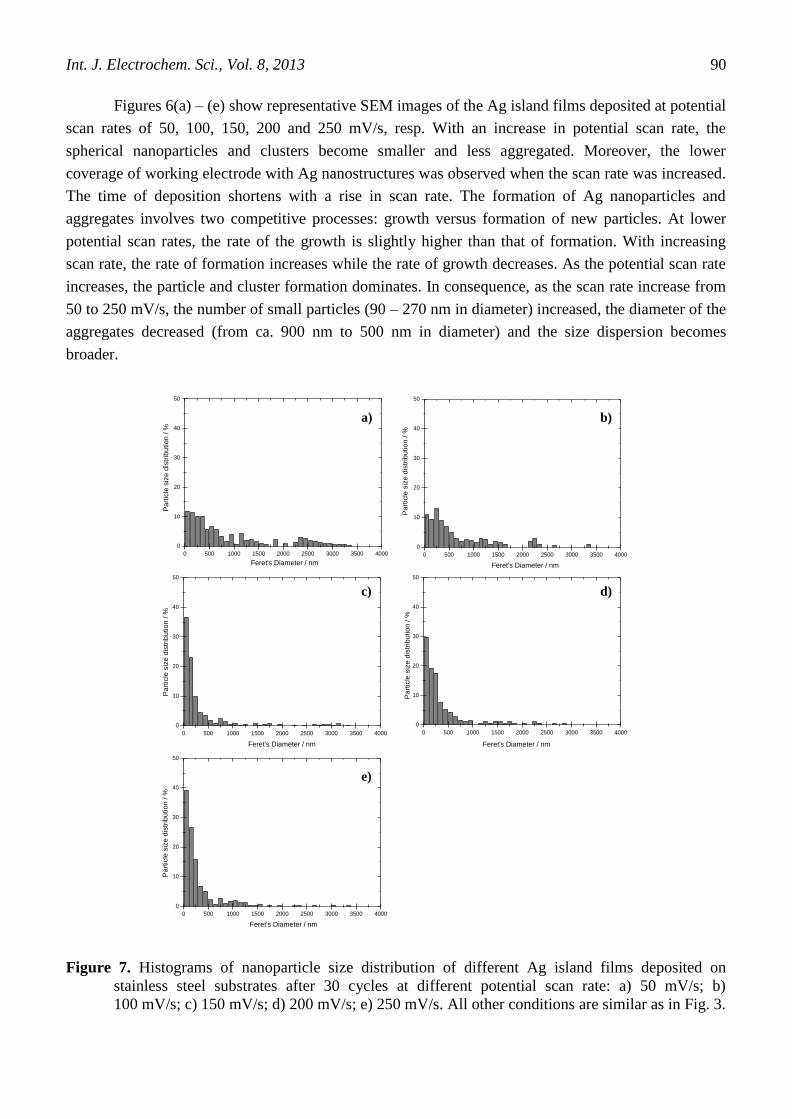
Figure 7. Histograms of nanoparticle size distribution of different Ag island films deposited on
stainless steel substrates after 30 cycles at different potential scan rate: a) 50 mV/s; b)
100 mV/s; c) 150 mV/s; d) 200 mV/s; e) 250 mV/s. All other conditions are similar as in Fig. 3.
0 500 1000 1500 2000 2500 3000 3500 4000
0
10
20
30
40
50
P
art
icle
siz
e d
istr
ibu
tio
n / %
Feret's Diameter / nm
0 500 1000 1500 2000 2500 3000 3500 4000
0
10
20
30
40
50
P
art
icle
siz
e d
istr
ibu
tio
n / %
Feret's Diameter / nm
0 500 1000 1500 2000 2500 3000 3500 4000
0
10
20
30
40
50
P
art
icle
siz
e d
istr
ibu
tio
n / %
Feret's Diameter / nm
0 500 1000 1500 2000 2500 3000 3500 4000
0
10
20
30
40
50
P
art
icle
siz
e d
istr
ibu
tio
n / %
Feret's Diameter / nm
0 500 1000 1500 2000 2500 3000 3500 4000
0
10
20
30
40
50
P
art
icle
siz
e d
istr
ibu
tio
n / %
Feret's Diameter / nm
a)
e)
c) d)
b)
Int. J. Electrochem. Sci., Vol. 8, 2013
91
Figure 7 shows the particle size distribution of Ag nanoparticles produced at different potential
scan rates, corresponding to Fig. 6. It can be seen that the Feret's diameter of the nanoparticles
decreased with increasing scan rate. The number of particles in the range between 2 and 3 m
decreased and number of small particles with the Feret's diameter under 500 nm increased.
500 750 1000 1250 1500 1750 2000
e)
d)
c)
b)
a)
Inte
ns
ity
/ a
.u.
Raman shift / cm-1
Figure 8. Representative SERS spectra of 5×10
−4 mol/l R6G adsorbed on different Ag island films
prepared by multiple scan CV after 30 cycles at different potential scan rate: a) 50 mV/s; b)
100 mV/s; c) 150 mV/s; d) 200 mV/s; e) 250 mV/s.
Fig. 8 shows the influence of the increasing potential scan rate on the corresponding SERS
effect for Ag nanoparticle film electrodeposition from 50 to 250 mV/s. A significant increase in the
Raman intensity was detected for the first increment of potential scan rate from 50 to 100 mV/s.
However, a gradual decrease in the intensity of the signal was observed with a further increase of
potential scan rate. Therefore, the maximum SERS activity was observed on the Ag island nanoparticle
film deposited at 100 mV/s.
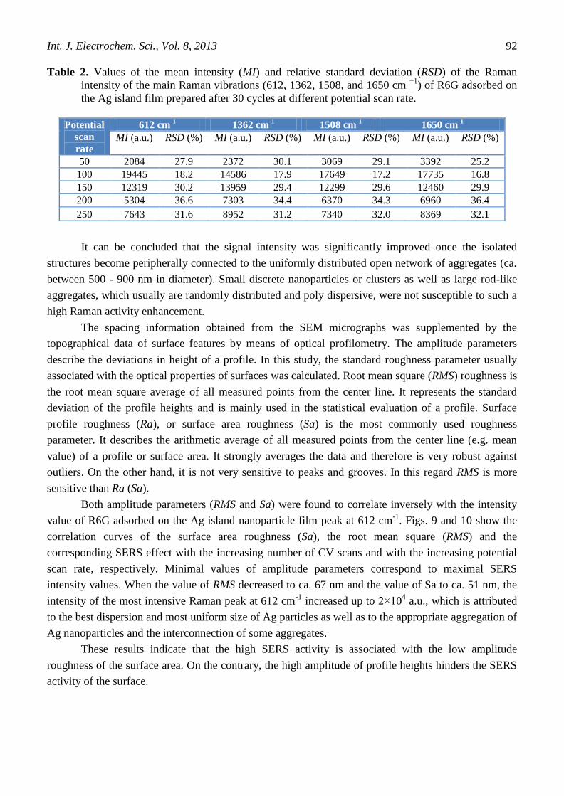
The mean intensity and standard deviation of the main Raman vibrations (612, 1362, 1508, and
1650 cm−1
) of R6G adsorbed on Ag films deposited at different potential scan rates are summarised in
Table 2. The best reproducibility and uniformity of the SERS intensity was obtained for the Ag film
deposited at 100 mV/s. Better surface uniformity clearly generated a more reproducible SERS signal.
Nevertheless, all prepared Ag nanoparticle film provided acceptable reproducibility (better than 40%).
From the SEM images of the Ag nanoparticle films prepared at elevated potential scan rates
(Fig. 6), it can be seen clearly that the highest density of Ag island films on the working electrode
surface, best distribution and low size dispersion of Ag particles was observed for Ag film deposited at
100 mV/s. The uniform aggregates merge together to form an interpenetrating network. It indicates
that the observed highest activity of the mentioned substrate can be related to the resulting overall
porous-like structure.
Int. J. Electrochem. Sci., Vol. 8, 2013
92
Table 2. Values of the mean intensity (MI) and relative standard deviation (RSD) of the Raman
intensity of the main Raman vibrations (612, 1362, 1508, and 1650 cm −1
) of R6G adsorbed on
the Ag island film prepared after 30 cycles at different potential scan rate.
Potential
scan
rate
612 cm-1
1362 cm-1
1508 cm-1
1650 cm-1
MI (a.u.) RSD (%) MI (a.u.) RSD (%) MI (a.u.) RSD (%) MI (a.u.) RSD (%)
50 2084 27.9 2372 30.1 3069 29.1 3392 25.2
100 19445 18.2 14586 17.9 17649 17.2 17735 16.8
150 12319 30.2 13959 29.4 12299 29.6 12460 29.9
200 5304 36.6 7303 34.4 6370 34.3 6960 36.4
250 7643 31.6 8952 31.2 7340 32.0 8369 32.1
It can be concluded that the signal intensity was significantly improved once the isolated
structures become peripherally connected to the uniformly distributed open network of aggregates (ca.
between 500 - 900 nm in diameter). Small discrete nanoparticles or clusters as well as large rod-like
aggregates, which usually are randomly distributed and poly dispersive, were not susceptible to such a
high Raman activity enhancement.
The spacing information obtained from the SEM micrographs was supplemented by the
topographical data of surface features by means of optical profilometry. The amplitude parameters
describe the deviations in height of a profile. In this study, the standard roughness parameter usually
associated with the optical properties of surfaces was calculated. Root mean square (RMS) roughness is
the root mean square average of all measured points from the center line. It represents the standard
deviation of the profile heights and is mainly used in the statistical evaluation of a profile. Surface
profile roughness (Ra), or surface area roughness (Sa) is the most commonly used roughness
parameter. It describes the arithmetic average of all measured points from the center line (e.g. mean
value) of a profile or surface area. It strongly averages the data and therefore is very robust against
outliers. On the other hand, it is not very sensitive to peaks and grooves. In this regard RMS is more
sensitive than Ra (Sa).
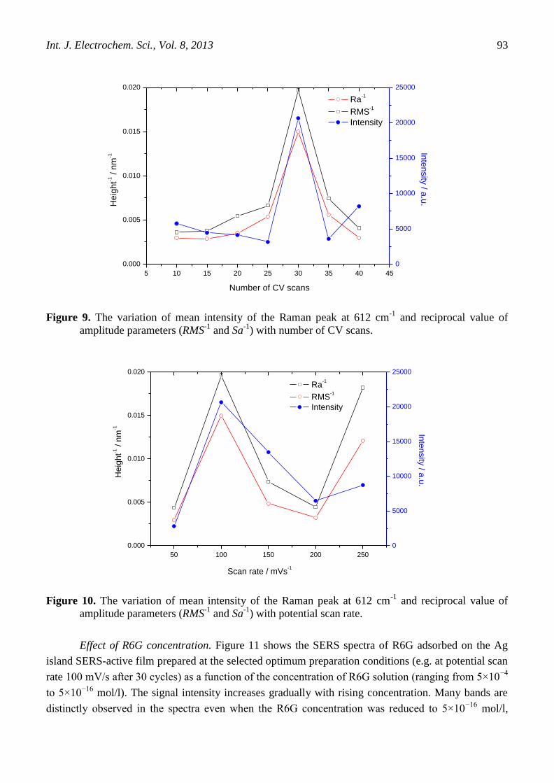
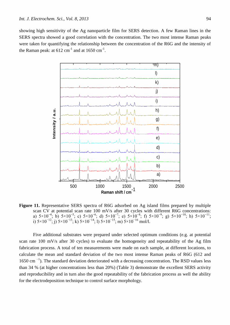
Both amplitude parameters (RMS and Sa) were found to correlate inversely with the intensity
value of R6G adsorbed on the Ag island nanoparticle film peak at 612 cm-1
. Figs. 9 and 10 show the
correlation curves of the surface area roughness (Sa), the root mean square (RMS) and the
corresponding SERS effect with the increasing number of CV scans and with the increasing potential
scan rate, respectively. Minimal values of amplitude parameters correspond to maximal SERS
intensity values. When the value of RMS decreased to ca. 67 nm and the value of Sa to ca. 51 nm, the
intensity of the most intensive Raman peak at 612 cm-1
increased up to 2×10⁴ a.u., which is attributed
to the best dispersion and most uniform size of Ag particles as well as to the appropriate aggregation of
Ag nanoparticles and the interconnection of some aggregates.
These results indicate that the high SERS activity is associated with the low amplitude
roughness of the surface area. On the contrary, the high amplitude of profile heights hinders the SERS
activity of the surface.
Int. J. Electrochem. Sci., Vol. 8, 2013
93
5 10 15 20 25 30 35 40 45
0.000
0.005
0.010
0.015
0.020
He
igh
t-1 / n
m-1
Number of CV scans
Ra-1
RMS-1
Intensity
0
5000
10000
15000
20000
25000
Inte
nsity
/ a.u
.
Figure 9. The variation of mean intensity of the Raman peak at 612 cm
-1 and reciprocal value of
amplitude parameters (RMS-1
and Sa-1
) with number of CV scans.
50 100 150 200 250
0.000
0.005
0.010
0.015
0.020
Ra-1
RMS-1
Intensity
He
igh
t-1 / n
m-1
Scan rate / mVs-1
0
5000
10000
15000
20000
25000
Inte
nsity
/ a.u
.
Figure 10. The variation of mean intensity of the Raman peak at 612 cm
-1 and reciprocal value of
amplitude parameters (RMS-1
and Sa-1
) with potential scan rate.
Effect of R6G concentration. Figure 11 shows the SERS spectra of R6G adsorbed on the Ag
island SERS-active film prepared at the selected optimum preparation conditions (e.g. at potential scan
rate 100 mV/s after 30 cycles) as a function of the concentration of R6G solution (ranging from 5×10⁻⁴
to 5×10⁻¹⁶
mol/l). The signal intensity increases gradually with rising concentration. Many bands are
distinctly observed in the spectra even when the R6G concentration was reduced to 5×10⁻¹⁶
mol/l,
Int. J. Electrochem. Sci., Vol. 8, 2013
94
showing high sensitivity of the Ag nanoparticle film for SERS detection. A few Raman lines in the
SERS spectra showed a good correlation with the concentration. The two most intense Raman peaks
were taken for quantifying the relationship between the concentration of the R6G and the intensity of
the Raman peak: at 612 cm-1
and at 1650 cm-1
.
Figure 11. Representative SERS spectra of R6G adsorbed on Ag island films prepared by multiple
scan CV at potential scan rate 100 mV/s after 30 cycles with different R6G concentrations:
a) 5×10⁻⁴
; b) 5×10⁻⁵
; c) 5×10⁻⁶
; d) 5×10⁻⁷
; e) 5×10⁻⁸
; f) 5×10⁻⁹
; g) 5×10⁻¹⁰
; h) 5×10⁻¹¹
;
i) 5×10⁻¹²
; j) 5×10⁻¹³
; k) 5×10⁻¹⁴
; l) 5×10⁻¹⁵
; m) 5×10⁻¹⁶
mol/l.
Five additional substrates were prepared under selected optimum conditions (e.g. at potential
scan rate 100 mV/s after 30 cycles) to evaluate the homogeneity and repeatability of the Ag film
fabrication process. A total of ten measurements were made on each sample, at different locations, to
calculate the mean and standard deviation of the two most intense Raman peaks of R6G (612 and
1650 cm −1
). The standard deviation deteriorated with a decreasing concentration. The RSD values less
than 34 % (at higher concentrations less than 20%) (Table 3) demonstrate the excellent SERS activity
and reproducibility and in turn also the good repeatability of the fabrication process as well the ability
for the electrodeposition technique to control surface morphology.
500 1000 1500 2000 2500
In
ten
sit
y /
a.u
.
Raman shift / cm-1
a)
b)
c)
d)
e)
f)
g)
h)
i)
j)
k)
l)
m)
Int. J. Electrochem. Sci., Vol. 8, 2013
95
Figure 12. The variation of mean intensity of the Raman peak at 612 cm-1
and at 1650 cm-1
with R6G
concentration.
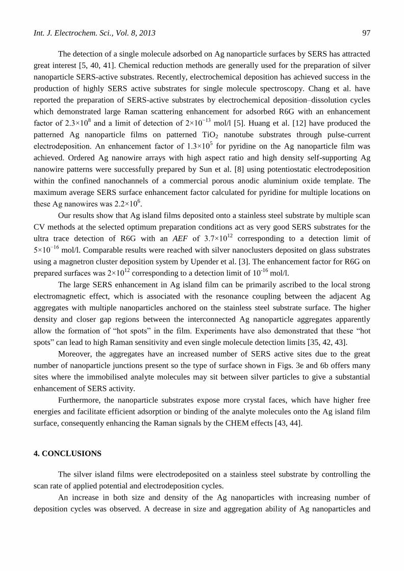
Figure 12 shows the dependence of the mean value of the Raman peaks intensity of R6G
adsorbed on the Ag island SERS-active film prepared at the selected optimum preparation conditions
(e.g. at potential scan rate 100 mV/s after 30 cycles) at 612 cm-1
and 1650 cm-1
as a function of the
concentration of R6G. The solid lines are the linear fits to the data. The intensity of both Raman bands
varies linearly with the logarithmic concentration of R6G over a large concentration range of 12 orders
of magnitude. Several factors may be responsible for this behaviour: lower number of R6G molecule
effectively excitated by the laser beam owing to not only a monolayer coverage of R6G molecules on
the substrate and/or saturation of the surface at high concentration; chemical adsorption of major
portion of R6G molecules on the Ag nanoparticles and so higher contribution from chemical
enhancement, single R6G molecule - Ag nanoparticle interaction, and/or selective occupation of the
“hot spots” until lower concentrations. The minimum detectable concentration was 5×10⁻¹⁶
mol/l.
Corresponding intensities together with values of the determined analytical enhancement factor (AEF)
5E-16 5E-15 5E-14 5E-13 5E-12 5E-11 5E-10 5E-9 5E-8 5E-7 5E-6 5E-5 5E-4
0
5000
10000
15000
20000
25000
Inte
nsity / a
.u.
Concentration of R6G / mol/l
612 cm-1
R2 = 0.9922
5E-16 5E-15 5E-14 5E-13 5E-12 5E-11 5E-10 5E-9 5E-8 5E-7 5E-6 5E-5 5E-4
0
5000
10000
15000
20000
25000
Inte
nsity / a
.u.
Concentration of R6G / mol/l
1650 cm-1
R2 = 0.9934

Int. J. Electrochem. Sci., Vol. 8, 2013
96
are summarized in Table 3. The larger standard deviations at lower concentrations could be attributed
to the absence of chemical enhancement from some molecules as the spectra depend on the size and
shape of the metal nanoparticles as well as on the orientation of adsorbed molecule on the metal
nanoparticle or to the variation of R6G molecules number due to possible dilution inaccuracy and
looseness during transfer to the substrate.
To estimate the enhancement ability of the Ag island film, the AEF was calculated. According
to the method developed by Le Ru et al. [39], AEF is defined as follows:
RS
RS
SERS
SERS
I
c
c
IAEF (1)
where ISERS denotes the mean Raman intensity obtained for the Ag island nanoparticle SERS substrate
under a certain concentration of SERSc , and IRS represents the Raman intensity obtained under non-
SERS conditions on the stainless steel surface coated by continual smooth Ag layer with the thickness
~ 400 m at the R6G concentration of RSc = 1×10⁻³
mol/l. It was difficult to obtain an exact value of
IRS from non-Ag coated stainless steel surface due to strong fluorescence response. RS stands for
“reference sample”. In the present study ISERS and IRS were calculated using 612 and 1650 cm-1
as a
reference peaks.
The prepared SERS-active substrate based on the optimum preparation conditions demonstrates
a large AEF of 3.7×10¹²
(resp. 2.5×10¹²
) which significantly reduces the practical limit of detection of
R6G to 5×10⁻¹⁶
mol/l. The number of the R6G molecules in 1 μl of solution at lower R6G
concentration (5×10⁻¹⁶
mol/l) is: 5×10−16
× 10−6
× 6.02×1023
= 301. The number of molecules actually
illuminated by the laser beam should be lower.
Table 3. Values of mean intensity (MI) and relative standard deviation (RSD) of the Raman peak of
R6G adsorbed on the Ag island SERS-active film prepared at the selected optimum preparation
conditions (e.g. at potential scan rate 100 mV/s after 30 cycles) at 612 cm-1
and 1650 cm-1
together with the determined values of AEF as a function of the R6G concentration.
R6G
concentration
(mol/l)
612 cm-1
1650 cm-1
MI (a.u.) RSD (%) AEF MI (a.u.) RSD (%) AEF
5×10⁻⁴
1977 8 13.2 6.6×101 18426 11.4 5.3×10
1
5×10⁻⁵
16981 11.1 5.7×10² 17187 11.1 4.9×10
2
5×10⁻⁶
15482 10.3 5.2×10³ 15369 11.5 4.4×10
3
5×10⁻⁷
14849 10.7 5.0×10⁴ 13126 11.3 3.8×10
4
5×10⁻⁸
13414 13.1 4.5×10⁵ 11691 14.1 3.4×10
5
5×10⁻⁹
11031 16.4 3.7×10⁶ 10398 13.1 3.0×10
6
5×10⁻¹⁰
8883 23.4 3.0×10⁷
8990 21.7 2.6×10⁷
5×10⁻¹¹
8062 17.7 2.7×10⁸ 7661 15.7 2.2×10
8
5×10⁻¹²
6123 23.9 2.1×10⁹ 5389 23.2 1.5×10
9
5×10⁻¹³
4657 22.5 1.6×10¹⁰
3740 22.6 1.1×10¹⁰
5×10⁻¹⁴
3950 24.8 1.3×10¹¹
2402 27.4 6.9×10¹⁰
5×10⁻¹⁵
1848 30.8 6.1×10¹¹
1274 32.1 3.7×10¹¹
5×10⁻¹⁶
1099 32.2 3.7×10¹²
864 33.5 2.5×10¹²
Int. J. Electrochem. Sci., Vol. 8, 2013
97
The detection of a single molecule adsorbed on Ag nanoparticle surfaces by SERS has attracted
great interest [5, 40, 41]. Chemical reduction methods are generally used for the preparation of silver
nanoparticle SERS-active substrates. Recently, electrochemical deposition has achieved success in the
production of highly SERS active substrates for single molecule spectroscopy. Chang et al. have
reported the preparation of SERS-active substrates by electrochemical deposition–dissolution cycles
which demonstrated large Raman scattering enhancement for adsorbed R6G with an enhancement
factor of 2.3×10⁸ and a limit of detection of 2×10
−13 mol/l [5]. Huang et al. [12] have produced the
patterned Ag nanoparticle films on patterned TiO2 nanotube substrates through pulse-current
electrodeposition. An enhancement factor of 1.3×10⁵ for pyridine on the Ag nanoparticle film was
achieved. Ordered Ag nanowire arrays with high aspect ratio and high density self-supporting Ag
nanowire patterns were successfully prepared by Sun et al. [8] using potentiostatic electrodeposition
within the confined nanochannels of a commercial porous anodic aluminium oxide template. The
maximum average SERS surface enhancement factor calculated for pyridine for multiple locations on
these Ag nanowires was 2.2×10⁶.
Our results show that Ag island films deposited onto a stainless steel substrate by multiple scan
CV methods at the selected optimum preparation conditions act as very good SERS substrates for the
ultra trace detection of R6G with an AEF of 3.7×10¹²
corresponding to a detection limit of
5×10⁻¹⁶
mol/l. Comparable results were reached with silver nanoclusters deposited on glass substrates
using a magnetron cluster deposition system by Upender et al. [3]. The enhancement factor for R6G on
prepared surfaces was 2×10¹²
corresponding to a detection limit of 10-16
mol/l.
The large SERS enhancement in Ag island film can be primarily ascribed to the local strong
electromagnetic effect, which is associated with the resonance coupling between the adjacent Ag
aggregates with multiple nanoparticles anchored on the stainless steel substrate surface. The higher
density and closer gap regions between the interconnected Ag nanoparticle aggregates apparently
allow the formation of “hot spots” in the film. Experiments have also demonstrated that these “hot
spots” can lead to high Raman sensitivity and even single molecule detection limits [35, 42, 43].
Moreover, the aggregates have an increased number of SERS active sites due to the great
number of nanoparticle junctions present so the type of surface shown in Figs. 3e and 6b offers many
sites where the immobilised analyte molecules may sit between silver particles to give a substantial
enhancement of SERS activity.
Furthermore, the nanoparticle substrates expose more crystal faces, which have higher free
energies and facilitate efficient adsorption or binding of the analyte molecules onto the Ag island film
surface, consequently enhancing the Raman signals by the CHEM effects [43, 44].
4. CONCLUSIONS
The silver island films were electrodeposited on a stainless steel substrate by controlling the
scan rate of applied potential and electrodeposition cycles.
An increase in both size and density of the Ag nanoparticles with increasing number of
deposition cycles was observed. A decrease in size and aggregation ability of Ag nanoparticles and
Int. J. Electrochem. Sci., Vol. 8, 2013
98
clusters, resulting in lower coverage of the working electrode, was registered with an increase in
potential scan rate.
The strongest SERS effect was associated with the Ag nanoparticle films characterized by the
best distribution, highest density and low size dispersion of nanoparticles. The significant enhancement
of SERS activity was detected once the isolated structures become interconnected to form the
uniformly distributed network providing many sites for analyte molecules.
The amplitude parameters of surface features were found to correlate inversely with the
intensity value of R6G adsorbed on the Ag island nanoparticle film
The results suggest that the SERS enhancements arise from both the EM and CHEM effects.
The large enhancement is mainly attributed to junctions of particle aggregates and is associated partly
also with the unique surface properties, favouring interactions with analyte molecules.
The less than 20% RSD of the Raman intensity of the carbon skeleton stretching modes for the
Ag nanoparticle film prepared at the selected optimum preparation conditions clearly demonstrated the
high uniformity and reproducibility of the substrate as well good repeatability of the electrochemical
fabrication process.
Ag island films deposited onto stainless steel substrate by multiple scan CV methods at the
selected optimum preparation conditions (e.g. at potential scan rate 100 mV/s after 30 cycles) act as
very good SERS substrates for the ultra trace detection of R6G with an AEF of 3.7×10¹²
,
corresponding to a detection limit of 5×10⁻¹⁶
mol/l.
The presented Ag island films could improve the detection limit of R6G by four orders of
magnitude as compared to previous reports dealing with the electrochemical fabrication of SERS
active substrates. As the electrochemical deposition is very simple and inexpensive, it may be used in
large-scale preparation of substrates that could be widely applied in Raman analysis.
ACKNOWLEDGEMENTS
Financial support from Grant VEGA No. 1/0211/12 of the Slovak Scientific Grant Agency is highly
acknowledged.
References
1. M. E. Abdelsalam, P. N. Bartlett, J. J. Baumberg, S. Cintra, T. A. Kelf and A.E. Russell,
Electrochem. Comm., 7 (2005) 740.
2. I. M. I. Ismail, J. Saudi Chem. Soc., 14 (2010) 351.
3. G. Upender, R. Satyavathi, B. Raju, K. Shadak Alee, D. Narayana Rao and C. Bansal, Chem.
Phys. Lett,. 511 (2011) 309.
4. K. H. Yang, Y. Ch. Liu and Ch. Ch. Yu, Electrochim. Acta, 54 (2009) 4202.
5. Ch. Ch. Chang, K. H. Yang, Y. Ch. Liu and Ch. Ch. Yu, Anal. Chimica Acta, 709 (2012) 91.
6. Ch. Zhu, G. Meng, Q. Huang and Z. Huang, J. Hazard. Mater., 211–212 (2012) 389.
7. M. Fan, G. F. S. Andrade and A. G. Brolo, Anal. Chim. Acta, 693 (2011) 7.
8. B. Sun, X. Jiang, S. Dai and Z. Du, Mater. Lett., 63 (2009) 2570.
9. C. Jing and Y. Fang, J. Colloid Interface Sci., 314 (2007) 46.
10. R. Sanci and M. Volkan, Sensors Actuator B Chem., 139 (2009) 150.
Int. J. Electrochem. Sci., Vol. 8, 2013
99
11. Z. Lu, Y. Gu, J. Yang, Z. Li, W. Ruan, W. Xu, Ch. Zhao and B. Zhao, Vib. Spectrosc., 47 (2008)
99.
12. Y. Huang, L. Sun, K. Xie, Y. Lai, B. Liu, B. Rena and Ch. Lin, J. Raman Spectrosc., 42 (2011)
986.
13. E. Hao and G. C. Schatz, J. Chem. Phys., 120 (2004) 357.
14. C .J. Orendorff, L. Gearheart, N. R. Jana and C. J. Murphy, Phys. Chem. Chem. Phys., 8 (2006)
165.
15. M. Fleischmann, P. J. Hendra and A. J. McQuillan, Chem. Phys. Lett., 26 (1974) 163.
16. R. Foucault, R. L. Birke and J. R. Lombardi, Langmuir, 19 (2003) 8818.
17. I. Baltog, N. Primeau, R. Reinish and J. L. Coutaz, Appl. Phys. Lett., 66 (1995) 1187.
18. P. C. Lee and D. Meisel, J. Phys. Chem., 86 (1982) 3391.
19. R. G. Freeman, K. C. Grabar, K. J. Allison, R. M. Bright, J. A. Davis, A. P. Guthrie, M. B.
Hommer, M. A. Jackson, P. C. Smith, D. G. Walter and M. J. Natan, Science, 267 (1995) 1629.
20. Z. Q. Tian, B. Ren and D. Y. Wu, J. Phys. Chem. B, 106 (2002) 9463.
21. B. H. Loo, J. Electroanal. Chem., 136 (1982) 209.
22. H. Yamada and Y. Yamamoto, Surf. Sci., 134 (1983) 71.
23. R. De Mondt, K. Baert, I. Geuens, L. Van Vaeck and A. Hubin, Langmuir, 22 (2006) 11360.
24. J. D. Driskell, S. Shanmukh, Y. Liu, S. B. Chaney, X. J. Tang, Y. P. Zhao and R. A. Dluhy, J.
Phys. Chem. C, 112 (2008) 895.
25. L. Wang, Y. Sun, G. Che and Z. Li, Appl. Surf. Sci., 257 (2011) 7150.
26. C. Domingo, V. Resta, S. Sanchez-Cortes, J. V. Garcia-Ramos and J. Gonzalo, J. Phys. Chem. C,
111 (2007) 8149.
27. K. H. Yang, Y. C. Liu and C. C. Yu, Langmuir, 26 (2010) 11512.
28. M. Pagannone, L. G. Quagliano, L. Mattioli and G. Mattei, J. Raman Spectrosc., 22 (1991) 825.
29. L. P. Bicelli, B. Bozzini, C. Mele and L. D'Urzo, Int. J. Electrochem. Sci., 3 (2008) 356.
30. W. Wei, X. Mao, L. A. Ortiz and D. R. Sadoway, J. Mater. Chem., 21 (2011) 432.
31. D. K. Sharma, A. Ott, A. P. O’Mullane and S. K. Bhargava, Colloid Surface Physicochem. Eng.
Aspect, 386 (2011) 98.
32. Y. Chen, B. Dong and W. Zhou, Appl. Surf. Sci., 257 (2010) 1021.
33. A. T. Dimitrov, S. Hadzijordanov, K. I. Popov, M. G. Pavlovic and V. Radmilovic, J. Appl.
Electrochem.. 28 (1998) 791.
34. A. Gutes, C. Carraro and R. Maboudian, ACS Appl. Mater. Interface, 1 (2009) 2551.
35. Y. Lu, G. L. Liu and L. P. Lee, Nano Lett., 5 (2005) 5.
36. Z. Sun, Y. Li, Y. Wang, X. Chen, J. Zhang, K. Zhang, Z. Wang, C. Bao, J. Zeng, B. Zhao and B.
Yang, Langmuir, 23 (2007) 10725.
37. L. Jensen and G. C. Schatz, J. Phys. Chem. A, 110 (2006) 5973.
38. M. J. Natan, Faraday Discuss., 132 (2006) 321.
39. E. C. Le Ru, E. Blackie, M. Meyer and P. G. Etchegoin, J. Phys. Chem. C, 111 (2007) 13794.
40. W. E. Doering and S. Nie, J. Phys. Chem. B, 106 (2002) 311.
41. P. Etchegoin, R. C. Maher, L. F. Cohen, H. Hartigan, R. J. C. Brown, M. J. T. Milton and J. C.
Gallop, Chem. Phys. Lett., 375 (2003) 84.
42. C. Cheng, B. Yan, S.M. Wong, X. Li, W. Zhou, T. Yu, Z. Shen, H. Yu and H. J. Fan, Appl. Mater.
Interfaces, 2 (2010) 1824.
43. W. C. Zhang, X. L. Wu, C. X. Kan, F. M. Pan, H. T. Chen, J. Zhu and P. K. Chu, Appl. Phys. A,
100 (2010) 83.
44. A. M. Schwartzberg, C. D. Grant, A. Wolcott, C. E. Talley, T. R. Huser, R. Bogomolni and J. Z.
Zhang, J. Phys. Chem. B, 108 (2004) 19191.
© 2013 by ESG (www.electrochemsci.org)