electrode characteristics of individual, mno2 coated
TRANSCRIPT

Electrode Characteristics of Individual, MnO2 Coated Carbon Nanotubes
Brad L. Corso, Israel Perez, and Philip G. Collins
Department of Physics and Astronomy, University of California Irvine, Irvine CA 92697
We investigate interfacial charge transfer between a manganese oxide (MnO2) pseudocapacitor material and graphitic carbon supports in the limit where the graphitic carbon is defect free. We achieve this limit experimentally by fabricating model electrodes comprising MnO2 deposited on single, pristine, isolated single-walled carbon nanotubes. Li ion cyclic voltammetry of the composites gives a specific capacitance in accord with MnO2 storage capacities, but with kinetics limited by the poor electron transfer properties of defect free carbon. By fitting the data to an equivalent circuit model, we determine the charge transfer resistivity of MnO2-carbon interfaces to be 9 x 10⁷ Ω-cm when defects are absent, a limiting value for high power cathodes.
1. Introduction Graphitic carbons and manganese oxide (MnO2) are both promising materials for heterogeneous, nanostructured pseudocapacitors because of the synergies between graphite’s high conductance and stability and MnO2’s low cost and high theoretical specific capacitance (1, 2). However, existing carbon-MnO2 composites do not achieve the full potential of both materials. This paper investigates some of the interfacial properties that can play limiting roles. Specifically, we consider the fundamental charge transfer resistance across the carbon-MnO2 interface, and the role of carbon defect sites in reducing that resistance.
It is well established that defect sites, especially those which contain oxygen, promote more efficient electron transfer by carbon electrodes (3-6). However a quantitative measure of the defect-free case has been historically elusive. High quality carbon systems all contain defects, whether at basal plane edges, grain boundaries, or points. As a result, all graphitic electrodes are ensemble mixtures of electrochemically active defects among basal plane carbon. As described in the recent review article by McCreery (3), precise control over the concentration and chemistry of defects is necessary before the fundamental electron transfer rates of these sites can be established quantitatively.
To address this issue, we investigate electrochemical processes on the sidewall of a single carbon nanotube. Using high quality, single-walled carbon nanotubes (SWNTs) that are grown in place without further processing or manipulation, we interrogate carbon electrodes in the limit of defect-free carbon. Our SWNTs are electrically connected in a field effect transistor (FET) geometry, so that they can be used as both electrochemical working electrodes and as FET devices. SWNTs have an electrical conductivity that is particularly sensitive to the presence of defects (7), and this property can be exploited to characterize defects with single site sensitivity (8, 9).

2. Materials and Methods 2a. Carbon Nanotube Synthesis and Device Fabrication
SWNTs were synthesized using a monodisperse nanoparticle of Fe30Mo84 as the
catalytic seed for a conventional chemical vapor deposition (CVD) process. The catalyst seeds were the result of oxidizing a giant metallorganic cluster surrounded by ligand-terminated, icosahedral FeMo cages. Our synthesis of the metallorganic cluster reproduced previous reports (10, 11). The clusters were diluted in ethanol (30 mg/L), and then 0.5 mL of solution was spincast onto 4” p++ Si/SiO2 wafers to give a dilute coating of catalyst particles. The resulting areal density of particles, approximately 0.1 μm-2, is satisfactory for growing dilute and isolated SWNTs.
CVD growth of SWNTs was accomplished in a custom-built, 6” quartz tube furnace operating at 940 °C. A carrier gas of Ar (3000 sccm) was used in combination with feedstocks of H2 (520 sccm) and CH4 (1000 sccm). Similar conditions in a smaller furnace have been reported to grow SWNTs with long lengths and excellent electrical characteristics (11, 12). The resulting SWNTs were characterized by a combination of scanning electron microscopy (SEM, Philips XL-30 at 1 kV and 20 kV) and by noncontact atomic force microscopy (AFM, Pacific Nanotechnology Nano-R). We observed a SWNT diameter range of 1.1 – 1.6 nm.
After CVD, wafers were processed with optical lithography to define Ti electrodes on top of the randomly grown SWNTs. We used an undercut bilayer resist (S1808 on top of LOR-A1, MicroChem) to improve liftoff and give clean interfaces. The FET source-drain separation was designed to be 2 μm. The p++ substrate, separated from the SWNTs by a 500 nm thermal oxide, provided a backgate electrode for each device on the wafer. Wafer-scale electrical characterization identified about 30% of the SWNTs devices as metallic and 70% as semiconducting, consistent with the 1:2 ratio predicted theoretically.
After initial characterization, each device underwent a step of electron beam lithography. Devices were coated in electron beam resist (A3 PMMA, MicroChem) and patterned to expose an active SWNT channel 0.5 – 1.0 μm in length. This patterning ensured that the majority of the surface, including source and drain electrodes, remained protected from the test solution. Devices were re-imaged by AFM after electron beam lithography to confirm that a SWNT was, in fact, exposed and that it remained free of particulates.
2b. Electrochemical Techniques
Electrochemical depositions and characterizations were accomplished using small
droplets of electrolyte covering the exposed SWNT regions. A schematic of the device setup is shown in Figure 1. Using an xyz manipulator, PTFE microtubing (0.8 mm ID) containing the desired electrolyte was positioned over the desired region and lowered into contact with the surface. The liquid potential was controlled using a Pt pseudo-reference electrode located immediately next to the chip surface. Simultaneously, recordings were made of a Ag/AgCl reference electrode at the distant, reservoir end of the tubing.
Half-cell electrochemical measurements were made using a custom-built, multipotential bipotentiostat controlled using LabVIEW software. The SWNT source, drain, and gate electrodes, as well as an additional Pt counter electrode, were all independently controlled with respect to the Pt pseudo-reference. In this scheme, the working electrode was the exposed SWNT, and electrochemical currents from the

counter electrode to the SWNT were recorded with the aid of a transimpedance current preamplifier (Keithley 428). By using a small (e.g. 50 mV) source-drain bias, the conductance along the SWNT could be independently monitored during electrochemical modifications (9).
Figure 1. Schematic of the setup for electrochemistry on a single SWNT. Counter and reference electrodes are integral to the microtubing, which is positioned over the SWNT device using an xyz manipulator under a microscope.
Delta-phase MnO2 films 250 – 450 nm thick were deposited on individual, exposed
SWNTs using a technique described previously (13), and illustrated below in Figure 2. Briefly, a manganese(II) acetate tetrahydrate (MnAc, 10 mM aqueous) electrolyte is initially deposited all along the SWNT wall, using a brief 10 ms pulse of 1.0V (vs. Pt). The short duration of this pulse nucleates a uniform coating of MnO2 seed particles on the SWNT while also minimizing the creation of SWNT sidewall defects, as monitored by the SWNT conductance. After nucleation, conformal MnO2 coatings may be deposited with excellent uniformity at much lower growth rates of ~1 nm/s. Typical depositions are accomplished with an additional lithium perchlorate (LiClO4, 250 mM) supporting electrolyte, in order to incorporate Li ions and lattice vacancies into the MnO2 lattice (14). Deposition potentials of 0.7 V produce MnO2 films having specific capacitances of 500 F/g and Li ion diffusion coefficients of 6 x 10⁻⁹ cm2/s. With high capacitance and high diffusivity, these films are ideal for probing charge transfer across the carbon supporting electrode.
Figure 2. Scanning electron microscope image of an example device.

After preparation of each device, cyclic voltammograms (CVs) were acquired in aqueous LiClO4. Typically, 60 scans were performed over a range of scan rates that were decreased from 150 to 15 mV/s, and then increased back up to 150 mV/s in order to test reproducibility. To minimize MnO2 dissolution, the range of working potentials was kept relatively low, at 0.2 to 0.8 V (vs. Ag/AgCl). Before and after CVs, each device was imaged by AFM to rule out the irreversible loss of material and to estimate the active volume of MnO2 in each device.
3. Results Figure 3a shows one scan rate series for MnO2-coated SWNT. This sample has an
unusually high active area with 4 μm of exposed SWNT, all uniformly coated by 250 nm of MnO2. Thus, it provides a clear upper maximum to the types of currents observed in the CVs. At 150 mV/s, approximately 10 pA of pseudocapacitive charging and discharging current is observed. At 15 mV/s, the current shrinks to less than a few pA. The apparatus and intrinsic SWNT capacitance provide a measurement baseline that is less than 0.1 pA, as shown in Fig. 3b.
Figure 3. (a) Typical scan rate series of cyclic voltammograms from a MnO2-coated SWNT. (b) Baseline noise and capacitance for an uncoated SWNT measures < 50 fA.
4. Equivalent Circuit and Analysis
4a. Equivalent Circuit Model Specific aspects of interest in a pseudocapacitor include the diffusion resistance,
charge transfer resistance, double layer capacitance, and pseudocapacitance. Typically, these are investigated using electrochemical impedance spectroscopy (EIS). In EIS, the working electrode is driven with a sinusoidal potential (or current) and the response is monitored over a wide range of frequencies. This frequency-dependent technique is ill-suited to nanoscale interfaces having very small currents, because accurate measurements require longer averaging times.
Instead, we attempt to determine the pseudocapacitive properties, and in particular the charge transfer resistance, using an equivalent circuit model to which the CV data may be fit. The model used is shown below in Figure 4.
b) a)

Figure 4. (a) Most general equivalent circuit for a SWNT-MnO2 half-cell electrode, depicted on top of a schematic cross-section of the actual device to visually represent the physical origin of different components. The grey rectangle represents the SWNT working electrode, the pink semi-oval on top of it represents the MnO2, and the largest semi-oval represents the LiClO4 electrolyte. (b) A reduced circuit containing the dominant elements.
The most general equivalent circuit, shown in Fig. 4a, contains all of the possible
interfacial resistances and capacitances of the SWNT-MnO2 system. The electrolyte resistance Rliq, and the SWNT resistance RC are both included for completeness. A more critical impedance for the system is the charge transfer resistance RCT. Our analysis aims to determine the value of RCT for the case of defect-free SWNTs.
Of the capacitive terms, both capacitive and pseudocapacitive components are shown. A non-Faradaic double-layer capacitance CDL exists between the entire working electrode and the electrolyte. While the porous nature of the MnO2 allows for a large surface area-to-volume ratio, the measurements indicate that CDL contributes less than 10% of the total system capacitance. More important is a pair of pseudocapacitances, denoted as Cφ,S and Cφ,B for the surface and bulk terms, respectively. Together, these represent the Li ion storage capacity of the MnO2. The two are distinguished by their kinetics: the surface term Cφ,S draws electrons through the bulk MnO2 electrical resistance, RMnO2, whereas the bulk term Cφ,B charges and discharges through both RMnO2 and RW, the Warburg resistance associated with Li ion diffusion resistance (15).
RW is a non-ohmic function of both voltage and scan-rate and it can be the most limiting resistance in thick film devices. CV measurements of thick MnO2 coatings (500 – 1200 nm) are decidedly multicomponent as RW grows larger. By keeping the coating below 350 nm, on the other hand, the contribution of RW has been minimized. At our typical thicknesses, the measured diffusion coefficients of >10-9 cm2/s indicate that Li ion mobility is not limiting.
These considerations lead us to simplify the equivalent circuit to have only three components, as shown in Fig. 4b. The bulk and surface pseudocapacitances combine into a single capacitance Cφ, because they are indistinguishable when the primary resistance
a) b)
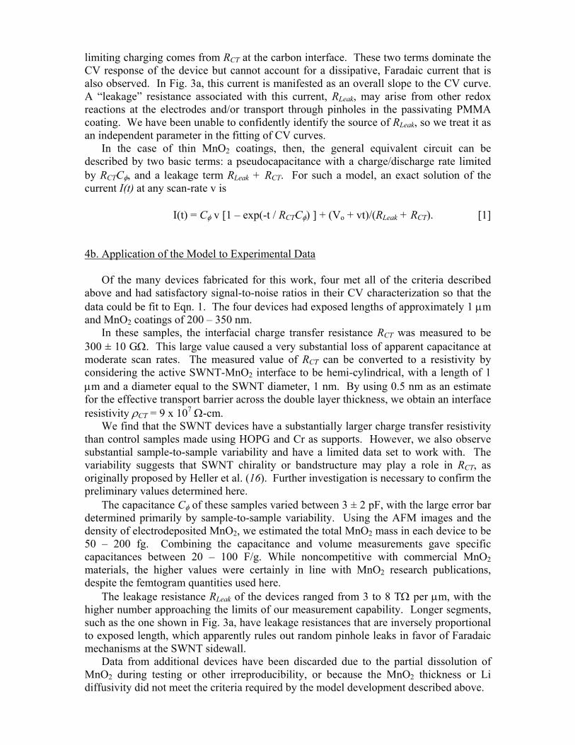
limiting charging comes from RCT at the carbon interface. These two terms dominate the CV response of the device but cannot account for a dissipative, Faradaic current that is also observed. In Fig. 3a, this current is manifested as an overall slope to the CV curve. A “leakage” resistance associated with this current, RLeak, may arise from other redox reactions at the electrodes and/or transport through pinholes in the passivating PMMA coating. We have been unable to confidently identify the source of RLeak, so we treat it as an independent parameter in the fitting of CV curves.
In the case of thin MnO2 coatings, then, the general equivalent circuit can be described by two basic terms: a pseudocapacitance with a charge/discharge rate limited by RCTCφ, and a leakage term RLeak + RCT. For such a model, an exact solution of the current I(t) at any scan-rate v is
I(t) = Cφ v [1 – exp(-t / RCTCφ) ] + (Vo + vt)/(RLeak + RCT). [1]
4b. Application of the Model to Experimental Data Of the many devices fabricated for this work, four met all of the criteria described
above and had satisfactory signal-to-noise ratios in their CV characterization so that the data could be fit to Eqn. 1. The four devices had exposed lengths of approximately 1 μm and MnO2 coatings of 200 – 350 nm.
In these samples, the interfacial charge transfer resistance RCT was measured to be 300 ± 10 GΩ. This large value caused a very substantial loss of apparent capacitance at moderate scan rates. The measured value of RCT can be converted to a resistivity by considering the active SWNT-MnO2 interface to be hemi-cylindrical, with a length of 1 μm and a diameter equal to the SWNT diameter, 1 nm. By using 0.5 nm as an estimate for the effective transport barrier across the double layer thickness, we obtain an interface resistivity ρCT = 9 x 10⁷ Ω-cm.
We find that the SWNT devices have a substantially larger charge transfer resistivity than control samples made using HOPG and Cr as supports. However, we also observe substantial sample-to-sample variability and have a limited data set to work with. The variability suggests that SWNT chirality or bandstructure may play a role in RCT, as originally proposed by Heller et al. (16). Further investigation is necessary to confirm the preliminary values determined here.
The capacitance Cφ of these samples varied between 3 ± 2 pF, with the large error bar determined primarily by sample-to-sample variability. Using the AFM images and the density of electrodeposited MnO2, we estimated the total MnO2 mass in each device to be 50 – 200 fg. Combining the capacitance and volume measurements gave specific capacitances between 20 – 100 F/g. While noncompetitive with commercial MnO2 materials, the higher values were certainly in line with MnO2 research publications, despite the femtogram quantities used here.
The leakage resistance RLeak of the devices ranged from 3 to 8 TΩ per μm, with the higher number approaching the limits of our measurement capability. Longer segments, such as the one shown in Fig. 3a, have leakage resistances that are inversely proportional to exposed length, which apparently rules out random pinhole leaks in favor of Faradaic mechanisms at the SWNT sidewall.
Data from additional devices have been discarded due to the partial dissolution of MnO2 during testing or other irreproducibility, or because the MnO2 thickness or Li diffusivity did not meet the criteria required by the model development described above.

Conclusions It has been shown that MnO2 can be uniformly and controllably deposited onto short
SWNT segments to create pseudocapacitor devices many orders of magnitude smaller than typical pseudocapacitor devices. Optimum MnO2 coatings with thicknesses of 150 – 350 nm give reasonable specific capacitances and fast diffusion constants: when normalized by mass, these small devices have similar performance to larger devices. The primary benefit of working at such a small scale is precise control over the interface between the heterogeneous materials. Using SWNT segments only 1 – 2 μm in length guarantees defect-free carbon interfaces that are difficult to achieve by other means.
Acknowledgments
This material is based upon work supported as part of the Nanostructures for Electrical Energy Storage, an Energy Frontier Research Center funded by the U.S. Department of Energy, Office of Science, Office of Basic Energy Sciences under Award Number DESC0001160.
References
1. C. Liu, F. Li, L. P. Ma, H. M. Cheng, Advanced Materials 22, E28 (2010). 2. C. Jinhua et al., Diamond and Related Materials 15, 1478 (2006). 3. R. L. McCreery, Chemical Reviews 108, 2646 (2008). 4. T. J. Davies, R. R. Moore, C. E. Banks, R. G. Compton, Journal of
Electroanalytical Chemistry 574, 123 (2004). 5. K. R. Kneten, R. L. McCreery, Analytical Chemistry 64, 2518 (1992). 6. L. J. Fu et al., Solid State Sci. 8, 113 (2006). 7. P. G. Collins, in Oxford Handbook of Nanoscience and Technology: Frontiers
and Advances A. V. Narlikar, Y. Y. Fu, Eds. (Oxford Univ. Press, Oxford, 2010). 8. Y. Fan, B. R. Goldsmith, P. G. Collins, Nat. Mat. 4, 906 (2005). 9. B. R. Goldsmith et al., Science 315, 77 (2007). 10. A. Müller et al., Angew. Chem.-Int. Edit. 39, 3414 (2000). 11. L. An, J. M. Owens, L. E. McNeil, J. Liu, J. Am. Chem. Soc. 124, 13688 (2002). 12. S. M. Huang, B. Maynor, X. Y. Cai, J. Liu, Adv. Mater. 15, 1651 (2003). 13. I. Perez, B. L. Corso, V. R. Khalap, P. G. Collins, Electrochemistry
Communications 13, 590 (2011). 14.M. Nakayama, T. Kanaya, J. W. Lee, B. N. Popov, Journal of Power Sources 179,
361 (2008). 15. B. A. Boukamp, I. D. Raistrick, R. A. Huggins, Fast Ion Transport in Solids.
Electrodes and Electrolytes, 177 (1979). 16. I. Heller, J. Kong, K. A. Williams, C. Dekker, S. G. Lemay, J. Am. Chem. Soc.
128, 7353 (2006).