electrodeposition of indium sulfide (in2s3) films on molybdenum-coated glass
TRANSCRIPT

Electrodeposition of Indium Sulfide (In2S3) Films on Molybdenum-coated Glass
Maqsood Ali Mughal
2013 Spring Weekly Research MeetingOctober 8th, 2012
Electronics Lab LSW 156Arkansas State University

Factors And Levels
LevelsA, Deposition
Voltage DV (V)
B, Deposition Time DT
(min)
C, Composition of Solution COS
D, Deposition Temperature D
Temp(OC)
1 -0.6 3 0.1M S 150
2 -0.7 60.1 MS, 0.1M Na2S2O3.5H2O
160
3 -0.8 9 0.2M S 170

Experiment No. A B C D Trial 1 Trial 2 Trial 31 1 1 1 1 √ √ √2 1 1 2 2 √ √ √3 1 1 3 3 √ √ √4 1 2 1 2 √ √ √5 1 2 2 3 √ √ √6 1 2 3 1 √ √ √7 1 3 1 3 √ √ √8 1 3 2 1 √ √ √9 1 3 3 2 √ √ √10 2 1 1 2 √ √ √11 2 1 2 3 √ √ √12 2 1 3 1 √ √ √13 2 2 1 3 √ √ √14 2 2 2 1 √ √ √15 2 2 3 2 √ √ √16 2 3 1 1 √ √ √17 2 3 2 2 √ √ √18 2 3 3 3 √ √ √19 3 1 1 3 √ √ √20 3 1 2 1 √ √ √21 3 1 3 2 √ √ √22 3 2 1 1 √ √ √23 3 2 2 2 √ √ √24 3 2 3 3 √ √ √25 3 3 1 2 √ √ √26 3 3 2 3 √ √ √27 3 3 3 1 √ √ √
Total Number of Experiments
*For each experiment, I performed 3 trials in order to achieve precise results

Each sample was characterized to determine the S/In ratio by EDS and crack density by Digital Image Analysis
EDS
•Films were scratched-off and collected in the powder form on an aluminum stub.
Digital Image Analysis
•SEM images from each sample will be uploaded to the program, “Fracture and Buckling Analysis” that is written in MATLAB to calculate the crack density.
Characterization

Spectrum O C S Al In S/I Atomic%
Spectrum 1
19.89 0 38.04 0 28.62 1.32914046
Spectrum 2
55.83 40.82 1.36771191
Spectrum 3
5.09 93.42 0.09 0.3 0
Mean 8.326 34.6267 31.32 0.1 23.1467 1.3531106Max. 19.89 93.42 55.83 78.35 40.82 Min. 5.09 0 0.09 0 28.62
E7 (2)SEM image of scratched off
film at 99x
E7 (2) SEM image at 3.0 kx
Energy Dispersive Spectroscopy EDS Analysis
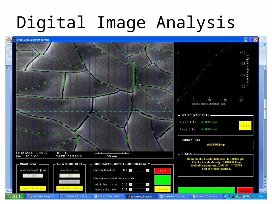
Digital Image Analysis

Analysis of Experimental Data
• Once the experimental design has been determined and the trials have been carried out, the measured performance characteristic from each trial can be used to analyze the relative effect of the different parameters
• Minitab will be used to perform statistical analysis

-0.6-0.7-0.8
0.7440.7320.7200.708
0.6960.6840.6720.660
963
321
0.7440.7320.7200.7080.6960.684
0.6720.660
170160150
Deposition Voltage (V)
Mea
n of
Mea
ns
Deposition Time (min)
Composition of Solution Deposition Temperature (oC)
Main Effects Plot for Means (Crack density & S/In Molar Ratio)Data Means

-0.600-0.625-0.650-0.675-0.700-0.725-0.750-0.775-0.800-0.825
0.105
0.090
0.075
0.060
0.045
0.030
0.015
0.000
-0.015
-0.030
Deposition Voltage (V)
Cra
ck D
ensi
ty (/
µm)
Plot of Crack Density (/µm) vs Deposition Voltage (V) with Fitted Line
-0.600-0.625-0.650-0.675-0.700-0.725-0.750-0.775-0.800-0.825
3.5
3.0
2.5
2.0
1.5
1.0
0.5
0.0
-0.5
-1.0
Deposition Voltage (V)
S/I
n M
olar
Rat
io
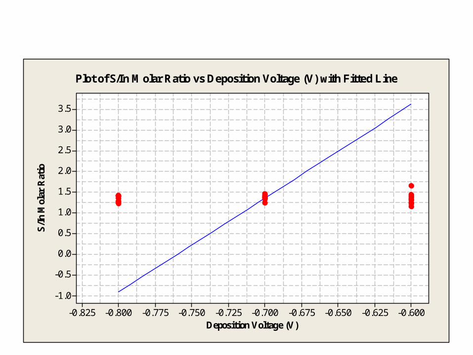
Plot of S/In Molar Ratio vs Deposition Voltage (V) with Fitted Line

Response Table for Signal to Noise Ratios
Nominal is best (10*Log10(Ybar**2/s**2))
Deposition Deposition Deposition Composition TemperatureLevel Voltage (V) Time (min) of Solution (oC)1 -2.011 -2.577 -2.466 -2.4612 -2.458 -2.368 -2.319 -2.3523 -2.704 -2.227 -2.387 -2.359Delta 0.693 0.350 0.147 0.108Rank 1 2 3 4