electronic balance for precision weighing...
TRANSCRIPT

i
UNIVERSITY OF NAIROBI
FACULTY OF ENGINEERING
DEPARTMENT OF ELECTRICAL AND INFORMATION ENGINEERING
ELECTRONIC BALANCE FOR PRECISION WEIGHING.
PROJECT INDEX: PRJ 016
BY
NJUGUNA GICHUKI SAMUEL
F17/1794/2006
SUPERVISOR: PROF. ELIJAH MWANGI
EXAMINER: DR. MBUTHIA
Project report submitted as a partial fulfillment of the requirement for the award of the degree
Of
Bachelor of Science in Electrical and Electronic Engineering of the University of Nairobi
Submitted on:
18th May, 2011

ii
DEDICATION To the almighty God, for the many gifts you have bestowed upon me, I can never thank You
enough. To my parents for teaching me valuable life lessons.

iii
ACKNOWLEDGEMENTS I gratefully acknowledge the support of my project supervisor PROF. ELIJAH MWANGI for
his great help and motivation all through my project. To all the lecturers in the department of
electrical and information engineering for instilling knowledge in us. My friends Dancan
Waiharo, Adam Olalo and Kiiru Nelson for their constructive criticism.

iv
DECLARATION AND CERTIFICATION I certify that the information presented in this report is my original effort and has not been
presented before for a degree award in this or any other university to the best of my knowledge.
………………………………………..
NJUGUNA GICHUKI SAMUEL
F17/1794/2006
Date:………………………
This report has been submitted to the Department of Electrical and Information Engineering,
University of Nairobi with my approval as supervisor:
………………………………
PROF. ELIJAH MWANGI.
Date:………………………

v
Table of Contents
DEDICATION ........................................................................................................................................ ii
ACKNOWLEDGEMENTS .................................................................................................................... iii
DECLARATION AND CERTIFICATION ............................................................................................ iv
LIST OF FIGURES ................................................................................................................................ vi
ABSTRACT .......................................................................................................................................... vii
CHAPTER 1 ........................................................................................................................................... 1
INTRODUCTION ............................................................................................................................... 1
Background ..................................................................................................................................... 1
OBJECTIVE ....................................................................................................................................... 2
MAIN OBJECTIVE ........................................................................................................................ 2
SPECIFIC OBJECTIVES ................................................................................................................ 2
PROJECT SCOPE ........................................................................................................................... 2
CHAPTER 2 ........................................................................................................................................... 3
LITERATURE REVIEW .................................................................................................................... 3
ELECTRONIC BALANCE ............................................................................................................. 3
BLOCK REPRESENTATION ......................................................................................................... 3
SENSORS ....................................................................................................................................... 4
SIGNAL CONDITIONING ............................................................................................................. 6
PROGRAMMER ........................................................................................................................... 15
PARALLEL PORT ........................................................................................................................ 15
Power supply ................................................................................................................................. 18
CHAPTER 3 ......................................................................................................................................... 19
PROJECT DESCRIPTION AND IMPLEMENTATION ................................................................... 19
DESIGNING A POWER SUPPLY .................................................................................................... 19
MOUNTING THE STRAIN GAUGE ON A STEEL RULE .......................................................... 20
DESIGNING THE SIGNAL CONDITIONING CIRCUIT ............................................................. 21
A DAPA PROGRAMMER CONNECTED TO ATmega32L INTERFACED TO THE LCD ...... 22
ELECTRONIC BALANCE DESIGN ............................................................................................ 23
DESIGNING THE SYSTEM SOFTWARE ................................................................................... 26
CHAPTER 4 ......................................................................................................................................... 35
vi
RESULTS AND DISCUSSIONS ...................................................................................................... 35
Calibration ..................................................................................................................................... 35
Output on the LCD screen ............................................................................................................. 37
CHAPTER 5 ......................................................................................................................................... 39
CONCLUSIONS ............................................................................................................................... 39
RECOMMENDATIONS AND SUGGESTIONS FOR FURTHER WORK ....................................... 39
LIST OF FIGURES Figure 1: block diagram of the electronic balance .................................................................................... 3
Figure 2 : Bonded metallic Strain Gauge .................................................................................................. 5
Figure 3: signal conditioning block representation ................................................................................... 6
Figure 4: power supply .......................................................................................................................... 19
Figure 5: mounted strain gauge .............................................................................................................. 20
Figure 6: signal conditioning circuit ....................................................................................................... 21
Figure 7.interface of the microcontroller to the LCD and DB-25 ............................................................ 23
Figure 12: LCD displaying .................................................................................................................... 33
Figure 13: Output on the LCD screen .................................................................................................... 38

vii
ABSTRACT Accuracy in weight measurement in the business world especially in the market places today has
become a crucial issue. Analog scales can measure accurately but some approximation has to be
done when the needle pointer is between two calibrated measurements. The springs also suffer
from wear and tear leading to declining accuracy. This has called for introduction of the digital
scales. This project describes the development and use of an electronic balance using the Atmel
ATmega32L microcontroller. The designed scale is to perform weight measurements to a high
degree of accuracy. A high-resolution Analog-to-Digital Converter (ADC) resident in the
microcontroller is used to accurately measure the load cell output. The measured weight is to be
in digital format and is displayed on the LCD.

1
CHAPTER 1
INTRODUCTION
Background
An electronic scale provides an excellent measurement of weight of given objects. These scales
are capable of measuring weights in an accurate manner. Unlike the conventional spring-based
measurement system these devices age gracefully rather than gradually. Digital display makes
the interpretation of the reading free from ambiguities and also the fact that these scales often
have a great look and are also easy to use.
Problem definition and Justification
The traditional scales have measured weights and served most of our purposes since time
immemorial. People have been happy with the weights to a good extent and practical problems
have been addressed using the analog weighing machines. However there are significant benefits
of using electronic weighing scales over analog ones. The primary benefits make it clear enough
why most people today have less preference to the old spring-and-needle weighing scales and
have started switching to the digital electronic system. The advantages include;
a) Accurate measurement: the electronic scale measures the weight accurately. These
scales measure weights with smaller increments compared to analog scales, thereby
significantly enhancing the accuracy. This has the advantage over analog scales that
employs delicate springs that wear out with time.
b) Accurate reading: The reading provided to the scale user is in exact grams, and not an
approximate reading left for the user to interpret based upon the movement of some
needle.
c) Heavy-duty measurements: These scales can measure heavier weights compared to
analog ones and are accurate over a higher weight range.
d) Long-term precision: Digital scales do not lose accuracy with time, unlike an ever-
loosening spring in the traditional weighing machine. So the machine reads accurately
over a long period.

2
OBJECTIVE
MAIN OBJECTIVE
The main objective of this project was to design an electronic balance for precision weighing
using foil type strain gauges and the Atmel atmega32L microcontroller and to display the result
on the LCD.
SPECIFIC OBJECTIVES
a) Mount the strain gauge on a suitable beam.
b) To design the signal conditioning circuitry for the strain gauge so that it can be used as a
measurement device.
c) Perform analog to digital conversion using the inbuilt ADC module in the
microcontroller.
d) Interface the conditioning circuitry to the microcontroller and also between the
microcontroller and the LCD.
e) Design and build a dapa (direct avr parallel access) programmer for loading the program
into the controller.
f) Develop a program using AVR studio and PonyProg2000 and load it to the
microcontroller using the dapa programmer.
g) Perform calibration of the system (weighing scale).
h) Do some weight measurements and compare them with those from a commercial scale.
PROJECT SCOPE
The Atmega32L based electronic balance was to be used to measure weights between 0 and 1 kg
and display the mass on the LCD. The high resolution of the 10 bit ADC resident in the
microcontroller enables the measuring with a sensitivity of 1 gram for every 4.833mv.

3
CHAPTER 2
LITERATURE REVIEW
ELECTRONIC BALANCE
The sensing element is placed as one arm of the Wheatstone bridge. With no load on the sensing
element the bridge is balanced. On placing some load on the sensing element , the resistance of
the sensing element changes causing some imbalance of the bridge resulting in some output
voltage in the order of a few milivolts. The small signal is then amplified using suitable
amplifiers to levels compatible to the analog to digital converters. The ADC converts the analog
signal to a digital format which is required by the microprocessor, for precision measurements a
high resolution ADC is employed. The data sent is read by a microprocessor and is finally
displayed on a suitable display device such as a seven segment display or the LCD. The above
constitute the building blocks of the electronic balance.
BLOCK REPRESENTATION
LCD DISPLAY
MICROCONTROLLER
ANALOG TO DIGITAL
CONVERSION
SIGNAL CONDITIONING
SENSOR
Figure 1: block diagram of the electronic balance

4
SENSORS
A sensor is a device that receives a signal or a stimulus and responds with an electrical signal.
Sensors and their associated circuits are used to measure various physical properties such as
temperature, force, pressure, flow, position, light intensity and others. These properties act as
stimulus to the sensor, the sensor output has to be conditioned and processed to provide the
corresponding measurement of the physical property.
Sensors are usually part of a larger system consisting of signal conditioners and various analog to
digital signal processing circuits. The system can be a measurement system, data acquisition
system or process control system.
Sensors may be classified as active or passive. An active sensor requires an external source of
excitation. These comprise of resistor-based sensors such as thermistors, resistance temperature
detectors (RTDS) and strain gauges. They are called active because a current must be passed
through them and the corresponding voltage measured to determine the resistance value.
Passive sensors on the other hand generate their own electrical outputs signals without requiring
any external excitation. Passive sensors include thermocouples and photodiodes which generate
thermoelectric voltages and photoelectric currents respectively.
Another logical way to classify sensors may be by the physical property that the sensor is
designed to measure. This means grouping them as pressure sensors, temperature sensors, force
sensors and motion sensors. It is however important to note that sensors that measure different
physical properties may have the same type of electrical output. An example is the strain gauge
and RTDS. [REF. 3]
STRAIN GAUGE AS A SENSOR
A strain gauge is a conducting wire whose resistance changes by a small amount when it is
lengthened or shortened. Strain gauges are made from metal alloy such as constantan, nichrome
V or platinum alloy. For high temperature work they are made of wire. For moderate temperature
applications they are made by forming the metal alloy into very thin sheets by a photo etching

5
process, the resultant product is called a foil type strain gauge. The strain gauge can be used can
be used as a sensor for pressure, force, torque, and as a position sensor.
The majority of strain gauges are foil type available in a wide range of shapes and sizes to suit a
variety of applications. They operate on the principle that as the foil is subjected to stress the
resistance of the foil changes in a defined way. The metallic strain gauge consists of a metallic
foil arranged in a grid pattern. This grid pattern maximizes the the amount of metallic wire
subject to strain in the parallel direction. The cross-sectional area of the grid is minimized to
reduce the amount of shear strain. The grid is bonded into a thin backing which is attached
directly to the test specimen. This implies that the strain experienced by the test specimen is
transferred directly to the strain gauge which responds with a linear change in electrical
resistance.
Figure 2 : Bonded metallic Strain Gauge
A fundamental parameter of the strain gauge is its sensitivity to strain expressed quantitavely as
the gauge factor (GF). Gauge factor is defined as the fractional change in the electrical resistance
to the fractional change in length.
GF= (∆R/R)/ (∆L/L)
The ratio ∆L/L is called unit strain. [REF. 1].
It is important to note that the resistance change for the gauge for the full force range is small,
thus to use the gauge as a measurement device calls for a way of measuring very small resistance

6
changes with high accuracy. Such precisition measurement applications call for the use of a
bridge measurement circuit. The wheat-stone bridge is therefore employed.
SIGNAL CONDITIONING
Conditioning the signal means that some characteristic of the signal is being changed. Strain
gauge measurement involves sensing extremely small resistance changes with high accuracy.
This means that there must be proper selection and use of the bridge, good signal conditioning,
reliable wiring and data acquisition.
Signal conditioning includes;
a) Bridge completion.
b) Excitation.
c) Amplification.
d) Filtering.
e) Bridge balancing.
Signal conditioning is primarily utilized for data acquisition in which sensor signals must be
normalized and filtered to levels suitable for analogue to digital conversion so that they can be
applied to processors.
Whatever form conditioning takes circuitry and performance is governed by the electrical
characteristic of the sensor and its output. Factors such as sensitivity, voltage and current levels,
linearity, maximum electrical ratings and stray impedances can spell the difference between a
substandard and a successful application of the device. To some degree some sensor outputs are
FILTERING (LPF) AMPLIFICATION BRIDGE COMPLETION
Figure 3: signal conditioning block representation

7
non-linear with respect to the applied stimulus and as a result their outputs must be linearized in
order to yield correct output.
Bridge completion
A simple method of measuring resistance is to force a constant current through the resistive
sensor and measure the voltage output. Any change in current will be interpreted as a resistance
change.
The wheat-stone bridge offers an attractive alternative for measuring small changes in resistance
accurately. It consists of four resistors, a source of excitation voltage and a voltage detector
connected across the other diagonal. The strain gauge is used as one arm of the bridge ( quarter
bridge circuit) and the output voltage change is an indication of the resistance change.
The sensitivity of the bridge is the ratio of the maximum expected change in the output voltage
to the excitation voltage.
Bridge sensitivity= (full-scale bridge output) / (excitation voltage).
Since more than one arm of the bridge can be made variable, sensitivity increases as more
elements are made variable. This also implies that the bridge output can be increased by
improving the sensitivity of the bridge, i.e. the bridge output can be doubled by doubling the
number of the working gauges.
An unfortunate characteristic of the strain gauge is its resistance change with temperature. This
means that the bridge may be unbalanced even when the gauge is unstrained giving an output.
This can be alleviated by using a “dummy gauge “ to cancel the effects of temperature. power
dissipation in the resistive sensor must be kept low so that self heating does not produce errors.
Excitation voltages
Although large excitation voltages yield proportionally larger full-scale output voltages, they
also result in higher bridge power dissipation and thus raise the possibility of sensor resistor self-
heating errors. On the other hand low values of excitation voltages require more gain in the

8
conditioning circuit and also increase susceptibility to low level errors such as noise and offset
voltages.
The stability of the excitation voltage or current is also an important factor to consider. This is
accomplished by designing a regulated power supply to be the excitation voltage.
Amplification
The output of strain gauges and bridges are relatively small. For a bridge whose sensitivity is
10mv/V the full-scale output with an excitation voltage of 10V is 100mv which is still small.
This calls for the use of amplifiers to boost the signal level, increase the measurement resolution
and improve the signal to noise ratio.
The output of a single element varying bridge may be amplified using a single varying op-amp,
this method although attractive has poor overall performance. This is because the RF resistor
must be chosen carefully and matched to maximize the common mode rejection. It is difficult to
maximize common mode rejection while at the same time allowing different gain options since
gain depends on the bridge resistances and RF.
The differential amplifier has better performance than the single input amplifier. For the single
input amplifier noise voltages act as if they are in series with the input signal, this means that
both the noise voltages and the input signal are amplified equally. This may be undesirable
where the noise voltage level is equal to or greater than the input signal. For the differential
amplifier case the noise voltage is not amplified and is therefore eliminated from having any
significant effect on the output voltage. This condition is guaranteed as long as the resistors are
matched. The two disadvantages of the basic differential amplifier are low input impedance and
changing gain. The first disadvantage is eliminated by buffering (isolating the inputs with
voltage followers). The gain can be adjusted by one resistor. The setback of this buffered
differential amplifier is that it can only drive floating loads.
A much better approach to amplify the bridge output is to use an instrumentation amplifier, the
instrumentation amplifier has better gain accuracy usually and high common mode rejection
ratio.

9
Instrumentation amplifier
An instrumentation amplifier is a type of differential amplifier that has been outfitted with input
buffers, which eliminate the need for input impedance matching and thus make the amplifier
particularly suitable for use in measurement. Additional characteristics include very low DC
offset, low drift low noise, very high open-loop gain, very high common rejection ratio and very
high input impedances. Instrumentation amplifiers are used where great accuracy and stability of
the circuit both short- and long-term are required. The electronic instrumentation amp is almost
always internally composed of 3 op-amps. These are arranged so that there is one op-amp to
buffer each input, and one to produce the desired output with adequate impedance matching for
the function. The instrumentation amplifier is preferred for bridge amplification because of its
stable gain and high common mode rejection. In this project the µa725 instrumentation amplifier
was used.
Filtering
Filters are used to separate signals passing those of interest and attenuated the unwanted
frequencies. In data conversion, filters are mostly used to eliminate aliasing in A/D systems.
Filters are mostly employed after the signal has been amplified to increase its amplitude. Then a
selection of particular signal frequencies is accomplished by passing the signal through a
frequency selection filter. A low pass filter was employed before the signal was applied to the
analog to digital converter (ADC).
Analog to digital conversion
Once the signal has been amplified it is taken to the ADC module of the microcontroller. A
microcontroller is used to process information from the natural world, decide on the course of
action based on the information collected and then issue control signals to implement the
decision. Since the signal from the sensor is analog in nature and the controller is a digital
processor therefore an analog to digital converter is required.

10
Converter performance is important and maintaining that performance in a system application is
important. When dealing with low level signals and low frequency applications resolution is an
important factor.
Resolution = 2^n where n is the no of digital outputs.
Increasing the no of bits results in a finer resolution and therefore reduces the quantization error
where the quantization error is the difference between the the input analog signal and the
quantized digital value. ADCs must also have a wide dynamic range, high sampling frequencies
and generally excellent ac specifications. Other desirable characteristics include, low power,
single supply operation, low cost and smaller input/output signal swings.
ADC conversion technologies
The four different types of technologies used in ADCs are the successive approximation
conversion, the integration conversion, the counter-based conversion, and the parallel
conversion.
Successive Approximation
The successive approximation technique uses a DAC, a controller, and a comparator to perform
the ADC process. Starting from the MSB down to the LSB, the controller turns on each bit at a
time and generates an analog signal, with the help of the DAC, to be compared with the original
input analog signal. Based on the result of the comparison, the controller changes or leaves the
current bit and turns on the next MSB. The process continues until decisions are made for all
available bits.
Integration
The integration technique uses an integrator, a comparator, and a controller to convert analog
signals to digital signals. A sampled analog signal is integrated over a fixed period, say n clock
cycles of the digital system. Another fixed reference signal is integrated over time and compared
with the input analog signal integrated. Although the value of the reference signal integrated is
smaller than the input analog signal integrated, the reference signal is continuously integrated,
and the time for the integration is measured. When the two integrated values equal, the measured
time is converted to a digital encoded value.

11
Counter-Based Conversion
This conversion is performed with the help of a counter, a DAC, and a comparator. The counter
starts at 0 and counts up. As the counter counts up, the corresponding value is converted to an
analog value and compared with an input analog signal. As long as the input analog signal is
greater than the signal generated by the DAC, the counter counts up and the process continues.
The Atmega32L ADC module uses the successive approximation technique. After the signal
has been converted to digital format it is applied to the microcontroller for processing so that it
can be successfully displayed. [REF. 2]
MICROPROCESSOR A microprocessor is a device that receives data or information processes it in accordance with a
stored software program and outputs signals in digital form. It accesses memory units, fetches
instructions and executes them, performs arithmetic and logical calculations, monitor external
events, keep track of where information is to go and controls timing and operation sequence. The
main constituents of a microprocessor are;
- Central processing unit (CPU).
- Primary memory that include RAM and ROM.
- Input and output interfaces to handle communication the microprocessor and the outside
world.
The advantage of the microprocessor in circuit design is that one can change functionality by
changing the software while keeping the hardware the same. This reduces the cost of production
since different systems can use the same hardware base.
Microprocessors can be categorized into several architectural forms namely;
- Von-Neumann architecture
- Harvard architecture
- CISC and RISC architecture
Microcontrollers based on Von-Neumann architecture have a single data-bus that is used fetch
both instructions and data program. Instruction and data are stored in a common main memory.
When addressing main memory, the controllers first fetches an instructions and then it fetches
data to support the instructions. The two separate fetches slow down the controller operation.
Microcontrollers based on Harvard architecture have a separate data bus and instruction bus. An
instruction is pre-fetched while the current instruction is being executed. Once the current

12
instruction is completed, the instruction is ready to be executed. This pre-fetch allows for faster
execution of instruction than the Von-Neumann architecture.
CISC - processors have a bigger instruction set with many addressing modes. It has an easy
compiler design but decoding of an instruction is complex and execution time is much slower.
An example is the Intel 8086.
RISC - processors have a smaller instruction set with few addressing mode. It has a complex
compiler design but its executions are faster. An example is the Intel 8085.
In this project I used the Atmel AVR Atmel ATmega32L. The AVR is a modified Harvard
architecture 8 bit RISC single chip which was developed by Atmel co-operation in 1996. The
AVR was one of the first microcontroller’s families to use on-chip flash memory for program
storage as opposed to one time programmable ROM, EPROM or EEPROM.
Some of the reasons why the Atmel ATmega32L is preferred include;
- High performance coupled with low power consumption.
- Outstanding flash memory technology.
- Reduced instruction set computer Harvard architecture.
- Single cycle execution.
- Wide variety of operating voltages (1.8V-5.5V).
- Architecture designed for C language.
- One set of development tools for the entire AVR line.
- In system programming, debugging and verification.
In this project the Atmel ATmega32L microcontroller was used mainly because it has an inbuilt
ADC module, internal selectable RC oscillator and the ability to support in system programming
(ISP).
The Atmel ATmega32L
The ATmega32L provides the following desirable features: 32Kbytes of In-System
Programmable Flash Program memory with Read-While-Write capabilities, 1024bytes
EEPROM, 2Kbyte SRAM, 32 general purpose I/O lines, 32 general purpose working registers,
On-chip Debugging, support and programming, three flexible Timer/Counters with compare
modes, Internal and External Interrupts, a serial programmable USART, a byte oriented Two-

13
wire Serial Interface, an 8-channel, 10-bit ADC with 8 single ended channels, a programmable
Watchdog Timer with Internal Oscillator, an SPI serial port, and six software selectable power
saving modes that include the Idle mode , the Power down mode ,Power-save mode , the ADC
Noise Reduction mode , In Standby mode and extended Standby mode.[datasheet]
ATmega32L pin description
VCC- Digital supply voltage.
GND- Ground.
Port A (PA7-PA0) - Port A serves as the analog inputs to the A/D Converter.
Port A also serves as an 8-bit bi-directional I/O port, if the A/D Converter is not used. The PortA
output buffers have symmetrical drive characteristics with both high sink and source capability.
Port B (PB7-PB0) - Port B is an 8-bit bi-directional I/O port with internal pull-up resistors
(selected for each bit). The Port B output buffers have symmetrical drive characteristics with
both high sink and source capability.
Port C (PC7-PC0) - Port C is an 8-bit bi-directional I/O port with internal pull-up resistors
(selected for each bit). The Port C output buffers have symmetrical drive characteristics with
both high sink and source capability. As inputs, Port C pins that are externally pulled low will
source current if the pull-up resistors are activated.
Port D (PD7-PD0) - Port D is an 8-bit bi-directional I/O port with internal pull-up resistors
(selected for each bit). The Port D output buffers have symmetrical drive characteristics with
both high sink and source capability. As inputs, Port D pins that are externally pulled low will
source current if the pull-up resistors are activated.
RESET- Reset Input. A low level on this pin for longer than the minimum pulse length will
generate a reset, even if the clock is not running.
XTAL1 - Input to the inverting Oscillator amplifier and input to the internal clock operating
circuit.
XTAL2 - Output from the inverting Oscillator amplifier.
AVCC - AVCC is the supply voltage pin for Port A and the A/D Converter. It should be
externally connected to VCC, even if the ADC is not used. If the ADC is used, it should be
connected to VCC through a low-pass filter.
AREF - AREF is the analog reference pin for the A/D Converter.

14
Time base
The microcontroller is a complex synchronous state machine. It responds to program steps in a
sequential manner as dictated by a user-written program. The microcontroller executes a
command through a predictable fetch, decode and execute sequence. The speed at which a
microcontroller performs these actions is controlled by a precise time base called the clock. The
clock source is routed throughout the microcontroller to provide a time base for all peripheral
subsystems. The ATmega32L may be clocked internally, using a user-selectable resistor
capacitor (RC) time base, or externally using a crystal. The RC internal time base is selected
using programmable fuse bits. One may choose an internal fixed clock operating frequency of 1,
2, 4, or 8 MHz To provide for a wider range of frequency selections, an external oscillator may
be used. The external time sources, in order of increasing accuracy and stability, are an external
RC network, a ceramic resonator, or a crystal oscillator. [REF. 2].
Serial Communications
When choosing controllers to be used for various applications and circuits it is important to
consider the various communications subsystems that the controller is equipped with and even to
consider how to load a program in the controller.
The ATmega32L is equipped with a host of different serial communication subsystems,
including the Universal Synchronous and Asynchronous Serial Receiver and Transmitter
(USART), the Serial Peripheral Interface (SPI), and the Two-Wire Serial Interface (TWI). What
all of these systems have in common is the serial transmission of data. In a serial
communications transmission scheme, data are sent a single bit at a time from transmitter to
receiver.
Serial USART - The serial USART is used for full duplex (two-way) communication between a
receiver and transmitter. This is accomplished by equipping the ATmega32L with independent
hardware for the transmitter and receiver. The USART is typically used for asynchronous

15
communication. To maintain synchronization between the transmitter and receiver, framing start
and stop bits are used at the beginning and end of each data byte in a transmission sequence.
Two-Wire Serial Interface - The TWI subsystem allows the system designer to network a number
of related devices (microcontrollers, transducers, displays, memory storage, etc.) together into a
system using a two-wire interconnecting scheme. The TWI allows a maximum of 128 devices to
be connected together.
Serial Peripheral Interface - The SPI may be viewed as a synchronous 16-bit shift register with
an 8-bit half residing in the transmitter and the other 8-bit half residing in the receiver. The
transmitter is designated the master because it provides the synchronizing clock source between
the transmitter and the receiver. In the SPI system, the transmitter and receiver share a common
clock source.
The serial peripheral interface (SPI) method of communication was employed to send code to the
ATmega32L. This was accomplished using a dapa (direct avr parallel acces) programmer and a
PC with a parallel port.
PROGRAMMER
A programmer is a hardware device that downloads (writes) code onto the controllers ROM or
Flash memory. the code is written and compiled using suitable software , the executable set of
instructions obtained are sent to the controller using either the parallel port ,serial port or USB
port using various programmers.
A popular method to program a controller is to use in system programming (ISP). The Atmel
Avr line of controllers support ISP ,this allows one to test and debug code without interfering
with the hardware set up every time one needs to write a new version of code. Programmers that
use ISP tend to be cheaper and simpler compared to methods like parallel or high voltage
programming. For this project a dapa programmer was used (direct avr parallel access). When
using ISP the data is send serially even though the port being used is the parallel port.
PARALLEL PORT
Parallel Port interfacing is the simplest method of interfacing. Parallel Port’s are standardized
under the IEEE 1284 standard first released in 1994. It has data transfer speed up to 1Mbytes/sec.

16
Parallel port is basically the 25 pin Female connector (DB-25) in the back side of the computer
(Printer Port). It has 17 input lines for input port and 12 pins for output port. Out of the 25 pins
most pins are Ground and there is data register (8 bit), control register (4 bit) and status register
(5 bit).
The following Pins of the parallel port are used -
Table 1: DB25 – pins used for serial communication
Pin No. Description
7,8,9 Data pins
10 Status pin
19 Ground
After the program has been sent to the controller the next step is to interface the controller with
an output device such as a display device. Display devices available today include LEDs seven
segment displays and LCDs.
Display devices
A number of display devices are available today as output devices, these are;
a) LEDs.
b) Seven segment displays.
c) LCDs
In this project the LCD display was used.
LCD display
LCDs are used as output devices to display text information. A 16x2 LCD is the most common
and has the capability of displaying 2 lines of 16 characters. Data paths and control lines are
required between the LCD and the microcontroller. A small controller mounted on the back
panel of the LCD translates the ASCII characters and control signals to properly display the
characters.

17
LCD consists of rod-shaped tiny molecules sand- witched between flat pieces of glass and an
opaque substrate. The rod shaped molecules align into different positions based on the electric
charge applied to them. Light passing through makes the desired images appear. In recent times
the LCDs have found popularity replacing LEDs and seven segment displays. This is due to;
a) Ability to display numbers characters and graphics.
b) They are thin and flat.
c) They consume very little amount of power.
d) The declining prices of LCDs.
e) Presence of a refreshing controller in the LCD relieving the CPU the task of refreshing.
The HD44780U standard allows for easy communication with the majority of LCDs regardless
of their manufacturer. The control chip receives data from the external source and communicates
directly to the LCD. This standard requires three control lines and 4 or 8 I/O lines.
The enable line (EN) - This line is used to indicate the start of a transmission of a data byte to
the LCD controller. To indicate the start of transmission, this line is brought high. When
transmission is complete, the EN line is brought low.
The register select line (RS) - This line indicates to the LCD controller whether the data byte is to
be treated as a command or as text data to be displayed on the screen. If the RS line is high, the
data byte is treated as text to be displayed. If the RS line is low, the data byte is treated as a
command.
The read/write line (RW) - When this line is low, the information on the data bus is written to the
LCD controller. If this line is high, the LCD controller can be read to check the status of the
LCD.
Every electronic circuit is designed to operate with some supply voltage which is usually
assumed to be constant. If the supply is not constant unpredictable happenings may occur to the
microcontroller and their associated circuits. This makes a power supply a very crucial part of
any electronic circuit.

18
Power supply
In normal operation, microcontrollers and their associated circuits are sourced by a regulated and
somehow stabilized power supply. Whenever in such cases the supply voltage is below the
minimum specified level, the microcontroller's behavior cannot be predicted, which can lead to
critical situations of the application. Unwanted effects include:
- Wrong execution of the application program.
- Outputs changing state.
- Unintended accesses to internal or external memory.
A voltage regulator provides this constant DC output voltage and contains circuitry that
continuously holds the output voltage at the design value regardless of changes in load current or
input voltage. The LM7805 and regulator was used in this project to design a regulated power
supply for the circuit.

19
CHAPTER 3
PROJECT DESCRIPTION AND IMPLEMENTATION
DESIGNING A POWER SUPPLY
A regulated power supply was designed due to the fact that a.c line voltage suffers from
considerable variations which may result in variations in the power supply output voltage. This
varying voltage is not healthy for the proper operation of the microcontroller and other
components of the circuit. Thus the LM7805 regulator was used to design a 5V power supply.
A transformer was used to step down the 240V ac to 12V ac. A rectifier was then employed to
convert the ac voltage to dc. A full wave rectifier was made using the IN4001 diodes and then a
100uf capacitor was used for smoothening. The output capacitor was made to be 10uf.
The output of the rectifier was then connected to the LM7805 regulator. The output voltage is
thus stable regardless of the load variations or variations in the ac input voltage from the mains.
The LM7805 regulator employs internal current limiting, thermal shutdown and safe area
compensation making them essentially indestructible.
Diode D5 is a protection diode connected output to input. If the input voltage is accidentally
shorted to ground the input is pulled to ground potential while the output remains near the initial
output voltage due to stored charge in the output capacitor. This diode thus shunts most of the
capacitors discharge current around the regulator to ground.
Figure 4: power supply
TR1
TRAN-2P2S
BR1
DF02M
VI1 VO 3
GN
D2
U17805
D5
DIODE
C1100u
C210u
R1470R
D1LED

20
MOUNTING THE STRAIN GAUGE ON A STEEL RULE
The strain gauge is a sensitive sensor and proper and careful handling during mounting was
observed so as not to damage the sensor and make it unusable. The following procedure was
observed;
- Cutting the gauge to size – the gauge was cut to size using a new blade as recommended
- Cleaning and preparing the sensor block – the surface of the steel rule was scrubbed using
rough sand paper and then softened using a soft sand paper. The surface was then wiped using a
clean sponge.
- A suitable adhesive (super glue) was then used to mount the gauge on the clean surface with
the foil type side up.
- The terminals of the strain gauge were soldered on the steel rule to avoid the contacts
weakening or being loose or even breaking from the gauge.
- The gauge resistance was then measured to ensure that its resistance is 120 ohms and its
resistance has not been tampered with.
Figure 5: mounted strain gauge

21
DESIGNING THE SIGNAL CONDITIONING CIRCUIT
The balanced bridge circuit was designed so as any change in the gauge resistance can unbalance
the bridge and cause a voltage change which can then be amplified and make it suitable to be
used for measurement purposes.
The ua725 instrumentation amplifier was used due to its high common mode rejection ratio, low
input offset current and low input voltage drift. The instrumentation amplifier was used to boost
the signal level to levels compatible to analog to digital converters, amplification also improves
the measurement resolution and signal to noise ratio.
Figure 6: signal conditioning circuit
R1330R
R3330R
R41M
R510k
R610k
RV1
POT
R71M
R81M
3
26
74 1 5
U1
741
R9120R
R10120R
R11470R
C1100u

22
A dapa programmer connected to Tmega32L interfaced to the LCD
This simple programmer is a parallel port interface programmer. This programmer uses the
parallel port of the PC to communicate with the controller.
Requirements include male DB_25 and connecting wires.
The pins of male DB-25 and Atmega32L were connected as below.
Table 2: pins of DB25 corresponding to those of ATmega32L
DB-25 ATMEGA32L
7 RESET (9)
8 SCK (8)
9 MOSI(6)
10 MISO(7)
18 GND(18)
The parallel port is a very sensitive device, the power supply should never exceed 5V. for
additional protection 1k resistors were used on SCK,MOSI and MISO wires.
a) SCK (Serial clock) - This is used for synchronization between the PC and the
microcontroller.
b) MOSI (master out slave in) – the master refers to the pc and the slave is the controller this
line is used by the pc to send data to the controller.
c) MISO (master in slave out) – Used for verifying the code on the chip.
d) RESET – This is used to reset the controller to signal the start of transmission.
e) GND – A common ground connection.

23
Figure 7.interface of the microcontroller to the LCD and DB-25
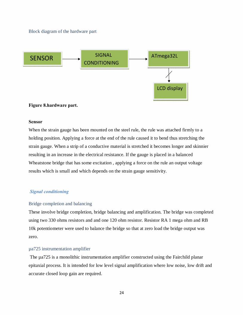
ELECTRONIC BALANCE DESIGN
The electronic balance was made up of two parts the hardware part and the software part.
Hardware part
This involved putting together all the individual parts that had previously been designed and
doing a good interface to come up with the whole unit. The parts were the sensor, signal
conditioning circuit ,the microcontroller and the LCD display.
PA0/ADC040
PA1/ADC139
PA2/ADC238
PA3/ADC337
PA4/ADC436
PA5/ADC535
PA6/ADC634
PB0/XCK/T01
PB1/T12
PB2/INT2/AIN03
PB3/OC0/AIN14
PB4/SS5
PB5/MOSI6
PB6/MISO7
PB7/SCK8
PA7/ADC733
RESET9
XTAL113
XTAL212
PC0/SCL 22
PC1/SDA 23
PC2/TCK 24
PC3/TMS 25
PC4/TDO 26
PC5/TDI 27
PC6/TOSC1 28
PC7/TOSC2 29
PD0/RXD 14
PD1/TXD 15
PD2/INT0 16
PD3/INT1 17
PD4/OC1B 18
PD5/OC1A 19
PD6/ICP 20
PD7/OC2 21
AVCC 30
AREF 32
U1
ATMEGA32
D714D613 D512 D411 D310D29 D18 D07
E6 RW5RS4
VSS1
VDD2
VEE3
LCD1
LM016L
C1100n
RV1POT
R110k
SW1SW-SPST-MOM
11421531641751861972082192210231124122513
J1
CONN-D25M
24
Block diagram of the hardware part
Figure 8.hardware part.
Sensor
When the strain gauge has been mounted on the steel rule, the rule was attached firmly to a
holding position. Applying a force at the end of the rule caused it to bend thus stretching the
strain gauge. When a strip of a conductive material is stretched it becomes longer and skinnier
resulting in an increase in the electrical resistance. If the gauge is placed in a balanced
Wheatstone bridge that has some excitation , applying a force on the rule an output voltage
results which is small and which depends on the strain gauge sensitivity.
Signal conditioning
Bridge completion and balancing
These involve bridge completion, bridge balancing and amplification. The bridge was completed
using two 330 ohms resistors and and one 120 ohm resistor. Resistor RA 1 mega ohm and RB
10k potentiometer were used to balance the bridge so that at zero load the bridge output was
zero.
µa725 instrumentation amplifier
The µa725 is a monolithic instrumentation amplifier constructed using the Fairchild planar
epitaxial process. It is intended for low level signal amplification where low noise, low drift and
accurate closed loop gain are required.
SIGNAL CONDITIONING
SENSOR ATmega32L
LCD display

25
Considering that the output of the bridge is in the order of a few milivolts, the instrumentation
amplifier was used to raise the signal level so that it can be useful for measurements applications.
The µa725 is lead compatible to the µa741 and has other desirable characteristics such as ;
- High common mode rejection ratio – 120 db.
- High input voltage range - ±14V
- Wide power supply range - ±3V to ±22V
Once the signal has been amplified the signal must first be passed through a low pass filter
before it can be applied to a data conversion device. The low pass filter removes noise that may
have been added during signal amplification.
ATmega32L ADC module
The ADC feature available on PORTA of the ATmega32L is powerful and flexible and has the
following desirable characteristics;
- 10 bit resolution.
- 2 LSB absolute accuracy
- 13 ADC clock cycle conversion time.
- 8 multiplexed single ended channels.
- Selectable right or left justification.
- 0 to VCC ADC voltage range.
The full-scale input voltage range of the ADC is generally determined by the reference voltage
VREF. The reference voltage (maximum) value can be taken from the AREF pin or an internal
reference level of 2.56V which is provided and which can be accessed via the software. The
AVCC may also be used as AREF by simply decoupling It (connecting to ground through a
capacitor). The reference voltage was selected to be 5V.
Since 10-bit resolution is available. This means that you can distinguish between two readings
which have a difference of value equal to the resolution. This means that the max value is broken
up into 1024 parts and for our reference voltage of 5V, the resolution is 4.88mV. The absolute
accuracy was therefore found to be 9.76mv.
The ADC can be used in free running mode(which means it will keep on converting
continuously) or single conversion mode. An interrupt may be generated once a conversion is
complete, so that the MCU need not keep on checking for completion of conversion.

26
There is a ADC Noise Cancelling mode, which allows the user to switch off the other digital
circuitry which might affect the conversion.
Since the result is 10 bit, the result is stored in 2 registers, ADCH and ADCL. If the ADLAR bit
is not set, the result is right aligned. In that case, the 2 MSBs of the result are the 2 LSBs of the
ADCH register and the remaining 8 LSBs of the result are in the ADCL. In this case, it is
necessary to read the ADCL first and the ADCH second, only then will the ADC registers be
updated with the next result.
Accuracy of the ADC result depends on the prescaler setting, its best between 50 and 200 KHz
clock frequency. Running at 8 MHz the prescaler was set as 64, which gives a clock frequency of
8/64, which is 125 KHz.
DESIGNING THE SYSTEM SOFTWARE
The software tools used were;
a) WinAVR– WinAVR is open source package in which two sub-programs are used,
Programmers Notepad & Mfile.
b) AVR STUDIO
c) PONYPROG2000
The system program was written in C language in the programmers’ notepad in WinAVR
and the compiling and debugging done in AVRstudio. AVRstudio was set to generate a Hex
file when the program was run.
Burning code to the ATmega32L
The programmer circuit pins of parallel port have to interface with pins of ATmega32L
microcontroller which are responsible for in-system programming as described above. The
generated hex file was burnt into the microcontroller using the dapa programmer and the
Ponyprog2000. The controller was placed in the veroboard and the programmers pins and the

27
controllers pins connected as described above. The hex file was then opened in PonyProg2000
and a write command issued.

28
PROGRAM FLOW CHARTS AND DISCUSSION
START
LCD INITIALIZE
DISPLAY A WELCOME MESSAGE
ADC INITIALIZE
PERFOM ADC CONVERSION
WAIT FOR CONVERSION
DISPLAY RESULT ON LCD SCREEN
CONVERT ADC RESULT TO WEIGHT
Figure 9: the whole program flow chart

29
ADC INITIALIZE FLOW CHART
Clear the conversion
Wait for conversion to complete
PERFOM A DUMMY CONVERSION
SET ADC PRESCALER
SELECT CHANNEL
Figure 10: ADC initialization

30
ADC CONVERSION
SELECT CHANNEL
READ ADC RESULT IN EITHER ADCH OR ADCL
DO LEFT OR RIGHT ADJUST AND STORE RESULT IN ADCH OR ADCL
SET ADC PRESCALER
WAIT FOR CONVERSION
START ADC CONVERSION
Figure 11: ADC conversion

31
ADC initialization and conversion flow chart analysis
The key registers for the ADC system are ADC Multiplexer Selection Register (ADMUX), ADC
Control and Status Register A (ADCSRA) and ADC Data Registers (ADCH and ADCL).
ADC Multiplexer Selection Register (ADMUX) - The ADMUX register contains the ADLAR
bit to select left or right justification and the MUX[4:0] bits to determine which analog input will
be provided to the ADC for conversion. The REFS [1:0] bits of the ADMUX register are also
used to determine the reference voltage source for the ADC system.
ADC Control and Status Register A (ADCSRA) - The ADCSRA register contains the ADC
Enable (ADEN) bit. This bit is the ‘‘on/off’’ switch for the ADC system. The ADC is turned on
by setting this bit to a logic 1. The ADC Start Conversion (ADSC) bit is also contained in the
ADCSRA register. Setting this bit to logic 1 initiates the ADC. The ADCSRA register also
contains the ADC Interrupt flag (ADIF) bit. This bit sets to logic 1 when the ADC conversion is
complete. The ADIF bit is reset by writing a logic 1 to this bit.
ADC Data Registers (ADCH and ADCL) - The ADC Data Register contains the result of the
ADC. The results may be left (ADLAR=1) or right (ADLAR=0) justified.
Select channel - The ADC is equipped with a single successive approximation converter. That
means that only a single ADC channel may be converted at a given time. The input of the ADC
is equipped with an eight-input analog multiplexer. The analog input for conversion is selected
using the MUX [4:0] bits in the ADC Multiplexer Selection Register (ADMUX).
Set ADC prescaler – The ADC requires 13 analog-to-digital clock cycles to perform an ADC
conversion. The ADC system may be run at a slower clock frequency than the main
microcontroller clock source. The main microcontroller clock is divided down using the ADC
Prescaler Select (ADPS [2:0]) bits in the ADC Control and Status Register A (ADCSRA).
Perform a dummy conversion – The first ADC conversion value is not accurate and should be
discarded. The next consecutive values are accurate.
Read ADC result - The 10-bit result from the conversion process is placed in the ADC Data
Registers, ADCH and ADCL. These two registers provide 16 bits for the 10-bit result.

32
FLOW CHART ANALYSIS OF THE LCD MODULE
LCD INITIALIZE
Set LCD to 4 bit or 8 bit mode
Display a welcome message
Write command to command register (clear LCD)
Write data byte to data register
Figure.12. LCD initialization

33
DISPLAYING THE ADC RESULT ON LCD
LCD flow chart analysis
The three control lines are enable(EN), read/write(RW) and register select(RS).
The Enable line (EN) - This control line is used to tell the LCD that we are sending it data. To
send data to the LCD, our program should make sure this line is low (0) and then set the other
two control lines and/or put data on the data bus. When the other lines are completely ready,
bring EN high (1) and wait for the minimum amount of time required by the LCD (delay), and
end by bringing it low (0) again.
Set RW to low (to write to LCD)
Send a low to high pulse on the enable pin
Select command (RS=0) or instruction (RS=1) registers
Give a delay to enable the LCD to Interpret the instructions
Display instruction or command
Figure 8: LCD displaying

34
The Register Select line (RS) - When RS is low (0), the data is to be treated as a command or
special instruction (such as clear screen, position cursor, etc.). When RS is high (1), the data
being sent is text data which should be displayed on the screen.
The Read/Write control line (RW) - When RW is low (0), the information on the data bus is
being written to the LCD. When RW is high (1), the program is effectively querying (or reading)
the LCD. Only one instruction ("Get LCD status") is a read command. All others are write
commands so RW will almost always be low.
The LCD was set to 4 bit mode and therefore only four of the 8 data lines were used.

35
CHAPTER 4
RESULTS AND DISCUSSIONS
Calibration Table 3: Test 1
Weight in grams ADC value
50 211
100 213
150 217
200 226
250 243
300 255
A graph of adc value vs weight in grams
200
205
210
215
220
225
230
50 100 150 200
ADC
VALUE
weight
Series1

36
Table 4: Test 2
Weight in grams Adc value
50 212
100 218
150 224
200 236
250 241
300 255
The above variations may have been due to the fact that once the rule was stretched by the
weight being applied it never went back to its original position.
The sensor used was also locally mount and not accurate enough leading to some non-linearity in
the bridge output.
0
50
100
150
200
250
300
50 100 150 200 250 300
adc
value
weight
Series1

37
The gradient of the graph plotted using the results of test 2 was determined and used to calibrate
the scale.
Adc_value=M x weight +207
Weight=(adc_value -207)/M
Where M is the gradient and from the best line of fit it was found to be 2.
A comparison of the scale and a commercial one
Commercial scale Designed scale
250 252
200 207
150 157
100 103
50 45
The variations of the result from the real values may have been caused by;
a) When weight is applied on the beam the beam never comes back to the original position.
b) Vibrations on the beam as weights are applied.
c) The non-linearity of the strain gauge sensor.
d) Temperature effects since only one sensor was employed and there was no temperature
compensation.
Output on the LCD screen

38
Figure 9: Output on the LCD screen

39
CHAPTER 5
CONCLUSIONS
A dapa programmer was successfully made and was useful in loading the program to the
ATmega32L using AVR studio for a compiler and PonyProg2000 for writing and verification.
The signal conditioning circuit was successfully made using suitable resistors and amplifiers
raising the signal level to improve the measurement resolution.
The power supply was successfully designed and constructed and the output voltage was a stable
5V.
The interface between the microcontroller and the LCD was made and tested using a simple
program and the results expected were displayed on the LCD screen.
Calibration of the system was done by plotting adc_values vs weight and the best line of fit was
drawn. A relationship between the adc_value and the weight was established. The relationship
was was done in software.
Some test measurements were done, the results were close to those of the ideal weight scale. The
project objective was therefore met.
RECOMMENDATIONS AND SUGGESTIONS FOR FURTHER WORK
Accuracy and precision depends on the resolution of the analog to digital converter, future work
on can be done using ADCs of higher resolutions.

40

41
REFERENCES
1. Robert F. Coughlin and Frederick F. Driscoll. Operational amplifiers and linear
integrated circuits. Sixth edition. Copyright © 2001 by Prentice-Hall.
2. Steven F. Barret and Daniel J. Pack. Atmel AVR microcontroller Primer – programming
and interfacing. Copyright © 2008 by Morgan and Claypool.
3. Walt Jung. Operational amplifiers applications.
4. Ron Mancini. OP-amps for everyone. Copyright © 2002 Texas instruments incorporated.
5. Fernando E. Valdes-Perez Ramon Pallas- Areny. Microcontrollers, Fundamental and
applications with PIC. © 2009 by Taylor & Francis Group, LLC.
6. http:www.hitachi-displays-eu.com.
7. http:www.liquidcrystaltechnologies.com
8. Allen Mottershed. Electronics devices and circuits. Copyright © 1973 by Goodyear
publishing company.

42
APPENDIX
PROGRAM
#define F_CPU 1000000 //define the cpu speed
#include<avr/io.h>
#include<util/delay.h>
#define dataport PORTC
#define commport PORTD
#define en PORTD4
#define rs PORTD5
#define rw PORTD6
#define LCD_RS 0 //define MCU pin connected to LCD RS
#define LCD_RW 1 //define MCU pin connected to LCD R/W
#define LCD_E 2 //define MCU pin connected to LCD E
#define LDP PORTD //define MCU port connected to LCD data pins
#define LCP PORTC //define MCU port connected to LCD control pins
#define LDDR DDRD //define MCU direction register for port connected to LCD data pins
#define LCDR DDRC //define MCU direction register for port connected to LCD control pins

43
int ADC_init(void);
int LCD_init(void);
int LCD_senddata(void);
int wrcomm(void);
int wrdata(void);
int new_PORTC;
int old_PORTC;
int ISR(ADC_const);
int ADC_result;

44
int main(void)
{
DDRA=0X00;//SET PORTA as input port
PORTA=0X00;//PORTA initialize low
DDRC=0XFF; //set portC as output port
PORTC=0X00;//portC initialize low
DDRD=0X70; //set portD as output port
PORTD=0X00;//PORTD initialize low
ADC_init();//ADC initialize
LCD_init(); //initialize lcd
LCD_senddata();//write to lcd
return 1;
}
int LCD_init()
{
dataport=0x38;//set lcd to 8bit 2lines 5x7matrix
wrcomm();//write the command byte to command register
dataport=0x01;//clear lcd
wrcomm();
dataport=0x80;//cursor on line 1,position 1
wrcomm();

45
return 1;
}
int LCD_senddata(void)//sending data to lcd display
{
ADC_result=PINC;
if(new_PORTC==old_PORTC)
{
new_PORTC=PINC;
wrcomm();
}
else if(new_PORTC != old_PORTC)
{
new_PORTC=PINC;
wrcomm();
}
return 1;
}
int wrcomm()
{
commport&=~(1<<rs); //setting rs=0,selecting command register
commport&=~(1<<rw);//setting rw=0

46
commport|=(1<<en);//en=1
commport&=~(1<<en);//en=0,thus enabling the enable pin to go low or high
_delay_us(100);//give a 100 us delay
return 1;
}
int wrdata()//writing the data byte to data registers
{
commport|=(1<<rs);//seting rs=1,selecting the data register
commport&=~(1<<rw);//setting rw=0
commport|=(1<<en);//setting en=1
commport&=~(1<<en);//setting en=0
_delay_us(100);//give a delay of 100us
return 1;
}
int ADC_init()
{
ADMUX = 0; //Select channel 0
ADCSRA = 0xC3; //Enable ADC & start 1st dummy conversion Set ADC
//module prescalar
//to 8 critical for accurate ADC results
while (!(ADCSRA & 0x10)); //Check if conversation is
//ready

47
ADCSRA |= 0x10;
return 1; //Clear conv rdy flag - set the bit
}
unsigned int ReadADC(unsigned char channel)
{
unsigned int binary_weighted_voltage, binary_weighted_voltage_low;
unsigned int binary_weighted_voltage_high; //weighted binary
//voltage
ADMUX = channel; //Select
//channel
ADCSRA |= 0x43; //Start conversion
//Set ADC module prescalar to 8 critical for accurate
//ADC results
while (!(ADCSRA & 0x10)); //Check if converstion is ready
ADCSRA |= 0x10; //Clear Conv rdy flag – set the bit
binary_weighted_voltage_low = ADCL; //Read 8 low bits first (important)
//Read 2 high bits multiply by 256
binary_weighted_voltage_high = ((unsigned int)(ADCH << 8));
binary_weighted_voltage = binary_weighted_voltage_low | binary_weighted_voltage_high;
return binary_weighted_voltage; //ADCH:ADCL
}
int ISR(ADC_const)

48
{ADC_result=(ISR(ADC_const))*(ADCH|ADCL<<8);
}
LCD data
.
Fig: 16X2 LCD display
Function Pin Number Name Logic State Description
Ground 1 Vss - 0V
Power supply 2 Vdd - +5V
Contrast 3 Vee - 0 – Vdd
Control of operating 4 RS 0
1
D0 – D7 are interpreted as commands
D0 – D7 are interpreted as data
5 R/W 0
1
Write data (from controller to LCD)
Read data (from LCD to controller)
6 E 0
1
From 1 to 0
Access to LCD disabled
Normal operating
Data/commands are transferred to LCD
Data / commands 7 D0 0/1 Bit 0 LSB
8 D1 0/1 Bit 1
9 D2 0/1 Bit 2
10 D3 0/1 Bit 3
11 D4 0/1 Bit 4
12 D5 0/1 Bit 5
13 D6 0/1 Bit 6
14 D7 0/1 Bit 7 MSB
Table: Pin description of LCD

49
LCD Circuit:

50
LCD Basic Commands: No. Instruction Hex Decimal 1 Function Set: 8-bit, 1 Line, 5x7 Dots 0x30 48 2 Function Set: 8-bit, 2 Line, 5x7 Dots 0x38 56 3 Function Set: 4-bit, 1 Line, 5x7 Dots 0x20 32 4 Function Set: 4-bit, 2 Line, 5x7 Dots 0x28 40 5 Entry Mode 0x06 6
6 Display off Cursor off (clearing display without clearing DDRAM content) 0x08 8
7 Display on Cursor on 0x0E 14 8 Display on Cursor off 0x0C 12 9 Display on Cursor blinking 0x0F 15 10 Shift entire display left 0x18 24 12 Shift entire display right 0x1C 30 13 Move cursor left by one character 0x10 16 14 Move cursor right by one character 0x14 20 15 Clear Display (also clear DDRAM content) 0x01 1
16 Set DDRAM address or cursor position on display 0x80+add128+add
17 Set CGRAM address or set pointer to CGRAM location 0x40+add64+add

51
Complete circuit diagram