electronic band structures and photovoltaic properties of mwo4 (m=zn, mg, ca, sr) compounds
TRANSCRIPT

Journal of Solid State Chemistry 184 (2011) 2103–2107
Contents lists available at ScienceDirect
Journal of Solid State Chemistry
0022-45
doi:10.1
n Corr
E-m
kshongs
journal homepage: www.elsevier.com/locate/jssc
Electronic band structures and photovoltaic propertiesof MWO4 (M¼Zn, Mg, Ca, Sr) compounds
Dong Wook Kim a,b, In-Sun Cho c, Seong Sik Shin a, Sangwook Lee a,b, Tae Hoon Noh a, Dong Hoe Kim a,Hyun Suk Jung d, Kug Sun Hong a,b,n
a Department of Materials Science and Engineering, Seoul National University, Seoul 151-744, South Koreab Research Institute of Advanced Materials (RIAM), Seoul National University, Seoul 151-744, South Koreac Department of Mechanical Engineering, Stanford University, Stanford, California 94305, USAd School of Advanced Materials Engineering, Kookmin University, Seoul 136-702, South Korea
a r t i c l e i n f o
Article history:
Received 18 December 2010
Accepted 5 June 2011Available online 14 June 2011
Keywords:
Divalent metal tungstate
Electronic band structure
Dye-sensitized solar cell
96/$ - see front matter & 2011 Elsevier Inc. A
016/j.jssc.2011.06.005
esponding author. Fax: þ82 2 886 4156.
ail addresses: [email protected] (D.W. Kim
[email protected] (K.S. Hong).
a b s t r a c t
Divalent metal tungstates, MWO4, with wolframite (M¼Zn and Mg) and scheelite (M¼Ca and Sr)
structures were prepared using a conventional solid state reaction method. Their electronic band
structures were investigated by a combination of electronic band structure calculations and electro-
chemical measurements. From these investigations, it was found that the band structures (i.e. band
positions and band gaps) of the divalent metal tungstates were significantly influenced by their crystal
structural environments, such as the W–O bond length. Their photovoltaic properties were evaluated
by applying to the working electrodes for dye-sensitized solar cells. The dye-sensitized solar cells
employing the wolframite-structured metal tungstates (ZnWO4 and MgWO4) exhibited better perfor-
mance than those using the scheelite-structured metal tungstates (CaWO4 and SrWO4), which was
attributed to their enhanced electron transfer resulting from their appropriate band positions.
& 2011 Elsevier Inc. All rights reserved.
1. Introduction
Semiconductor photoelectrode materials used in photoelectronicdevices, such as photocatalytic [1,2] and photovoltaic systems [3],have attracted considerable attention because the energy conver-sion efficiency of electronic devices is mainly affected by theelectrode materials. For example, the wide band gap semicon-ductor, TiO2, has been intensively studied and shown to exhibithigh efficiency as the photoelectrode in dye-sensitized solar cellsand/or photocatalytic systems, because of its superior optical,photochemical and photoelectronic properties, as well as itschemical stability [3,4]. Recently, however, the developmentof novel materials [4–7] and the modification of well-knownmaterials [8] for using as efficient photoelectrode materials inphotoelectronic devices has been the subject of considerableresearch for the purpose of further improving the energy conversionefficiency of photoelectronic devices.
Generally, it is believed that the photoelectronic properties of amaterial are strongly influenced by its crystal structure, and therehave been a lot of reports [9–11] on the relationships between the
ll rights reserved.
),
crystal structure and other fundamental properties. From this pointof view, i.e. in order to search for efficient photoelectrode materials,it is important to understand not only the various fundamentalproperties of semiconducting photoelectrode materials, but alsotheir relationships with the other basic properties.
Divalent metal tungstates (MWO4, M¼Ni, Zn, Mg, Ca, Sr andBa) are known as wide band gap semiconductors with two majorcrystal structures: wolframite and scheelite. Smaller divalentcations like Mg, Zn and Ni in tungsten compounds favor theconstruction of the wolframite structure with octahedron coordi-nation, whereas scheelite structures with the tungsten atoms intetrahedral coordination are formed by larger divalent cationssuch as Ca, Sr, Ba and Pb.
Yoon et al. [12] reported on the relationships between the crystalstructure and the microwave dielectric properties for various diva-lent metal tungstates. Shan et al. [9] investigated the structure-dependent photocatalytic activity of MWO4 (M¼Ca, Sr and Ba). Inaddition, divalent metal tungstates have been studied in a variety ofapplications, such as dielectrics [12,13], humidity sensors [14],catalysts [15], photocatalysts [9,16,17] and laser materials [18,19].Only a few metal tungstates have been investigated as photoelec-trochemical devices [20,21]. Zhao et al. [20] investigated the photo-current response and photocatalytic activity of porous ZnWO4 films,and Pandey et al. [21] recently reported interesting photoelectro-chemical properties using CuWO4 films. However, to the best of our

D.W. Kim et al. / Journal of Solid State Chemistry 184 (2011) 2103–21072104
knowledge, their application as the photoanode materials fordye-sensitized solar cells has not been reported thus far.
In the present study, divalent metal tungstates, MWO4 (M¼Zn,Mg, Ca and Sr), with two different crystal structure groups wereprepared using a solid-state reaction method, and their electronicband structures were investigated using Density FunctionalTheory (DFT) calculations and electrochemical measurementmethods. Moreover, the dye-sensitized solar cell performancewas also evaluated and, thereby, the effect of the electronic bandstructure on the photovoltaic properties was demonstrated.
Fig. 1. Crystal structures of MWO4: (a) wolframite structure (M¼Zn, Mg) and
(b) scheelite structure (M¼Ca, Sr).
2. Experimental section
2.1. Materials preparation
MWO4 (M¼Zn, Mg, Ca and Sr) powders were prepared using aconventional solid-state reaction method. The starting materialsof ZnO, MgO, CaCO3, SrCO3 and WO3 with 99.9% purity werepurchased from High Purity Chemical (Osaka, Japan). Mixtures ofthe starting materials were homogenized by ball milling inethanol for 24 h. The mixed slurries were dried in an oven(90 1C) and then calcined at 900 1C for 2 h in air.
2.2. Materials characterization
The crystal structures and phase purities of the calcined powderswere examined by X-ray diffraction (XRD, M18XHF-SRA, Mac-Science, Yokohama, Japan). The powder morphology and size dis-tributions were observed by field emission scanning electronmicroscopy (FESEM, JSM-6330F, JEOL, Tokyo, Japan), and the specificsurface areas were measured using the BrunauerEmmettTellermethod (BET, BELSORP-mini II, Bel, Osaka, Japan). The electroche-mical measurements were performed using a potentiostat (CHI608C, CH Instruments, Austin, TX, USA) in a conventional threeelectrode system with a platinum counter electrode and a saturatedcalomel reference electrode (SCE). In addition, the electronic bandstructures were calculated using the standard Cambridge serial totalenergy package (CASTEP) based on plane wave density functionaltheory (DFT). The kinetic energy cut-off was taken to be 300.0 eV,and the type of the exchange-correlation potential chosen was thegeneralized gradient approximation (GGA) [22] using the Perdew–Bruke–Ernzerhof (PBE) functional [23].
2.3. Photovoltaic performance
The sandwich-typed DSSCs were fabricated using a previouslyreported procedure [24]. The thicknesses of the metal tungstate filmswere measured by FESEM and the amounts of the dye adsorbed werequantified by UV–vis spectroscopy (Lambda 35, Perkin-Elmer,Waltham, MA, USA). The photovoltaic properties were examinedusing a potentiostat under an illumination of AM 1.5 with a solarsimulator (Peccell Technologies; intensity: 100 mW cm�2). Addition-ally, an electrochemical impedance analysis of the fabricated cellswas also conducted using a potentiostat under illumination and byapplying an open circuit voltage (VOC) as the bias, in order to obtaininformation on the electric transport at the various interfaces [25].
3. Results and discussion
3.1. Crystal and electronic band structure
The schematic crystal structures of the divalent metal tung-states, MWO4, with the wolframite structure (M¼Zn and Mg) andscheelite structure (M¼Ca and Sr) are presented in Fig. 1. The
crystal structures are reconstructed from the previous data of theunit cell parameters and atomic positions [9,12]. Although theyhave a similar chemical formula, their structural environments arequite different. In metal tungstates with the wolframite structure,the tungsten (W) atom is octahedrally surrounded by six oxygen(O) atoms to form WO6 octahedra, whereas metal tungstates witha scheelite structure exhibit a tetragonal structure consisting ofWO4 tetrahedra.
In order to predict the effects of the crystal structure on theelectronic band structure in divalent metal tungstates, densityfunctional theory (DFT) calculations were conducted. Fig. 2 showsthe calculated electronic band structures and density of states(DOS) of the divalent metal tungstates. Upon the formation of theconduction band/valence band (CB/VB), the contribution of theelements was similar, i.e. the bottom of the CB mainly consistedof the W 5d orbitals and the top of the VB was predominantlycomposed of the O 2p orbitals. Although the contribution of eachelement is similar, ZnWO4 (ZW), MgWO4 (MW), CaWO4 (CW) andSrWO4 (SW) showed a wide range of band gap energies, viz. 2.95,3.48, 4.25 and 4.58 eV, respectively, which were similar to theaverage values taken from previous studies [9,16,26–30]. Thesedifferences in the band gaps were attributed to the variations ofthe crystal field strength resulting from the different interactionsbetween the orbitals of the W and O elements. The wolframite-structured metal tungstates (ZW and MW) appeared to have alonger W–O bond length (ZW¼1.951 A and MW¼1.942 A) in theWO6 octahedra compared with those of the scheelite-structuredmetal tungstates (CW¼1.782 A and SW¼1.779 A), as summar-ized in Table 1. According to previous studies [7,10,11], the bandgap in metal oxide compounds is strongly influenced by thecrystal structure (e.g. metal–oxygen bond length), i.e. a longerbond length induces a weaker metal–oxygen orbital interactionand, thus, leads to a lower band gap. Therefore, the lower bandgaps of the wolframite-structured metal tungstates were due tothe weak band splitting, which originated from the longer bondlength in the WO6 octahedra than that in the scheelite structure.
On the other hand, another difference between the wolframite-and scheelite-structured metal tungstates was the configuration atthe bottom of the CB and the top of the VB. Both ZW and MWshowed relatively dispersive band structures compared with thoseof CW and SW. This indicates that the photogenerated chargecarriers of the wolframite-structured metal tungstates have asmaller effective mass, leading to higher mobility [11]. As a result,it was confirmed that the electronic band structures in divalentmetal tungstates are intimately related to their crystal structuralenvironments.
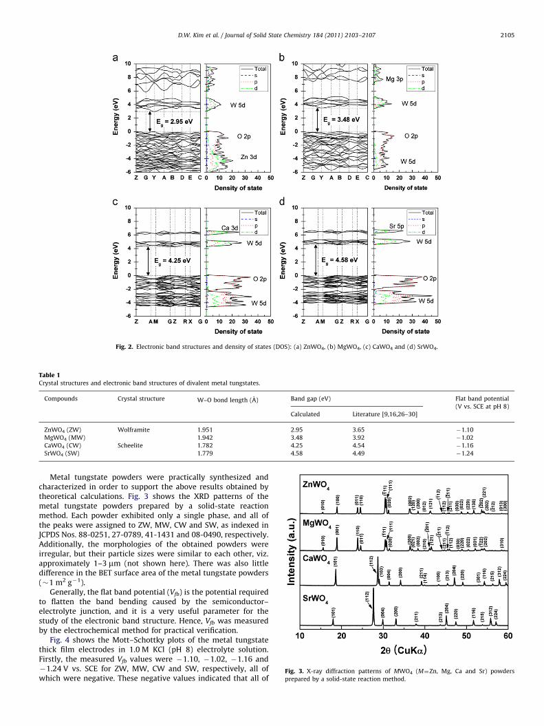
Fig. 2. Electronic band structures and density of states (DOS): (a) ZnWO4, (b) MgWO4, (c) CaWO4 and (d) SrWO4.
Table 1Crystal structures and electronic band structures of divalent metal tungstates.
Compounds Crystal structure W–O bond length (A) Band gap (eV) Flat band potential
(V vs. SCE at pH 8)
Calculated Literature [9,16,26–30]
ZnWO4 (ZW) Wolframite 1.951 2.95 3.65 �1.10
MgWO4 (MW) 1.942 3.48 3.92 �1.02
CaWO4 (CW) Scheelite 1.782 4.25 4.54 �1.16
SrWO4 (SW) 1.779 4.58 4.49 �1.24
Fig. 3. X-ray diffraction patterns of MWO4 (M¼Zn, Mg, Ca and Sr) powders
prepared by a solid-state reaction method.
D.W. Kim et al. / Journal of Solid State Chemistry 184 (2011) 2103–2107 2105
Metal tungstate powders were practically synthesized andcharacterized in order to support the above results obtained bytheoretical calculations. Fig. 3 shows the XRD patterns of themetal tungstate powders prepared by a solid-state reactionmethod. Each powder exhibited only a single phase, and all ofthe peaks were assigned to ZW, MW, CW and SW, as indexed inJCPDS Nos. 88-0251, 27-0789, 41-1431 and 08-0490, respectively.Additionally, the morphologies of the obtained powders wereirregular, but their particle sizes were similar to each other, viz.approximately 1–3 mm (not shown here). There was also littledifference in the BET surface area of the metal tungstate powders(�1 m2 g�1).
Generally, the flat band potential (Vfb) is the potential requiredto flatten the band bending caused by the semiconductor–electrolyte junction, and it is a very useful parameter for thestudy of the electronic band structure. Hence, Vfb was measuredby the electrochemical method for practical verification.
Fig. 4 shows the Mott–Schottky plots of the metal tungstatethick film electrodes in 1.0 M KCl (pH 8) electrolyte solution.Firstly, the measured Vfb values were �1.10, �1.02, �1.16 and�1.24 V vs. SCE for ZW, MW, CW and SW, respectively, all ofwhich were negative. These negative values indicated that all of
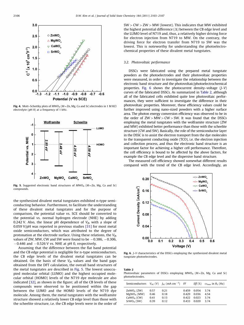
Fig. 4. Mott–Schottky plots of MWO4 (M¼Zn, Mg, Ca and Sr) electrodes in 1 M KCl
electrolyte (pH 8) at a frequency of 1 kHz.
Fig. 5. Suggested electronic band structures of MWO4 (M¼Zn, Mg, Ca and Sr)
compounds.
Fig. 6. J–V characteristics of the DSSCs employing the synthesized divalent metal
tungstate photoelectrodes.
Table 2Photovoltaic parameters of DSSCs employing MWO4 (M¼Zn, Mg, Ca and Sr)
photoelectrodes.
Semiconductors VOC (V) JSC (mA cm�2) FF Eff (%) omax in R3 (Hz)
ZnWO4 (ZW) 0.57 0.21 0.459 0.054 3.74
MgWO4 (MW) 0.46 0.18 0.429 0.036 4.54
CaWO4 (CW) 0.41 0.13 0.422 0.023 3.74
SrWO4 (SW) 0.39 0.12 0.433 0.020 3.74
D.W. Kim et al. / Journal of Solid State Chemistry 184 (2011) 2103–21072106
the synthesized divalent metal tungstates exhibited n-type semi-conducting behavior. Furthermore, to facilitate the understandingof these divalent metal tungstates and for the purpose ofcomparison, the potential value vs. SCE should be converted tothe potential vs. normal hydrogen electrode (NHE) by adding0.242 V. Also, the linear pH dependence of Vfb with a slope of0.059 V/pH was reported in previous studies [31] for most metaloxide semiconductors, which was attributed to the degree ofprotonation at the electrode surface. Using these relations, the Vfb
values of ZW, MW, CW and SW were found to be �0.386, �0.306,�0.446 and �0.526 V vs. NHE at pH 0, respectively.
Assuming that the difference between the flat band potentialand the CB edge potential is negligible for n-type semiconductors,the CB edge levels of the divalent metal tungstates can beobtained. On the basis of these Vfb values and the band gapsobtained from the DFT calculation, the overall band structures ofthe metal tungstates are described in Fig. 5. The lowest unoccu-pied molecular orbital (LUMO) and the highest occupied mole-cular orbital (HOMO) levels of the N719 dye molecule are alsoindicated [32], as shown in the figure; all of the CB levels of thesecompounds were observed to be positioned within the gapbetween the LUMO and the HOMO levels of the N719 dyemolecule. Among them, the metal tungstates with the wolframitestructure showed a relatively lower CB edge level than those withthe scheelite structure, i.e. the CB edge levels were in the order of
SW4CW4ZW4MW (lowest). This indicates that MW exhibitedthe highest potential difference (D) between the CB edge level andthe LUMO level of N719 and, thus, a relatively higher driving forcefor electron injection from N719 to MW. On the contrary, thedriving force for electron transfer from N719 to SW was thelowest. This is noteworthy for understanding the photoelectro-chemical properties of these divalent metal tungstates.
3.2. Photovoltaic performance
DSSCs were fabricated using the prepared metal tungstatepowders as the photoelectrodes and their photovoltaic propertieswere measured, in order to investigate the relationship between theelectronic band structure and the photovoltaic/photoelectrochemicalproperties. Fig. 6 shows the photocurrent density–voltage (J–V)curves of the fabricated DSSCs. As summarized in Table 2, althoughall of the fabricated cells exhibited quite low photovoltaic perfor-mances, they were sufficient to investigate the difference in theirphotovoltaic properties. Moreover, these efficiency values could befurther improved using nano-sized powders with a higher surfacearea. The photon energy conversion efficiency was observed to be inthe order of ZW4MW4CW4SW. It was found that the DSSCsemploying the metal tungstates with the wolframite structure (ZWand MW) exhibited better performance than those with the scheelitestructure (CW and SW). Basically, the role of the semiconductor layerin the DSSC is to assist the electron transport from the dye moleculesto the transparent conducting oxide (TCO), i.e. the electron injectionand collection process, and thus the electronic band structure is animportant factor for achieving a higher cell performance. Therefore,the cell efficiency is bound to be affected by the above factors, forexample the CB edge level and the dispersive band structure.
The measured cell efficiency showed somewhat different resultscompared with the trend of the CB edge level. Accordingly, an
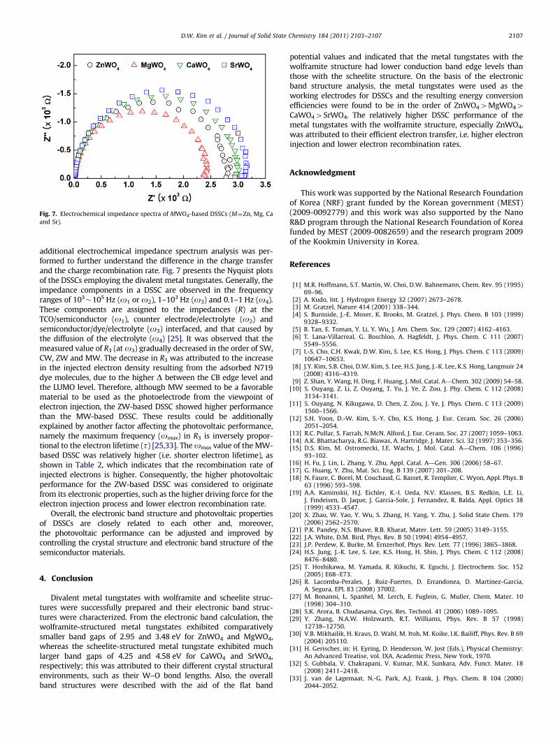
Fig. 7. Electrochemical impedance spectra of MWO4-based DSSCs (M¼Zn, Mg, Ca
and Sr).
D.W. Kim et al. / Journal of Solid State Chemistry 184 (2011) 2103–2107 2107
additional electrochemical impedance spectrum analysis was per-formed to further understand the difference in the charge transferand the charge recombination rate. Fig. 7 presents the Nyquist plotsof the DSSCs employing the divalent metal tungstates. Generally, theimpedance components in a DSSC are observed in the frequencyranges of 103
�105 Hz (o1 or o2), 1–103 Hz (o3) and 0.1–1 Hz (o4).These components are assigned to the impedances (R) at theTCO/semiconductor (o1), counter electrode/electrolyte (o2) andsemiconductor/dye/electrolyte (o3) interfaced, and that caused bythe diffusion of the electrolyte (o4) [25]. It was observed that themeasured value of R3 (at o3) gradually decreased in the order of SW,CW, ZW and MW. The decrease in R3 was attributed to the increasein the injected electron density resulting from the adsorbed N719dye molecules, due to the higher D between the CB edge level andthe LUMO level. Therefore, although MW seemed to be a favorablematerial to be used as the photoelectrode from the viewpoint ofelectron injection, the ZW-based DSSC showed higher performancethan the MW-based DSSC. These results could be additionallyexplained by another factor affecting the photovoltaic performance,namely the maximum frequency (omax) in R3 is inversely propor-tional to the electron lifetime (t) [25,33]. The omax value of the MW-based DSSC was relatively higher (i.e. shorter electron lifetime), asshown in Table 2, which indicates that the recombination rate ofinjected electrons is higher. Consequently, the higher photovoltaicperformance for the ZW-based DSSC was considered to originatefrom its electronic properties, such as the higher driving force for theelectron injection process and lower electron recombination rate.
Overall, the electronic band structure and photovoltaic propertiesof DSSCs are closely related to each other and, moreover,the photovoltaic performance can be adjusted and improved bycontrolling the crystal structure and electronic band structure of thesemiconductor materials.
4. Conclusion
Divalent metal tungstates with wolframite and scheelite struc-tures were successfully prepared and their electronic band struc-tures were characterized. From the electronic band calculation, thewolframite-structured metal tungstates exhibited comparativelysmaller band gaps of 2.95 and 3.48 eV for ZnWO4 and MgWO4,whereas the scheelite-structured metal tungstate exhibited muchlarger band gaps of 4.25 and 4.58 eV for CaWO4 and SrWO4,respectively; this was attributed to their different crystal structuralenvironments, such as their W–O bond lengths. Also, the overallband structures were described with the aid of the flat band
potential values and indicated that the metal tungstates with thewolframite structure had lower conduction band edge levels thanthose with the scheelite structure. On the basis of the electronicband structure analysis, the metal tungstates were used as theworking electrodes for DSSCs and the resulting energy conversionefficiencies were found to be in the order of ZnWO44MgWO44CaWO44SrWO4. The relatively higher DSSC performance of themetal tungstates with the wolframite structure, especially ZnWO4,was attributed to their efficient electron transfer, i.e. higher electroninjection and lower electron recombination rates.
Acknowledgment
This work was supported by the National Research Foundationof Korea (NRF) grant funded by the Korean government (MEST)(2009-0092779) and this work was also supported by the NanoR&D program through the National Research Foundation of Koreafunded by MEST (2009-0082659) and the research program 2009of the Kookmin University in Korea.
References
[1] M.R. Hoffmann, S.T. Martin, W. Choi, D.W. Bahnemann, Chem. Rev. 95 (1995)69–96.
[2] A. Kudo, Int. J. Hydrogen Energy 32 (2007) 2673–2678.[3] M. Gratzel, Nature 414 (2001) 338–344.[4] S. Burnside, J.-E. Moser, K. Brooks, M. Gratzel, J. Phys. Chem. B 103 (1999)
9328–9332.[5] B. Tan, E. Toman, Y. Li, Y. Wu, J. Am. Chem. Soc. 129 (2007) 4162–4163.[6] T. Lana-Villarreal, G. Boschloo, A. Hagfeldt, J. Phys. Chem. C 111 (2007)
5549–5556.[7] I.-S. Cho, C.H. Kwak, D.W. Kim, S. Lee, K.S. Hong, J. Phys. Chem. C 113 (2009)
10647–10653.[8] J.Y. Kim, S.B. Choi, D.W. Kim, S. Lee, H.S. Jung, J.-K. Lee, K.S. Hong, Langmuir 24
(2008) 4316–4319.[9] Z. Shan, Y. Wang, H. Ding, F. Huang, J. Mol. Catal. A—Chem. 302 (2009) 54–58.
[10] S. Ouyang, Z. Li, Z. Ouyang, T. Yu, J. Ye, Z. Zou, J. Phy. Chem. C 112 (2008)3134–3141.
[11] S. Ouyang, N. Kikugawa, D. Chen, Z. Zou, J. Ye, J. Phys. Chem. C 113 (2009)1560–1566.
[12] S.H. Yoon, D.-W. Kim, S.-Y. Cho, K.S. Hong, J. Eur. Ceram. Soc. 26 (2006)2051–2054.
[13] R.C. Pullar, S. Farrah, N.McN. Alford, J. Eur. Ceram. Soc. 27 (2007) 1059–1063.[14] A.K. Bhattacharya, R.G. Biawas, A. Hartridge, J. Mater. Sci. 32 (1997) 353–356.[15] D.S. Kim, M. Ostromecki, I.E. Wachs, J. Mol. Catal. A—Chem. 106 (1996)
93–102.[16] H. Fu, J. Lin, L. Zhang, Y. Zhu, Appl. Catal. A—Gen. 306 (2006) 58–67.[17] G. Huang, Y. Zhu, Mat. Sci. Eng. B 139 (2007) 201–208.[18] N. Faure, C. Borel, M. Couchaud, G. Basset, R. Templier, C. Wyon, Appl. Phys. B
63 (1996) 593–598.[19] A.A. Kaminskii, H.J. Eichler, K.-I. Ueda, N.V. Klassen, B.S. Redkin, L.E. Li,
J. Findeisen, D. Jaque, J. Garcia-Sole, J. Fernandez, R. Balda, Appl. Optics 38(1999) 4533–4547.
[20] X. Zhao, W. Yao, Y. Wu, S. Zhang, H. Yang, Y. Zhu, J. Solid State Chem. 179(2006) 2562–2570.
[21] P.K. Pandey, N.S. Bhave, R.B. Kharat, Mater. Lett. 59 (2005) 3149–3155.[22] J.A. White, D.M. Bird, Phys. Rev. B 50 (1994) 4954–4957.[23] J.P. Perdew, K. Burke, M. Ernzerhof, Phys. Rev. Lett. 77 (1996) 3865–3868.[24] H.S. Jung, J.-K. Lee, S. Lee, K.S. Hong, H. Shin, J. Phys. Chem. C 112 (2008)
8476–8480.[25] T. Hoshikawa, M. Yamada, R. Kikuchi, K. Eguchi, J. Electrochem. Soc. 152
(2005) E68–E73.[26] R. Lacomba-Perales, J. Ruiz-Fuertes, D. Errandonea, D. Martinez-Garcia,
A. Segura, EPL 83 (2008) 37002.[27] M. Bonanni, L. Spanhel, M. Lerch, E. Fuglein, G. Muller, Chem. Mater. 10
(1998) 304–310.[28] S.K. Arora, B. Chudasama, Crys. Res. Technol. 41 (2006) 1089–1095.[29] Y. Zhang, N.A.W. Holzwarth, R.T. Williams, Phys. Rev. B 57 (1998)
12738–12750.[30] V.B. Mikhailik, H. Kraus, D. Wahl, M. Itoh, M. Koike, I.K. Bailiff, Phys. Rev. B 69
(2004) 205110.[31] H. Gerischer, in: H. Eyring, D. Henderson, W. Jost (Eds.), Physical Chemistry:
An Advanced Treatise, vol. IXA, Academic Press, New York, 1970.[32] S. Gubbala, V. Chakrapani, V. Kumar, M.K. Sunkara, Adv. Funct. Mater. 18
(2008) 2411–2418.[33] J. van de Lagemaat, N.-G. Park, A.J. Frank, J. Phys. Chem. B 104 (2000)
2044–2052.