electronic circuits electrical etc, connected together in...
TRANSCRIPT

Electronic Circuits
Dr. Edmund Lam
Department of Electrical and Electronic EngineeringThe University of Hong Kong
ENGG1203: Introduction to Electrical and Electronic Engineering(Second Semester, 2017–18)
http://www.eee.hku.hk/˜engg1203
E. Lam (University of Hong Kong) ENGG1203 March, 2018 1 / 80
Introduction
Electrical/electronic circuits consist of voltage sources, resistors, wires,etc, connected together in a closed path.
In logic circuits, inputs and outputs are Boolean values: either0 (LOW) or 1 (HIGH).In (analog) electrical/electronic circuits, quantities — voltages andcurrents — take on values within a continuous range.We interface the two using analog-to-digital conversion (ADC)and digital-to-analog conversion (DAC).
Note: We can also understand electronic circuits to be at a lower abstraction level than logiccircuits; if we ask how a logic gate is built, we will see that it is by using electronic componentswe are going to study here. We will come back to this viewpoint later on.
E. Lam (University of Hong Kong) ENGG1203 March, 2018 2 / 80
Big picture of engineering analysis
1 Big picture of engineering analysis
2 Building and analysis of electrical/electronic circuits
3 Circuit theorems: superposition, Thevenin, Norton
4 Interface with (digital) logic circuits
5 Buffers and op-amps
6 Integrated circuits
E. Lam (University of Hong Kong) ENGG1203 March, 2018 3 / 80
Big picture of engineering analysis
Big Picture of Engineering Analysis
+− R1
R2 R3
+− Req
Req = R1 + (R−12 + R−1
3 )−1
model
analysis using rules
experiment
E. Lam (University of Hong Kong) ENGG1203 March, 2018 4 / 80

Big picture of engineering analysis
Big Picture of Engineering Analysis
Model:In ENGG1203, models are mostly given to youIn the future, as you know more engineering, you will haveopportunities to develop models yourselves
Rules:Lectures, tutorials, homework, final are mostly about teaching youthe rules
Experiment:Labs are mostly about experiments
E. Lam (University of Hong Kong) ENGG1203 March, 2018 5 / 80
Big picture of engineering analysis
Big Picture of Engineering Analysis
Model:In ENGG1203, we will mostly be modeling electrical components:
Understanding biological cells and brain functions:system biology and computational neurosciencehttp://lifesciences.ieee.org/
Other system that has the same mathematical properties
E. Lam (University of Hong Kong) ENGG1203 March, 2018 6 / 80
Big picture of engineering analysis
Big Picture of Engineering Analysis
Rules:Rules are governed by mathematicsThere are “theorems” or “laws”
Same is true for digital logic:1 + 1 = 10 · 1 = 0a · b = a + b (De Morgan’s theorem)
E. Lam (University of Hong Kong) ENGG1203 March, 2018 7 / 80
Building and analysis of electrical/electronic circuits
1 Big picture of engineering analysis
2 Building and analysis of electrical/electronic circuits
3 Circuit theorems: superposition, Thevenin, Norton
4 Interface with (digital) logic circuits
5 Buffers and op-amps
6 Integrated circuits
E. Lam (University of Hong Kong) ENGG1203 March, 2018 8 / 80

Building and analysis of electrical/electronic circuits
Electrical Circuit
Goal: To be able to build and analyze electrical circuits
What are the electrical circuit components?What are their models?What are the rules?How do we do the analyses?What conclusions can we make?
E. Lam (University of Hong Kong) ENGG1203 March, 2018 9 / 80
Building and analysis of electrical/electronic circuits
Components
(Ideal) voltage source
+−
+v−
or+v−
Rules:Supply constant voltage v across the two terminals, and there is noconstraint on the currentReality: battery voltage can drop after prolonged use, current cannot betoo big, etc — we will ignore these in our model!
E. Lam (University of Hong Kong) ENGG1203 March, 2018 10 / 80
Building and analysis of electrical/electronic circuits
Components
(Ideal) current source
i
Rules:Supply constant current i from the positive terminal, irrespectiveof voltage levelReality: Similar to the ideal voltage source, nothing can supply aconstant irrespective of other components in the circuit
E. Lam (University of Hong Kong) ENGG1203 March, 2018 11 / 80
Building and analysis of electrical/electronic circuits
Components
Resistor
R
I+
V−
V = voltage across the resistor
I = current through the resistor
Rules:
Ohm’s law: V = IR
Reality: linear relationship holds only for a limited range of V and I —we will ignore this in our model!
E. Lam (University of Hong Kong) ENGG1203 March, 2018 12 / 80
Building and analysis of electrical/electronic circuits
Components
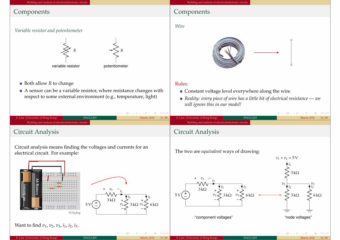
Variable resistor and potentiometer
R
variable resistor
R
potentiometer
Both allow R to changeA sensor can be a variable resistor, where resistance changes withrespect to some external environment (e.g., temperature, light)
E. Lam (University of Hong Kong) ENGG1203 March, 2018 13 / 80
Building and analysis of electrical/electronic circuits
Components
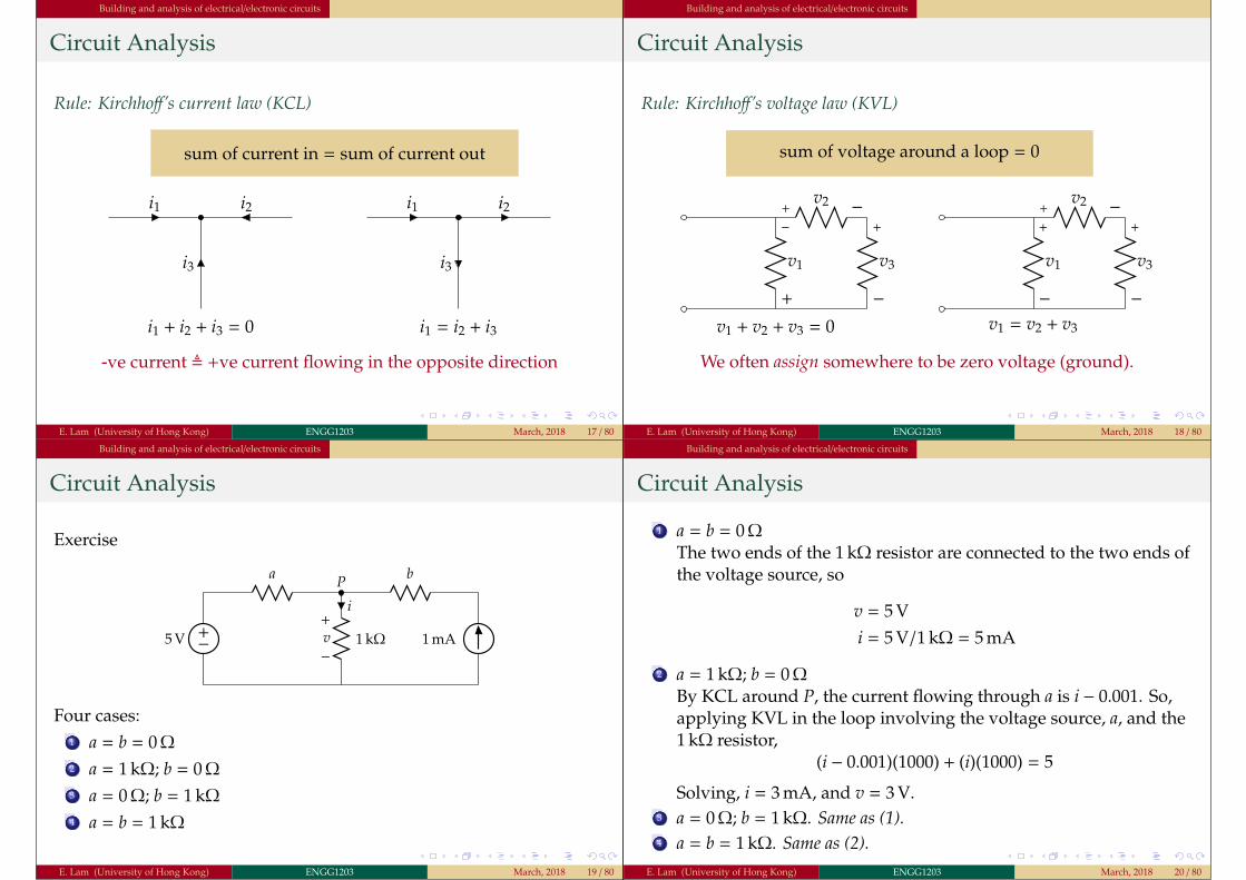
Wire
Rules:Constant voltage level everywhere along the wireReality: every piece of wire has a little bit of electrical resistance — wewill ignore this in our model!
E. Lam (University of Hong Kong) ENGG1203 March, 2018 14 / 80
Building and analysis of electrical/electronic circuits
Circuit Analysis
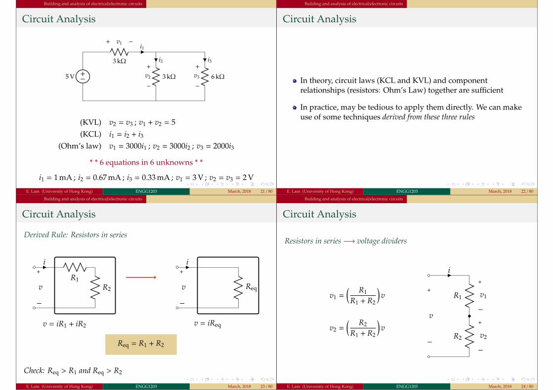
Circuit analysis means finding the voltages and currents for anelectrical circuit. For example:
+−5 V3 kΩ
i1+ v1 −
3 kΩ
i2+v2−
6 kΩ
i3+v3−
Want to find v1, v2, v3, i1, i2, i3.
E. Lam (University of Hong Kong) ENGG1203 March, 2018 15 / 80
Building and analysis of electrical/electronic circuits
Circuit Analysis
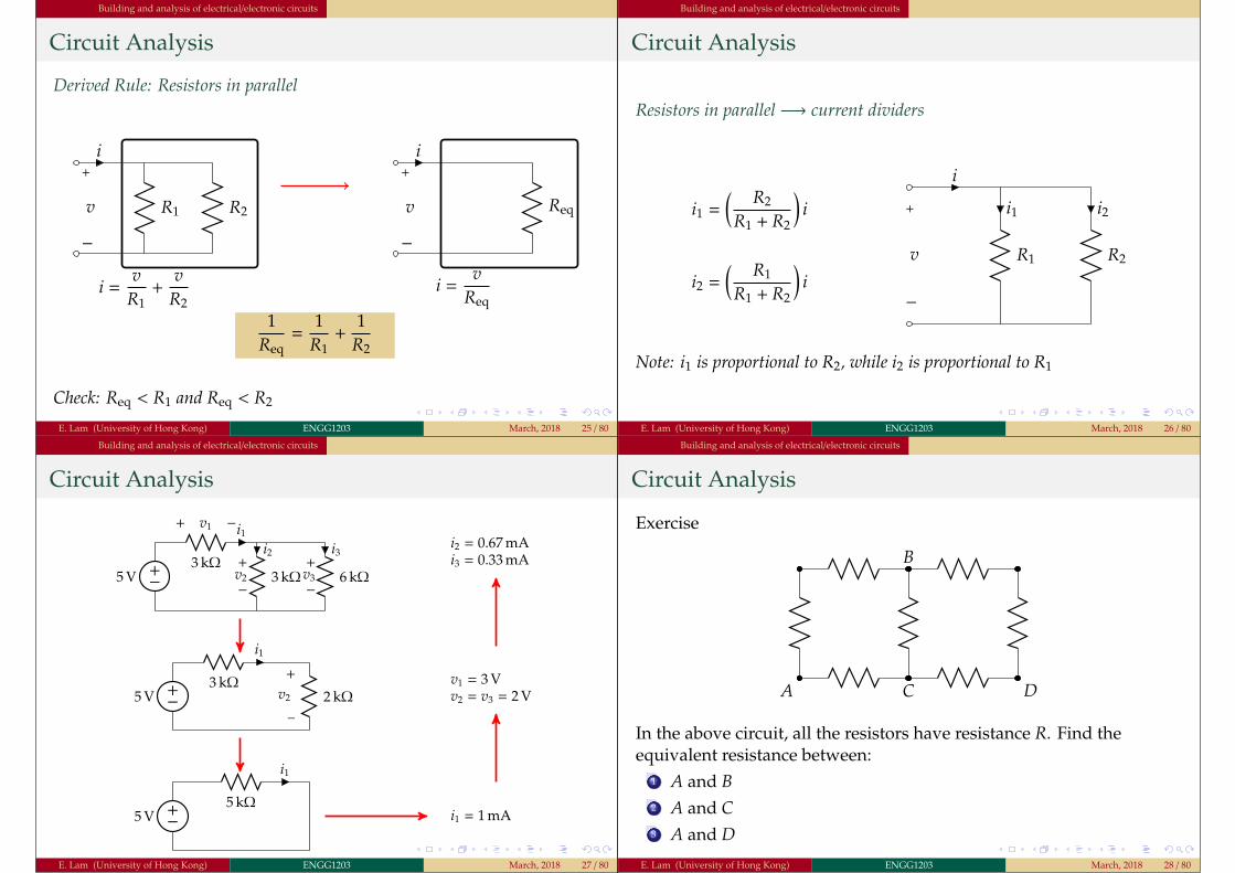
The two are equivalent ways of drawing:
+−5 V3 kΩ
i1+ v1 −
3 kΩ
i2+v2
−6 kΩ
i3+v3
−
“component voltages”
v1 + v2 = 5 V
3 kΩ
i1
v2
3 kΩ
i2v3
6 kΩ
i3
“node voltages”
E. Lam (University of Hong Kong) ENGG1203 March, 2018 16 / 80
Building and analysis of electrical/electronic circuits
Circuit Analysis
Rule: Kirchhoff’s current law (KCL)
sum of current in = sum of current out
i1 i2
i3
i1 + i2 + i3 = 0
i1 i2
i3
i1 = i2 + i3
-ve current , +ve current flowing in the opposite direction
E. Lam (University of Hong Kong) ENGG1203 March, 2018 17 / 80
Building and analysis of electrical/electronic circuits
Circuit Analysis
Rule: Kirchhoff’s voltage law (KVL)
sum of voltage around a loop = 0
+ −v2
+
−v3
−
+
v1
v1 + v2 + v3 = 0
+ −v2
+
−v3
+
−v1
v1 = v2 + v3
We often assign somewhere to be zero voltage (ground).
E. Lam (University of Hong Kong) ENGG1203 March, 2018 18 / 80
Building and analysis of electrical/electronic circuits
Circuit Analysis
Exercise
+−5 V
a P b
1 kΩ
i+v−
1 mA
Four cases:1 a = b = 0 Ω
2 a = 1 kΩ; b = 0 Ω
3 a = 0 Ω; b = 1 kΩ
4 a = b = 1 kΩ
E. Lam (University of Hong Kong) ENGG1203 March, 2018 19 / 80
Building and analysis of electrical/electronic circuits
Circuit Analysis
1 a = b = 0 ΩThe two ends of the 1 kΩ resistor are connected to the two ends ofthe voltage source, so
v = 5 Vi = 5 V/1 kΩ = 5 mA
2 a = 1 kΩ; b = 0 ΩBy KCL around P, the current flowing through a is i − 0.001. So,applying KVL in the loop involving the voltage source, a, and the1 kΩ resistor,
(i − 0.001)(1000) + (i)(1000) = 5
Solving, i = 3 mA, and v = 3 V.3 a = 0 Ω; b = 1 kΩ. Same as (1).4 a = b = 1 kΩ. Same as (2).
E. Lam (University of Hong Kong) ENGG1203 March, 2018 20 / 80
Building and analysis of electrical/electronic circuits
Circuit Analysis
+−5 V
3 kΩ
i1+ v1 −
3 kΩ
i2+
v2
−6 kΩ
i3+
v3
−
(KVL) v2 = v3 ; v1 + v2 = 5(KCL) i1 = i2 + i3
(Ohm’s law) v1 = 3000i1 ; v2 = 3000i2 ; v3 = 2000i3
* * 6 equations in 6 unknowns * *
i1 = 1 mA ; i2 = 0.67 mA ; i3 = 0.33 mA ; v1 = 3 V ; v2 = v3 = 2 V
E. Lam (University of Hong Kong) ENGG1203 March, 2018 21 / 80
Building and analysis of electrical/electronic circuits
Circuit Analysis
In theory, circuit laws (KCL and KVL) and componentrelationships (resistors: Ohm’s Law) together are sufficient
In practice, may be tedious to apply them directly. We can makeuse of some techniques derived from these three rules
E. Lam (University of Hong Kong) ENGG1203 March, 2018 22 / 80
Building and analysis of electrical/electronic circuits
Circuit Analysis
Derived Rule: Resistors in series
i
R1R2
+
−v
v = iR1 + iR2
Req = R1 + R2
i
Req
+
−v
v = iReq
Check: Req > R1 and Req > R2
E. Lam (University of Hong Kong) ENGG1203 March, 2018 23 / 80
Building and analysis of electrical/electronic circuits
Circuit Analysis
Resistors in series −→ voltage dividers
i
R1
R2
+
−v1
+
−v2
+
−
v
v1 =( R1
R1 + R2
)v
v2 =( R2
R1 + R2
)v
E. Lam (University of Hong Kong) ENGG1203 March, 2018 24 / 80
Building and analysis of electrical/electronic circuits
Circuit Analysis
Derived Rule: Resistors in parallel
i
R1 R2
+
−v
i =v
R1+
vR2
1Req
=1
R1+
1R2
i
Req
+
−v
i =v
Req
Check: Req < R1 and Req < R2
E. Lam (University of Hong Kong) ENGG1203 March, 2018 25 / 80
Building and analysis of electrical/electronic circuits
Circuit Analysis
Resistors in parallel −→ current dividers
i
R1
i1
R2
i2+
−
v
i1 =( R2
R1 + R2
)i
i2 =( R1
R1 + R2
)i
Note: i1 is proportional to R2, while i2 is proportional to R1
E. Lam (University of Hong Kong) ENGG1203 March, 2018 26 / 80
Building and analysis of electrical/electronic circuits
Circuit Analysis
+−5 V3 kΩ
i1+ v1 −
3 kΩ
i2+v2− 6 kΩ
i3+v3−
+−5 V3 kΩ
i1
2 kΩ
−
+
v2
+−5 V5 kΩ
i1
i1 = 1 mA
v1 = 3 Vv2 = v3 = 2 V
i2 = 0.67 mAi3 = 0.33 mA
E. Lam (University of Hong Kong) ENGG1203 March, 2018 27 / 80
Building and analysis of electrical/electronic circuits
Circuit Analysis
Exercise
B
DCA
In the above circuit, all the resistors have resistance R. Find theequivalent resistance between:
1 A and B2 A and C3 A and D
E. Lam (University of Hong Kong) ENGG1203 March, 2018 28 / 80
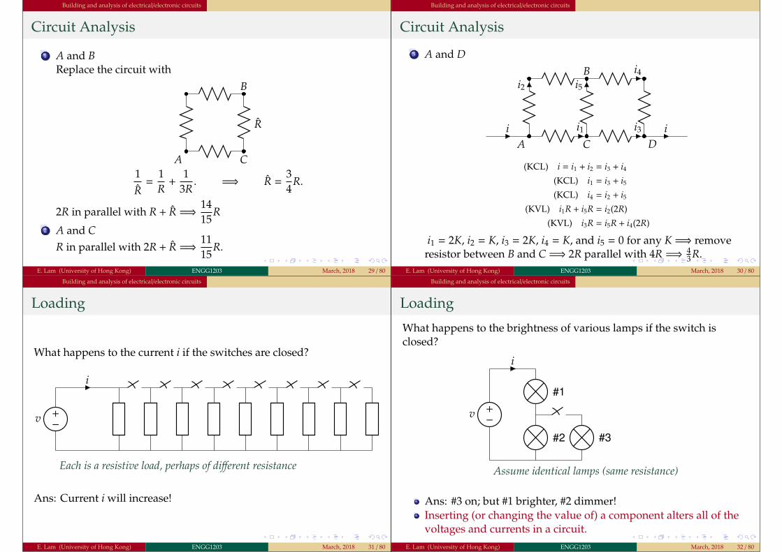
Building and analysis of electrical/electronic circuits
Circuit Analysis
1 A and BReplace the circuit with
B
R
CA1R
=1R
+1
3R. =⇒ R =
34
R.
2R in parallel with R + R =⇒ 1415
R2 A and C
R in parallel with 2R + R =⇒ 1115
R.
E. Lam (University of Hong Kong) ENGG1203 March, 2018 29 / 80
Building and analysis of electrical/electronic circuits
Circuit Analysis
3 A and D
iA
ii1C
i2 i5B
i3D
i4
(KCL) i = i1 + i2 = i3 + i4
(KCL) i1 = i3 + i5
(KCL) i4 = i2 + i5
(KVL) i1R + i5R = i2(2R)
(KVL) i3R = i5R + i4(2R)
i1 = 2K, i2 = K, i3 = 2K, i4 = K, and i5 = 0 for any K =⇒ removeresistor between B and C =⇒ 2R parallel with 4R =⇒ 4
3 R.E. Lam (University of Hong Kong) ENGG1203 March, 2018 30 / 80
Building and analysis of electrical/electronic circuits
Loading
What happens to the current i if the switches are closed?
+−v
i
Each is a resistive load, perhaps of different resistance
Ans: Current i will increase!
E. Lam (University of Hong Kong) ENGG1203 March, 2018 31 / 80
Building and analysis of electrical/electronic circuits
Loading
What happens to the brightness of various lamps if the switch isclosed?
+−v
i
#1
#2 #3
Assume identical lamps (same resistance)
Ans: #3 on; but #1 brighter, #2 dimmer!Inserting (or changing the value of) a component alters all of thevoltages and currents in a circuit.
E. Lam (University of Hong Kong) ENGG1203 March, 2018 32 / 80
Building and analysis of electrical/electronic circuits
Buffer
Want an ideal buffer to eliminate (or diminish) loading effect1 senses the voltage at its input without drawing any current2 sets its output voltage equal to the measured input voltage
+−v
i
#1
#2
iinbuffer
#3+
−vin
+
−vout
iin = 0, vout = vin
Will see how to approximate it with an op-amp later onE. Lam (University of Hong Kong) ENGG1203 March, 2018 33 / 80
Building and analysis of electrical/electronic circuits
Power and Energy
An important metric for an electrical circuit: power (energy)Power is the rate (per unit time) of delivering or absorbing energy
Mathematically, the product of voltage and current: P = v · iUnit: 1 W(watt) = 1 V(volt) × 1 A(ampere)
For resistors, P = i2R = v2/R
Note the direction of v versus i
i
−
+
v
current enters throughpositive terminal
=⇒ P = vi=⇒ absorbs power
i
−
+
v
current exits throughpositive terminal
=⇒ P = vi=⇒ delivers power
E. Lam (University of Hong Kong) ENGG1203 March, 2018 34 / 80
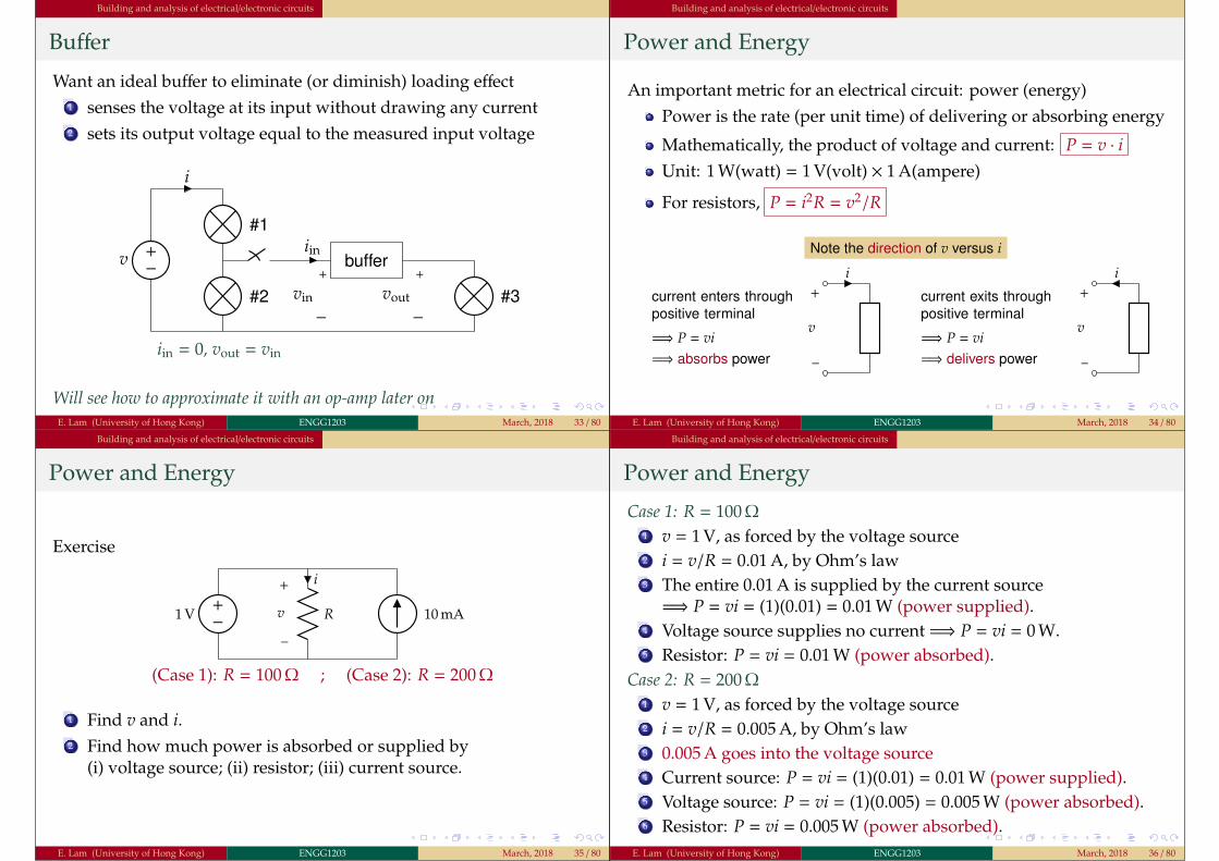
Building and analysis of electrical/electronic circuits
Power and Energy
Exercise
+−1 V R
i
10 mA
−
+
v
(Case 1): R = 100 Ω ; (Case 2): R = 200 Ω
1 Find v and i.2 Find how much power is absorbed or supplied by
(i) voltage source; (ii) resistor; (iii) current source.
E. Lam (University of Hong Kong) ENGG1203 March, 2018 35 / 80
Building and analysis of electrical/electronic circuits
Power and Energy
Case 1: R = 100 Ω
1 v = 1 V, as forced by the voltage source2 i = v/R = 0.01 A, by Ohm’s law3 The entire 0.01 A is supplied by the current source
=⇒ P = vi = (1)(0.01) = 0.01 W (power supplied).4 Voltage source supplies no current =⇒ P = vi = 0 W.5 Resistor: P = vi = 0.01 W (power absorbed).
Case 2: R = 200 Ω
1 v = 1 V, as forced by the voltage source2 i = v/R = 0.005 A, by Ohm’s law3 0.005 A goes into the voltage source4 Current source: P = vi = (1)(0.01) = 0.01 W (power supplied).5 Voltage source: P = vi = (1)(0.005) = 0.005 W (power absorbed).6 Resistor: P = vi = 0.005 W (power absorbed).
E. Lam (University of Hong Kong) ENGG1203 March, 2018 36 / 80
Circuit theorems: superposition, Thevenin, Norton
1 Big picture of engineering analysis
2 Building and analysis of electrical/electronic circuits
3 Circuit theorems: superposition, Thevenin, Norton
4 Interface with (digital) logic circuits
5 Buffers and op-amps
6 Integrated circuits
E. Lam (University of Hong Kong) ENGG1203 March, 2018 37 / 80
Circuit theorems: superposition, Thevenin, Norton
Superposition
Objective: decompose a circuit with multiple input sources intomultiple circuits with only 1 source
Superposition theorem: the response of a circuit with multiple inputsources is the sum of the responses from each independent source whenacting alone.To obtain the response due to one particular source, one wouldturn off all the other sources (voltage sources or current sources) inthe circuit except this one.Turning off a source can be achieved by the following rules:
For voltage sources, replace the source with a short circuit.For current sources, replace the source with an open circuit.
The overall response of the circuit can then be obtained bysuperpositioning (i.e., adding) each independent response on top ofeach other.
E. Lam (University of Hong Kong) ENGG1203 March, 2018 38 / 80
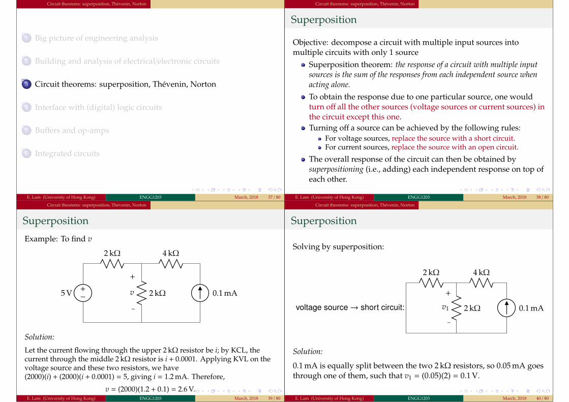
Circuit theorems: superposition, Thevenin, Norton
Superposition
Example: To find v
+−5 V
2 kΩ
2 kΩ 0.1 mA
4 kΩ
−
+
v
Solution:
Let the current flowing through the upper 2 kΩ resistor be i; by KCL, thecurrent through the middle 2 kΩ resistor is i + 0.0001. Applying KVL on thevoltage source and these two resistors, we have(2000)(i) + (2000)(i + 0.0001) = 5, giving i = 1.2 mA. Therefore,
v = (2000)(1.2 + 0.1) = 2.6 V.E. Lam (University of Hong Kong) ENGG1203 March, 2018 39 / 80
Circuit theorems: superposition, Thevenin, Norton
Superposition
Solving by superposition:
2 kΩ
2 kΩ 0.1 mA
4 kΩ
−
+
v1voltage source→ short circuit:
Solution:
0.1 mA is equally split between the two 2 kΩ resistors, so 0.05 mA goesthrough one of them, such that v1 = (0.05)(2) = 0.1 V.
E. Lam (University of Hong Kong) ENGG1203 March, 2018 40 / 80

Circuit theorems: superposition, Thevenin, Norton
Superposition
Solving by superposition:
+−5 V
2 kΩ
2 kΩ
4 kΩ
−
+
v2current source→ open circuit:
Solution:
5 V is equally divided between the two 2 kΩ resistors, so v2 = 2.5 V.
Therefore,v = 0.1 + 2.5 = 2.6 V.
E. Lam (University of Hong Kong) ENGG1203 March, 2018 41 / 80
Circuit theorems: superposition, Thevenin, Norton
Thevenin’s Theorem
Converts any complex circuits with voltage sources, current sources,and resistors into one — from the point of view of a load — with only asingle voltage source in series with a resistor:
B
+− vth
Rth
A
RL
iL+
−vL
B
A
RL
iL+
−vL
network of sourcesand resistors
RL is the load resistor connected to the terminals A and B.The Thevenin equivalent voltage, vth, is equal to the voltage acrossAB if there is no load, i.e., an open circuit;Calculate the current I when AB is short-ciruited. Then, theThevenin equivalent resistance, Rth, is equal to vth/I.
E. Lam (University of Hong Kong) ENGG1203 March, 2018 42 / 80
Circuit theorems: superposition, Thevenin, Norton
Thevenin’s Theorem
Example: Find the Thevenin equivalent voltage and resistance, andthen the resultant voltage across AB if they are connected by a 2 kΩresistor.
+− 5 V
2 kΩ
0.1 mA
4 kΩ
B
A
E. Lam (University of Hong Kong) ENGG1203 March, 2018 43 / 80
Circuit theorems: superposition, Thevenin, Norton
Thevenin’s TheoremAB is open circuit: The 0.1 mA from the current source can only go throughthe two resistors. Across the 2 kΩ resistor, it creates a voltage difference of0.2 V, adding to the 5 V source, vth = 5 + 0.2 = 5.2 V.AB is short circuit: 5 V must drop across the 2 kΩ resistor, so there is a currentof 2.5 mA. This is added to the 0.1 mA supplied by the current source, givingI = 2.6 mA. Therefore, Rth = 5.2/2.6 = 2 kΩ.
B
+− 5.2 V
2 kΩ
A
RL
iL+
−vL
When the load is a 2 kΩ resistor, half of the voltage drops across it,
vL = 5.2/2 = 2.6 V.
E. Lam (University of Hong Kong) ENGG1203 March, 2018 44 / 80
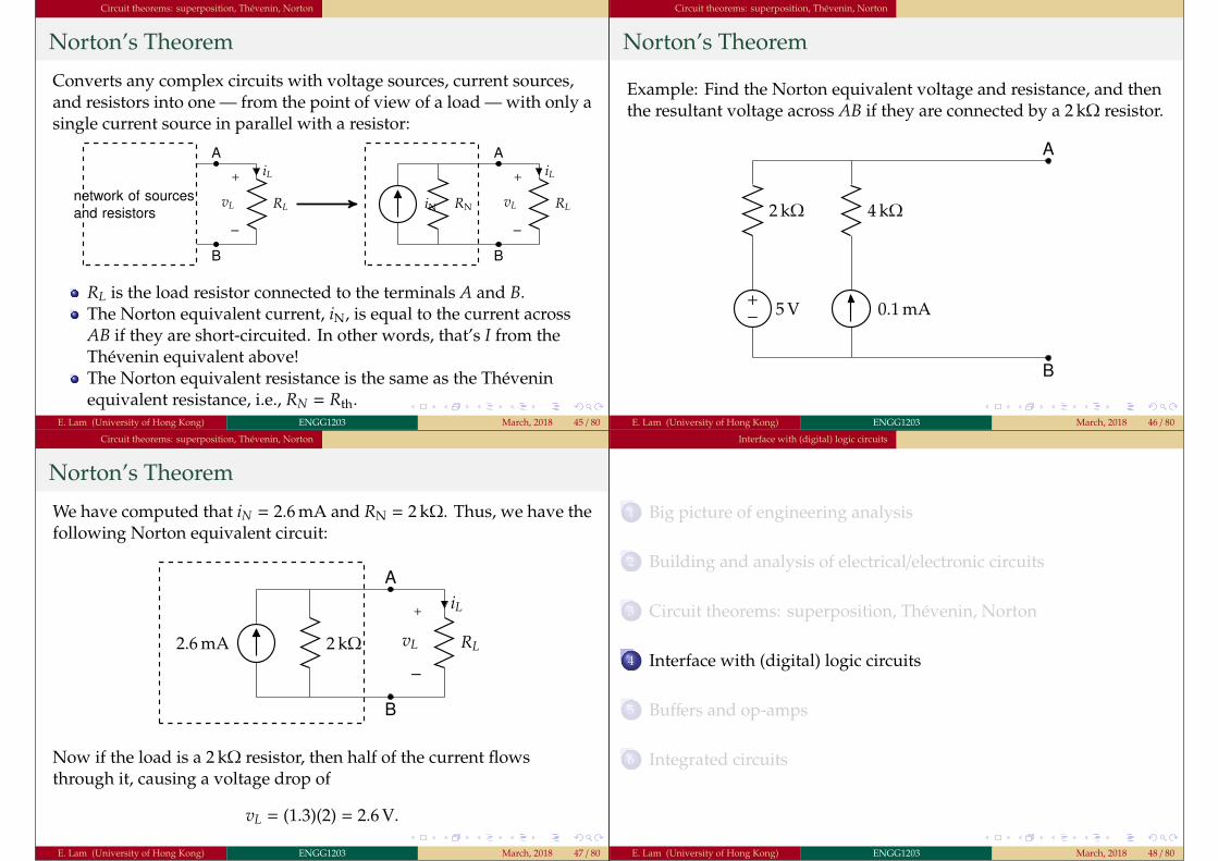
Circuit theorems: superposition, Thevenin, Norton
Norton’s Theorem
Converts any complex circuits with voltage sources, current sources,and resistors into one — from the point of view of a load — with only asingle current source in parallel with a resistor:
B
iN RN
A
RL
iL+
−vL
B
A
RL
iL+
−vL
network of sourcesand resistors
RL is the load resistor connected to the terminals A and B.The Norton equivalent current, iN, is equal to the current acrossAB if they are short-circuited. In other words, that’s I from theThevenin equivalent above!The Norton equivalent resistance is the same as the Theveninequivalent resistance, i.e., RN = Rth.
E. Lam (University of Hong Kong) ENGG1203 March, 2018 45 / 80
Circuit theorems: superposition, Thevenin, Norton
Norton’s Theorem
Example: Find the Norton equivalent voltage and resistance, and thenthe resultant voltage across AB if they are connected by a 2 kΩ resistor.
+− 5 V
2 kΩ
0.1 mA
4 kΩ
B
A
E. Lam (University of Hong Kong) ENGG1203 March, 2018 46 / 80
Circuit theorems: superposition, Thevenin, Norton
Norton’s Theorem
We have computed that iN = 2.6 mA and RN = 2 kΩ. Thus, we have thefollowing Norton equivalent circuit:
B
2.6 mA 2 kΩ
A
RL
iL+
−vL
Now if the load is a 2 kΩ resistor, then half of the current flowsthrough it, causing a voltage drop of
vL = (1.3)(2) = 2.6 V.
E. Lam (University of Hong Kong) ENGG1203 March, 2018 47 / 80
Interface with (digital) logic circuits
1 Big picture of engineering analysis
2 Building and analysis of electrical/electronic circuits
3 Circuit theorems: superposition, Thevenin, Norton
4 Interface with (digital) logic circuits
5 Buffers and op-amps
6 Integrated circuits
E. Lam (University of Hong Kong) ENGG1203 March, 2018 48 / 80

Interface with (digital) logic circuits
Motivation
Consider this problem: We want to turn on a warning light if thesurrounding temperature is too high
1 Need to sense the temperatureUse a thermistor modeled as a variable resistorAssume resistance decreases as temperature increases
2 Need to process the inputAssume this is done digitally
3 Need to output something to turn on the lightAssume this is done by adjusting the voltage
E. Lam (University of Hong Kong) ENGG1203 March, 2018 49 / 80
Interface with (digital) logic circuits
Design model
Use the following high-level design model
input process outputtemperature light
analog digital digital analog
Need ADC:voltage→ digital value
Need DAC:digital value→ voltage
E. Lam (University of Hong Kong) ENGG1203 March, 2018 50 / 80
Interface with (digital) logic circuits
ADC
(One-bit) analog-to-digital converter (ADC):
ADCinput analog voltage output logic value: 0 or 1
physically still a (fixed) voltage
ADC performs thresholding: for a pre-defined threshold vt,if input voltage v ≥ vt, then output 1if input voltage v < vt, then output 0
Can think of it as making a binary decision on the inputOutput physically may be, e.g., 0 V vs 12 V, or 0 V vs 3.3 V, or anypair of pre-defined values
E. Lam (University of Hong Kong) ENGG1203 March, 2018 51 / 80
Interface with (digital) logic circuits
Input Design
An example design of the input:
vcc
Rref
vout
Rt
ADC a
temperature→ Rt → vout → a
vout =Rt
Rref + Rtvcc
a = 1 if vout ≥ vt
a = 0 if vout < vt
high temperature→ Rt ↓→ vout ≈ 0→ a = 0low temperature→ Rt ↑→ vout ≈ vcc → a = 1
E. Lam (University of Hong Kong) ENGG1203 March, 2018 52 / 80

Interface with (digital) logic circuits
Input Design
An example design of the input:
vcc
Rref
vout
Rt
ADC a
assume such thermistor:
hot coldRt = Rref/3 Rt = Rref
Vout = 14 vcc Vout = 1
2 vcc
set vt =38
vcc
E. Lam (University of Hong Kong) ENGG1203 March, 2018 53 / 80
Interface with (digital) logic circuits
Process Design
In this example design, high temperature gives 0 and low temperaturegives 1, but we want high temperature to trigger the light
process = a NOT gate
In general, the process can be (very complicated) digital logic!
E. Lam (University of Hong Kong) ENGG1203 March, 2018 54 / 80
Interface with (digital) logic circuits
Output Design
An example design of the output:
a DAC
temperature→ Rt → vout → a
a→ a
a→ light
E. Lam (University of Hong Kong) ENGG1203 March, 2018 55 / 80
Interface with (digital) logic circuits
DAC
(One-bit) digital-to-analog converter (DAC):
DACinput logic value: 0 or 1 output analog voltage
physically still a (fixed) voltage
Output (analog) voltage is not necessarily equal to the inputvoltage underlying the logic valuesLogical values 0 and 1 should not be used to drive output directly
E. Lam (University of Hong Kong) ENGG1203 March, 2018 56 / 80
Interface with (digital) logic circuits
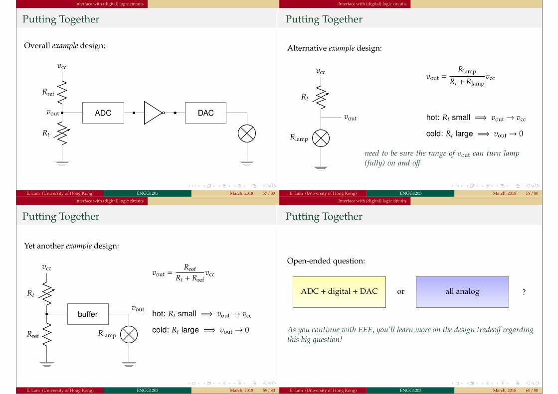
Putting Together
Overall example design:
vcc
Rref
vout
Rt
ADC DAC
E. Lam (University of Hong Kong) ENGG1203 March, 2018 57 / 80
Interface with (digital) logic circuits
Putting Together
Alternative example design:
vcc
Rt
Rlamp
vout
vout =Rlamp
Rt + Rlampvcc
hot: Rt small =⇒ vout → vcc
cold: Rt large =⇒ vout → 0
need to be sure the range of vout can turn lamp(fully) on and off
E. Lam (University of Hong Kong) ENGG1203 March, 2018 58 / 80
Interface with (digital) logic circuits
Putting Together
Yet another example design:
vcc
Rt
Rref
buffervout
Rlamp
vout =Rref
Rt + Rrefvcc
hot: Rt small =⇒ vout → vcc
cold: Rt large =⇒ vout → 0
E. Lam (University of Hong Kong) ENGG1203 March, 2018 59 / 80
Interface with (digital) logic circuits
Putting Together
Open-ended question:
ADC + digital + DAC or all analog ?
As you continue with EEE, you’ll learn more on the design tradeoff regardingthis big question!
E. Lam (University of Hong Kong) ENGG1203 March, 2018 60 / 80
Buffers and op-amps
1 Big picture of engineering analysis
2 Building and analysis of electrical/electronic circuits
3 Circuit theorems: superposition, Thevenin, Norton
4 Interface with (digital) logic circuits
5 Buffers and op-amps
6 Integrated circuits
E. Lam (University of Hong Kong) ENGG1203 March, 2018 61 / 80
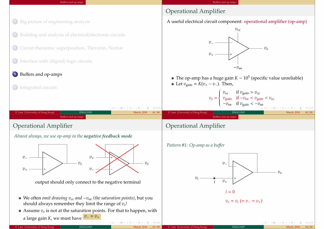
Buffers and op-amps
Operational Amplifier
A useful electrical circuit component: operational amplifier (op-amp)
−
+
v−
v+
vo
vcc
−vee
The op-amp has a huge gain K ∼ 105 (specific value unreliable)Let vgain = K(v+ − v−). Then,
vo =
vcc if vgain > vccvgain if −vee < vgain < vcc−vee if vgain < −vee
E. Lam (University of Hong Kong) ENGG1203 March, 2018 62 / 80
Buffers and op-amps
Operational Amplifier
Almost always, we use op-amp in the negative feedback mode
−
+
v−
v+
vo−
+
v−
v+
vo
output should only connect to the negative terminal
We often omit drawing vcc and −vee (the saturation points), but youshould always remember they limit the range of vo!Assume vo is not at the saturation points. For that to happen, with
a large gain K, we must have v− ≈ v+
E. Lam (University of Hong Kong) ENGG1203 March, 2018 63 / 80
Buffers and op-amps
Operational Amplifier
Pattern #1: Op-amp as a buffer
−
+
v−
v+ivi
vo
i = 0
vo = vi (= v− = v+)
E. Lam (University of Hong Kong) ENGG1203 March, 2018 64 / 80
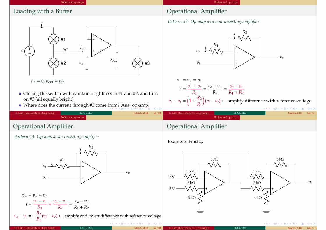
Buffers and op-amps
Loading with a Buffer
−
+
+−v
i
#1
#2
iin
#3+
−vin
+
−vout
iin = 0, vout = vin
Closing the switch will maintain brightness in #1 and #2, and turnon #3 (all equally bright)Where does the current through #3 come from? Ans: op-amp!
E. Lam (University of Hong Kong) ENGG1203 March, 2018 65 / 80
Buffers and op-amps
Operational Amplifier
Pattern #2: Op-amp as a non-inverting amplifier
−
+
R1ivr
vi
vo
R2i
v− = v+ = vi
i =v− − vr
R1=
vo − v−R2
=vo − vr
R1 + R2
vo − vr =(1 +
R2
R1
)(vi − vr)← amplify difference with reference voltage
E. Lam (University of Hong Kong) ENGG1203 March, 2018 66 / 80
Buffers and op-amps
Operational Amplifier
Pattern #3: Op-amp as an inverting amplifier
−
+
R1ivi
vr
vo
R2i
v− = v+ = vr
i =v− − vi
R1=
vo − v−R2
=vo − vi
R1 + R2
vo − vr = −R2
R1(vi − vr)← amplify and invert difference with reference voltage
E. Lam (University of Hong Kong) ENGG1203 March, 2018 67 / 80
Buffers and op-amps
Operational Amplifier
Example: Find vo
−
+
1.5 kΩ
2 V
2 kΩ
5 V
3 kΩ
6 kΩ
−
+
2.5 kΩ
3 kΩ
4 kΩ
vo
5 kΩ
E. Lam (University of Hong Kong) ENGG1203 March, 2018 68 / 80
Buffers and op-amps
Operational Amplifier
Solve step-by-step:
1 v1,+ =( 32 + 3
)(5) = 3 V
2 v1,− = v1+ = 3 V
3v1,− − 2
1.5=
v1,o − v1,−6
→ v1,o = 7 V
4 v2,+ =( 43 + 4
)(7) = 4 V
5 v2,− = v2+ = 4 V
6v2,− − 2
2.5=
vo − v2,−5
→ vo = 8 V
Or, recognizing it’s a cascade of two inverting amplifier:
1 v1,o − 3 = − 61.5
(2 − 3) → v1,o = 7 V
2 vo − 4 = − 52.5
(2 − 4) → vo = 8 V
E. Lam (University of Hong Kong) ENGG1203 March, 2018 69 / 80
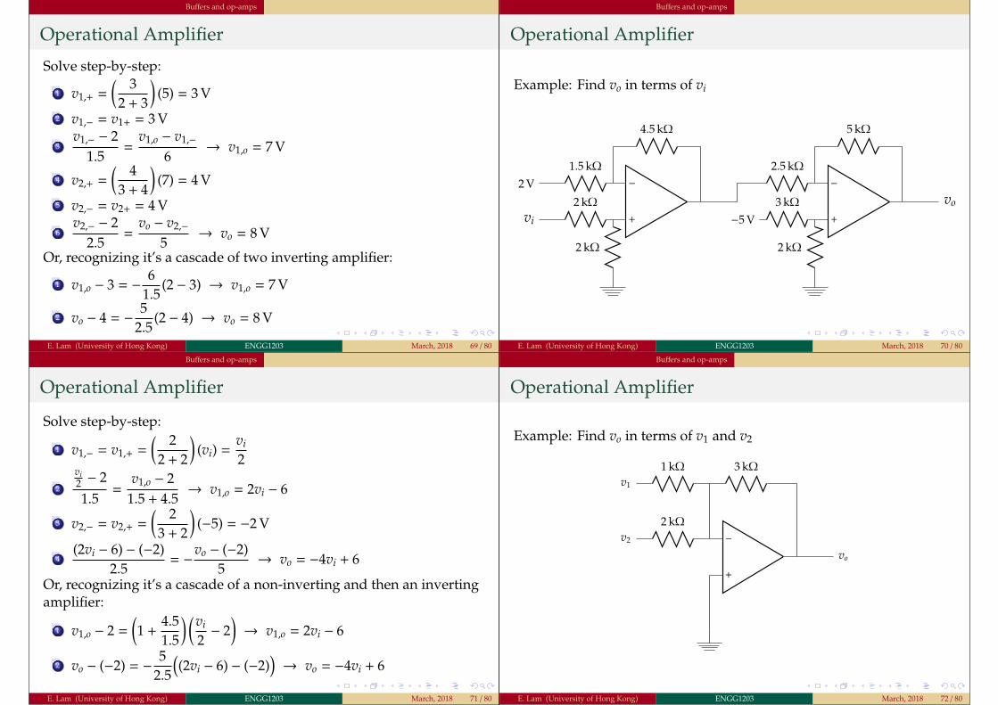
Buffers and op-amps
Operational Amplifier
Example: Find vo in terms of vi
−
+
1.5 kΩ
2 V
2 kΩ
vi
2 kΩ
4.5 kΩ
−
+
2.5 kΩ
3 kΩ
−5 V
2 kΩ
vo
5 kΩ
E. Lam (University of Hong Kong) ENGG1203 March, 2018 70 / 80
Buffers and op-amps
Operational Amplifier
Solve step-by-step:
1 v1,− = v1,+ =( 22 + 2
)(vi) =
vi
2
2
vi2 − 21.5
=v1,o − 2
1.5 + 4.5→ v1,o = 2vi − 6
3 v2,− = v2,+ =( 23 + 2
)(−5) = −2 V
4(2vi − 6) − (−2)
2.5= −vo − (−2)
5→ vo = −4vi + 6
Or, recognizing it’s a cascade of a non-inverting and then an invertingamplifier:
1 v1,o − 2 =(1 +
4.51.5
) (vi
2− 2
)→ v1,o = 2vi − 6
2 vo − (−2) = − 52.5
((2vi − 6) − (−2)
)→ vo = −4vi + 6
E. Lam (University of Hong Kong) ENGG1203 March, 2018 71 / 80
Buffers and op-amps
Operational Amplifier
Example: Find vo in terms of v1 and v2
−
+
2 kΩ
v2
1 kΩ
v1
3 kΩ
vo
E. Lam (University of Hong Kong) ENGG1203 March, 2018 72 / 80
Buffers and op-amps
Operational Amplifier
Solve step-by-step:1 v− = v+ = 02 By KCL at the negative terminal of the op-amp,
v1
1+
v2
2+
vo
3= 0
Therefore, vo = −3(v1 +
v2
2
).
Overall, we see op-amps can do many things, such as multiply, add,and buffer. . .
E. Lam (University of Hong Kong) ENGG1203 March, 2018 73 / 80
Integrated circuits
1 Big picture of engineering analysis
2 Building and analysis of electrical/electronic circuits
3 Circuit theorems: superposition, Thevenin, Norton
4 Interface with (digital) logic circuits
5 Buffers and op-amps
6 Integrated circuits
E. Lam (University of Hong Kong) ENGG1203 March, 2018 74 / 80
Integrated circuits
Opening Up an Op-amp
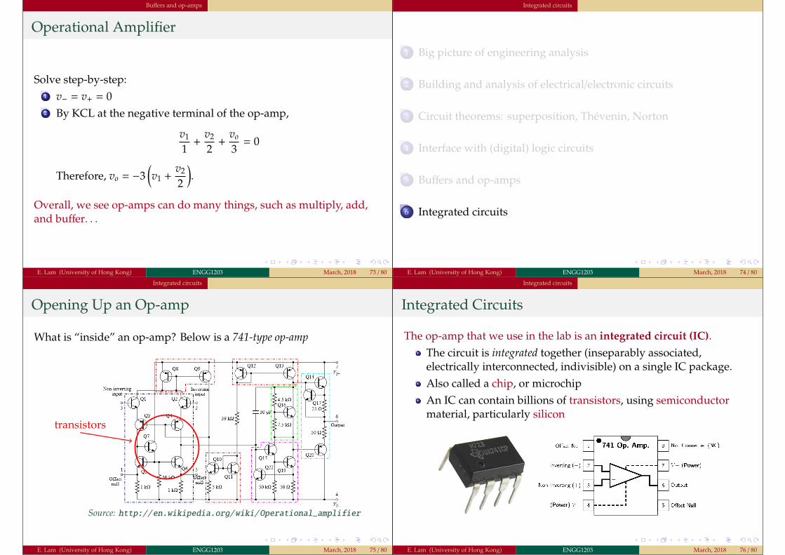
What is “inside” an op-amp? Below is a 741-type op-amp
Source: http://en.wikipedia.org/wiki/Operational_amplifier
transistors
E. Lam (University of Hong Kong) ENGG1203 March, 2018 75 / 80
Integrated circuits
Integrated Circuits
The op-amp that we use in the lab is an integrated circuit (IC).The circuit is integrated together (inseparably associated,electrically interconnected, indivisible) on a single IC package.Also called a chip, or microchipAn IC can contain billions of transistors, using semiconductormaterial, particularly silicon
E. Lam (University of Hong Kong) ENGG1203 March, 2018 76 / 80
Integrated circuits
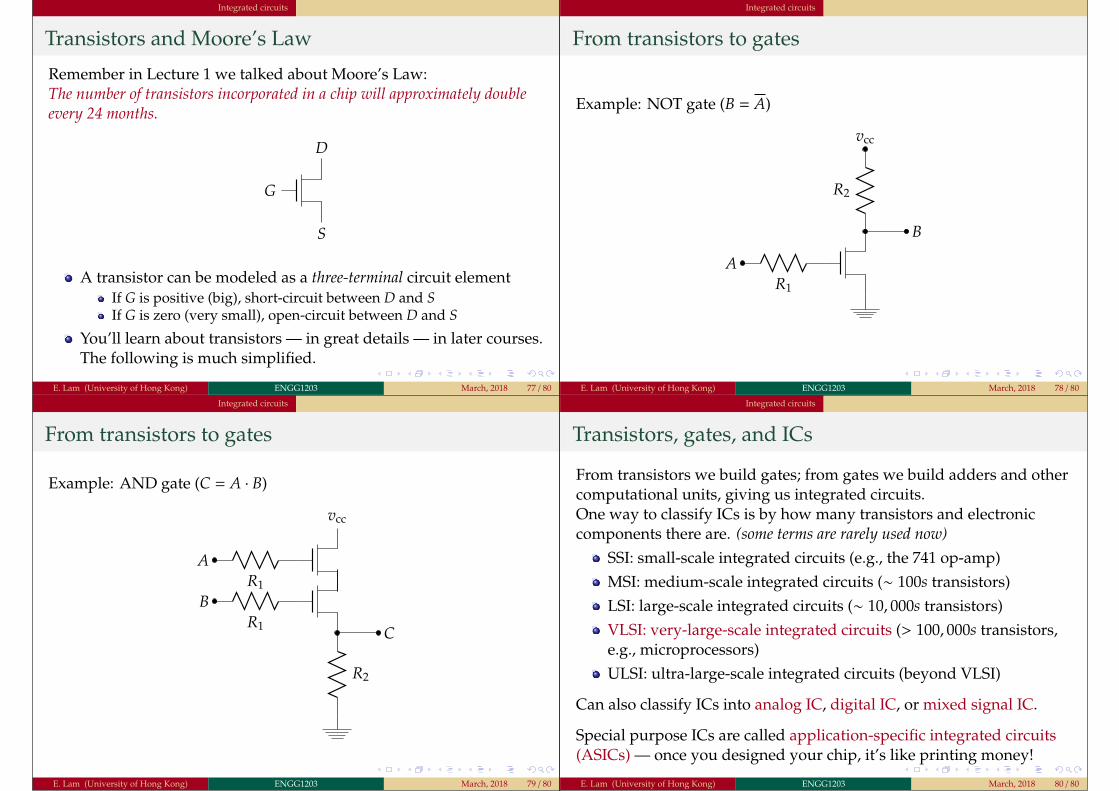
Transistors and Moore’s Law
Remember in Lecture 1 we talked about Moore’s Law:The number of transistors incorporated in a chip will approximately doubleevery 24 months.
G
D
S
A transistor can be modeled as a three-terminal circuit elementIf G is positive (big), short-circuit between D and SIf G is zero (very small), open-circuit between D and S
You’ll learn about transistors — in great details — in later courses.The following is much simplified.
E. Lam (University of Hong Kong) ENGG1203 March, 2018 77 / 80
Integrated circuits
From transistors to gates
Example: NOT gate (B = A)
R1
A
R2
vcc
B
E. Lam (University of Hong Kong) ENGG1203 March, 2018 78 / 80
Integrated circuits
From transistors to gates
Example: AND gate (C = A · B)
vcc
R1
A
R1
B
R2
C
E. Lam (University of Hong Kong) ENGG1203 March, 2018 79 / 80
Integrated circuits
Transistors, gates, and ICs
From transistors we build gates; from gates we build adders and othercomputational units, giving us integrated circuits.One way to classify ICs is by how many transistors and electroniccomponents there are. (some terms are rarely used now)
SSI: small-scale integrated circuits (e.g., the 741 op-amp)MSI: medium-scale integrated circuits (∼ 100s transistors)LSI: large-scale integrated circuits (∼ 10, 000s transistors)VLSI: very-large-scale integrated circuits (> 100, 000s transistors,e.g., microprocessors)ULSI: ultra-large-scale integrated circuits (beyond VLSI)
Can also classify ICs into analog IC, digital IC, or mixed signal IC.
Special purpose ICs are called application-specific integrated circuits(ASICs) — once you designed your chip, it’s like printing money!
E. Lam (University of Hong Kong) ENGG1203 March, 2018 80 / 80