electronic excitations in materials for solar cells - tddft. · pdf fileks green’s...
TRANSCRIPT

Electronic excitations in materials for solar cellsbeyond standard density functional theory
Silvana Botti
1LSI, Ecole Polytechnique-CNRS-CEA, Palaiseau, France2LPMCN, CNRS-Universite Lyon 1, France
3European Theoretical Spectroscopy Facility
October 21, 2010 – LASIM, Lyon
Silvana Botti Electronic excitations & photovoltaics 1 / 34

Outline
1 Electronic excitations: beyond standard DFT?
2 Band structuresChalcopyrite absorbersCu-based delafossite transparent conductive oxides
3 Optical spectra
4 Conclusions and perspectives
Silvana Botti Electronic excitations & photovoltaics 2 / 34

Problems of standard DFT
Modeling electronic excitations in complex systems
ObjectivesPredict accurate values forfundamental opto-electronicalproperties (gap, absorptionspectra, excitons, . . .)
Simulate real materials(nanostructured systems,large unit cells, defects,doping, interfaces, . . .)
Find a compromise between accuracy and computational effort
Silvana Botti Electronic excitations & photovoltaics 3 / 34
Problems of standard DFT
Density functional theory
In literature standard computational approach for band structures:
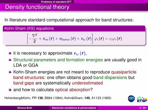
Kohn-Sham (KS) equations[−∇
2
2+ vext (r) + vHartree (r) + vxc (r)
]ϕi (r) = εiϕi (r)
it is necessary to approximate vxc (r),Structural parameters and formation energies are usually good inLDA or GGAKohn-Sham energies are not meant to reproduce quasiparticleband structures: one often obtains good band dispersions butband gaps are systematically underestimatedand how to calculate optical absorption?
Hohenberg&Kohn, PR 136, B864 (1964); Kohn&Sham, 140, A1133 (1965)
Silvana Botti Electronic excitations & photovoltaics 4 / 34

Problems of standard DFT
Density functional theory
In literature standard computational approach for band structures:
Kohn-Sham (KS) equations[−∇
2
2+ vext (r) + vHartree (r) + vxc (r)
]ϕi (r) = εiϕi (r)
it is necessary to approximate vxc (r),Structural parameters and formation energies are usually good inLDA or GGAKohn-Sham energies are not meant to reproduce quasiparticleband structures: one often obtains good band dispersions butband gaps are systematically underestimatedand how to calculate optical absorption?
Hohenberg&Kohn, PR 136, B864 (1964); Kohn&Sham, 140, A1133 (1965)
Silvana Botti Electronic excitations & photovoltaics 4 / 34

Problems of standard DFT
Excitation energies: photoemission
Photoemission process:
hν − (Ekin + φ) = EN−1,v − EN,0 = −εv
Silvana Botti Electronic excitations & photovoltaics 5 / 34

Problems of standard DFT
Excitation energies: photoemission
Inverse photoemission process:
hν − (Ekin + φ) = EN,0 − EN+1,c = −εc
Silvana Botti Electronic excitations & photovoltaics 5 / 34

Problems of standard DFT
Excitation energies: energy gap
Photoemission gap:Egap = I − A = mink ,l
(EN−1,k + EN+1,l − 2EN,0
)Silvana Botti Electronic excitations & photovoltaics 6 / 34

Problems of standard DFT
Excitation energies: energy gap
Optical gap:Egap = I − A− Eexc
binding
Silvana Botti Electronic excitations & photovoltaics 6 / 34

Problems of standard DFT
A intuitive path: propagation of electrons and holes
! "
! "#!
#" $" "" "!" "" "!
" "" "" " #
! "# " ! " " " " " "
#$" "" " #
! "# " ! " " " ! " "
#!" "" " #
! "%# ! "$ " " !" !" ! "
#!
!
Π0
!
! "&# $ " $ #
In the many-body Green’s function framework:GW for electron addition and removal(one-particle G)Bethe-Salpeter equation for the inclusion ofelectron-hole interaction (two-particle G)
The price to pay is a more involved theoretical andcomputational framework
L. Hedin, Phys. Rev. 139 (1965)
Silvana Botti Electronic excitations & photovoltaics 7 / 34

Problems of standard DFT
Green’s function and Hedin’s equations
Propagation of an extra particle (electron or hole):
G(r1, r2, t1 − t2) = −i〈N|T [ψ(r1, t1)ψ†(r2, t2)]|N〉
Electron density:
ρ (r) = G(r , r , t , t+)
Spectral function:
A(ω) = 1/πTr {Im G(r1, r2, ω)}
G has poles at addition and removal energies
Silvana Botti Electronic excitations & photovoltaics 8 / 34

Problems of standard DFT
Green’s function and Hedin’s equations
Propagation of an extra particle (electron or hole):
G(r1, r2, t1 − t2) = −i〈N|T [ψ(r1, t1)ψ†(r2, t2)]|N〉
Σ
G
ΓP
W
G=G 0+G 0 Σ G
Γ=1+
(δΣ/
δG)G
GΓ
P = GGΓ
W = v + vPW
Σ = GWΓ
P = GG
Hedin’s equationsshould be solvedself-consistently
Silvana Botti Electronic excitations & photovoltaics 8 / 34

Problems of standard DFT
Self-energy and screened interaction
Self-energy: nonlocal, non-Hermitian, frequency dependent operatorIt allows to obtain the Green’s function G once that G0 is known
Hartree-Fock Σx (r1, r2) = iG(r1, r2, t , t+)v(r1, r2)
GW Σ(r1, r2, t1 − t2) = iG(r1, r2, t1 − t2)W (r1, r2, t2 − t1)
W = ε−1v : screened potential (much weaker than v !)
Ingredients:KS Green’s function G0, and RPA dielectric matrix ε−1
G,G′(q, ω)
L. Hedin, Phys. Rev. 139 (1965)
Silvana Botti Electronic excitations & photovoltaics 9 / 34

Band structures Chalcopyrite absorbers
2 Band structuresChalcopyrite absorbersCu-based delafossite transparent conductive oxides
J. Vidal, S. Botti, P. Olsson, J.-F. Guillemoles, and L. Reining, “Strong interplaybetween structure and electronic properties in CuIn(S,Se)2: a first-principlesstudy ”, Phys. Rev. Lett. 104, 056401 (2010).
I. Aguilera, S. Botti, J. Vidal, P. Wahnon, and L. Reining, “Band structure andoptical absorption of CuGaS2: a self-consistent GW study”, to be submitted(2010).
J. Vidal, “Ab initio Calculations of the Electronic Properties of CuIn(S,Se)2 andother Materials for Photovoltaic Applications”, Ph.D. Thesis, Ecole Polytechnique,France (2010).
Silvana Botti Electronic excitations & photovoltaics 10 / 34

Band structures Chalcopyrite absorbers
Present state of photovoltaic efficiency
Silvana Botti Electronic excitations & photovoltaics 11 / 34

Band structures Chalcopyrite absorbers
CIGS solar cell
Devices have to fulfill 2 functions:Photogeneration of electron-hole pairsSeparation of charge carriers to generate a current
Structure:
Molybdenum back contactCIGS layer (p-type layer)CdS layer (n-type layer)ZnO:Al TCO contact
Wurth Elektronik GmbH & Co.Efficiency = 13 %
Silvana Botti Electronic excitations & photovoltaics 12 / 34

Band structures Chalcopyrite absorbers
Energy converted by a silicon solar cell
Carriers below the gap are not absorbed
Silvana Botti Electronic excitations & photovoltaics 13 / 34

Band structures Chalcopyrite absorbers
CIGS properties
Cu(In,Ga)(S,Se)2 absorbers:
high optical absorption⇒ thin-layer filmsoptimal photovoltaic gap(record efficiency 20.1%)self-doping with native defects⇒ p-n junctionsextraordinary stability underoperating conditions: tolerance tolarge off-stoichiometries, stress,defects (not well understood) 1 1.2 1.4 1.6 1.8 2
Eg [eV]
8
10
12
14
16
18
20
η [%
]
CuGaSe2
CuInS2
CuInSe2
Cu(In,Ga)Se2
Silvana Botti Electronic excitations & photovoltaics 14 / 34

Band structures Chalcopyrite absorbers
LDA energies for CIS
CuInS2DFT-LDA G0W0 exp.
Eg -0.11 0.28 1.54In-S 6.5 6.9 6.9
S s band 12.4 13.0 12.0In 4 d band 14.6 16.4 18.2
CuInSe2DFT-LDA G0W0 exp.
Eg -0.29 0.25 1.05In-Se 5.8 6.15 6.5
Se s band 12.6 12.9 13.0In 4 d band 14.7 16.2 18.0
www.abinit.org
Silvana Botti Electronic excitations & photovoltaics 15 / 34
Band structures Chalcopyrite absorbers
Perturbative GW: “best G, best W”
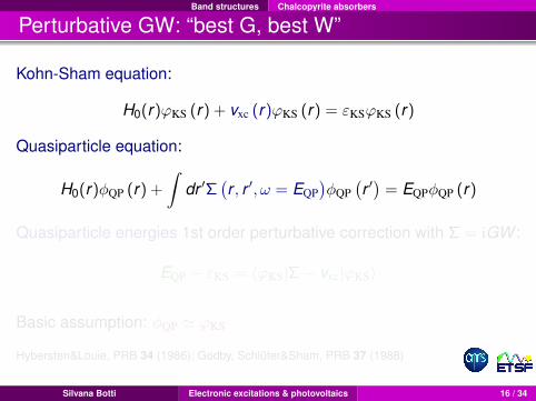
Kohn-Sham equation:
H0(r)ϕKS (r) + vxc (r)ϕKS (r) = εKSϕKS (r)
Quasiparticle equation:
H0(r)φQP (r) +
∫dr ′Σ
(r , r ′, ω = EQP
)φQP
(r ′)
= EQPφQP (r)
Quasiparticle energies 1st order perturbative correction with Σ = iGW :
EQP − εKS = 〈ϕKS|Σ− vxc|ϕKS〉
Basic assumption: φQP ' ϕKS
Hybersten&Louie, PRB 34 (1986); Godby, Schluter&Sham, PRB 37 (1988)
Silvana Botti Electronic excitations & photovoltaics 16 / 34

Band structures Chalcopyrite absorbers
Perturbative GW: “best G, best W”
Kohn-Sham equation:
H0(r)ϕKS (r) + vxc (r)ϕKS (r) = εKSϕKS (r)
Quasiparticle equation:
H0(r)φQP (r) +
∫dr ′Σ
(r , r ′, ω = EQP
)φQP
(r ′)
= EQPφQP (r)
Quasiparticle energies 1st order perturbative correction with Σ = iGW :
EQP − εKS = 〈ϕKS|Σ− vxc|ϕKS〉
Basic assumption: φQP ' ϕKS
Hybersten&Louie, PRB 34 (1986); Godby, Schluter&Sham, PRB 37 (1988)
Silvana Botti Electronic excitations & photovoltaics 16 / 34

Band structures Chalcopyrite absorbers
G0W0 energies for CIS
CuInS2DFT-LDA G0W0 exp.
Eg -0.11 0.28 1.54In-S 6.5 6.9 6.9
S s band 12.4 13.0 12.0In 4 d band 14.6 16.4 18.2
CuInSe2DFT-LDA G0W0 exp.
Eg -0.29 0.25 1.05In-Se 5.8 6.15 6.5
Se s band 12.6 12.9 13.0In 4 d band 14.7 16.2 18.0
www.abinit.org
Silvana Botti Electronic excitations & photovoltaics 17 / 34

Band structures Chalcopyrite absorbers
Beyond Standard GW
Looking for another starting point:DFT with another approximation for vxc : GGA, EXX,...(e.g. Rinke et al. 2005)LDA/GGA + U (e.g. Kioupakis et al. 2008, Jiang et al. 2009 )Hybrid functionals (e.g. Fuchs et al. 2007)
EPBE0xc = EPBE
xc +14(EHF
x − EPBEx)
Silvana Botti Electronic excitations & photovoltaics 18 / 34

Band structures Chalcopyrite absorbers
Beyond Standard GW
Looking for another starting point:DFT with another approximation for vxc : GGA, EXX,...(e.g. Rinke et al. 2005)LDA/GGA + U (e.g. Kioupakis et al. 2008, Jiang et al. 2009 )Hybrid functionals (e.g. Fuchs et al. 2007)
Self-consistent approaches:GWscQP scheme (Faleev et al. 2004)scCOHSEX scheme (Hedin 1965, Bruneval et al. 2005)
Our choice is to get a better starting point for G0W0 using scCOHSEX
Silvana Botti Electronic excitations & photovoltaics 18 / 34

Band structures Chalcopyrite absorbers
COHSEX: approximation to GW self-energy
Statically screened exchange:
ΣSEX(r1, r2) = −∑
i
θ(µ− Ei)φi(r1)φ∗i (r2)W (r1, r2, ω = 0)
Induced classical potential due to an extra point charge:
ΣCOH(r1, r2) =12δ(r1 − r2)[W (r1, r2, ω = 0)− v(r1, r2)]
L. Hedin and S. Lundqvist, Solid State Phys. 23, 1 (1969);
Bruneval et al. PRL 97, 267601 (2006); Gatti et al. PRL 99, 266402 (2007)
Silvana Botti Electronic excitations & photovoltaics 19 / 34

Band structures Chalcopyrite absorbers
Quasiparticle energies within sc-GW for CIS
CuInS2DFT-LDA G0W0 sc-GW exp.
Eg -0.11 0.28 1.48 1.54In-S 6.5 6.9 7.0 6.9
S s band 12.4 13.0 13.6 12.0In 4 d band 14.6 16.4 18.2 18.2
CuInSe2DFT-LDA G0W0 sc-GW exp.
Eg -0.29 0.25 1.14 1.05 (+0.2)In-Se 5.8 6.15 6.64 6.5
Se s band 12.6 12.9 13.6 13.0In 4 d band 14.7 16.2 17.8 18.0
sc-GW is here sc-COHSEX+G0W0
www.abinit.org
Silvana Botti Electronic excitations & photovoltaics 20 / 34

Band structures Chalcopyrite absorbers
Band structures of CuGaSe2
T Γ N-16
-14
-12
-10
-8
-6
-4
-2
0
2
4
6
8
Ene
rgy
(eV
)
LDAscCOHSEX+G
0W
0
Se 4s
Ga-Se bond
Cu 3d - Se 4p
Comparison of LDA (red) andscGW (blue) bands of CuGaSe2
Analogous results for CuGaS2
No need to include the delectrons of Ga in the valenceAgreement with experimentalgap within less than 0.1 eV
Silvana Botti Electronic excitations & photovoltaics 21 / 34

Band structures Chalcopyrite absorbers
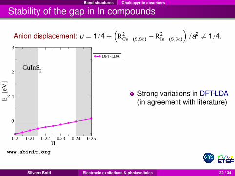
Stability of the gap in In compounds
Anion displacement: u = 1/4 +(
R2Cu−(S,Se) − R2
In−(S,Se)
)/a2 6= 1/4.
1. Experiments measure the same value for the gap (within 10%)
0.22 0.23 0.24u
5.6
5.7
5.8
5.9
6
a [Å
]
GGA
LDA
PBE0HSE06
B3LYP
HF+cHSE03
0 0.2 0.4 0.6 0.8 1b
0.22
0.23
0.24
u
2. The experimental dispersion ofu is, however, large
Only hybrid functionals givestructural parameters whichoverlap with experiments
Jaffe, PRB 29, 1882 (1984); Merino, J. Appl. Phys. 80, 5610 (1996)Jaffe, PRB 27, 5176 (1983); Jiang, Sem. Sci. Technol. 23, 025001 (2008)
Silvana Botti Electronic excitations & photovoltaics 22 / 34
Band structures Chalcopyrite absorbers
Stability of the gap in In compounds
Anion displacement: u = 1/4 +(
R2Cu−(S,Se) − R2
In−(S,Se)
)/a2 6= 1/4.
0.2 0.21 0.22 0.23 0.24 0.25u
0
1
2
3
Eg [
eV]
CuInS2
DFT-LDA
Strong variations in DFT-LDA(in agreement with literature)
www.abinit.org
Silvana Botti Electronic excitations & photovoltaics 22 / 34

Band structures Chalcopyrite absorbers
Stability of the gap in In compounds
Anion displacement: u = 1/4 +(
R2Cu−(S,Se) − R2
In−(S,Se)
)/a2 6= 1/4.
0.2 0.21 0.22 0.23 0.24 0.25u
0
1
2
3
Eg [
eV]
CuInS2
DFT-LDAG
0W
0
G0W0 does not change theslope . . .
www.abinit.org
Silvana Botti Electronic excitations & photovoltaics 22 / 34

Band structures Chalcopyrite absorbers
Stability of the gap in In compounds
Anion displacement: u = 1/4 +(
R2Cu−(S,Se) − R2
In−(S,Se)
)/a2 6= 1/4.
0.2 0.21 0.22 0.23 0.24 0.25u
0
1
2
3
Eg [
eV]
CuInS2
DFT-LDAG
0W
0
. . . except if the gap is alreadyopen
www.abinit.org
Silvana Botti Electronic excitations & photovoltaics 22 / 34

Band structures Chalcopyrite absorbers
Stability of the gap in In compounds
Anion displacement: u = 1/4 +(
R2Cu−(S,Se) − R2
In−(S,Se)
)/a2 6= 1/4.
0.2 0.21 0.22 0.23 0.24 0.25u
0
1
2
3
Eg [
eV]
CuInS2
DFT-LDAG
0W
0scGW
sc-GW enhances the gapvariation
www.abinit.org
Silvana Botti Electronic excitations & photovoltaics 22 / 34
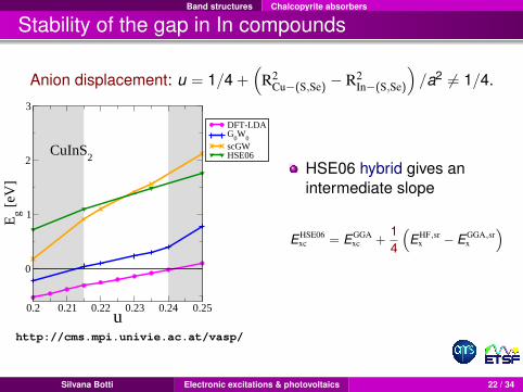
Band structures Chalcopyrite absorbers
Stability of the gap in In compounds
Anion displacement: u = 1/4 +(
R2Cu−(S,Se) − R2
In−(S,Se)
)/a2 6= 1/4.
0.2 0.21 0.22 0.23 0.24 0.25u
0
1
2
3
Eg [
eV]
CuInS2
DFT-LDAG
0W
0scGWHSE06
HSE06 hybrid gives anintermediate slope
EHSE06xc = EGGA
xc +14
“EHF,sr
x − EGGA,srx
”
http://cms.mpi.univie.ac.at/vasp/
Silvana Botti Electronic excitations & photovoltaics 22 / 34

Band structures Chalcopyrite absorbers
Stability of the gap in In compounds
Anion displacement: u = 1/4 +(
R2Cu−(S,Se) − R2
In−(S,Se)
)/a2 6= 1/4.
0.2 0.21 0.22 0.23 0.24 0.25u
0
1
2
3
Eg [
eV]
CuInS2
DFT-LDAG
0W
0scGWHSE06HSE06 ε
0
a modified-HSE06 (the mixingparameter of the screenedFock exchange is proportionalto the screening) gives thesc-GW slope
http://cms.mpi.univie.ac.at/vasp/
Silvana Botti Electronic excitations & photovoltaics 22 / 34

Band structures Chalcopyrite absorbers
Stability of the gap in In compounds
Anion displacement: u = 1/4 +(
R2Cu−(S,Se) − R2
In−(S,Se)
)/a2 6= 1/4.
Is the gap stable under lattice distortion?
sc-GW and hybrid calculations predict even stronger variationsthan LDAThe gap is not stable under lattice distortion alone
Silvana Botti Electronic excitations & photovoltaics 22 / 34

Band structures Chalcopyrite absorbers
Formation energy of Cu vacancies
The formation energy of VCu varies under lattice distortion:
∆Ef = ∆EDFTf −∆Esc−GW
VBM
Silvana Botti Electronic excitations & photovoltaics 23 / 34

Band structures Chalcopyrite absorbers
Formation energy of Cu vacancies
The formation energy of VCu varies under lattice distortion:
∆Ef = ∆EDFTf −∆Esc−GW
VBM
conduction band minimum (CBM)
valence band maximum (VBM)
It is essential to go beyond DFT-LDALDA+U (blue lines) gives only constant shifts
Zhang et al. PRB 57, 9642 (1998); Lany et al. PRB 78, 235104 (2008).
Silvana Botti Electronic excitations & photovoltaics 23 / 34

Band structures Chalcopyrite absorbers
Why is the experimental gap so stable?
A feedback loop can explain the stability of the band gap:
∆u ∆Eg
∆Hf(V
Cu) ∆[V
Cu]
∆Eg
Silvana Botti Electronic excitations & photovoltaics 24 / 34

Band structures Chalcopyrite absorbers
Why is the experimental gap so stable?
A feedback loop can explain the stability of the band gap:
∆u ∆Eg
∆Hf(V
Cu) ∆[V
Cu]
∆Eg
-3 -2.5 -2 -1.5 -1ln([V
Cu]/N
Cu)
1
1.1
1.2
1.3
1.4
Eg [
eV]
Eg=1.6663+0.231*ln([V
Cu]/N
Cu)
0.2 0.21 0.22 0.23 0.24 0.25u
0
0.5
1
1.5
2
2.5
3
Eg [
eV]
Eg=-5.975+32.1*u
0.2 0.21 0.22 0.23 0.24 0.25u
-0.6
-0.5
-0.4
-0.3
-0.2
-0.1
0
∆VB
M [
eV] ∆E
v
scGW= 2.1335-11.06*u
Silvana Botti Electronic excitations & photovoltaics 24 / 34

Band structures Chalcopyrite absorbers
Why is the experimental gap so stable?
A feedback loop can explain the stability of the band gap:
∆u ∆Eg
∆Hf(V
Cu) ∆[V
Cu]
∆Eg
Experimental variation of u is 0.02⇒ ∆Eg ≈ 0.65 eVConsidering variations of u and [VCu]⇒ ∆Eg ≈ -0.04 eV
Silvana Botti Electronic excitations & photovoltaics 24 / 34

Band structures Cu delafossites TCOs
2 Band structuresChalcopyrite absorbersCu-based delafossite transparent conductive oxides
J. Vidal, F. Trani, F. Bruneval, M. A. L. Marques and S. Botti, “Effects ofpolarization on the band-structure of delafossite transparent conductive oxides”,Phys. Rev. Lett. 104, 136401 (2010).
F. Trani, J. Vidal, S. Botti and M. A. L. Marques, “Band structures of delafossitetransparent conductive oxides from a self-consistent GW approach ”, Phys. Rev.B 82, 085115 (2010).
Silvana Botti Electronic excitations & photovoltaics 25 / 34

Band structures Cu delafossites TCOs
Delafossite TCO properties
Cu(Al,In,Ga)O2 thin-films are transparent and conducting:
p-type or even bipolar conductivitycombination of n- and p-type TCO materials allows
→ stacked cells with increased efficiency→ functional windows→ transparent transistors
Silvana Botti Electronic excitations & photovoltaics 26 / 34

Band structures Cu delafossites TCOs
The long dispute about delafossite gaps
LDA LDA+U B3LYP HSE03 HSE06 G0W
0scGW scGW+P0
1
2
3
4
5
6
Eg [
eV]
Eg
indirect
Eg
direct
∆=Eg
direct-E
g
indirect
exp. direct gap
exp. indirectgap
Experimental dataare for optical gap:exciton bindingenergy ≈ 0.5 eV[Laskowski et al. PRB 79,
165209 (2009)]
Strong latticepolaron effects areexpected ≈ 1 eV[Bechstedt et al. PRB 72,
245114 (2005)]
Silvana Botti Electronic excitations & photovoltaics 27 / 34

Band structures Cu delafossites TCOs
Comparison with hybrid functional calculations
Γ F L Z Γ-2.0
0.0
2.0
4.0
6.0
8.0
Ene
rgy(
eV)
sc-GW
Γ F L Z Γ
HSE03
Γ F L Z Γ
LDA+U
Strong differences both in dispersion and energy gapsAre hybrids a good compromise?
Silvana Botti Electronic excitations & photovoltaics 28 / 34

Optical spectra
Bethe-Salpeter equation: electron-hole interaction
The BSE for the reducible 4-point polarizability L:
L = L0 + L0
(4v −4 W
)L
4v(1, 2, 3, 4) = δ(1, 2)δ(3, 4)v(1, 3) and 4W = δ(1, 3)δ(2, 4)W (1, 2)
The measurable χ is obtained via a two-point contraction of L
χred(1,2) = −L(1,1,2,2)
In transition space and using the only-resonant approximation:
H2p,exc(vc)(v ′c′)A
v ′c′
λ = Eexcλ Av ′c′
λ
The ingredients are:Kohn-Sham wavefunctions and energiesGW corrected energiesscreening matrix ε−1
GG′(q)
Salpeter and Bethe, Phys. Rev. 84, 1232 (1951)Silvana Botti Electronic excitations & photovoltaics 29 / 34

Optical spectra
Optical absorption of CuGaS2
Excitonic binding energy of about 0.05 eVExperimental optical gap at 2.5 eV
2 3 4 5Energy (eV)
0
5
10
15
20O
ptic
al a
bsor
ptio
n
scGW gap
⊥||
Exp. 1
Exp. 2
BSE calculations
www.yambo-code.org
Silvana Botti Electronic excitations & photovoltaics 30 / 34

Optical spectra
Optical absorption of CuInO2
Strong excitonic effects also for the In compoundExp. absorption edge at 3.9 eVPolaronic effects should also be strong
0
5
10
15
20
0
5
10
15
20
ε 2
0 1 2 3 4 5 6 7 8Energy (eV)
0
5
10
15
20
RPA (NLF)
scGW(NLF)
scGW+BSE
solid lines: xy component, dashed: z component
www.yambo-code.org
Silvana Botti Electronic excitations & photovoltaics 31 / 34

Conclusions and perspectives
Conclusions and perspectives
Interpretation of experiments is often not straightforward – manycoupled effects!
Methods that go beyond ground-state DFT are by now well established
A better starting point than LDA is absolutely necessary for d-electronsSelf-consistent COHSEX+G0W0 gives a very good description ofquasi-particle statesHybrid functionals can be a good compromiseLDA+U does not work when there is hybridization of p − d states
In progress now:Absorption spectra from the Bethe-Salpeter equation for allcompoundsDefects using VASP and “improved” hybrid functionals
Silvana Botti Electronic excitations & photovoltaics 32 / 34

Conclusions and perspectives
Building-Integrated Photovoltaics
Projects realised so far do not yet represent the full range ofproducts available on the market: these include integratablecrystalline modules, thin-layer modules, transparent and shadingmodules, solar roof tiles, photovoltaic roof foils or complete solarroofsPlaying with light and glass: building-integrated photovoltaicsopens new creative opportunities for architects
Silvana Botti Electronic excitations & photovoltaics 33 / 34

Thanks!
Thanks to all collaborators! Thank you!
LSI – Ecole Polytechnique
Lucia Reining
Julien Vidal
Irene Aguilera
IRDEP – Paris
J.-F. Guillemoles
Par Olsson
LPMCN – Universite Lyon 1
Miguel Marques
Fabio Trani
Guilherme Vilhena
David Kammerlander
CEA – Saclay
Fabien Bruneval
http://www.etsf.euhttp://www.abinit.orgwww.yambo-code.org
Silvana Botti Electronic excitations & photovoltaics 34 / 34