electronic manufacturing v3.0 - fab academy 2016
TRANSCRIPT
1
Electronic Manufacturing Eric Pan
seeed.cc
p.seeed.cc
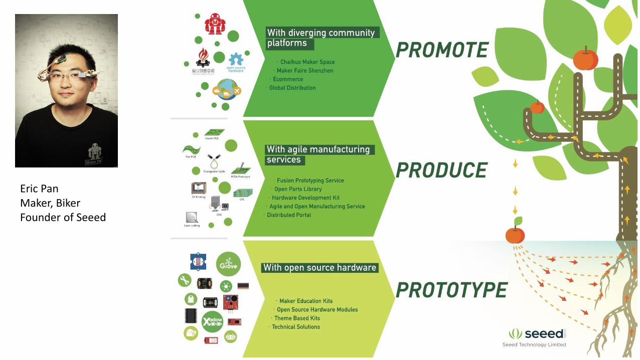
Eric PanMaker, BikerFounder of Seeed

3
Chapter 0
Overview
p.seeed.cc
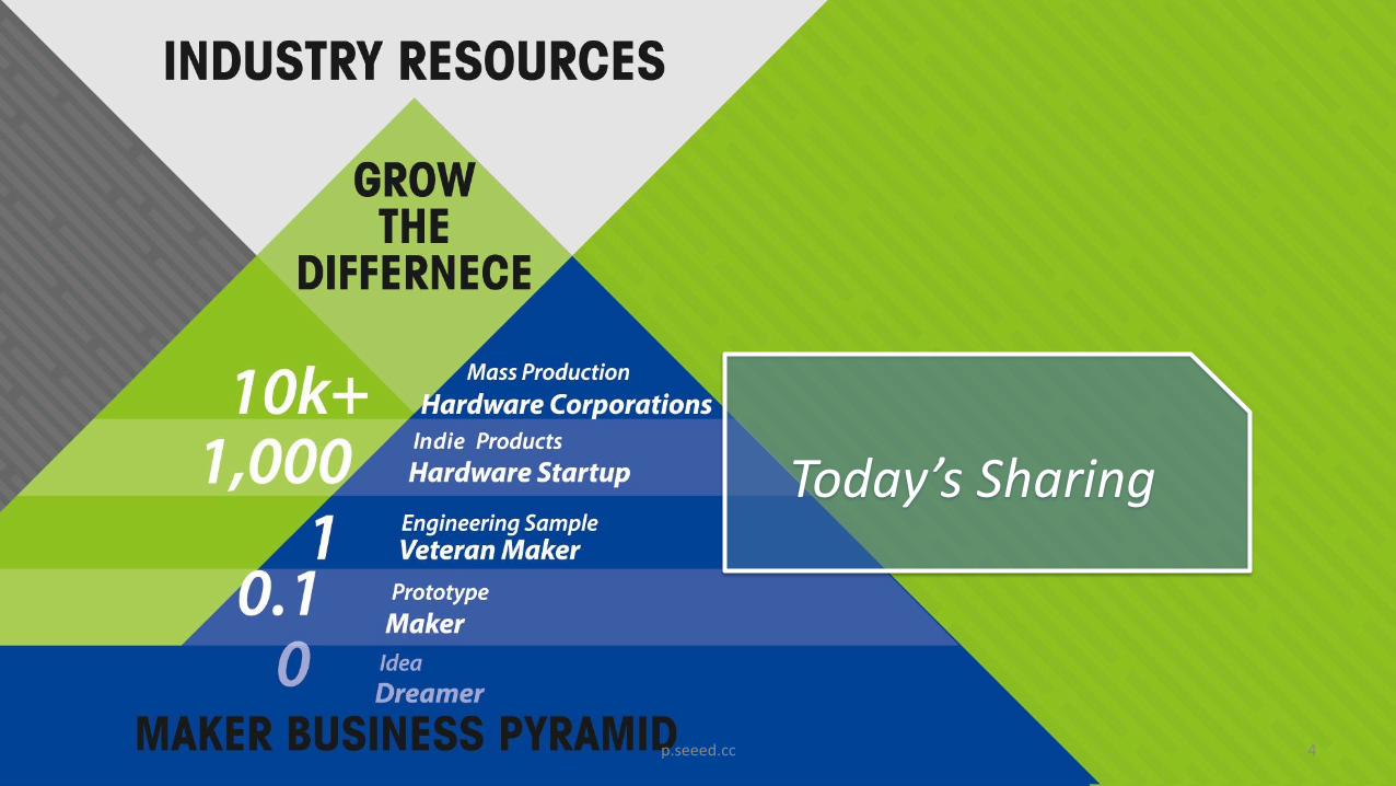
Today’s Sharing
4p.seeed.cc

HOW?
5p.seeed.cc
6
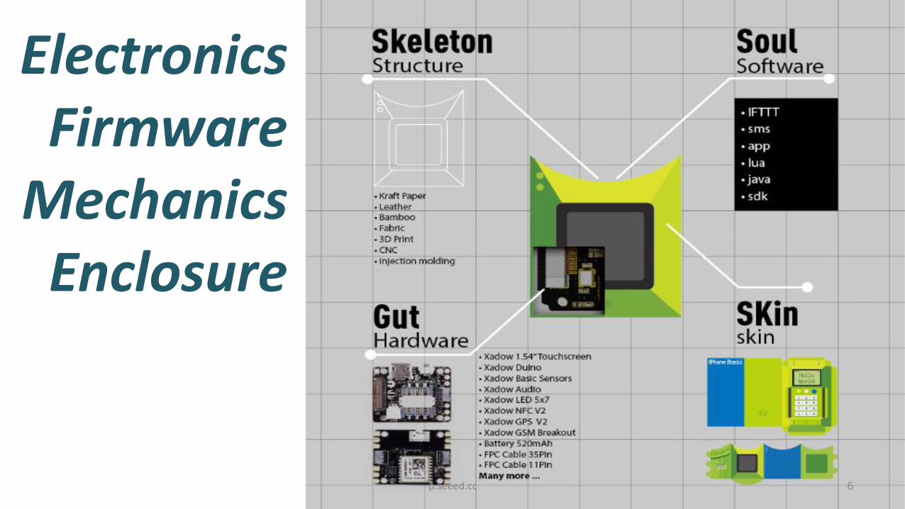
Electronics Firmware
MechanicsEnclosure
p.seeed.cc
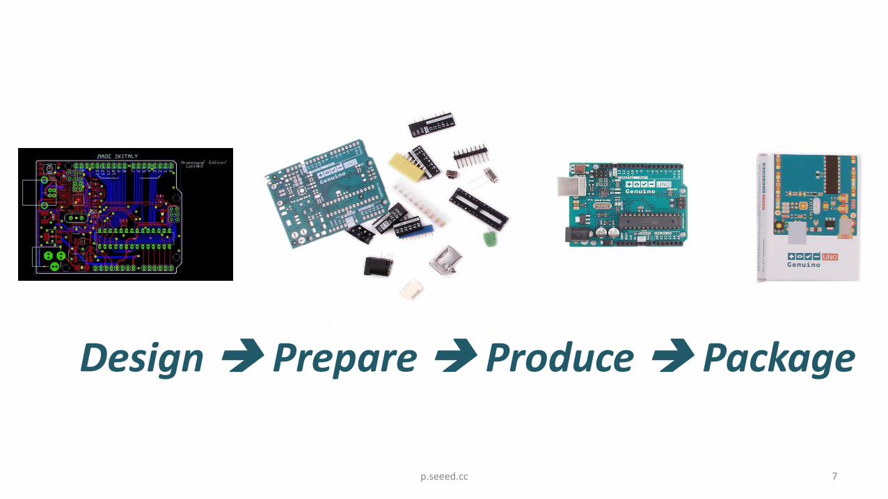
Design Prepare Produce Package
7p.seeed.cc
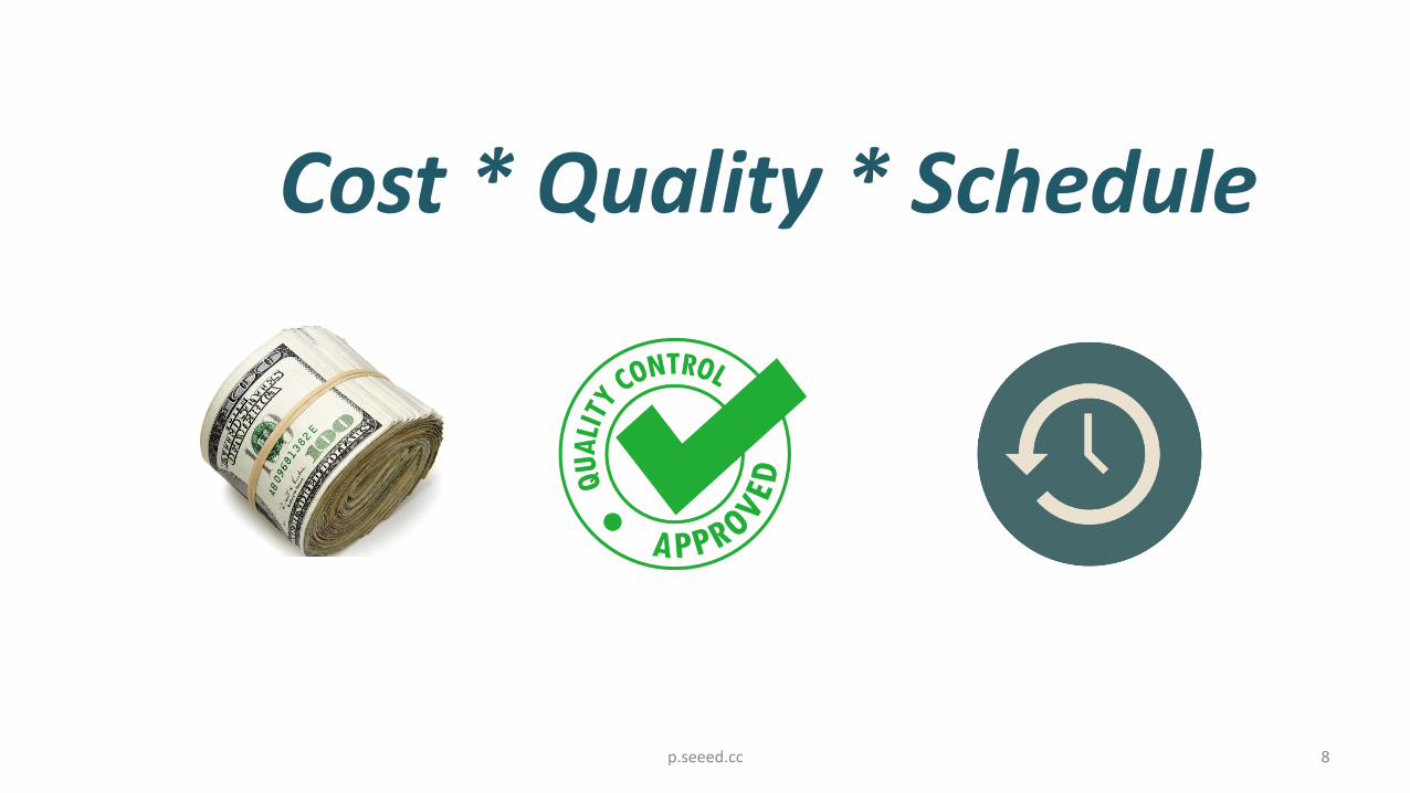
Cost * Quality * Schedule
8p.seeed.cc
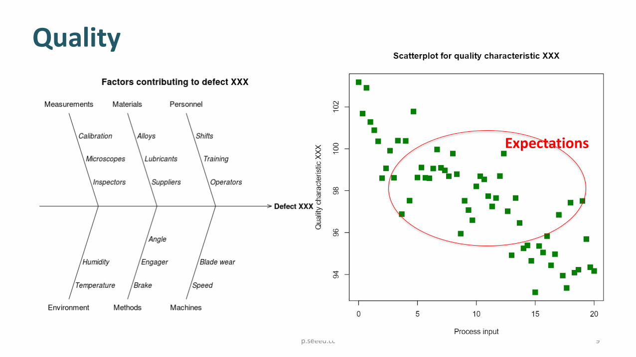
Quality
p.seeed.cc 9
Expectations
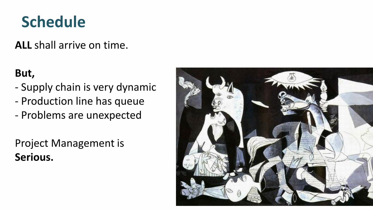
Schedule
ALL shall arrive on time.
But,- Supply chain is very dynamic- Production line has queue- Problems are unexpected
Project Management is Serious.
p.seeed.cc 10
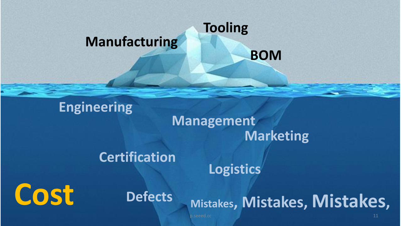
11p.seeed.cc
Cost
BOMManufacturing
Engineering
Marketing
CertificationLogistics
Defects
Management
Mistakes, Mistakes, Mistakes,
Tooling
12
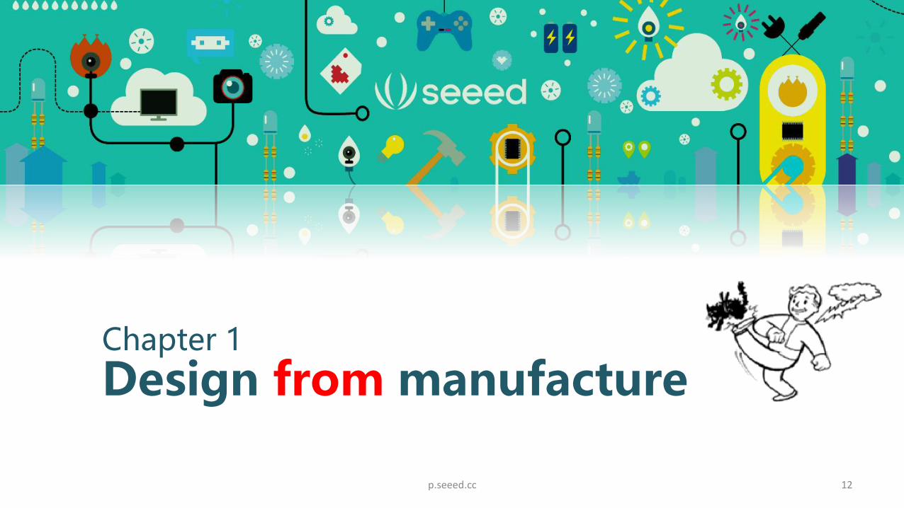
Chapter 1
Design from manufacture
p.seeed.cc
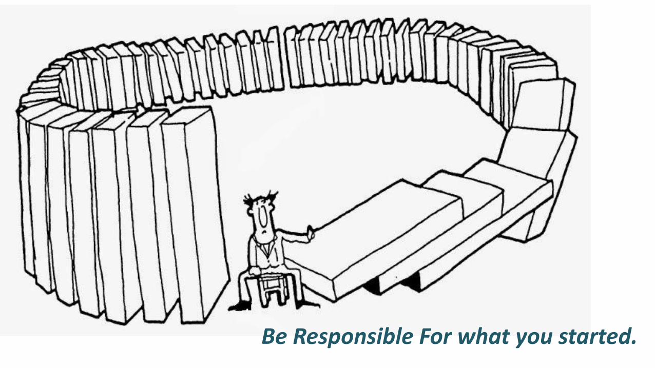
Be Responsible For what you started.
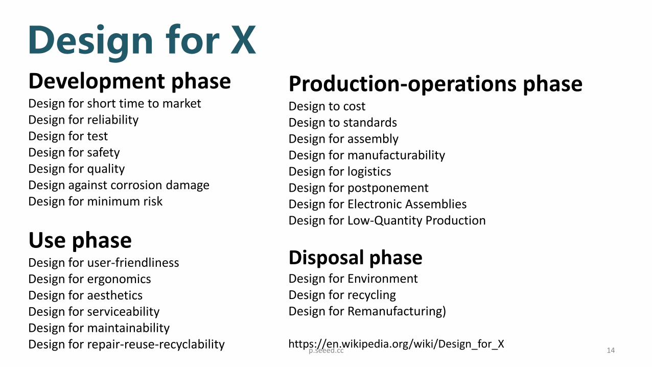
p.seeed.cc 14https://en.wikipedia.org/wiki/Design_for_X
Development phaseDesign for short time to marketDesign for reliabilityDesign for testDesign for safety Design for quality Design against corrosion damageDesign for minimum risk
Production-operations phaseDesign to costDesign to standardsDesign for assemblyDesign for manufacturabilityDesign for logisticsDesign for postponement Design for Electronic AssembliesDesign for Low-Quantity Production
Use phaseDesign for user-friendlinessDesign for ergonomicsDesign for aesthetics Design for serviceabilityDesign for maintainabilityDesign for repair-reuse-recyclability
Disposal phaseDesign for EnvironmentDesign for recyclingDesign for Remanufacturing)
Design for X

15
Hardware
OrchestraSoftware
Band
Unarmed to the new field.

p.seeed.cc 16https://en.wikipedia.org/wiki/Design_for_X
Development phaseDesign for short time to marketDesign for reliabilityDesign for testDesign for safety Design for quality Design against corrosion damageDesign for minimum risk
Production-operations phaseDesign to costDesign to standardsDesign for assemblyDesign for manufacturabilityDesign for logisticsDesign for postponement Design for Electronic AssembliesDesign for Low-Quantity Production
Use phaseDesign for user-friendlinessDesign for ergonomicsDesign for aesthetics Design for serviceabilityDesign for maintainabilityDesign for repair-reuse-recyclability
Disposal phaseDesign for EnvironmentDesign for recyclingDesign for Remanufacturing)
Design for X
17
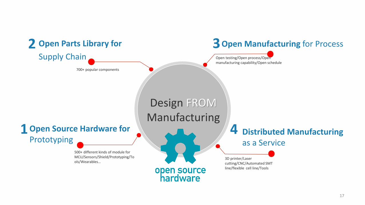
Design FROMManufacturing
700+ popular components
Open testing/Open process/Open manufacturing capability/Open schedule
3D printer/Laser cutting/CNC/Automated SMT line/flexible cell line/Tools
500+ different kinds of module for MCU/Sensors/Shield/Prototyping/Tools/Wearables…
Open Parts Library for
Supply Chain
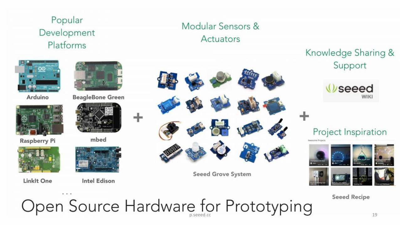
Open Source Hardware for Prototyping
Open Manufacturing for Process
Distributed Manufacturing as a Service
1
2 3
4
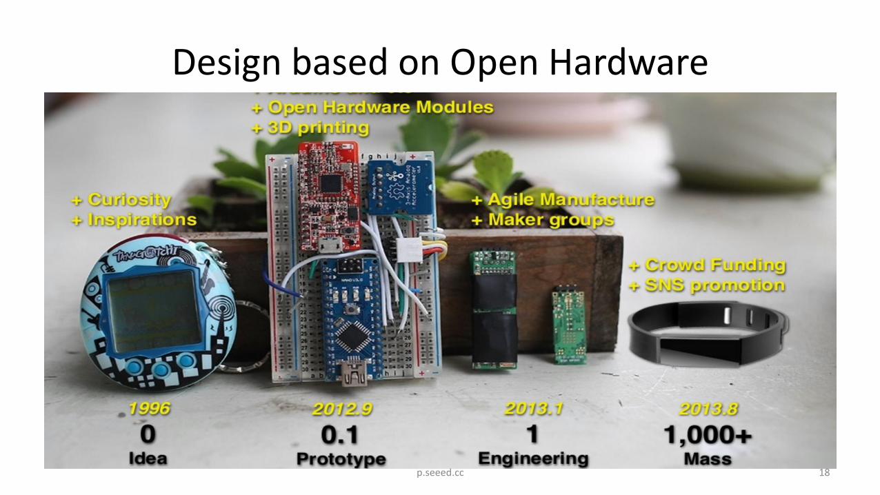
Design based on Open Hardware
18p.seeed.cc
19p.seeed.cc
20p.seeed.cc
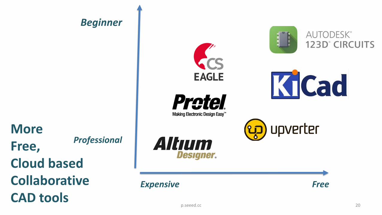
Beginner
Professional
Expensive Free
More Free, Cloud basedCollaborative CAD tools
21p.seeed.cc
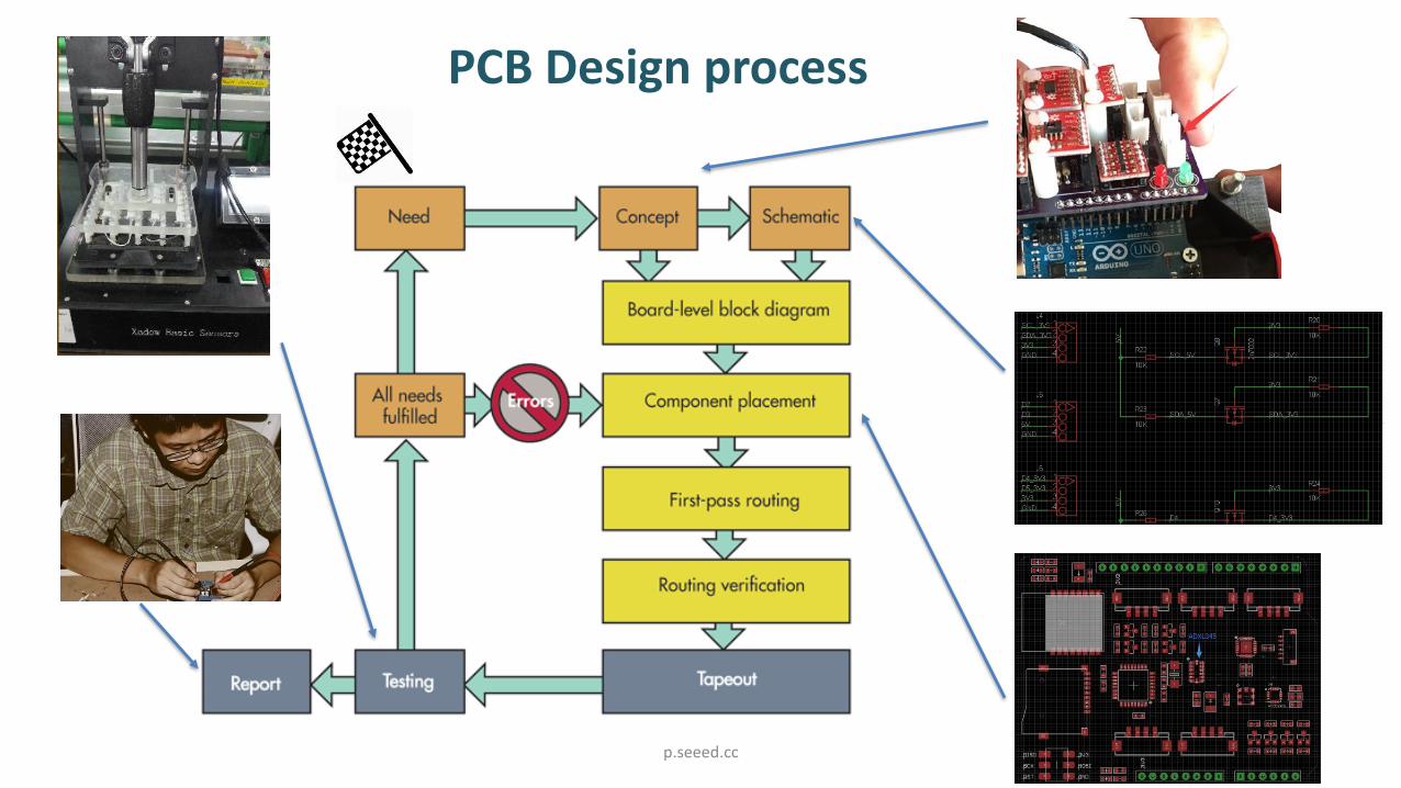
PCB Design process
22
Chapter 2
Prepare the materials
p.seeed.cc
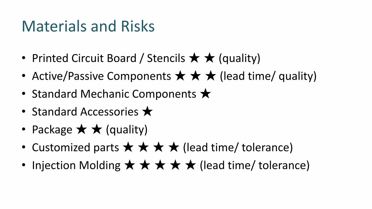
Materials and Risks
• Printed Circuit Board / Stencils ★★ (quality)
• Active/Passive Components ★★★ (lead time/ quality)
• Standard Mechanic Components ★
• Standard Accessories ★
• Package ★★ (quality)
• Customized parts ★★★★ (lead time/ tolerance)
• Injection Molding ★★★★★ (lead time/ tolerance)
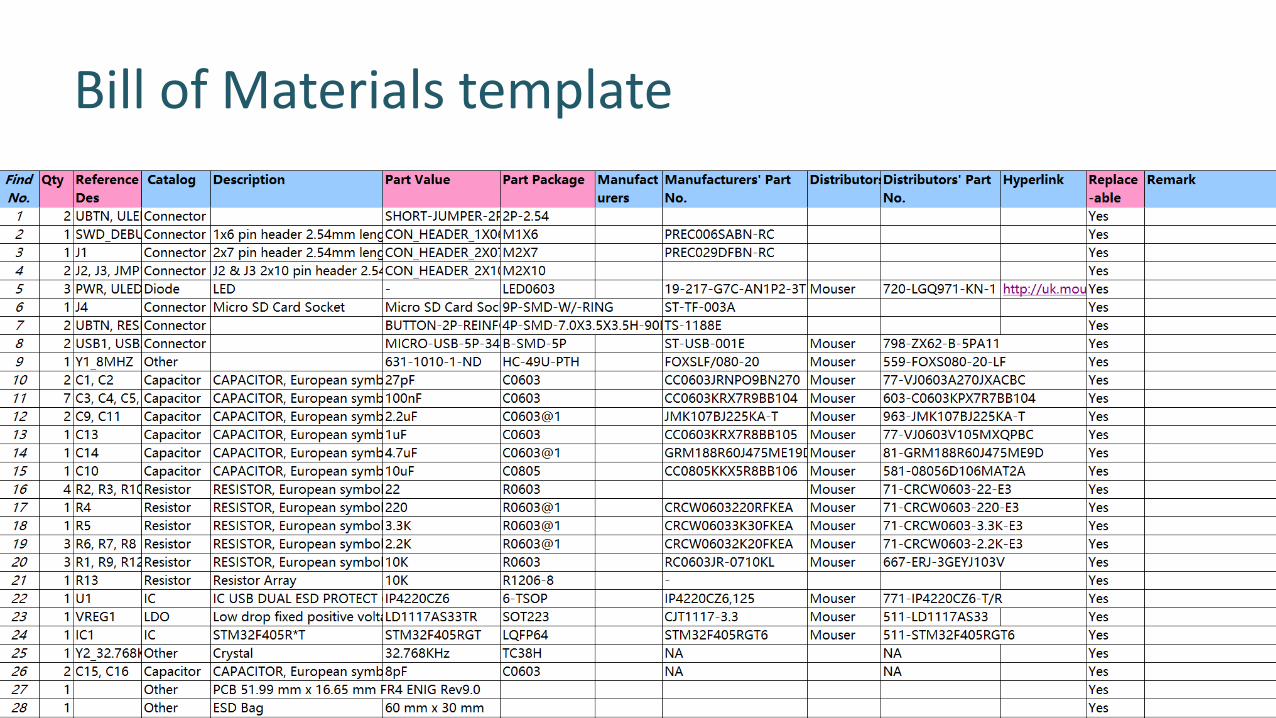
Bill of Materials template
BOM DFM hints
• Don’t assume people knows
• Always have Plan B
• Leave no room for ambiguity
• Consider availability in long run
• Consider lead time, in worst scenario
25p.seeed.cc
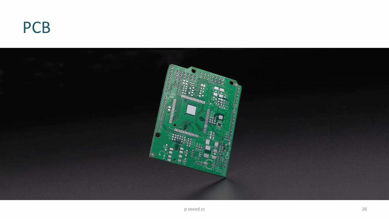
PCB
26p.seeed.cc
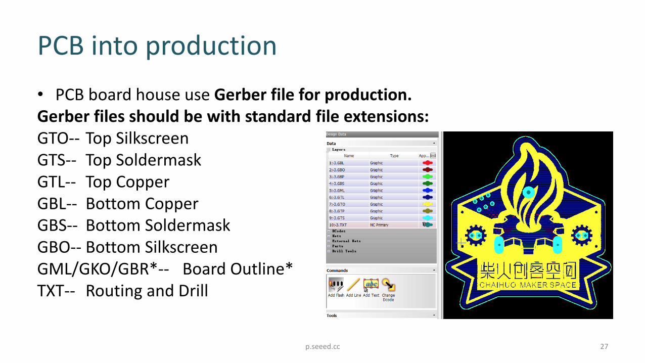
• PCB board house use Gerber file for production. Gerber files should be with standard file extensions:GTO-- Top Silkscreen GTS-- Top SoldermaskGTL-- Top Copper GBL-- Bottom CopperGBS-- Bottom SoldermaskGBO-- Bottom SilkscreenGML/GKO/GBR*-- Board Outline*TXT-- Routing and Drill
PCB into production
27p.seeed.cc

28p.seeed.cc
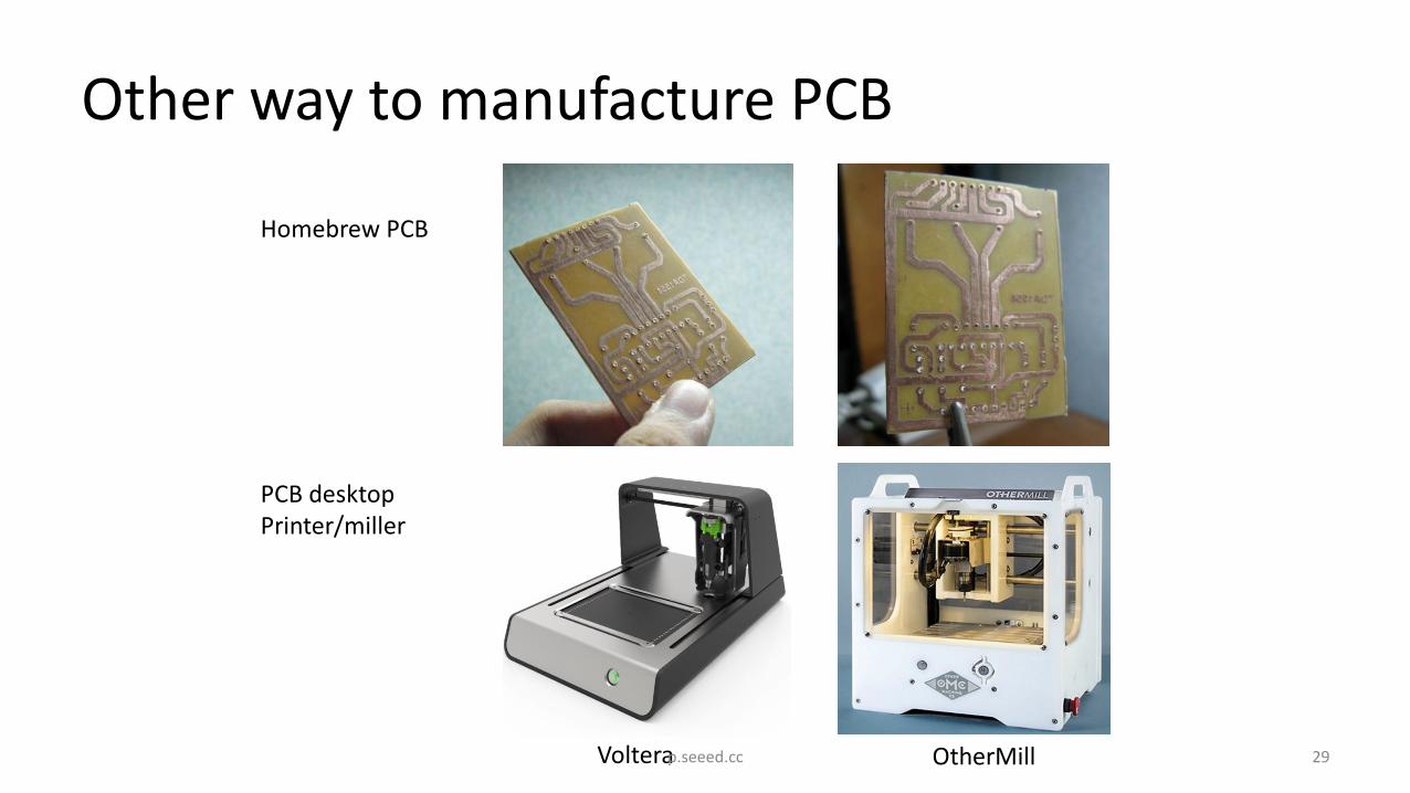
Other way to manufacture PCB
PCB desktopPrinter/miller
Homebrew PCB
Voltera OtherMill 29p.seeed.cc
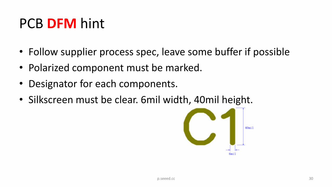
PCB DFM hint
• Follow supplier process spec, leave some buffer if possible
• Polarized component must be marked.
• Designator for each components.
• Silkscreen must be clear. 6mil width, 40mil height.
30p.seeed.cc
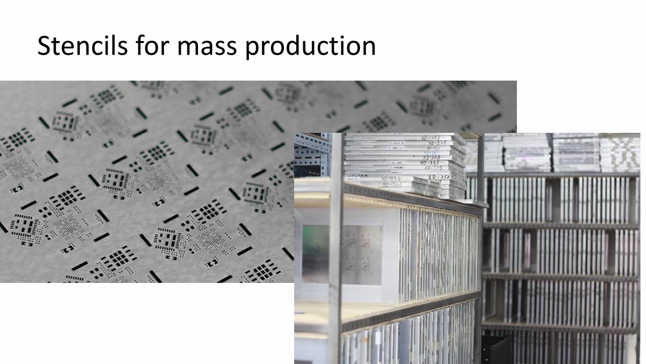
Stencils for mass production
p.seeed.cc 31
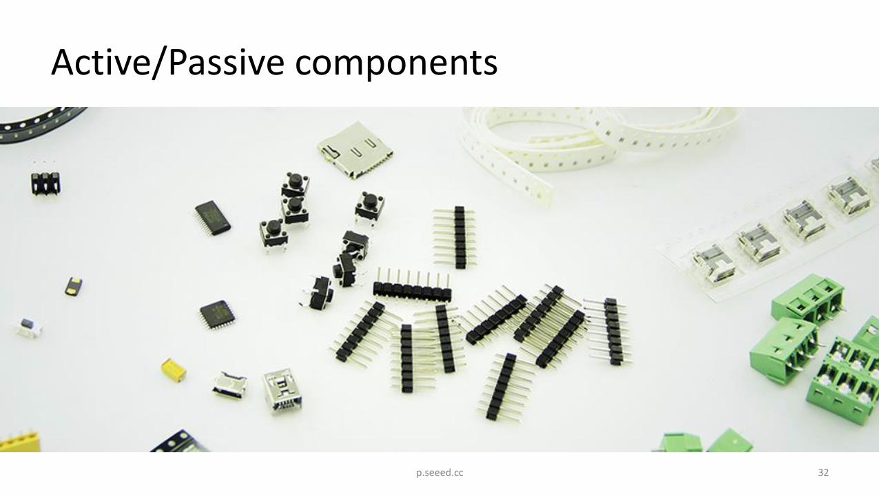
Active/Passive components
32p.seeed.cc
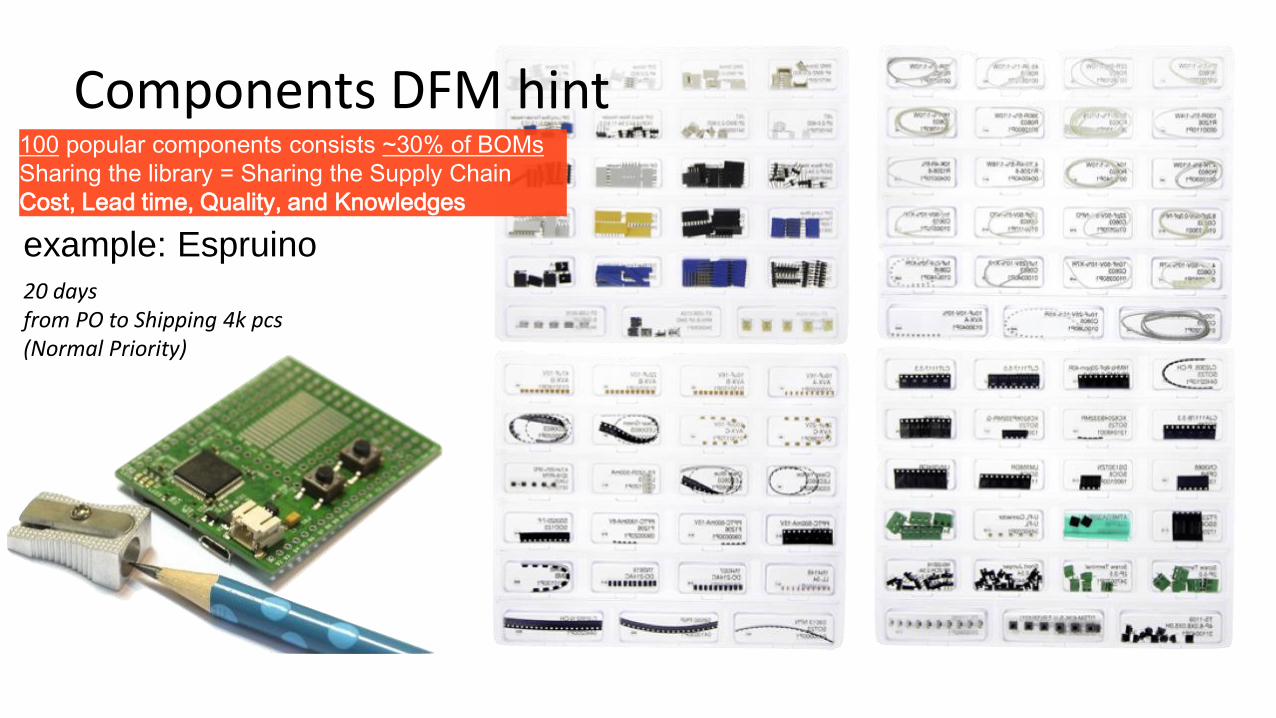
example: Espruino
20 days from PO to Shipping 4k pcs(Normal Priority)
100 popular components consists ~30% of BOMs
Sharing the library = Sharing the Supply Chain
Cost, Lead time, Quality, and Knowledges
Components DFM hint
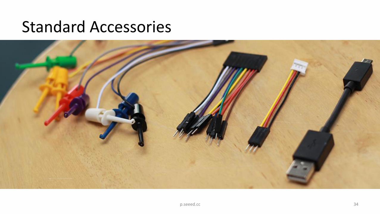
Standard Accessories
34p.seeed.cc
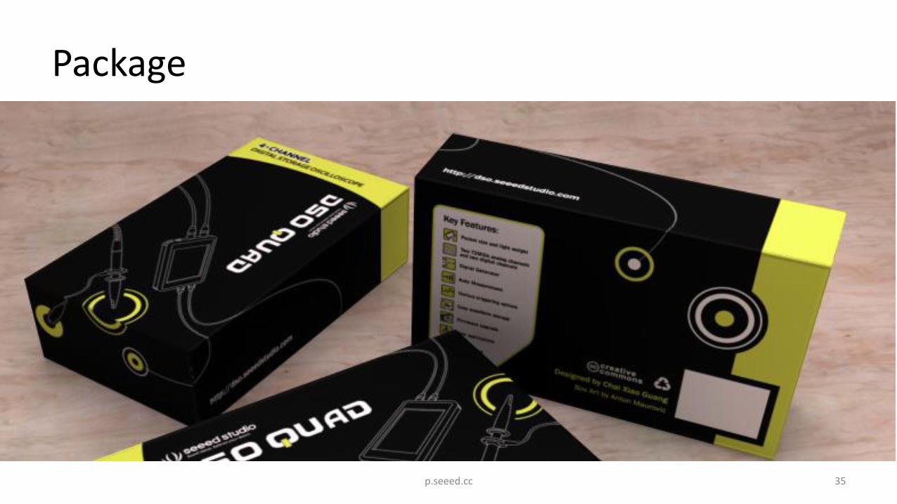
Package
35p.seeed.cc
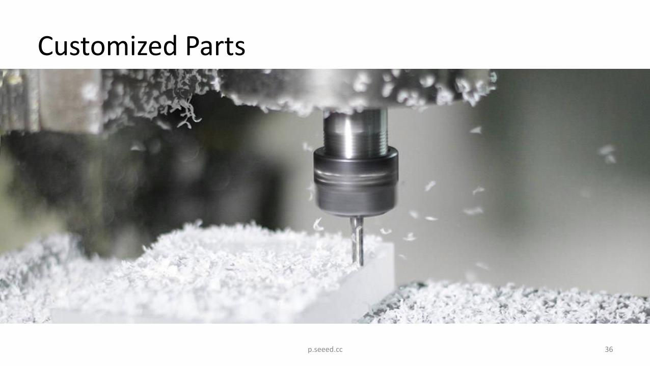
Customized Parts
36p.seeed.cc
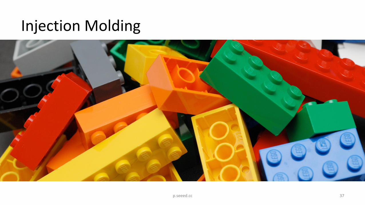
Injection Molding
37p.seeed.cc

38
Chapter 3
Assembly
p.seeed.cc
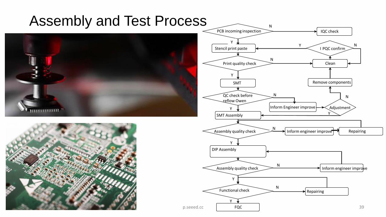
Assembly and Test Process
Y
Y
Y
Stencil print paste
SMT
SMT Assembly
DIP Assembly
PCB incoming inspection
Print quality check
QC check beforereflow Owen
Assembly quality check
Functional check
Assembly quality check
IQC check
Clean
Inform Engineer improve
I PQC confirm
Repairing
Adjustment
Inform engineer improve
Remove components
FQC
Repairing
Y
Y
Y
Y
N
N
N
N
N
N
N
N
Y
Inform engineer improve
39p.seeed.cc
40p.seeed.cc
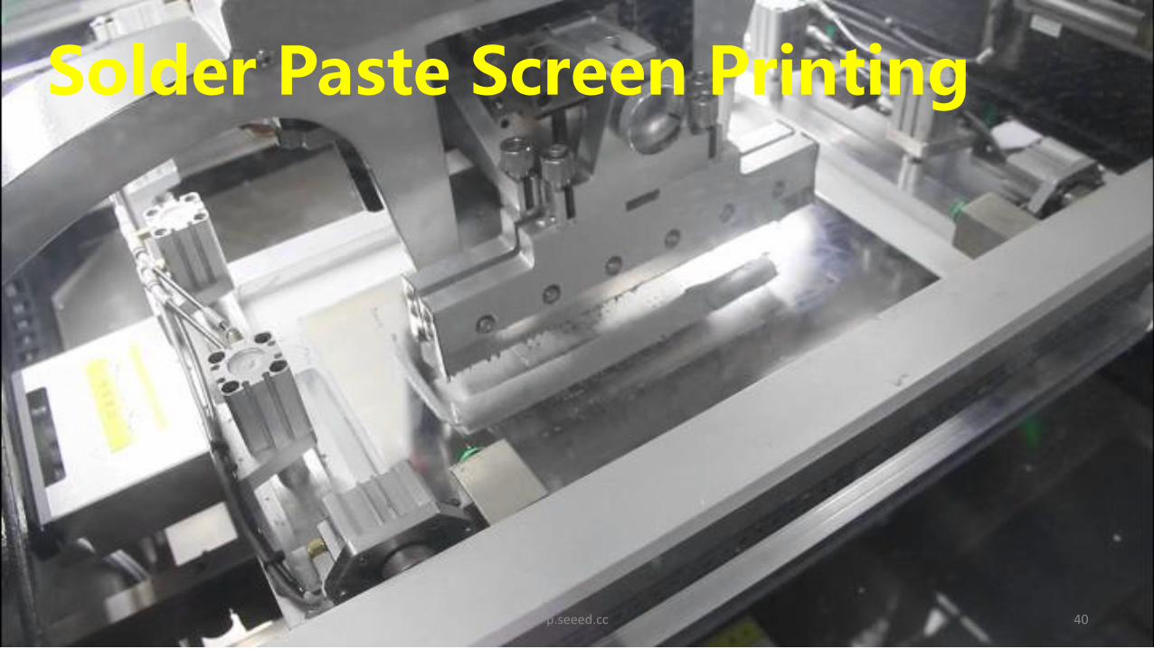
Solder Paste Screen Printing
41p.seeed.cc
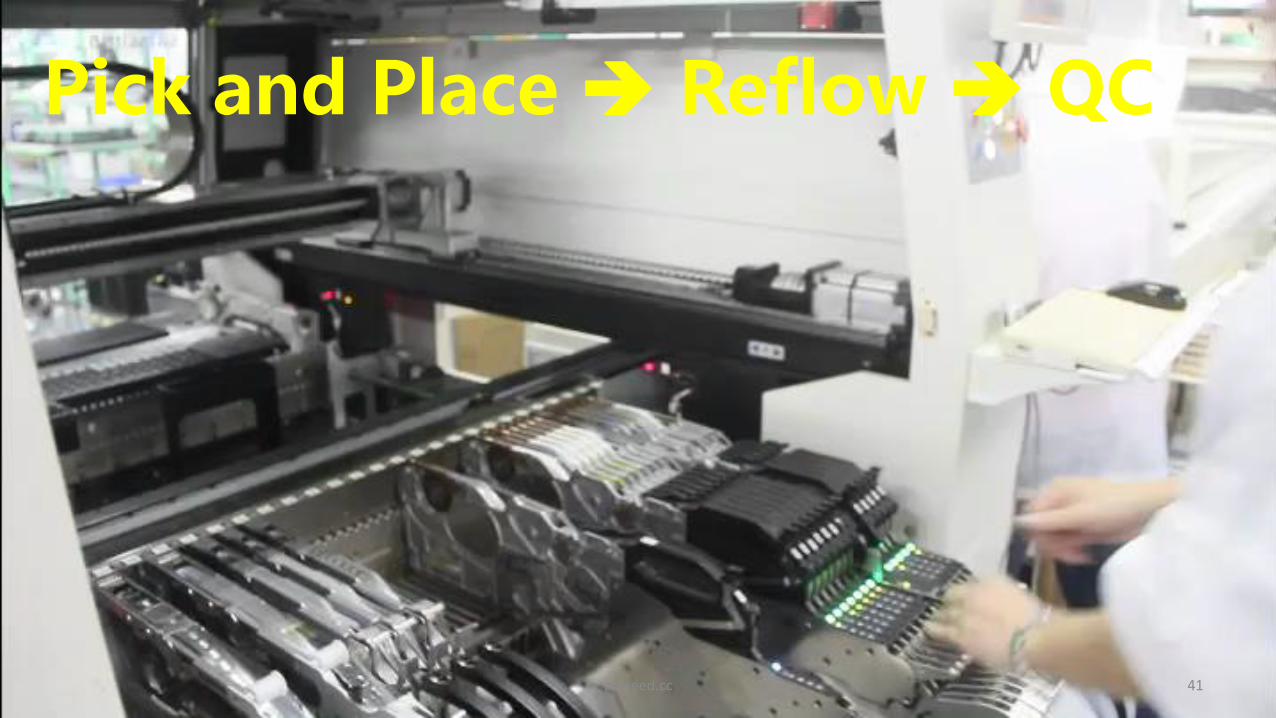
Pick and Place Reflow QC
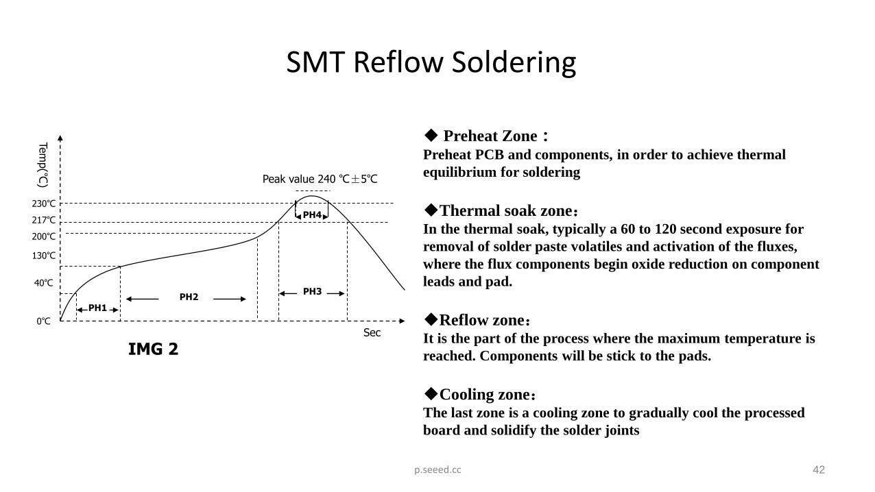
40℃
130℃
200℃
217℃
230℃
0℃
PH1PH2
PH3
PH4
Peak value 240 ℃±5℃
Sec
Tem
p(℃
)
IMG 2
42
SMT Reflow Soldering
p.seeed.cc
Preheat Zone:Preheat PCB and components, in order to achieve thermal
equilibrium for soldering
Thermal soak zone:In the thermal soak, typically a 60 to 120 second exposure for
removal of solder paste volatiles and activation of the fluxes,
where the flux components begin oxide reduction on component
leads and pad.
Reflow zone:It is the part of the process where the maximum temperature is
reached. Components will be stick to the pads.
Cooling zone:The last zone is a cooling zone to gradually cool the processed
board and solidify the solder joints
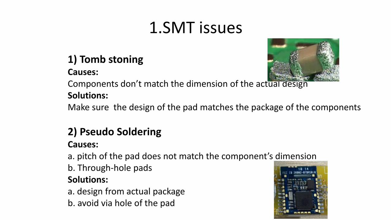
1) Tomb stoningCauses: Components don’t match the dimension of the actual designSolutions:Make sure the design of the pad matches the package of the components
2) Pseudo SolderingCauses: a. pitch of the pad does not match the component’s dimensionb. Through-hole pads Solutions: a. design from actual package b. avoid via hole of the pad
1.SMT issues
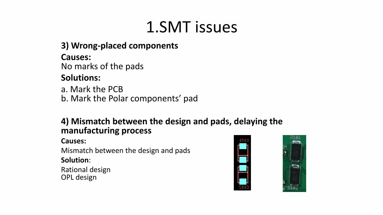
1.SMT issues3) Wrong-placed componentsCauses: No marks of the padsSolutions: a. Mark the PCBb. Mark the Polar components’ pad
4) Mismatch between the design and pads, delaying the manufacturing processCauses:Mismatch between the design and padsSolution:Rational designOPL design
SMT DFM hints
• Compassion for machines
• Align same components in order
• Leave adequate spacing for thermal parts
• Leave enough margin to PCB edge
• Avoid double side placement if possible
45p.seeed.cc
46p.seeed.cc
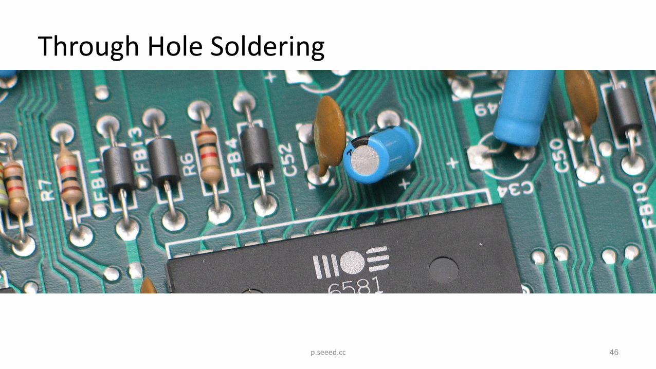
Through Hole Soldering
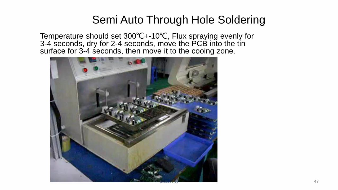
Semi Auto Through Hole Soldering
Temperature should set 300℃+-10℃, Flux spraying evenly for3-4 seconds, dry for 2-4 seconds, move the PCB into the tin surface for 3-4 seconds, then move it to the cooing zone.
47p.seeed.cc
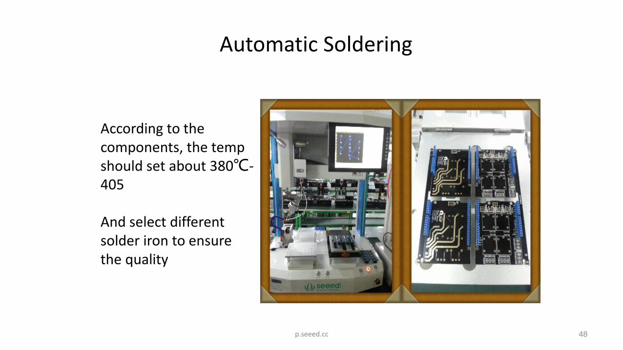
Automatic Soldering
48
According to thecomponents, the tempshould set about 380℃-405
And select differentsolder iron to ensurethe quality
p.seeed.cc
49p.seeed.cc
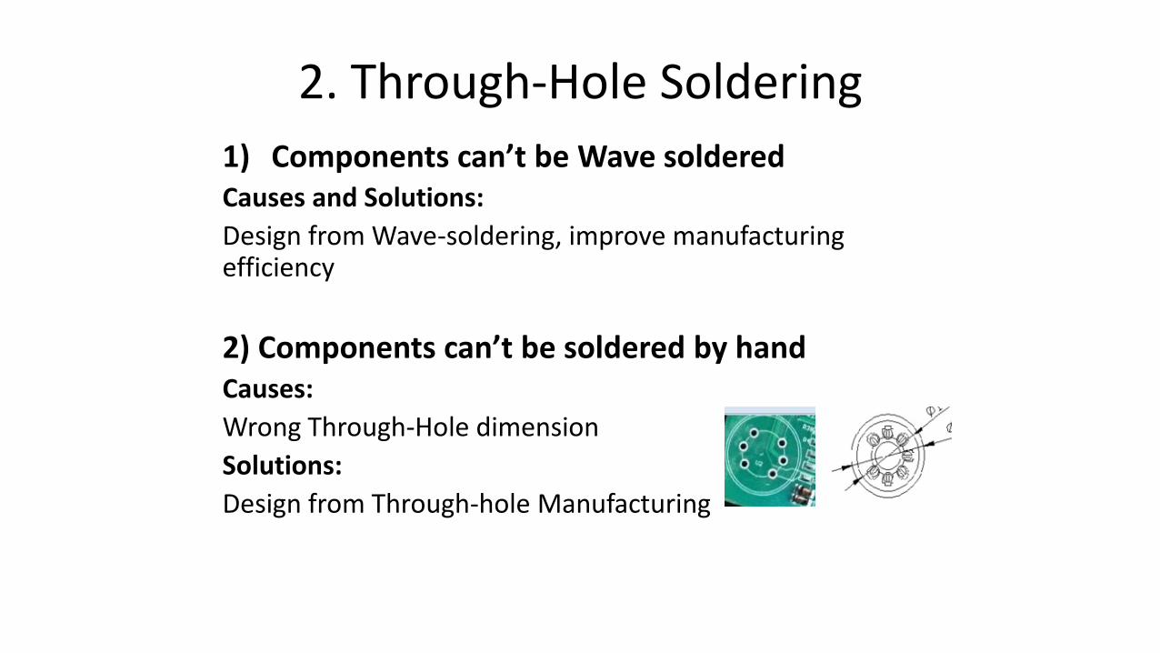
1) Components can’t be Wave soldered Causes and Solutions:
Design from Wave-soldering, improve manufacturing efficiency
2) Components can’t be soldered by handCauses:
Wrong Through-Hole dimension
Solutions:
Design from Through-hole Manufacturing
2. Through-Hole Soldering
2. Through-Hole Soldering
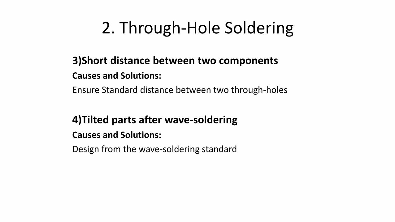
3)Short distance between two components
Causes and Solutions:
Ensure Standard distance between two through-holes
4)Tilted parts after wave-soldering
Causes and Solutions:
Design from the wave-soldering standard
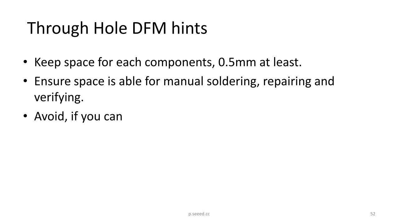
• Keep space for each components, 0.5mm at least.
• Ensure space is able for manual soldering, repairing and verifying.
• Avoid, if you can
Through Hole DFM hints
52p.seeed.cc

53
Chapter 4
Test and Package
p.seeed.cc
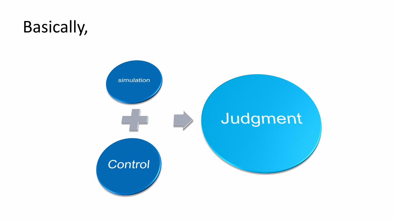
Basically,
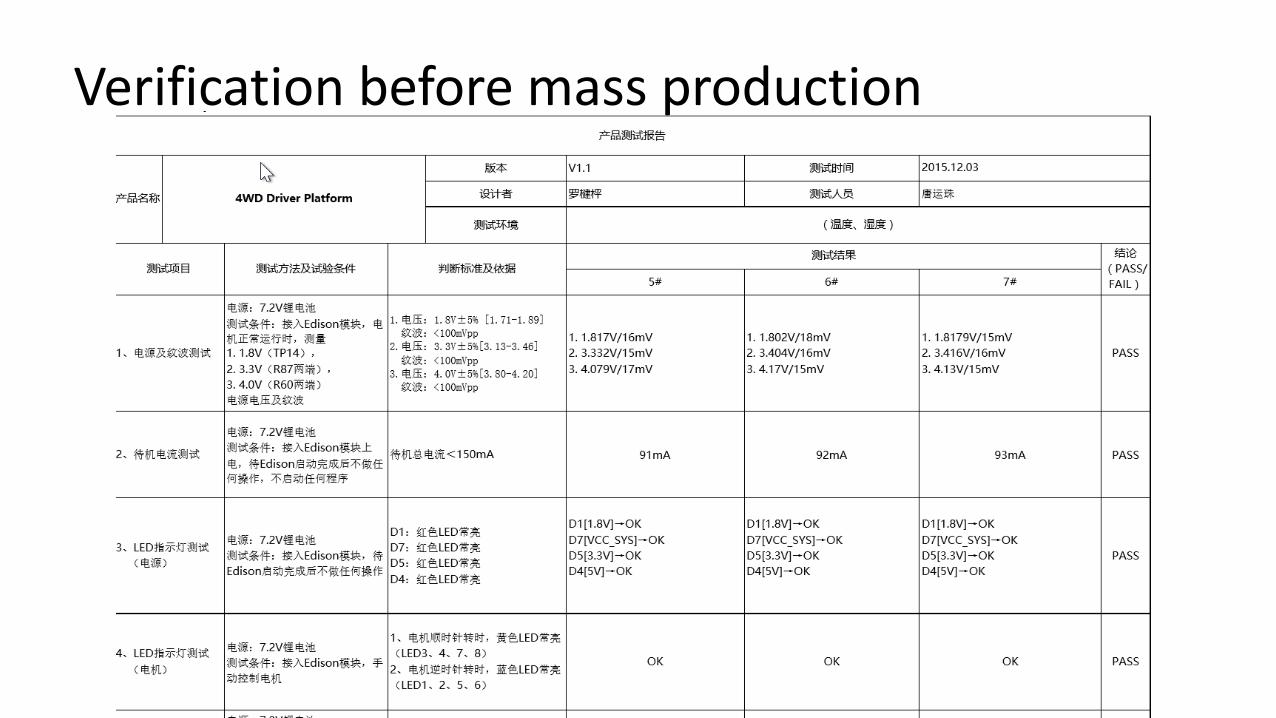
Verification before mass production
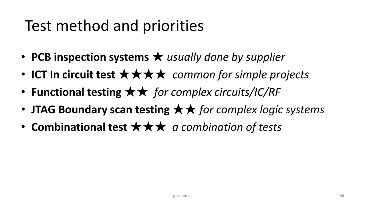
• PCB inspection systems ★ usually done by supplier
• ICT In circuit test ★★★★ common for simple projects
• Functional testing ★★ for complex circuits/IC/RF
• JTAG Boundary scan testing ★★ for complex logic systems
• Combinational test ★★★ a combination of tests
Test method and priorities
56p.seeed.cc
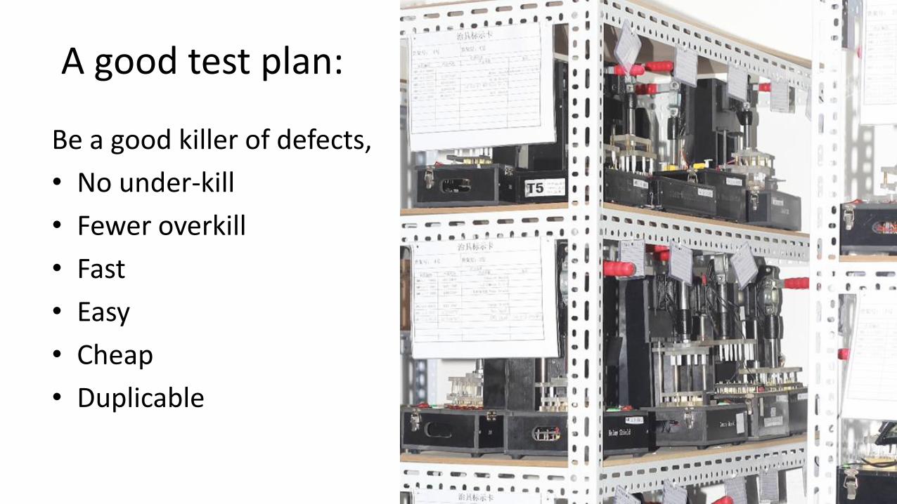
Be a good killer of defects,
• No under-kill
• Fewer overkill
• Fast
• Easy
• Cheap
• Duplicable
A good test plan:
57p.seeed.cc
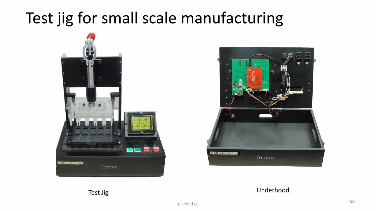
Test jig for small scale manufacturing
p.seeed.cc58
Test Jig Underhood
59p.seeed.cc
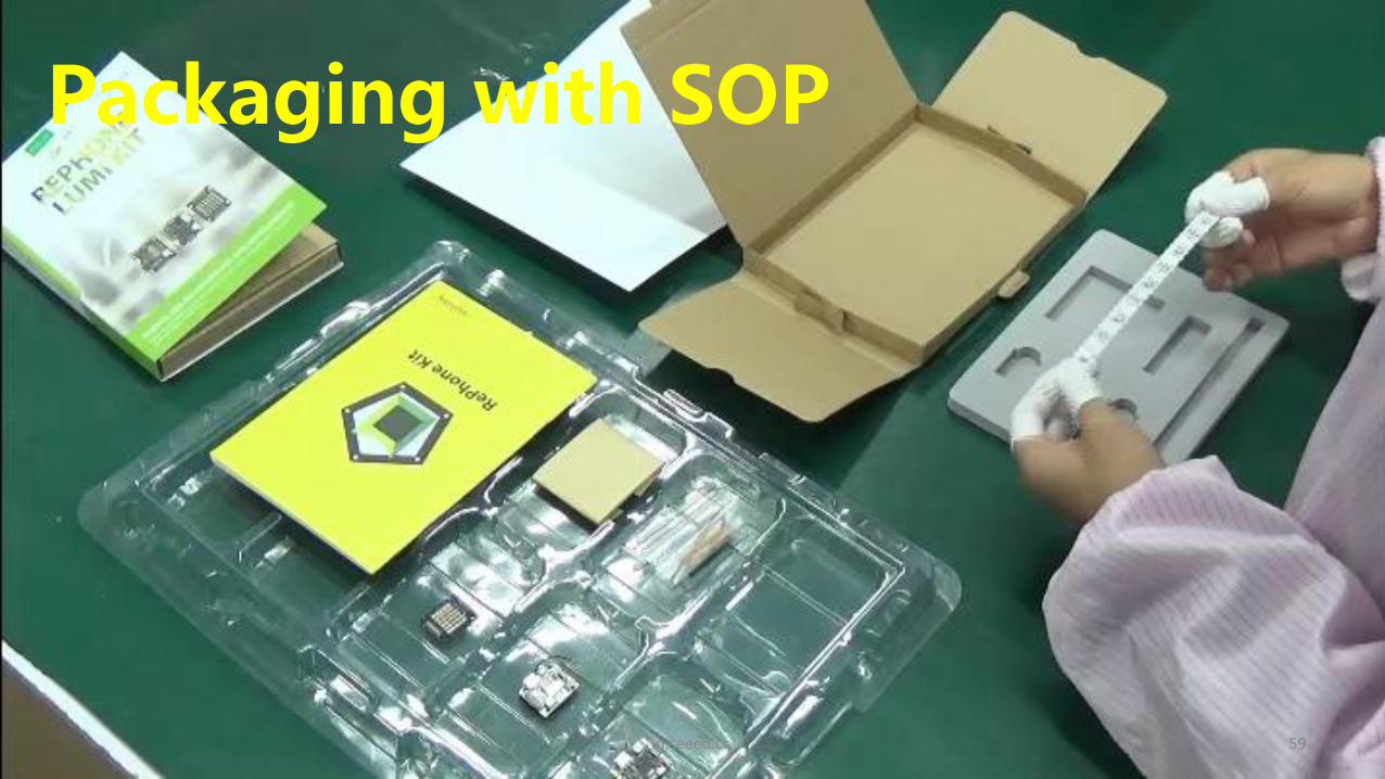
Packaging with SOP
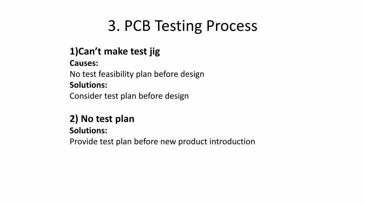
3. PCB Testing Process
1)Can’t make test jigCauses:No test feasibility plan before design Solutions:Consider test plan before design
2) No test plan Solutions:Provide test plan before new product introduction
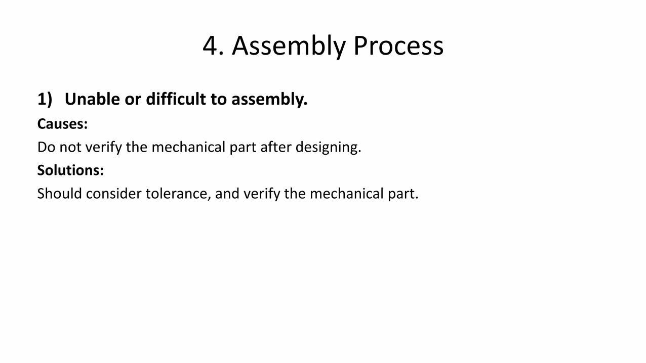
1) Unable or difficult to assembly.
Causes:
Do not verify the mechanical part after designing.
Solutions:
Should consider tolerance, and verify the mechanical part.
4. Assembly Process
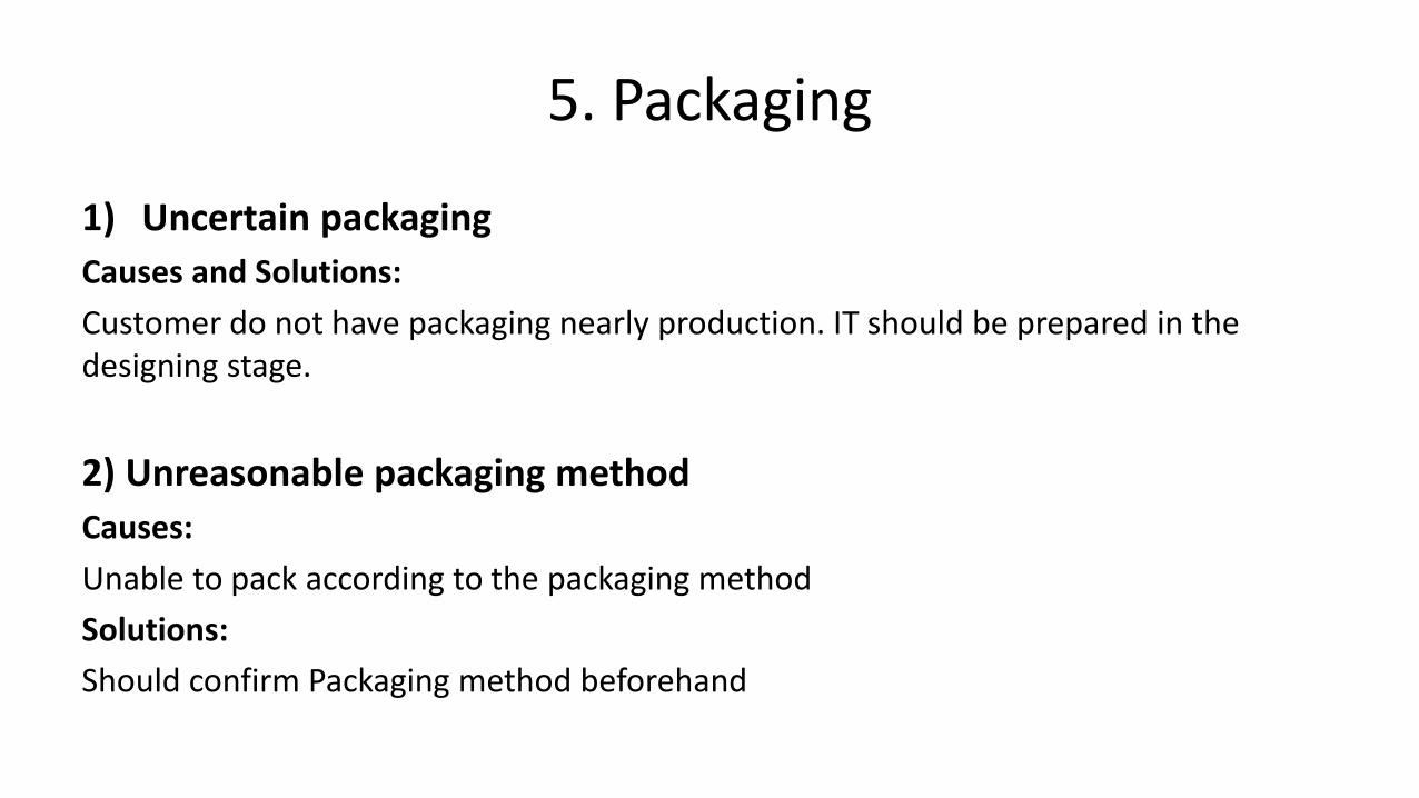
1) Uncertain packaging
Causes and Solutions:
Customer do not have packaging nearly production. IT should be prepared in thedesigning stage.
2) Unreasonable packaging method
Causes:
Unable to pack according to the packaging method
Solutions:
Should confirm Packaging method beforehand
5. Packaging
Assembly and Test hints
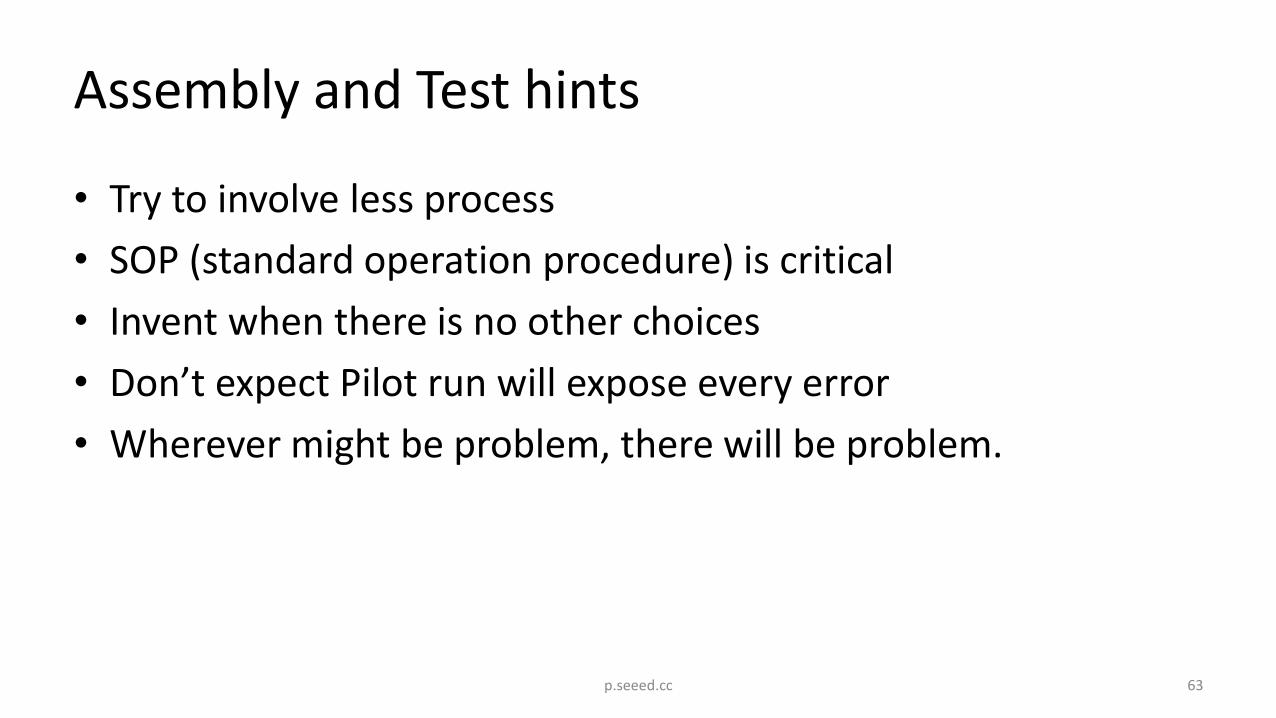
• Try to involve less process
• SOP (standard operation procedure) is critical
• Invent when there is no other choices
• Don’t expect Pilot run will expose every error
• Wherever might be problem, there will be problem.
p.seeed.cc 63

64
Chapter 5
Takeaways
p.seeed.cc
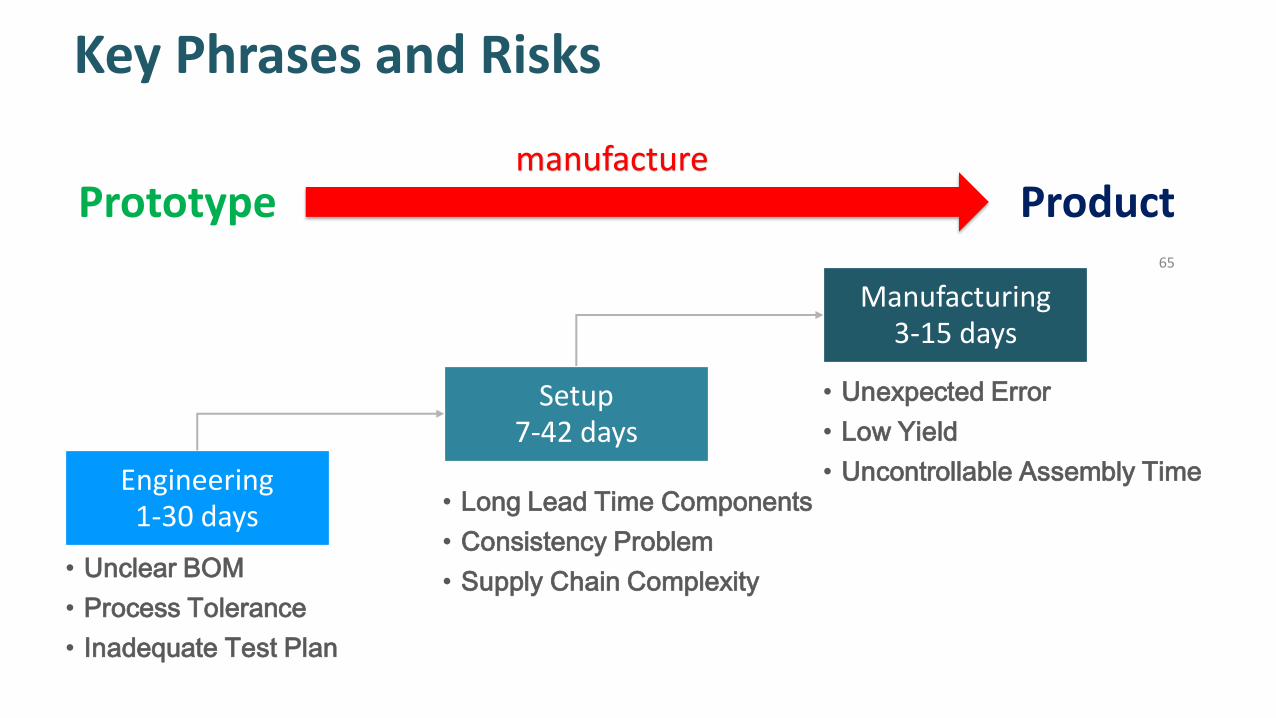
65
Setup7-42 days
Manufacturing3-15 days
Engineering1-30 days
• Unclear BOM
• Process Tolerance
• Inadequate Test Plan
• Long Lead Time Components
• Consistency Problem
• Supply Chain Complexity
• Unexpected Error
• Low Yield
• Uncontrollable Assembly Time
Prototype Productmanufacture
Key Phrases and Risks
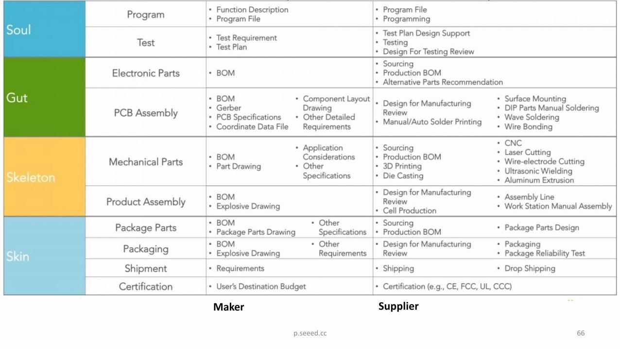
66p.seeed.cc
Maker Supplier
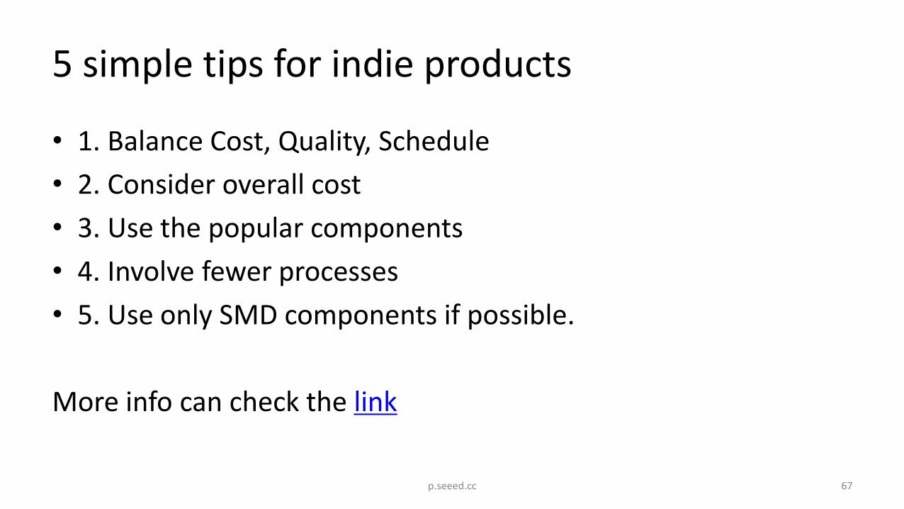
5 simple tips for indie products
• 1. Balance Cost, Quality, Schedule
• 2. Consider overall cost
• 3. Use the popular components
• 4. Involve fewer processes
• 5. Use only SMD components if possible.
More info can check the link
67p.seeed.cc

68
Chapter 6
Practice
p.seeed.cc

Let’s redefine hat
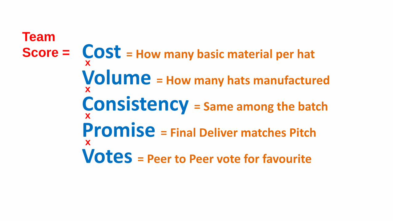
Cost = How many basic material per hat
Volume = How many hats manufactured
Consistency = Same among the batch
Promise = Final Deliver matches Pitch
Votes = Peer to Peer vote for favourite
Team
Score = x
x
x
x
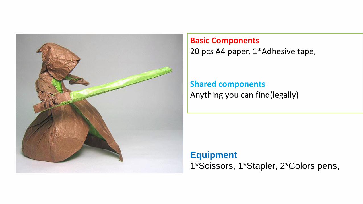
Basic Components20 pcs A4 paper, 1*Adhesive tape,
Shared componentsAnything you can find(legally)
Equipment
1*Scissors, 1*Stapler, 2*Colors pens,
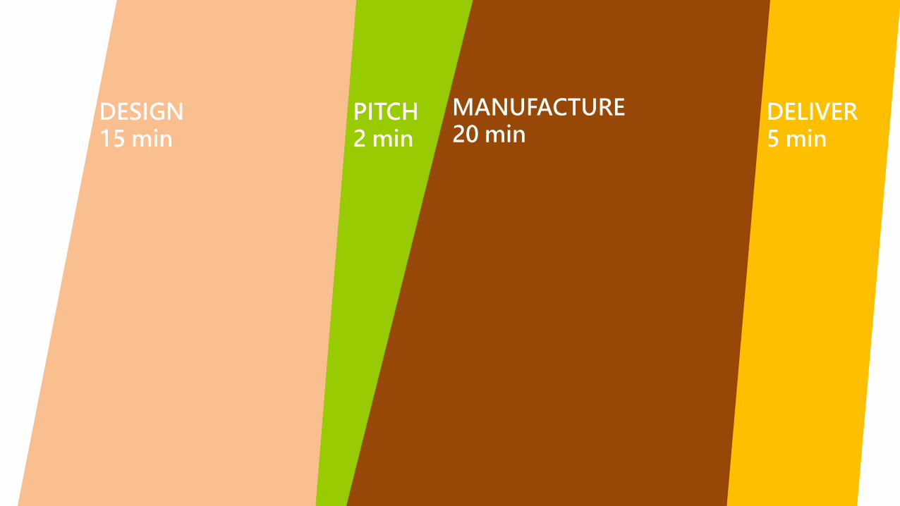
Design – Pitch – Manufacture – Deliver
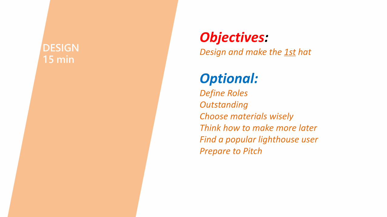
DESIGN15 min
PITCH2 min
MANUFACTURE20 min
DELIVER5 min
DESIGN15 min
Objectives:Design and make the 1st hat
Optional:Define RolesOutstandingChoose materials wiselyThink how to make more laterFind a popular lighthouse userPrepare to Pitch
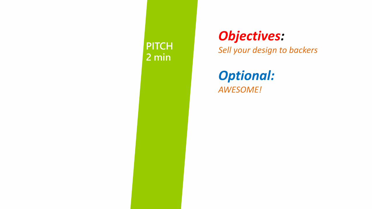
PITCH2 min
Objectives:Sell your design to backers
Optional:AWESOME!
MANUFACTURE20 min
Objectives:Manufacture more hats!
Optional:Collect enough materialPrepare a operation procedureOptimize the processApply Quality Control
Objectives:Show us the results!
Optional:A moving storyImprovement (downgrade) appliedShare your hints
DELIVER5 min

A free fusion PCB coupon for the submitterA free fusion PCBA coupon for the winner
Share your result photo/thoughts via twitter @seeedstudio #fusion, to win

Diving by sport in touch UK, from Pinterest
Good Luck
To the mass
78p.seeed.cc
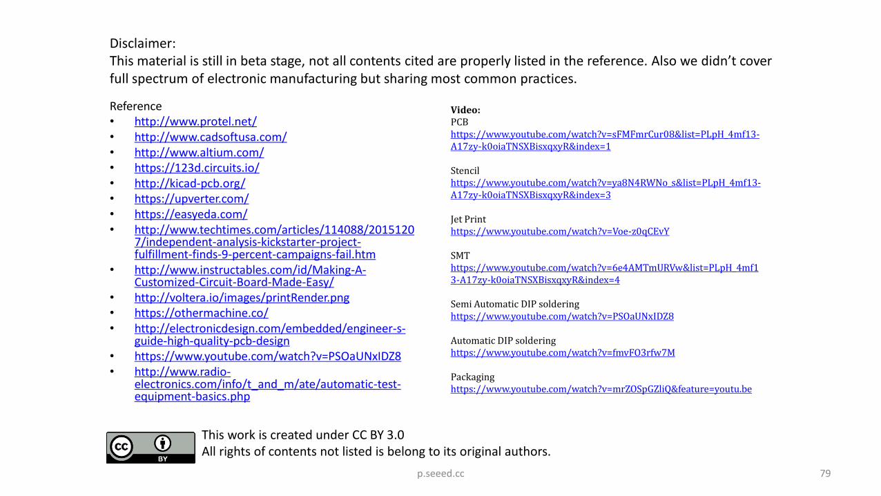
This work is created under CC BY 3.0All rights of contents not listed is belong to its original authors.
79p.seeed.cc
Disclaimer:This material is still in beta stage, not all contents cited are properly listed in the reference. Also we didn’t cover full spectrum of electronic manufacturing but sharing most common practices.
Video:PCBhttps://www.youtube.com/watch?v=sFMFmrCur08&list=PLpH_4mf13-A17zy-k0oiaTNSXBisxqxyR&index=1
Stencilhttps://www.youtube.com/watch?v=ya8N4RWNo_s&list=PLpH_4mf13-A17zy-k0oiaTNSXBisxqxyR&index=3
Jet Printhttps://www.youtube.com/watch?v=Voe-z0qCEvY
SMThttps://www.youtube.com/watch?v=6e4AMTmURVw&list=PLpH_4mf13-A17zy-k0oiaTNSXBisxqxyR&index=4
Semi Automatic DIP solderinghttps://www.youtube.com/watch?v=PSOaUNxIDZ8
Automatic DIP solderinghttps://www.youtube.com/watch?v=fmvFO3rfw7M
Packaginghttps://www.youtube.com/watch?v=mrZOSpGZliQ&feature=youtu.be
Reference• http://www.protel.net/• http://www.cadsoftusa.com/• http://www.altium.com/• https://123d.circuits.io/• http://kicad-pcb.org/• https://upverter.com/• https://easyeda.com/• http://www.techtimes.com/articles/114088/2015120
7/independent-analysis-kickstarter-project-fulfillment-finds-9-percent-campaigns-fail.htm
• http://www.instructables.com/id/Making-A-Customized-Circuit-Board-Made-Easy/
• http://voltera.io/images/printRender.png• https://othermachine.co/• http://electronicdesign.com/embedded/engineer-s-
guide-high-quality-pcb-design• https://www.youtube.com/watch?v=PSOaUNxIDZ8• http://www.radio-
electronics.com/info/t_and_m/ate/automatic-test-equipment-basics.php