electronic mechanical coupling in graphene from in situ ... › download › pdf › 4888693.pdf ·...
TRANSCRIPT
Published: February 10, 2011
r 2011 American Chemical Society 1241 dx.doi.org/10.1021/nl104227t |Nano Lett. 2011, 11, 1241–1246
LETTER
pubs.acs.org/NanoLett
Electronic-Mechanical Coupling in Graphene from in situNanoindentation Experiments and Multiscale Atomistic SimulationsMingyuan Huang,*,† Tod A. Pascal,‡,§ Hyungjun Kim,‡,§ William A. Goddard, III,‡,§ and Julia R. Greer†
†Division of Engineering and Applied Science, California Institute of Technology, 1200 East California Boulevard,MC 309-81, Pasadena,California 91125-8100, United States‡Center for Materials Simulations and Design, Graduate School of EEWS, Korea Advanced Institute of Science and Technology,Daejeon, Korea§Materials and Process Simulation Center, California Institute of Technology, 1200 East California Boulevard, MC 309-81, Pasadena,California 91125-8100, United States
bS Supporting Information
ABSTRACT:
We present the in situ nanoindentation experiments performed on suspended graphene devices to introduce homogeneous tensilestrain, while simultaneously carrying out electrical measurements.We find that the electrical resistance shows only amarginal changeeven under severe strain, and the electronic transport measurement confirms that there is no band gap opening for graphene undermoderate uniform strain, which is consistent with our results from the first-principles informed molecular dynamics simulation.
KEYWORDS: Graphene, nanoindentation, strain, electronic properties
Graphene, a truly two-dimensional gapless semiconductor,1,2
recently deemed strongest material ever measured, cansustain very high, up to 25%, in-plane tensile elastic strains.3
Straining graphene to such a significant elongation is likely toshift its electronic band structure and elicit intriguing electronicproperties, resulting in notable electrical-mechanical coupling.Several recent theoretical-only studies on strained graphenepredict that strain can shift the Dirac cones, reduce the Fermivelocity, introduce a pseudomagnetic field, and be used toengineer the electronic structure.4-10 Moreover, theory alsosuggests that uniaxial strains below a very high value of ∼23%would not be capable of opening a band gap in graphene,5 whichmay be crucial for the utilization of this material in futureelectronic devices. On the experimental side, optical measure-ments revealed that strain induces a disruption of graphene’ssymmetry and a shift of the Dirac cone,11-13 while scanningtunneling microscopy (STM) studies conveyed the presence of apseudomagnetic field in highly strained graphene nanobubblesystems.14 However, no direct experiments on electrical mea-surements of strained graphene have yet been reported. Here, wepresent the results of in situ investigation of electrical-mechan-ical coupling in graphene-based devices.
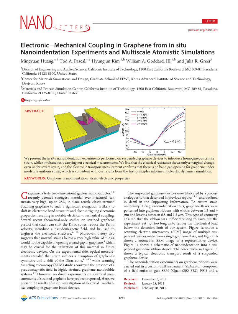
The suspended graphene devices were fabricated by a processanalogous to that described in previous reports15,16 and outlinedin detail in the Supporting Information. To ensure strainuniformity during nanoindentation tests, graphene flakes werepatterned into graphene ribbons with widths between 1.5 and 4μm and lengths between 0.8 and 1.2 μm. This type of geometryensured that the ribbon was sufficiently long to carry out theexperiment yet not too long as to render the mechanical loadbelow the detection limit of our system. Figure 1a shows ascanning electron microscopy (SEM) image of multiple sus-pended devices made from a single graphene flake, and Figure 1bshows a zoomed-in SEM image of a representative device.Figure 1c shows a schematic of nanoindentation into a sus-pended graphene ribbon device. The black curve in Figure 1dshows a typical electronic transport result of a suspendedgraphene device.
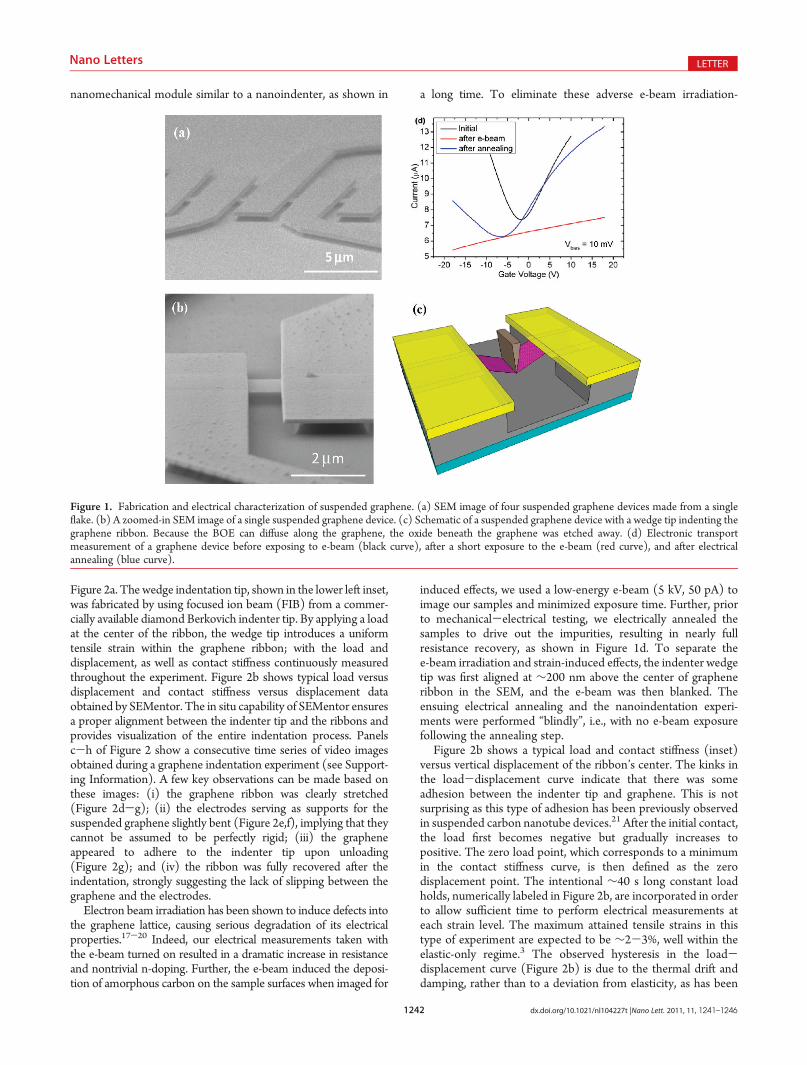
The nanoindentation experiments on graphene ribbons werecarried out in a custom-built instrument, SEMentor, composedof a field-emission gun SEM (Quanta200 FEG, FEI) and a
Received: December 3, 2010Revised: January 25, 2011
1242 dx.doi.org/10.1021/nl104227t |Nano Lett. 2011, 11, 1241–1246
Nano Letters LETTER
nanomechanical module similar to a nanoindenter, as shown in
Figure 2a. The wedge indentation tip, shown in the lower left inset,was fabricated by using focused ion beam (FIB) from a commer-cially available diamond Berkovich indenter tip. By applying a loadat the center of the ribbon, the wedge tip introduces a uniformtensile strain within the graphene ribbon; with the load anddisplacement, as well as contact stiffness continuously measuredthroughout the experiment. Figure 2b shows typical load versusdisplacement and contact stiffness versus displacement dataobtained by SEMentor. The in situ capability of SEMentor ensuresa proper alignment between the indenter tip and the ribbons andprovides visualization of the entire indentation process. Panelsc-h of Figure 2 show a consecutive time series of video imagesobtained during a graphene indentation experiment (see Support-ing Information). A few key observations can be made based onthese images: (i) the graphene ribbon was clearly stretched(Figure 2d-g); (ii) the electrodes serving as supports for thesuspended graphene slightly bent (Figure 2e,f), implying that theycannot be assumed to be perfectly rigid; (iii) the grapheneappeared to adhere to the indenter tip upon unloading(Figure 2g); and (iv) the ribbon was fully recovered after theindentation, strongly suggesting the lack of slipping between thegraphene and the electrodes.
Electron beam irradiation has been shown to induce defects intothe graphene lattice, causing serious degradation of its electricalproperties.17-20 Indeed, our electrical measurements taken withthe e-beam turned on resulted in a dramatic increase in resistanceand nontrivial n-doping. Further, the e-beam induced the deposi-tion of amorphous carbon on the sample surfaces when imaged for
a long time. To eliminate these adverse e-beam irradiation-
induced effects, we used a low-energy e-beam (5 kV, 50 pA) toimage our samples and minimized exposure time. Further, priorto mechanical-electrical testing, we electrically annealed thesamples to drive out the impurities, resulting in nearly fullresistance recovery, as shown in Figure 1d. To separate thee-beam irradiation and strain-induced effects, the indenter wedgetip was first aligned at ∼200 nm above the center of grapheneribbon in the SEM, and the e-beam was then blanked. Theensuing electrical annealing and the nanoindentation experi-ments were performed “blindly”, i.e., with no e-beam exposurefollowing the annealing step.
Figure 2b shows a typical load and contact stiffness (inset)versus vertical displacement of the ribbon’s center. The kinks inthe load-displacement curve indicate that there was someadhesion between the indenter tip and graphene. This is notsurprising as this type of adhesion has been previously observedin suspended carbon nanotube devices.21 After the initial contact,the load first becomes negative but gradually increases topositive. The zero load point, which corresponds to a minimumin the contact stiffness curve, is then defined as the zerodisplacement point. The intentional ∼40 s long constant loadholds, numerically labeled in Figure 2b, are incorporated in orderto allow sufficient time to perform electrical measurements ateach strain level. The maximum attained tensile strains in thistype of experiment are expected to be ∼2-3%, well within theelastic-only regime.3 The observed hysteresis in the load-displacement curve (Figure 2b) is due to the thermal drift anddamping, rather than to a deviation from elasticity, as has been
Figure 1. Fabrication and electrical characterization of suspended graphene. (a) SEM image of four suspended graphene devices made from a singleflake. (b) A zoomed-in SEM image of a single suspended graphene device. (c) Schematic of a suspended graphene device with a wedge tip indenting thegraphene ribbon. Because the BOE can diffuse along the graphene, the oxide beneath the graphene was etched away. (d) Electronic transportmeasurement of a graphene device before exposing to e-beam (black curve), after a short exposure to the e-beam (red curve), and after electricalannealing (blue curve).

1243 dx.doi.org/10.1021/nl104227t |Nano Lett. 2011, 11, 1241–1246
Nano Letters LETTER
observed previously on suspended thin film metallic samples.22
The 100% reversibility of the stiffness-displacement data indi-cates that the mechanical deformation is indeed elastic and thatthere was no slippage between the graphene and the electrodes.
According to a suspended bridge model developed by Herbertet al.,22 the elastic deflection h of the center point in response to aline load P across the center of the graphene ribbon can beexpressed as
P ¼ 8wE2D
l3h3 þ 8wσ2D
lh ð1Þ
where w and l are the width and the length of the grapheneribbon, E2D is the two-dimensional Young’s modulus, and σ2D isthe residual tension in the as-fabricated ribbon. While thisequation was found to describe the deflection of suspendedmetallic films well, the model’s fundamental assumption is thatthe effects of the bending moments are negligible, so that onlystretching is dominating the deformation. We find this assump-tion to be valid for our graphene analysis since its thickness is 4
orders of magnitude smaller than its length. Another assumptionof this model is that the support electrodes are infinitely stiff.However, as can be clearly seen in Figure 2e, the electrodes bentduring the deformation. To address this issue, we used finiteelement method (ABAQUS) to simulate the bending of theelectrodes and to calculate this additional bending stiffness (seeFigure S1, Supporting Information). The additional displace-ment due to this bending is then subtracted from the overalldeflection measured by the instrument to obtain the true loadversus displacement relationship for the graphene ribbon, asshown in Figure 2b. The purple line here is the fit of the loadingdata, based on eq 1, with E2D and σ2D extrapolated from the fitand with the data collected from 10 high-quality samples. Themean extrapolated Young’s modulus is E2D = 335 ( 20 N/m, avalue very close to that reported in other works.3 This valuecorresponds to Young’s modulus of E = 1 TPa for bulk graphite,which also agrees well with the experimental result for the in-plane Young’s modulus in graphite.23 We find that the initial
Figure 2. Experimental setup and mechanical testing results. (a) The in situ mechanical testing setup, SEMentor, is comprised of a field-emission SEM(Quanta200 FEG, FEI) and the DCM module of Agilent nanoindenter.25,26 A custom fabricated wedge tip (inset in bottom left) and the wire-bondeddevice (inset in top right) are shown in the middle picture. The wires from the sample holder are connected to a Keithley source meter to perform theelectrical measurements. (b) A typical load-displacement curve obtained from nanoindentation shows hysteresis due to thermal drift. The attaching anddetaching of the indenter tip from graphene ribbons show a jump in the load due to the adhesion. The numerically labeled constant-load holds are used toperform the electrical measurements. The inset shows the harmonic contact stiffness vs displacement with nearly identical curves during loading andunloading. (c-h) A progressive time series of images taken from a single video taken during nanoindentation.

1244 dx.doi.org/10.1021/nl104227t |Nano Lett. 2011, 11, 1241–1246
Nano Letters LETTER
tension σ2D ranges from 0.08 to 2.4 N/m, also in reasonableagreement with previous reports.3
To probe the electromechanical response of graphene, wemeasured the conductance while indenting the graphene ribbon.Figure 3a shows the I-V characteristics under low bias condi-tions, which were taken during the holds shown in Figure 2b. Thestrain ε in graphene during the holds is ε = 2h2/l2. Interestingly,no significant change in the conductance was observed up to thestrains of 1%, indicating the lack of a noticeable change in theband structure of uniaxially strained graphene. On the basis of the
zoomed-in I-V curves, the conductance appears to decrease by∼2% with 1% strain. In this study, five different samples weremeasured, and the relative change in resistance, extracted bylinear fitting of the I-V curves, was found to be proportional tostrain, as shown in Figure 3b. The gauge factor extracted fromthese curves was 1.9.
To further investigate the band structure of graphene understrain, the electronic transport was measured by taking the highlydoped Si substrate as the back gate. Figure 3c shows theconductance as a function of gate voltage Vg for different strains.We find that our graphene ribbons can sustain up to 20 Vwithoutcollapse. In addition to the load applied by the nanoindenter, theback gate can also electrostatically introduce attractive force intographene ribbons. This force can be estimated as15
Fele ¼ ε0ε2lw
2ðd0 þ εd1Þ2Vg
2 ð2Þ
where d0 = 100 and d1 = 200 nm are the thicknesses of theremaining and etched SiO2. For the typical size of our samples,this electrostatic force is estimated to be∼1� 10-7 N for 20 V,which is 1 order of magnitude lower than the load applied by thenanoindenter, and therefore, can be neglected during subsequentcalculations.
Unlike the I-V measurements, the transport in the gatedgraphene ribbons shows a significant change during straining, asshown in Figure 3c. On the basis of the device geometry, thischange could be due to the increased capacitance, as thegraphene is brought closer to the back gate. As shown inFigure 3c, the minimum conductance of graphene does notchange significantly during the indentation, indicating that theelectronic properties are likely unaffected. All curves in Figure 3ccross atVg = 0, further corroborating that the electrical propertiesare unchanged. As the indenter tip pushes the graphene ribbontoward the back gate, the gate capacitance increases, therebyimproving the gating efficiency, which is likely what we areobserving. The relative change in the gate capacitance can beestimated by monitoring the conductance versus strain slopechanges (inset in Figure 3c). This change can also be calculatedfrom the displacement of the indenter (see Supporting In-formation), shown by the red points in the inset of Figure 3c.Since the calculated values are very close to the experiment data,it is likely that the observed changes in the electronic transport asa function of strain are due to the varying gate capacitance andnot to an alteration in the band structure.
To improve our understanding of the mechanical deformationof graphene at the atomic level, we used extensive moleculardynamics simulations to quantify the effect of indentation on thelocal carbon lattice structure. Since the results of such simulationsdepend critically on the interaction potential and, in particular,on the accuracy of the in-plane phonon modes, we based oursimulations on the QMFF-Cx force field24 validated to reproducethe mechanical and thermodynamic properties of graphite. Theforce field was determined from first principles quantum me-chanics (QM) without empirical parameters that would bias ittoward any particular set of experimental conditions. This last pointis critical, as it allows for the direct application of the force field toother graphitic materials, under various thermodynamic conditions.We test the applicability of QMFF-Cx for graphite by first calculat-ing the mechanical properties at 0 K. We find that the Young’smodulus (1092.7 GPa) and in-plane bulk compressibilities (0.023
Figure 3. Electrical measurements of uniaxially strained graphene:(a) I-V measurement of strained graphene; (b) relative change ofresistance as function of strain; (c) electronic transport measurement ofstrained graphene. The inset shows the relative change of the gatecapacitance from the experiment data (red) and a calculation (blue) as afunction of strain.
1245 dx.doi.org/10.1021/nl104227t |Nano Lett. 2011, 11, 1241–1246
Nano Letters LETTER
1/GPa) are in good agreement with experiments (1020 ( 30GPa and 0.026 1/GPa, respectively).
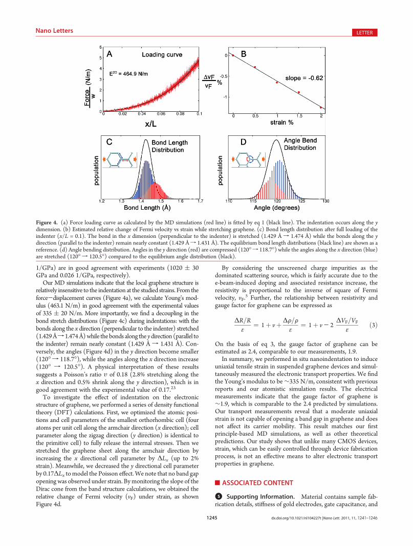
Our MD simulations indicate that the local graphene structure isrelatively insensitive to the indentation at the studied strains. From theforce-displacement curves (Figure 4a), we calculate Young’s mod-ulus (463.1 N/m) in good agreement with the experimental valuesof 335 ( 20 N/m. More importantly, we find a decoupling in thebond stretch distributions (Figure 4c) during indentations: with thebonds along the x direction (perpendicular to the indenter) stretched(1.429Åf1.474Å)while thebonds along the ydirection (parallel tothe indenter) remain nearly constant (1.429 Å f 1.431 Å). Con-versely, the angles (Figure 4d) in the y direction become smaller(120�f 118.7�), while the angles along the x direction increase(120� f 120.5�). A physical interpretation of these resultssuggests a Poisson’s ratio υ of 0.18 (2.8% stretching along thex direction and 0.5% shrink along the y direction), which is ingood agreement with the experimental value of 0.17.23
To investigate the effect of indentation on the electronicstructure of graphene, we performed a series of density functionaltheory (DFT) calculations. First, we optimized the atomic posi-tions and cell parameters of the smallest orthorhombic cell (fouratoms per unit cell along the armchair direction (x direction); cellparameter along the zigzag direction (y direction) is identical tothe primitive cell) to fully release the internal stresses. Then westretched the graphene sheet along the armchair direction byincreasing the x directional cell parameter by ΔLx (up to 2%strain). Meanwhile, we decreased the y directional cell parameterby 0.17ΔLx tomodel the Poisson effect. We note that no band gapopening was observed under strain. Bymonitoring the slope of theDirac cone from the band structure calculations, we obtained therelative change of Fermi velocity (vF) under strain, as shownFigure 4d.
By considering the unscreened charge impurities as thedominated scattering source, which is fairly accurate due to thee-beam-induced doping and associated resistance increase, theresistivity is proportional to the inverse of square of Fermivelocity, vF.
5 Further, the relationship between resistivity andgauge factor for graphene can be expressed as
ΔR=Rε
¼ 1þ vþΔF=Fε
¼ 1þ v- 2ΔVF=VF
εð3Þ
On the basis of eq 3, the gauge factor of graphene can beestimated as 2.4, comparable to our measurements, 1.9.
In summary, we performed in situ nanoindentation to induceuniaxial tensile strain in suspended graphene devices and simul-taneously measured the electronic transport properties. We findthe Young’s modulus to be∼335 N/m, consistent with previousreports and our atomistic simulation results. The electricalmeasurements indicate that the gauge factor of graphene is∼1.9, which is comparable to the 2.4 predicted by simulations.Our transport measurements reveal that a moderate uniaxialstrain is not capable of opening a band gap in graphene and doesnot affect its carrier mobility. This result matches our firstprinciple-based MD simulations, as well as other theoreticalpredictions. Our study shows that unlike many CMOS devices,strain, which can be easily controlled through device fabricationprocess, is not an effective means to alter electronic transportproperties in graphene.
’ASSOCIATED CONTENT
bS Supporting Information. Material contains sample fab-rication details, stiffness of gold electrodes, gate capacitance, and
Figure 4. (a) Force loading curve as calculated by the MD simulations (red line) is fitted by eq 1 (black line). The indentation occurs along the ydimension. (b) Estimated relative change of Fermi velocity vs strain while stretching graphene. (c) Bond length distribution after full loading of theindenter (x/L = 0.1). The bond in the x dimension (perpendicular to the indenter) is stretched (1.429 Å f 1.474 Å) while the bonds along the ydirection (parallel to the indenter) remain nearly constant (1.429 Åf 1.431 Å). The equilibrium bond length distributions (black line) are shown as areference. (d) Angle bending distribution. Angles in the y direction (red) are compressed (120�f 118.7�) while the angles along the x direction (blue)are stretched (120� f 120.5�) compared to the equilibrium angle distribution (black).

1246 dx.doi.org/10.1021/nl104227t |Nano Lett. 2011, 11, 1241–1246
Nano Letters LETTER
the details for MD and DFT simulations. This material isavailable free of charge via the Internet at http://pubs.acs.org.
’AUTHOR INFORMATION
Corresponding Author*E-mail: [email protected].
’ACKNOWLEDGMENT
M.H. and J.R.G. gratefully acknowledge the financial supportof the Nanoelectronics Research Initiative (NRI) through IN-DEX Center. T.A.P., H.K., and W.A.G. acknowledge supportfrom the WCU programs through NRF of Korea funded bythe MEST (R31-2008-000-10055-0). The authors also thankChangyao Chen, James Hone, and Yeojun Chun for help withsample fabrication and Zachary H. Aitken for help in finiteelement simulation and stimulating scientific discussion.
’REFERENCES
(1) Novoselov, K. S.; Geim, A. K.; Morozov, S. V.; Jiang, D.;Katsnelson, M. I.; Grigorieva, I. V.; Dubonos, S. V.; Firsov, A. A. Nature2005, 438 (7065), 197–200.(2) Zhang, Y. B.; Tan, Y. W.; Stormer, H. L.; Kim, P. Nature 2005,
438 (7065), 201–204.(3) Lee, C.; Wei, X.; Kysar, J. W.; Hone, J. Science 2008, 321 (5587),
385–388.(4) Pereira, V. M.; Neto, A. H. C. Phys. Rev. Lett. 2009, 103 (4), No.
046801.(5) Pereira, V. M.; Neto, A. H. C.; Peres, N. M. R. Phys. Rev. B 2009,
80 (4), No. 045401.(6) Choi, S. M.; Jhi, S. H.; Son, Y. W.Nano Lett. 2010, 10 (9), 3486–
3489.(7) Cocco, G.; Cadelano, E.; Colombo, L. Phys. Rev. B 2010, 81 (24),
No. 241412.(8) Guinea, F.; Katsnelson, M. I.; Geim, A. K.Nat. Phys. 2010, 6 (1),
30–33.(9) Low, T.; Guinea, F. Nano Lett. 2010, 10 (9), 3551–3554.(10) Lu, Y.; Guo, J. Nano Res. 2010, 3 (3), 189–199.(11) Huang, M. Y.; Yan, H. G.; Chen, C. Y.; Song, D. H.; Heinz,
T. F.; Hone, J. Proc. Natl. Acad. Sci. U.S.A. 2009, 106 (18), 7304–7308.(12) Mohiuddin, T. M. G.; Lombardo, A.; Nair, R. R.; Bonetti, A.;
Savini, G.; Jalil, R.; Bonini, N.; Basko, D. M.; Galiotis, C.; Marzari, N.;Novoselov, K. S.; Geim, A. K.; Ferrari, A. C. Phys. Rev. B 2009, 79 (20),No. 205433.(13) Huang, M. Y.; Yan, H. G.; Heinz, T. F.; Hone, J. Nano Lett.
2010, 10 (10), 4074–4079.(14) Levy, N.; Burke, S. A.; Meaker, K. L.; Panlasigui, M.; Zettl, A.;
Guinea, F.; Neto, A. H. C.; Crommie, M. F. Science 2010, 329 (5991),544–547.(15) Bolotin, K. I.; Sikes, K. J.; Jiang, Z.; Klima, M.; Fudenberg, G.;
Hone, J.; Kim, P.; Stormer, H. L. Solid State Commun. 2008, 146 (9-10),351–355.(16) Chen, C. Y.; Rosenblatt, S.; Bolotin, K. I.; Kalb, W.; Kim, P.;
Kymissis, I.; Stormer, H. L.; Heinz, T. F.; Hone, J. Nat. Nanotechnol.2009, 4 (12), 861–867.(17) Jones, J. D.; Ecton, P. A.; Mo, Y.; Perez, J. M. Appl. Phys. Lett.
2009, 95 (24), No. 3272954.(18) Teweldebrhan, D.; Balandin, A. A. Appl. Phys. Lett. 2009, 95
(24), No. 3272961.(19) Teweldebrhan, D.; Balandin, A. A. Appl. Phys. Lett. 2009, 94
(1), No. 3062851.(20) Isaac Childres; Luis A. Jauregui;Mike Foxe; Jifa Tian; Romaneh
Jalilian; Igor Jovanovic; Chen, Y. P. arXiv:1008.4561, 2010.(21) Minot, E. D.; Yaish, Y.; Sazonova, V.; Park, J. Y.; Brink, M.;
McEuen, P. L. Phys. Rev. Lett. 2003, 90 (15), No. 156401.
(22) Herbert, E. G.; Oliver, W. C.; Boer, M. P. d.; Pharr, G. M. J.Mater. Res. 2009, 24 (9), 2974–2985.
(23) Reynolds, W. N. Physical properties of graphite; Elsevier Publish-ing Co.: Amsterdam and New York, 1968.
(24) Pascal, T. A.; Karasawa, N.; Goddard,W. A. J. Chem. Phys. 2010,133 (13), No. 134114.
(25) Greer, J. R.; Kim, J.-Y.; Burek, M. J. J. Mater. 2009, 61 (12), 19–25.
(26) Kim, J. Y.; Greer, J. R. Acta Materialia 2009, 57 (17), 5245–5253.