electronic properties of monolayer andbil hd bilayer graphene · pdf fileelectronic properties...
TRANSCRIPT

Electronic properties of monolayer d bil hand bilayer graphene
Vladimir FalkoVladimir FalkoLancaster University, UK
I & II. Electronsi l hin monolayer graphene.
III. ElectronsIII. Electronsin bilayer graphene and the quantum Hall effect.
A.Geim and K.Novoselov Nature Mat. 6, 183 (2007)
the quantum Hall effect.
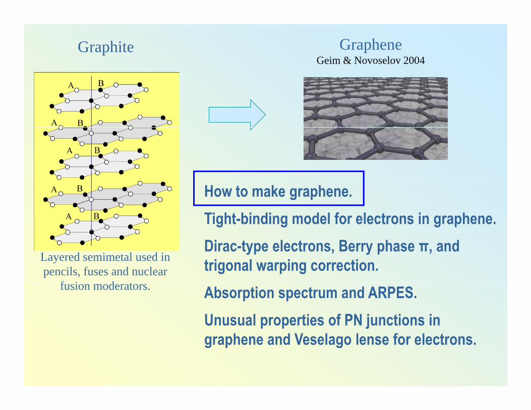
Graphite GrapheneGeim & Novoselov 2004
How to make graphene.Tight-binding model for electrons in graphene.
Layered semimetal used in pencils, fuses and nuclear
f i d t
Dirac-type electrons, Berry phase π, and trigonal warping correction.
fusion moderators. Absorption spectrum and ARPES.Unusual properties of PN junctions in
h d V l l f l tgraphene and Veselago lense for electrons.

‘Do It Yourself’graphene
Geim & Novoselov(Manchester) 2004
Mechanical exfoliation: the favourite method of
h i d iwww.grapheneindustries.comto make individual10-100 µm flakes.
Graphene from a ‘nanopensil’Kim (Columbia Univ) 2005 10 µm10 µm

High-tech graphene: grown epitaxially by solid state graphitization of Si-face of SiC (Si sublimation from the surface)
Lauffer, Emtsev, Graupner, au e , sev, G aup e ,Seyller (Erlangen), LeyPRB 77, 155426 (2008)
10 nm
5 mm
Tzalenchuk, Lara-Avila, Kalaboukhov, Paolillo, Syväjärvi,
kiYakimova (Linkoping),Kazakova, Janssen, VF, Kubatkin, arXiv:0909.1220 Nature Nanotechnology - in press
Gaskill et al, (HRL Malibu) ECS Trans. 19, 117 (2009) 10 µm

How to make graphene.
Tight-binding model for electrons in graphene.
Dirac-type electrons, Berry phase π, and trigonal warping correction.
Graphene optical absorption and ARPES.
Absence of back-scattering of electrons from electrostatic potentialfrom electrostatic potential.
Unusual properties of PN junctions in h d V l l f graphene and Veselago lense for
electrons.

hybridisation forms strong directed bonds2sp
4 electrons in the outer s-p shell of carbon
hybridisation forms strong directed bonds which determine a honeycomb lattice structure.p
C
- bonds
)(zp orbitals determine conduction properties of graphite
0)(p orbitals determine conduction properties of graphite
AB
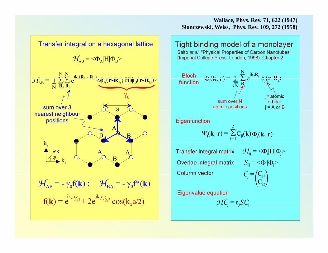
Wallace, Phys. Rev. 71, 622 (1947)Slonczewski, Weiss, Phys. Rev. 109, 272 (1958)

Wallace, Phys. Rev. 71, 622 (1947)Slonczewski, Weiss, Phys. Rev. 109, 272 (1958)

221121ananR nn
221121nn
A4.121 aaa
121 nnRGie
2G
GNGNG
Reciprocal latticea
221121GNGNG NN
aGaG 1111
2||;
G
unitcell
aGaG
S
2
111
2||;
||;
1G
unitcellSGaG 222 ||;

Reciprocal lattice
GNGNG
)()( kGk
Hexagonal
221121GNGNG NN )()(
21kGk NN
Hexagonal reciprocal lattice corresponding to
the hexagonalG the hexagonal
Bravais lattice2G
1st Brilloun zone
1G
1G

Fermi ‘point’in graphenein graphene
FEk )(
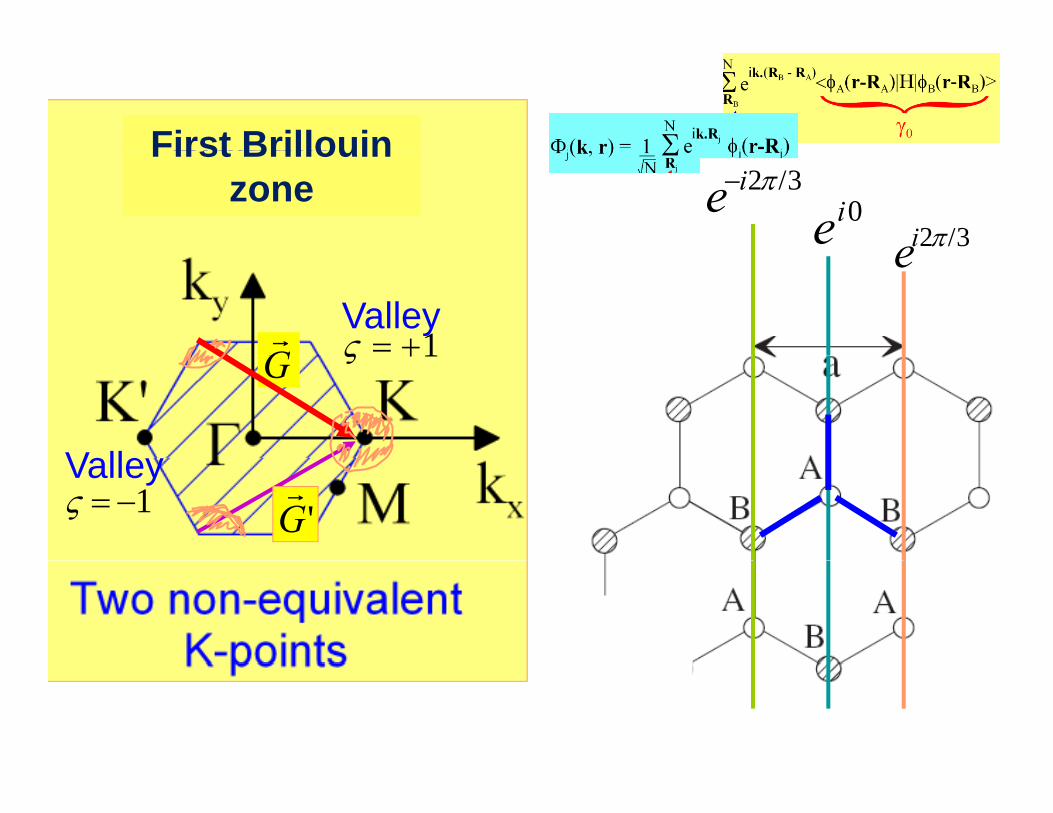
First BrillouinFirst Brillouinzone 0ie 3/2ie
3/2ie
G Valley
1
e
G
V ll
1
'G1
Valley

)()(0,
32232
332232 y
ax
ay
ay
ax
a ppiipippiiKAB eeeeeH
vippaH KBA )(023
)(023
yx ippa vippaH yxKBA )(02,
Bloch function amplitudes (e.g., in the valley K) on the AB sites (‘isospin’) mimic spinK) on the AB sites ( isospin ) mimic spin
components of a massless relativistic particle.
A
(valleys) 0
B
p
(valleys)
pvipp
ippvH
yx
yx
00ˆ
sec8
023 10~ cmav
pp yx McClure, PR 104, 666 (1956)

valley indexvalley index‘pseudospin’
1
B
A
vH
,
00
ˆ
A
B
vH
0
0pp
A
sublattice indexyx ipp ‘isospin’
yx ipp
Also, one may need to take into account an additional real spin degeneracy of all states

Bloch function amplitudes (e.g., in the valley K) on the AB sites (‘isospin’) mimic spin
ii
ppp )sin,cos(
components of a relativistic Dirac fermion.
A
i
yx
iyx
peipp
peipp
0
B
isospin direction is
nvppvvH
0
0 isospin direction is linked to the axis
determined by the electron momentum.for conduction band
electrons,pvp
1n
1
p
ip e1
21 xpyp
valence band (‘holes’)1np

F pvH
B
A
F
conduction band )sincos( ppp conduction band
1n p)sin,cos( ppp
sublattice ‘isospin’ is linked to the direction of the electron
1
1
valence band 1n p
of the electron momentum
ip e21
)( pn Berry phase
3
322 ii
ee d2
32 ee
dddi
0
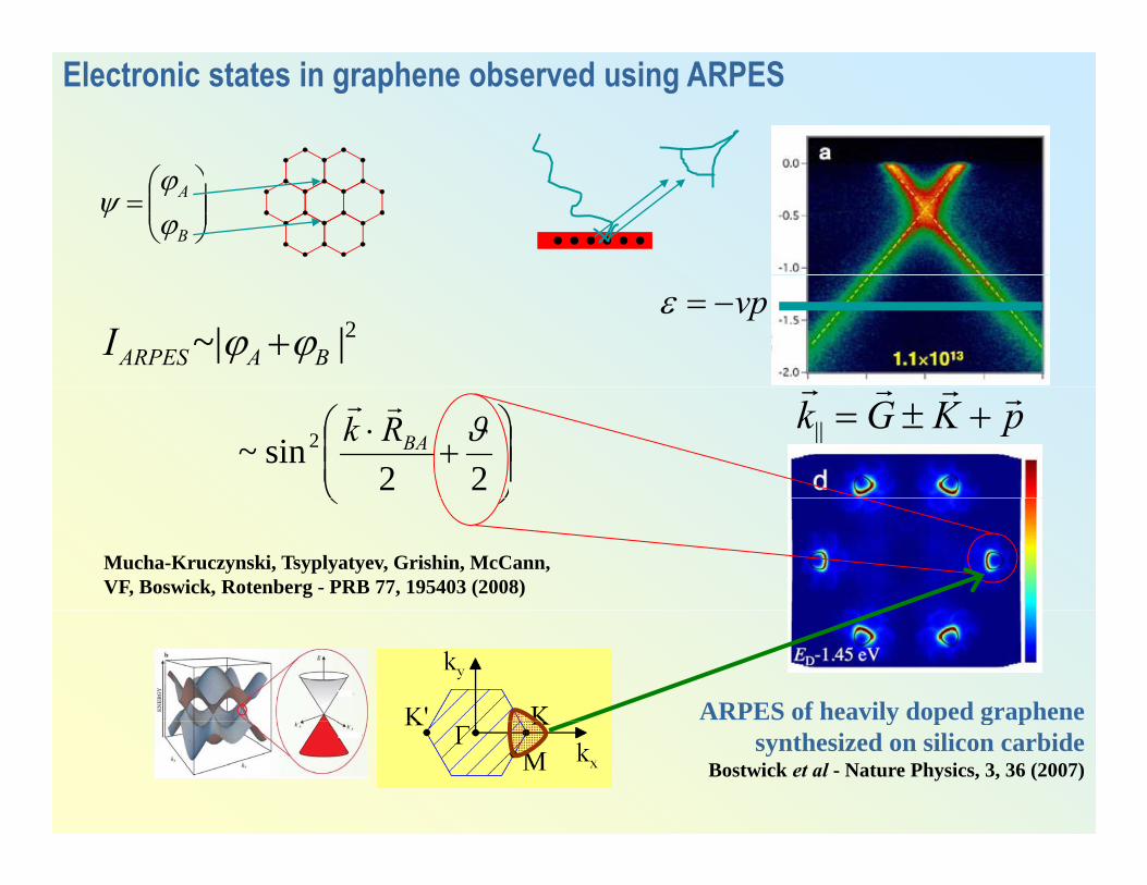
Electronic states in graphene observed using ARPES
B
A
vp2|~| BAARPESI
pKGk ||
22
sin~ 2 BARk
Mucha-Kruczynski, Tsyplyatyev, Grishin, McCann, VF, Boswick, Rotenberg - PRB 77, 195403 (2008)
ARPES of heavily doped grapheney p g psynthesized on silicon carbide
Bostwick et al - Nature Physics, 3, 36 (2007)

0)(0
00ˆ
2
2
vH
weak ‘trigonal warping
0)(0
)()(
32232
332232 y
ax
ay
ay
ax
a ppiipippiiH
valley 1
0,322333223 yyy
KAB eeeeeH 2
8023 )()(
20
yxa
yx ippippa
)(
i
iyx
peipp
peipp
Fp )( yx peipp
)sin,cos( ppp
KKpp
tt
;
time-inversionsymmetry
A. Bostwick et al – Nature Physics 3, 36 (2007)
pp ;

How to make graphene.
Tight-binding model for electrons in graphene.
Dirac-type electrons, Berry phase π, and trigonal warping correction.
Graphene optical absorption and ARPES.
Absence of back-scattering of electrons from electrostatic potentialfrom electrostatic potential.
Unusual properties of PN junctions in h d V l l f graphene and Veselago lense for
electrons.
Absorption of light by graphene membrane
pvH
H v
ce
pH
ce
e2ceg
/
1
1
%3.22
ce
Gusynin, Sharapov, Carbotte - PRL 96, 256802 (2006) Gusynin Sharapov - PRB B 73 245411 (2006)
Nair, Blake, Grigorenko, Novoselov, Booth, Stauber, Peres, Geim - Science (2008)
Gusynin, Sharapov - PRB B 73, 245411 (2006) Nilsson, Castro Neto, Guinea, Peres, - PRL 97, 266801 (2006)
Abergel, VF - PRB B 75, 155430 (2007)

Visibility of graphene flakes on SiO /Si substrateon SiO2/Si substrate
ssph2sin
s
N 212
o
nms10
300
o10
1o
ms10
1
Abergel, Russell, VF - Appl. Phys. Lett. 91, 063125 (2007) Blake, Hill, Castro Neto, Novoselov, Jiang, Yang, Booth, Geim - Appl. Phys. Lett. 91, 063124 (2007)

How to make graphene.
Tight-binding model for electrons in graphene.
Dirac-type electrons, Berry phase π, and trigonal warping correction.
Graphene optical absorption and ARPES.
Absence of back-scattering of electrons from electrostatic potentialfrom electrostatic potential.
Unusual properties of PN junctions in h d V l l f graphene and Veselago lense for
electrons.

Monolayer graphene: two-dimensional gapless semiconductor with the Dirac-type spectrum of electrons
DoS6
4K
140K
bandvalence
bandconduction
2
4
(k
)
280K
140K
gatecarriers Vn band band
04-4 0
n (1012 cm-2)
K. Novoselov et al., Science 306, 666 (2004)
vp
xpyp

nvppvvH
0
0
0
isospin direction is linked to the electron momentum.
ip e
12
1
vp for conduction band electrons
1n p
1
xpyp
1n
1n p Due to the isospin conservation, A-B symmetric
1n
valence band conservation, A B symmetric
potential cannot backward scatter chiral fermions,
Ando, Nakanishi, Saito J Ph S J 67 2857 (1998)
)(wJ. Phys. Soc. Jpn 67, 2857 (1998)
)(
|)'(|cos~)( 22 ppfw

PN junctions in the usual gap-full semiconductors are non-transparent for incident electrons therefore they are highly resistivetransparent for incident electrons, therefore, they are highly resistive.
PN junctions in in graphene are different.

Transmission of chiral electrons through the PN junction in graphene
vp vpc
Fp/
'2Fh
F
pN
vpeU
vpv Fp
/2Fe
F
pN
vpeU
conduction band electrons
1n p1nDue to the isospin conservation, A-B symmetric potential
cannot backward scatter chiral electrons cannot backward scatter chiral electrons
For graphene PN junctions: Cheianov, VF - PR B 74, 041403 (2006)pvH ˆ For graphene PN junctions: Cheianov, VF PR B 74, 041403 (2006)‘Klein paradox’: Katsnelson, Novoselov, Geim, Nature Physics 2, 620 (2006)pvH

Transmission of chiral electrons through the PN junction in graphene
0U
ip
12
1
)(sin 222 xUpp Fx
ip e2
d
Due to the ‘isospin’ conservation, 2sin cos)(
2dpFew 1p ,
electrostatic potential U(x) which smooth on atomic distances cannot scatter chiral fermions in the exactly
1
backward direction. dkF/1

Transmission of chiral electrons through the PN junction in graphene
L
d
dp
he
Lg Fnp
22
Due to transmission of electrons with a small incidence angle, θ<1/pFd , a PN junction in graphene should display a finite conductance (no pinch-off) dhL
eIII )1( 21
should display a finite conductance (no pinch off)
A characteristic Fano factor in the shot noise: )( 2
Cheianov, VF - PR B 74, 041403 (2006)

PN junctions should be taken into consideration in
t t i l d i two-terminal devices, since metallic contacts
dope graphene, due to the p g pwork function difference.
Heersche et al - Nature Physics (2007)
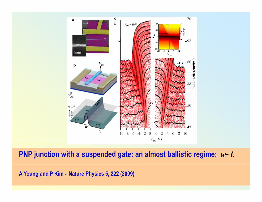
w
PNP junction with a suspended gate: an almost ballistic regime: w~l.
A Young and P Kim - Nature Physics 5, 222 (2009)

Wishful thinking about graphene microstructuresFocusing and Veselago lens for electrons in ballistic graphene
Cheianov, VF, Altshuler - Science 315, 1252 (2007)
pvppc
)( Fermi momentum
/
'2v
pN
vpeU
ppv
pv
vppv
)(
cp/vh pN
ppv
pv
vp
Fermi momentum/2
ce
c
pN
vpeU
vp
The effect we’ll discuss would be the strongest in sharp PN junction, ith d λwith d~λF .

vvccyy pppp sinsin' PN junction
cV
nppvc
sinsin
ppcvsin
Snell’s law with negative
cnegative
refraction index
v'p
pvVvp cc
;
n-type
''vpv
vVp-type
pVp cc ;
''ppvVv

vc pp vc pp

cv pp 8.0 cv pp

Veselago Lens for photonsg p
Veselago, Sov. Phys.-Usp., 10, 509 (1968) Pendry, Phys. Rev. Lett., 85, 3966 (2000)
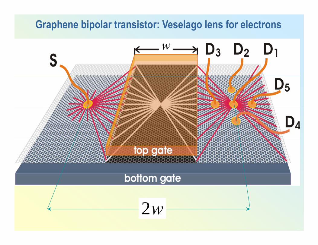
Graphene bipolar transistor: Veselago lens for electrons
ww
w2

How to make graphene.
Tight-binding model for electrons in graphene, Dirac-type electrons, Berry phase π, and trigonal warping correction, graphene optics and ARPES.
Absence of back-scattering of electrons from Absence of back scattering of electrons from electrostatic potential and unusual properties of PN junctions in graphene and Veselago lense for electronselectrons.
Lecture III:Electronic properties of bilayer graphene, Landau levels in monolayers and bilayers, and the Quantum Hall effect.and the Quantum Hall effect.