electronics i – amplifiers, noise, and signal processing
TRANSCRIPT
Solid State Detectors and Electronics – Electronics I Helmuth SpielerTRIUMF Summer Institute 2007 LBNL
1
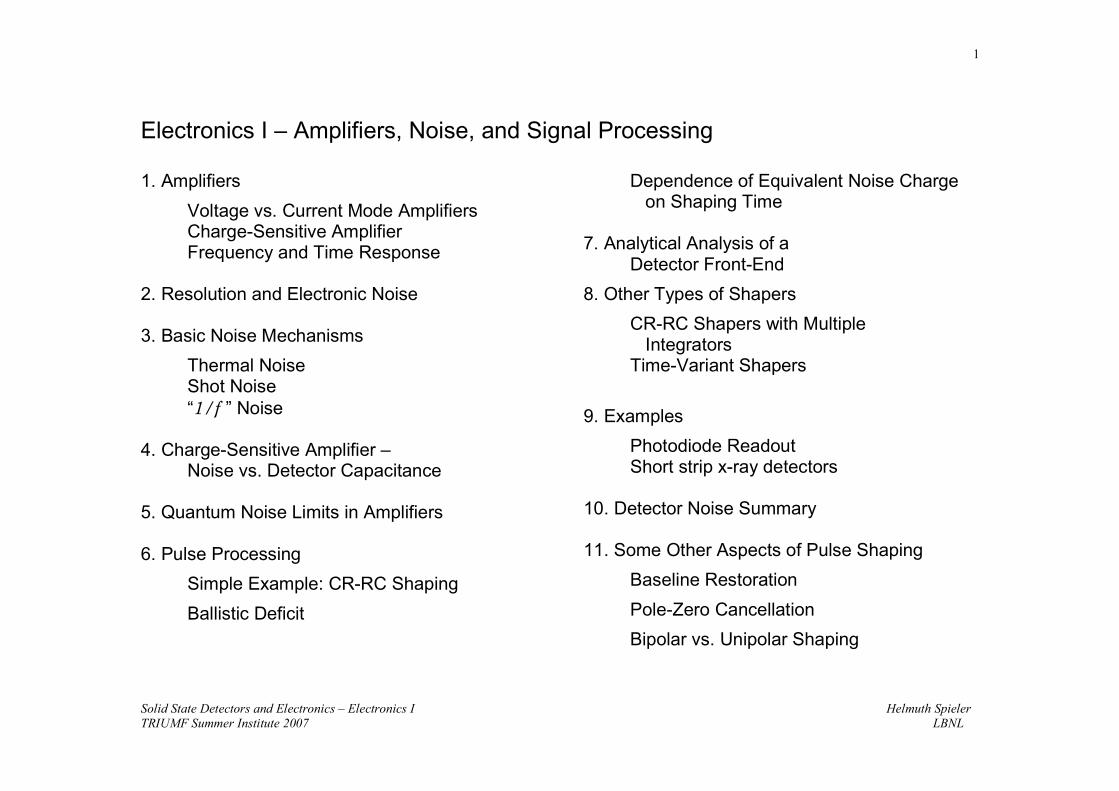
Electronics I – Amplifiers, Noise, and Signal Processing
1. AmplifiersVoltage vs. Current Mode AmplifiersCharge-Sensitive AmplifierFrequency and Time Response
2. Resolution and Electronic Noise
3. Basic Noise MechanismsThermal NoiseShot Noise“1/f ” Noise
4. Charge-Sensitive Amplifier –Noise vs. Detector Capacitance
5. Quantum Noise Limits in Amplifiers
6. Pulse ProcessingSimple Example: CR-RC ShapingBallistic Deficit
Dependence of Equivalent Noise Chargeon Shaping Time
7. Analytical Analysis of aDetector Front-End
8. Other Types of ShapersCR-RC Shapers with Multiple
IntegratorsTime-Variant Shapers
9. ExamplesPhotodiode ReadoutShort strip x-ray detectors
10. Detector Noise Summary
11. Some Other Aspects of Pulse ShapingBaseline RestorationPole-Zero CancellationBipolar vs. Unipolar Shaping
Solid State Detectors and Electronics – Electronics I Helmuth SpielerTRIUMF Summer Institute 2007 LBNL
2
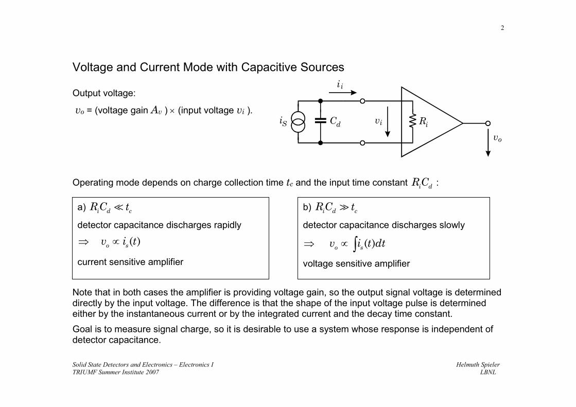
Voltage and Current Mode with Capacitive Sources
Output voltage:
vo = (voltage gain Av ) × (input voltage vi ).
Operating mode depends on charge collection time tc and the input time constant i dR C :
Note that in both cases the amplifier is providing voltage gain, so the output signal voltage is determineddirectly by the input voltage. The difference is that the shape of the input voltage pulse is determinedeither by the instantaneous current or by the integrated current and the decay time constant.Goal is to measure signal charge, so it is desirable to use a system whose response is independent ofdetector capacitance.
C Ri v
v
i
d iS i
o
i
a) i d cR C t
detector capacitance discharges rapidly
( )o sv i t⇒ ∝
current sensitive amplifier
b) i d cR C t
detector capacitance discharges slowly
( )o sv i t dt⇒ ∝ ∫voltage sensitive amplifier
Solid State Detectors and Electronics – Electronics I Helmuth SpielerTRIUMF Summer Institute 2007 LBNL
3
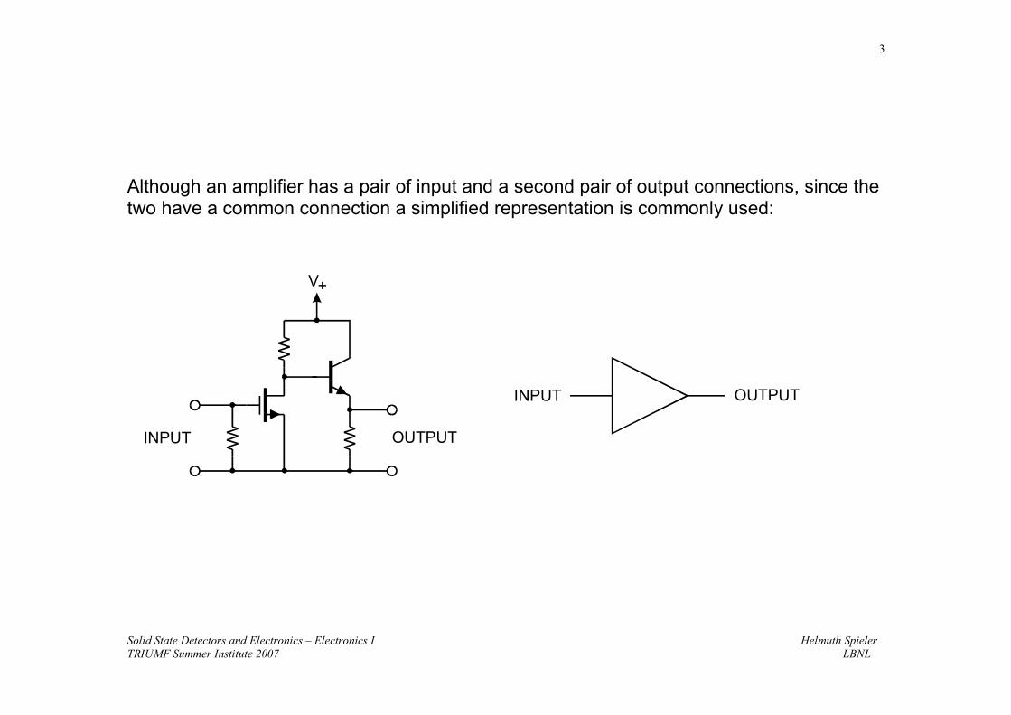
Although an amplifier has a pair of input and a second pair of output connections, since thetwo have a common connection a simplified representation is commonly used:
V+
INPUT
INPUT
OUTPUT
OUTPUT
Solid State Detectors and Electronics – Electronics I Helmuth SpielerTRIUMF Summer Institute 2007 LBNL
4
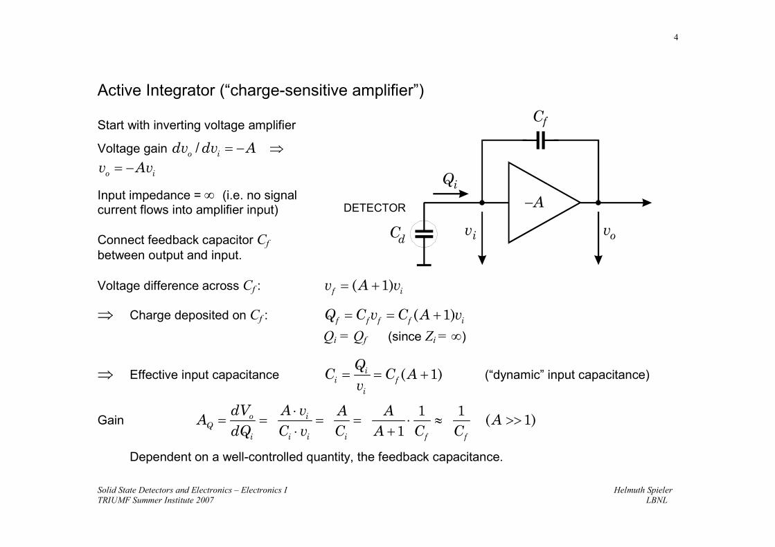
Active Integrator (“charge-sensitive amplifier”)
Start with inverting voltage amplifier
Voltage gain /o idv dv A= − ⇒
o iv Av= −
Input impedance = ∞ (i.e. no signalcurrent flows into amplifier input)
Connect feedback capacitor Cfbetween output and input.
Voltage difference across Cf : ( 1)f iv A v= +
⇒ Charge deposited on Cf : ( 1)f f f f iQ C v C A v= = +Qi = Qf (since Zi = ∞)
⇒ Effective input capacitance ( 1)ii f
i
QC C A
v= = + (“dynamic” input capacitance)
Gain1 1
( 1)1
o iQ
i i i i f f
dV A v A AA A
dQ C v C A C C⋅
= = = = ⋅ ≈ >>⋅ +
Dependent on a well-controlled quantity, the feedback capacitance.
v
Q
C
C vi
i
f
d o
−ADETECTOR
Solid State Detectors and Electronics – Electronics I Helmuth SpielerTRIUMF Summer Institute 2007 LBNL
5
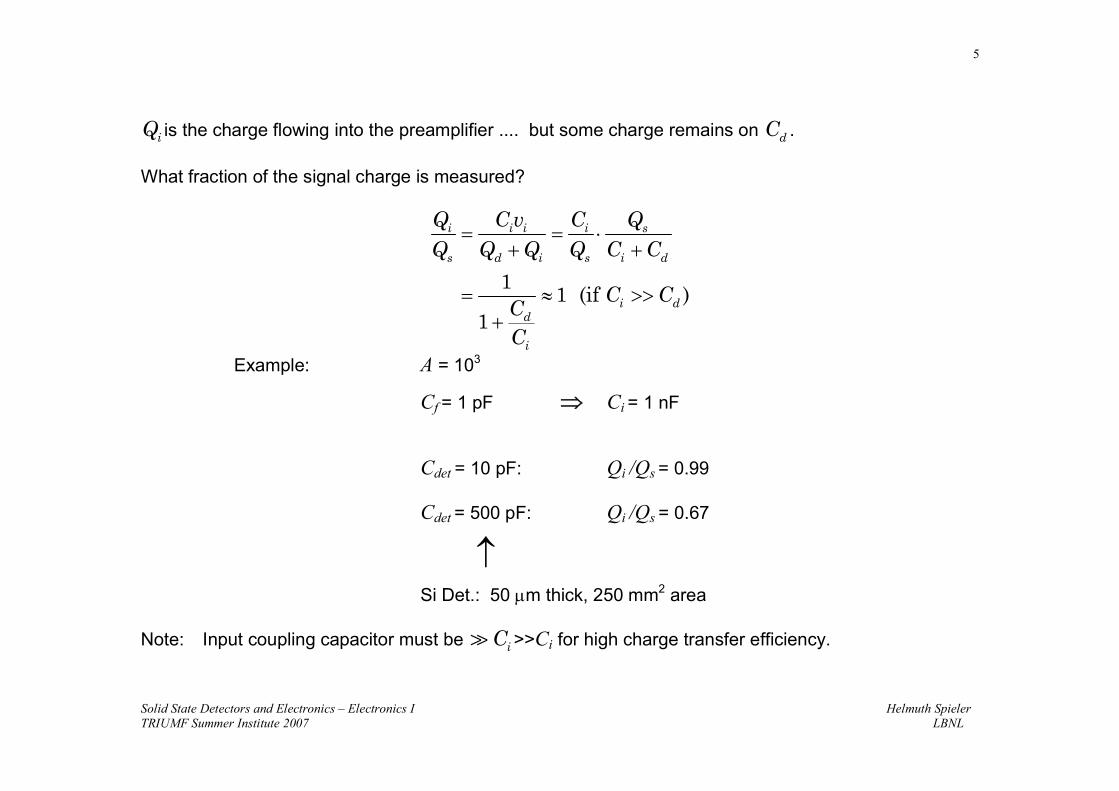
iQ is the charge flowing into the preamplifier .... but some charge remains on dC .
What fraction of the signal charge is measured?
11 (if )
1
i i i i s
s d i s i d
i dd
i
Q C v C QQ Q Q Q C C
C CCC
= = ⋅+ +
= ≈ >>+
Example: A = 103
Cf = 1 pF ⇒ Ci = 1 nF
Cdet = 10 pF: Qi /Qs = 0.99
Cdet = 500 pF: Qi /Qs = 0.67
↑Si Det.: 50 µm thick, 250 mm2 area
Note: Input coupling capacitor must be iC >>Ci for high charge transfer efficiency.
Solid State Detectors and Electronics – Electronics I Helmuth SpielerTRIUMF Summer Institute 2007 LBNL
6
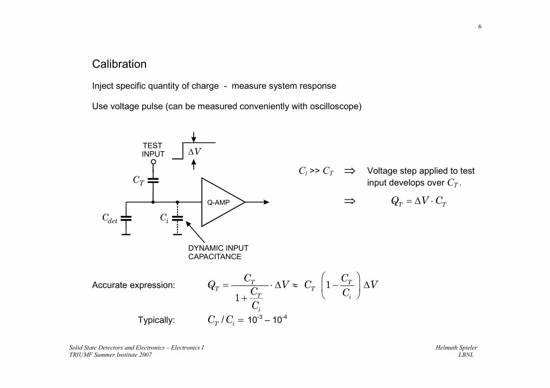
Calibration
Inject specific quantity of charge - measure system response
Use voltage pulse (can be measured conveniently with oscilloscope)
Ci >> CT ⇒ Voltage step applied to testinput develops over CT .
⇒ T TQ V C= ∆ ⋅
Accurate expression: 11
T TT T
T i
i
C CQ V C V
C CC
= ⋅ ∆ ≈ − ∆
+
Typically: /T iC C = 10-3 – 10-4
C
C
C i
T
det
Q-AMP
∆VTESTINPUT
DYNAMIC INPUTCAPACITANCE
Solid State Detectors and Electronics – Electronics I Helmuth SpielerTRIUMF Summer Institute 2007 LBNL
7
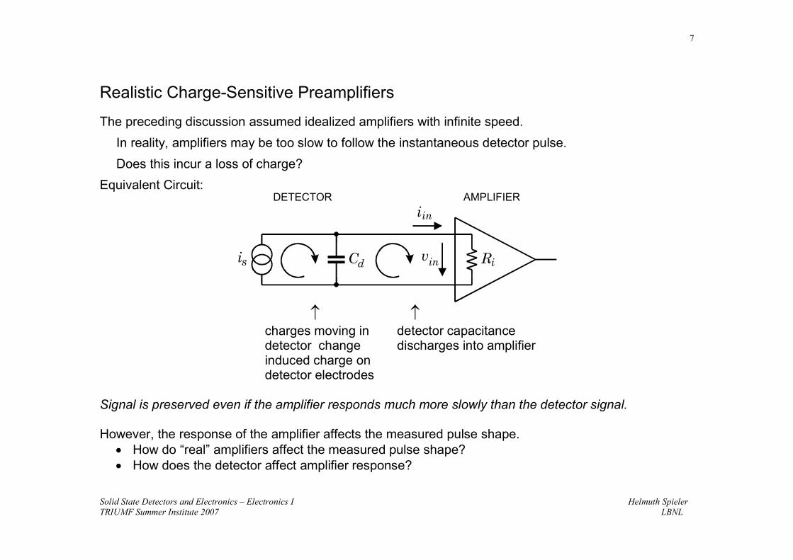
Realistic Charge-Sensitive Preamplifiers
The preceding discussion assumed idealized amplifiers with infinite speed.In reality, amplifiers may be too slow to follow the instantaneous detector pulse.Does this incur a loss of charge?
Equivalent Circuit:DETECTOR
C R
AMPLIFIER
i v
i
s ind
in
i
↑ ↑charges moving in detector capacitancedetector change discharges into amplifierinduced charge ondetector electrodes
Signal is preserved even if the amplifier responds much more slowly than the detector signal.
However, the response of the amplifier affects the measured pulse shape.• How do “real” amplifiers affect the measured pulse shape?• How does the detector affect amplifier response?

Solid State Detectors and Electronics – Electronics I Helmuth SpielerTRIUMF Summer Institute 2007 LBNL
8
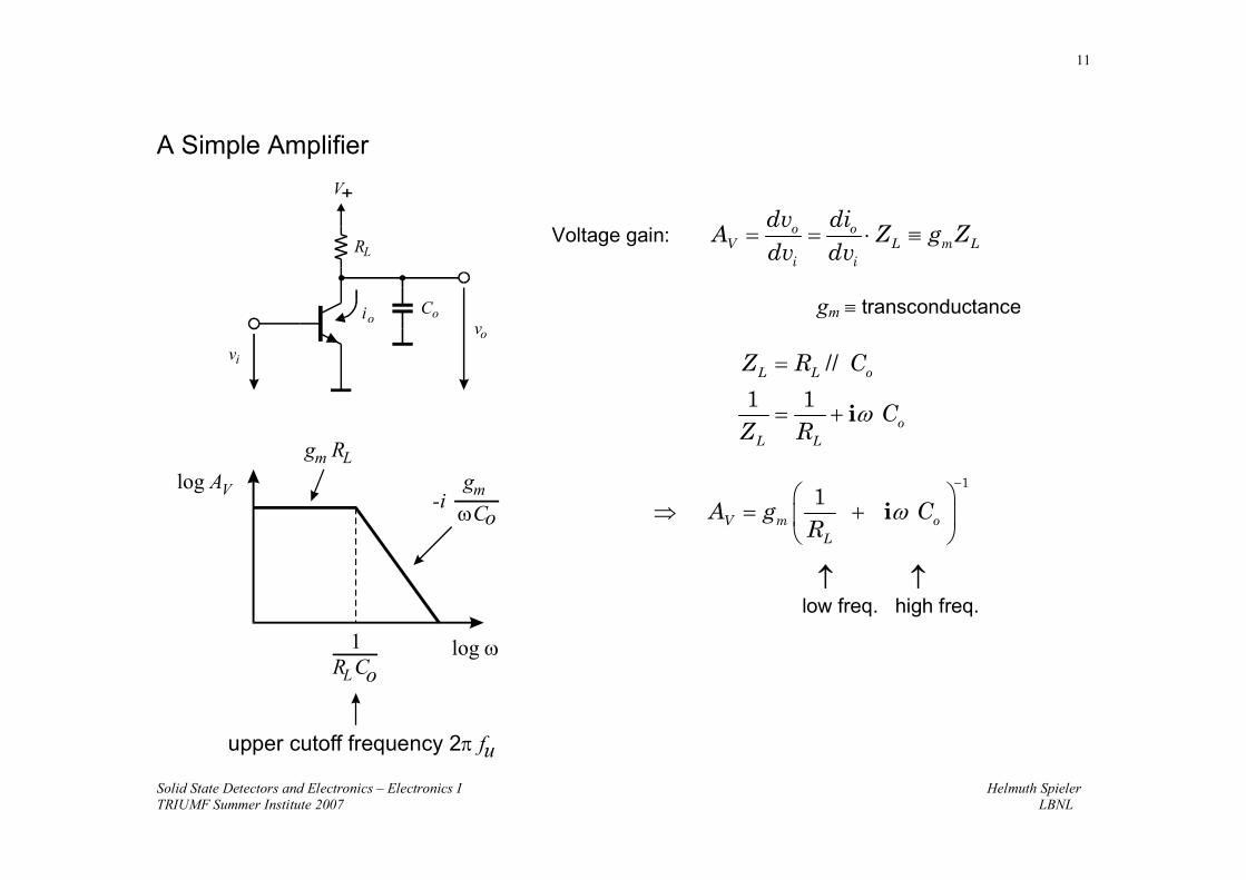
A Simple Amplifier
Voltage gain: o oV L m L
i i
dv diA Z g Z
dv dv= = ⋅ ≡
gm ≡ transconductance
//
1 1L L o
oL L
Z R C
CZ R
ω
=
= + i
11
V m oL
A g CR
ω−
⇒ = +
i
↑ ↑low freq. high freq.
V+
v
i C
R
v
i
o o
L
o
log A
log ω
V
g R
R
g
1
m L
L
m-i ωC
C
o
o
upper cutoff frequency 2π fu
Solid State Detectors and Electronics – Electronics I Helmuth SpielerTRIUMF Summer Institute 2007 LBNL
9
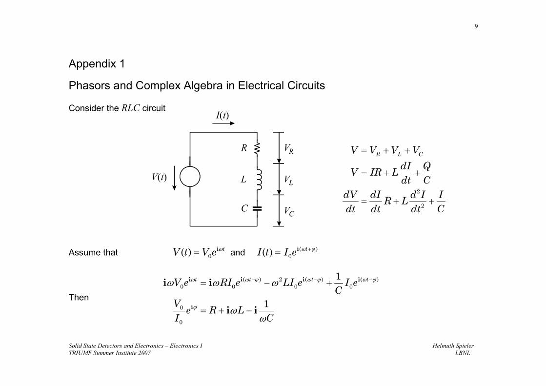
Appendix 1
Phasors and Complex Algebra in Electrical Circuits
Consider the RLC circuit
2
2
R L CV V V V
dI QV IR L
dt CdV dI d I I
R Ldt dt dt C
= + +
= + +
= + +
Assume that 0( ) tV t V e ω= i and ( )0( ) tI t I e ω ϕ+= i
Then
( ) 2 ( ) ( )0 0 0 0
0
0
1
1
t t t tV e RI e LI e I eC
Ve R L
I C
ω ω ϕ ω ϕ ω ϕ
ϕ
ω ω ω
ωω
− − −= − +
= + −
i i i i
i
i i
i i
I t( )
V t( )
C
L
R V
V
V
R
L
C

Solid State Detectors and Electronics – Electronics I Helmuth SpielerTRIUMF Summer Institute 2007 LBNL
10
Thus, we can express the total impedance 0 0( / )Z V I e ϕ≡ i of the circuit as a complexnumber with the magnitude 0 0/Z V I= and phase ϕ.
In this representation the equivalent resistances (reactances) of L and C are imaginarynumbers
ω=LX Li andω
= −CXCi .
Plotted in the complex plane:
Relative to VR, the voltageacross the inductor VL isshifted in phase by +90°.
The voltage across thecapacitor VC is shifted inphase by -90°.
Use to represent any element that introduces a phase shift, e.g. an amplifier. A phase shiftof +90° appears as +i , -90° as −i .
Re
Im
R
Z
i iω ωL C- /
iωL
- /i ωC
Solid State Detectors and Electronics – Electronics I Helmuth SpielerTRIUMF Summer Institute 2007 LBNL
11
A Simple Amplifier
Voltage gain: o oV L m L
i i
dv diA Z g Z
dv dv= = ⋅ ≡
gm ≡ transconductance
//
1 1L L o
oL L
Z R C
CZ R
ω
=
= + i
11
V m oL
A g CR
ω−
⇒ = +
i
↑ ↑low freq. high freq.
V+
v
i C
R
v
i
o o
L
o
log A
log ω
V
g R
R
g
1
m L
L
m-i ωC
C
o
o
upper cutoff frequency 2π fu
Solid State Detectors and Electronics – Electronics I Helmuth SpielerTRIUMF Summer Institute 2007 LBNL
12
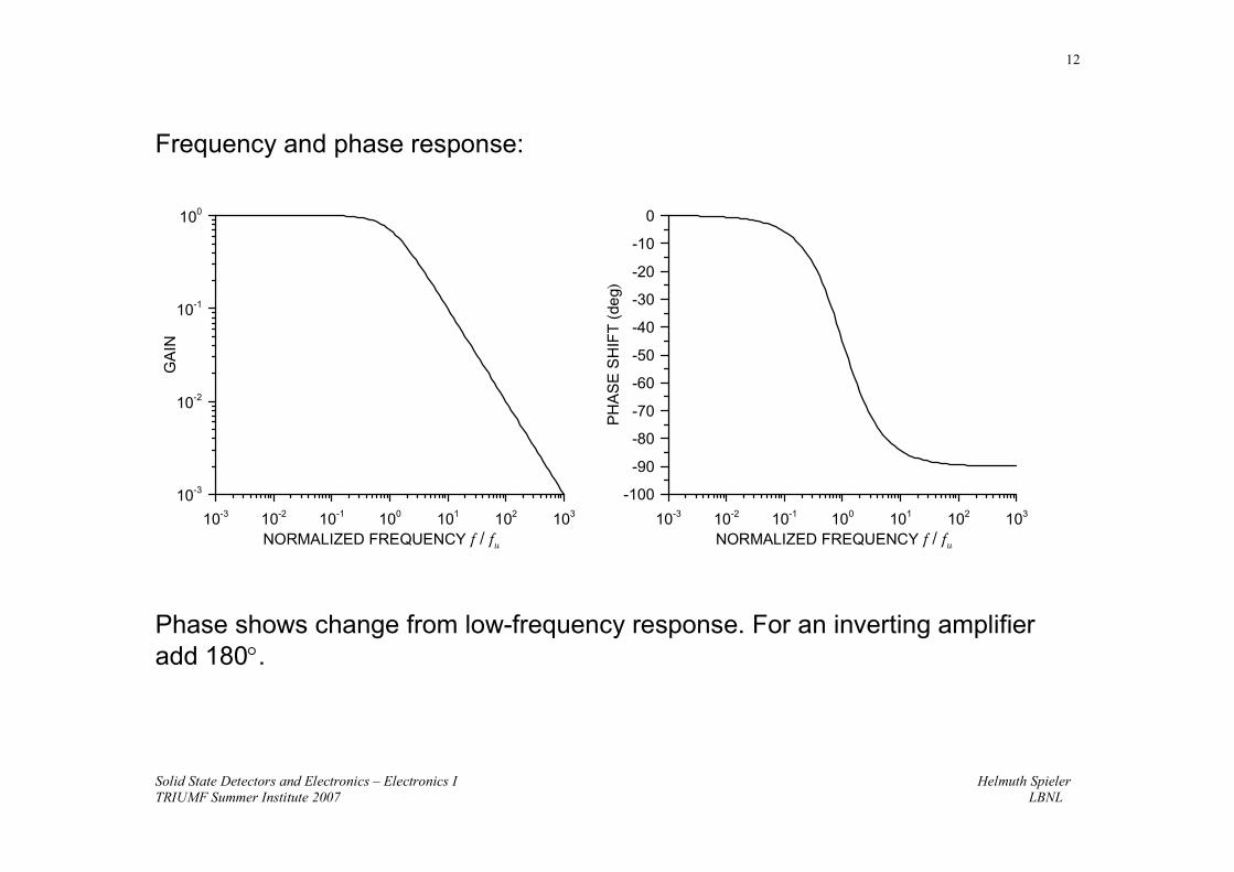
Frequency and phase response:
Phase shows change from low-frequency response. For an inverting amplifieradd 180°.
10-3 10-2 10-1 100 101 102 103
NORMALIZED FREQUENCY f / fu
10-3
10-2
10-1
100
GA
IN
10-3 10-2 10-1 100 101 102 103
NORMALIZED FREQUENCY f / fu
-100
-90
-80
-70
-60
-50
-40
-30
-20
-10
0
PHA
SE S
HIF
T (d
eg)

Solid State Detectors and Electronics – Electronics I Helmuth SpielerTRIUMF Summer Institute 2007 LBNL
13
Pulse Response of the Simple Amplifier
A voltage step vi (t) at the input causes a current step io (t) at the output of the transistor.
For the output voltage to change, the output capacitance Co must first charge up.
⇒ The output voltage changes with a time constant τ = RLCo
The time constant τ corresponds to the upper cutoff frequency :1
2 ufτ
π=
log A
log ω
v
v0
v
UPPER CUTOFF FREQUENCY 2π fu
V0
FREQUENCY DOMAIN TIME DOMAIN
INPUT OUTPUT
A
A = 1ω0 V = V t
0( )1 exp( / )− − τ
RR
1L
L
CCo
o
g Rm Lgm−i ωCo
τ =

Solid State Detectors and Electronics – Electronics I Helmuth SpielerTRIUMF Summer Institute 2007 LBNL
14
Input Impedance of a Charge-Sensitive Amplifier
Input impedance ( 1)1
f fi
Z ZZ A
A A= ≈ >>
+
Amplifier gain vs. frequency beyond the upper cutoff frequency
0Aωω
= −i
Feedback impedance1
ff
ZCω
= −i
⇒ Input Impedance0
1i
f
ZC ωω
ω
= − ⋅−
i
i
0
1i
f
ZCω
=
Imaginary component vanishes ⇒ Resistance: Zi → Ri
⇒ low frequencies ( f < fu): capacitive inputhigh frequencies ( f > fu): resistive input
Gain-Bandwidth Product
Solid State Detectors and Electronics – Electronics I Helmuth SpielerTRIUMF Summer Institute 2007 LBNL
15
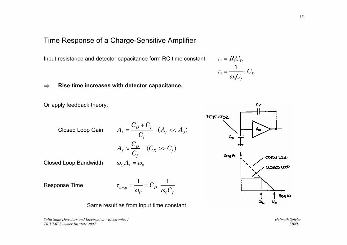
Time Response of a Charge-Sensitive Amplifier
Input resistance and detector capacitance form RC time constant i i DR Cτ =
0
1i D
f
CC
τω
= ⋅
⇒ Rise time increases with detector capacitance.
Or apply feedback theory:
Closed Loop Gain 0( )D ff f
f
C CA A A
C
+= <<
( )Df D f
f
CA C C
C≈ >>
Closed Loop Bandwidth 0C fAω ω=
Response Time0
1 1amp D
C f
CC
τω ω
= =
Same result as from input time constant.
Solid State Detectors and Electronics – Electronics I Helmuth SpielerTRIUMF Summer Institute 2007 LBNL
16
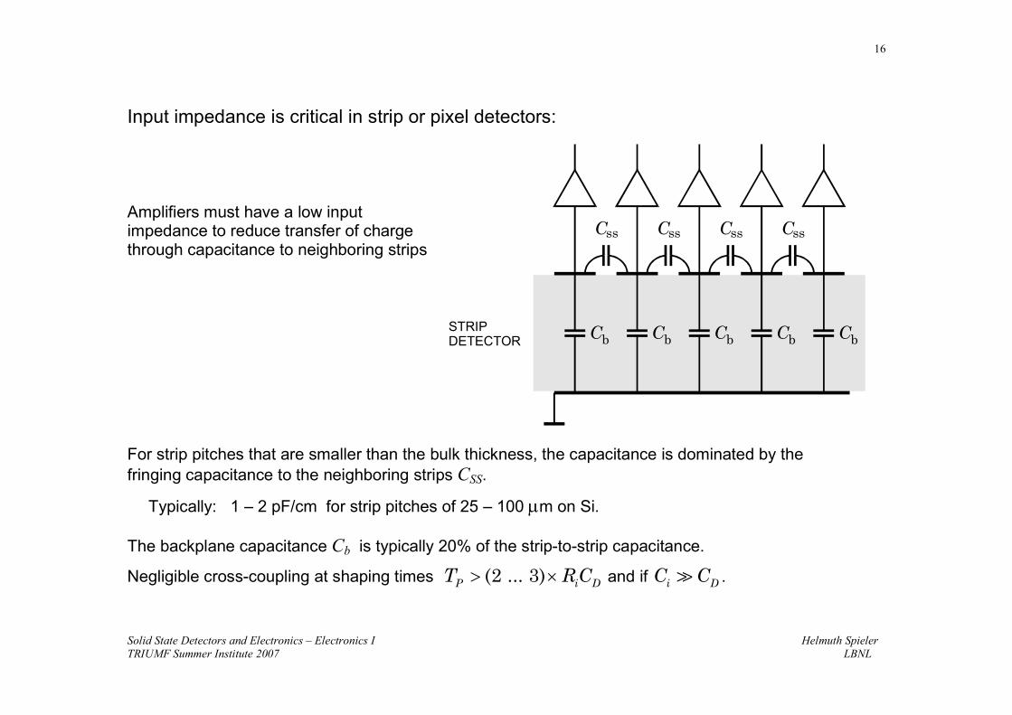
Input impedance is critical in strip or pixel detectors:
Amplifiers must have a low inputimpedance to reduce transfer of chargethrough capacitance to neighboring strips
For strip pitches that are smaller than the bulk thickness, the capacitance is dominated by thefringing capacitance to the neighboring strips CSS.
Typically: 1 – 2 pF/cm for strip pitches of 25 – 100 µm on Si.
The backplane capacitance Cb is typically 20% of the strip-to-strip capacitance.
Negligible cross-coupling at shaping times (2 ... 3)P i DT R C> × and if i DC C .
C C C C
C C C C C
ss ss ss ss
b b b b bSTRIPDETECTOR
Solid State Detectors and Electronics – Electronics I Helmuth SpielerTRIUMF Summer Institute 2007 LBNL
17
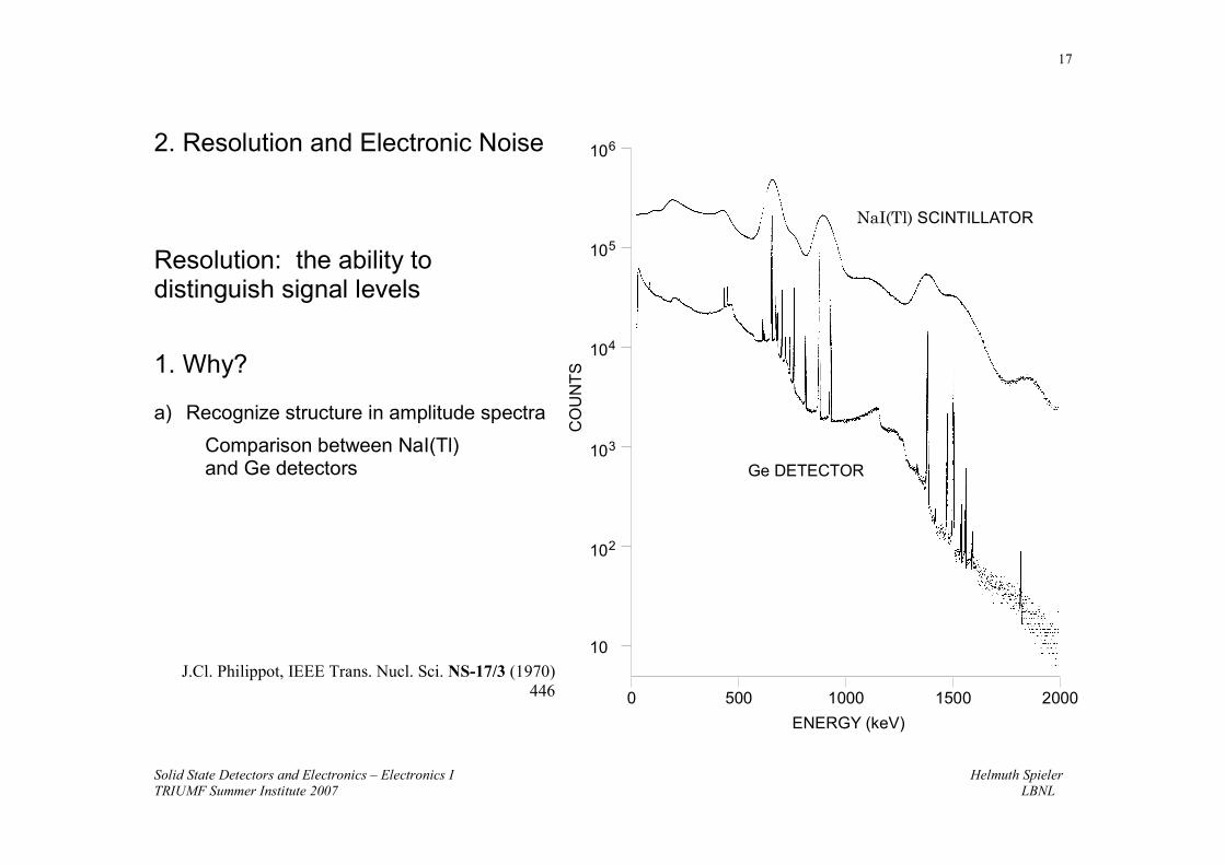
2. Resolution and Electronic Noise
Resolution: the ability todistinguish signal levels
1. Why?
a) Recognize structure in amplitude spectraComparison between NaI(Tl)and Ge detectors
J.Cl. Philippot, IEEE Trans. Nucl. Sci. NS-17/3 (1970)446 0 500 1000 1500 2000
ENERGY (keV)
10
10
10
10
10
10
6
5
4
3
2
CO
UN
TS
NaI(Tl) SCINTILLATOR
Ge DETECTOR
Solid State Detectors and Electronics – Electronics I Helmuth SpielerTRIUMF Summer Institute 2007 LBNL
18
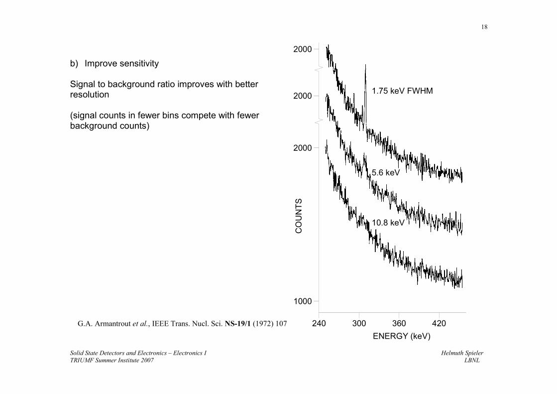
b) Improve sensitivity
Signal to background ratio improves with betterresolution
(signal counts in fewer bins compete with fewerbackground counts)
G.A. Armantrout et al., IEEE Trans. Nucl. Sci. NS-19/1 (1972) 107 240 300 360 420ENERGY (keV)
2000
2000
2000
1000
1.75 keV FWHM
5.6 keV
10.8 keV
CO
UN
TS

Solid State Detectors and Electronics – Electronics I Helmuth SpielerTRIUMF Summer Institute 2007 LBNL
19
What determines Resolution?
1. Signal Variance >> Baseline Variance
⇒ Electronic (baseline) noise not important
Examples: • High-gain proportional chambers
• Scintillation Counters with High-Gain PMTs
e.g. 1 MeV γ-rays absorbed by NaI(Tl) crystal
Number of photoelectrons: Npe ≈ 8.104 [MeV-1] × Eγ × QE ≈ 2.4.104
Variance typically: σpe = Npe1/2 ≈ 160 and σpe / Npe ≈ 5 - 8%
Signal at PMT anode (assume Gain= 104): Qsig= GPMT Npe ≈ 2.4.108 el andσsig= GPMT σpe ≈ 1.2.107 el
whereas electronic noise easily < 104 el
BASELINE BASELINE BASELINE
SIGNAL BASELINE NOISE SIGNAL + NOISE∗
Solid State Detectors and Electronics – Electronics I Helmuth SpielerTRIUMF Summer Institute 2007 LBNL
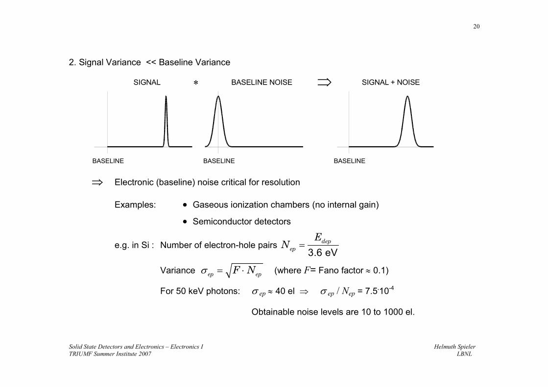
20
2. Signal Variance << Baseline Variance
⇒ Electronic (baseline) noise critical for resolution
Examples: • Gaseous ionization chambers (no internal gain)
• Semiconductor detectors
e.g. in Si : Number of electron-hole pairs3.6 eV
depep
EN =
Variance ep epF Nσ = ⋅ (where F= Fano factor ≈ 0.1)
For 50 keV photons: σ ep ≈ 40 el ⇒ σ ep / Nep = 7.5.10-4
Obtainable noise levels are 10 to 1000 el.
BASELINE BASELINE BASELINE
SIGNAL BASELINE NOISE SIGNAL + NOISE∗
Solid State Detectors and Electronics – Electronics I Helmuth SpielerTRIUMF Summer Institute 2007 LBNL
21
Baseline fluctuations can have many origins ...
pickup of external interference
artifacts due to imperfect electronics
… etc.,
but the (practical) fundamental limit is electronic noise.
Solid State Detectors and Electronics – Electronics I Helmuth SpielerTRIUMF Summer Institute 2007 LBNL
22
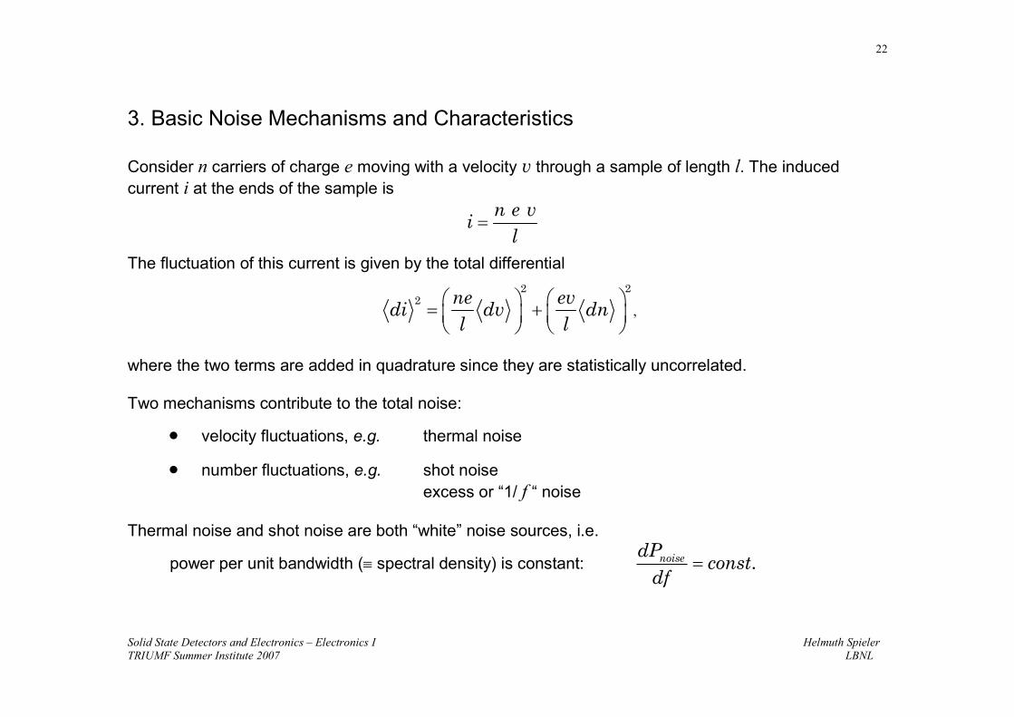
3. Basic Noise Mechanisms and Characteristics
Consider n carriers of charge e moving with a velocity v through a sample of length l. The inducedcurrent i at the ends of the sample is
n e vi
l=
The fluctuation of this current is given by the total differential2 2
2 ne evdi dv dn
l l = +
,
where the two terms are added in quadrature since they are statistically uncorrelated.
Two mechanisms contribute to the total noise:
• velocity fluctuations, e.g. thermal noise
• number fluctuations, e.g. shot noiseexcess or “1/ f “ noise
Thermal noise and shot noise are both “white” noise sources, i.e.
power per unit bandwidth (≡ spectral density) is constant: .noisedPconst
df=
Solid State Detectors and Electronics – Electronics I Helmuth SpielerTRIUMF Summer Institute 2007 LBNL
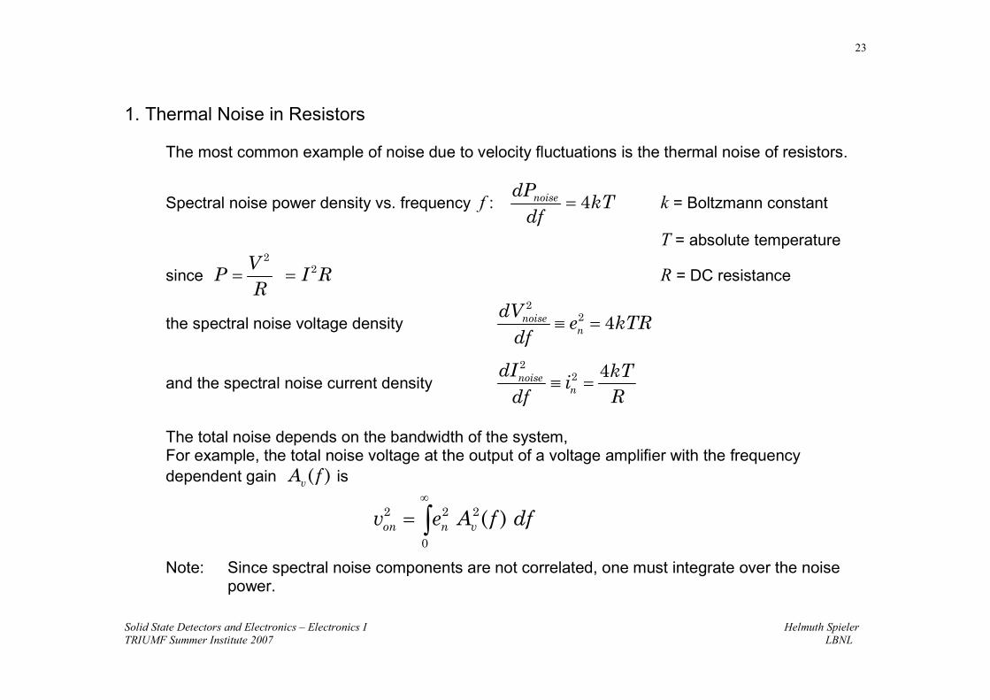
23
1. Thermal Noise in Resistors
The most common example of noise due to velocity fluctuations is the thermal noise of resistors.
Spectral noise power density vs. frequency f : 4noisedPkT
df= k = Boltzmann constant
T = absolute temperature
since2
2VP I R
R= = R = DC resistance
the spectral noise voltage density2
2 4noisen
dVe kTR
df≡ =
and the spectral noise current density2
2 4noisen
dI kTi
df R≡ =
The total noise depends on the bandwidth of the system,For example, the total noise voltage at the output of a voltage amplifier with the frequencydependent gain ( )vA f is
2 2 2
0
( )on n vv e A f df∞
= ∫Note: Since spectral noise components are not correlated, one must integrate over the noise
power.
Solid State Detectors and Electronics – Electronics I Helmuth SpielerTRIUMF Summer Institute 2007 LBNL
24
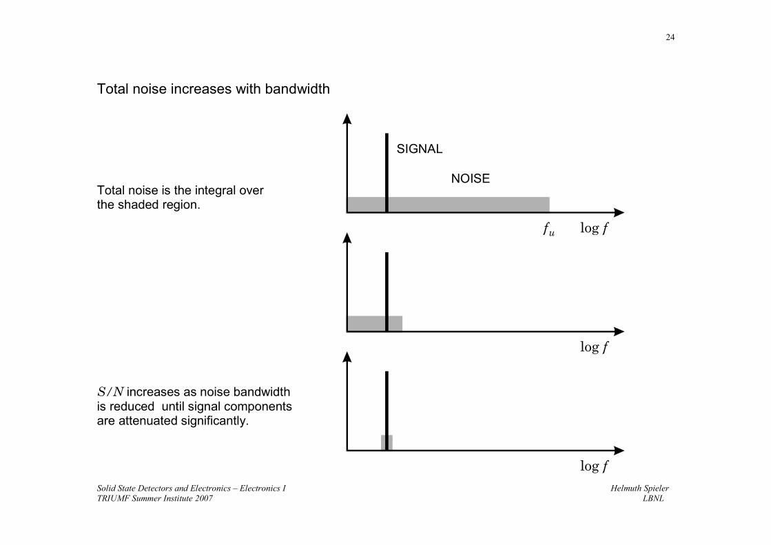
Total noise increases with bandwidth
Total noise is the integral overthe shaded region.
S/N increases as noise bandwidthis reduced until signal componentsare attenuated significantly.
log ff
log f
log f
SIGNAL
NOISE
u
Solid State Detectors and Electronics – Electronics I Helmuth SpielerTRIUMF Summer Institute 2007 LBNL
25
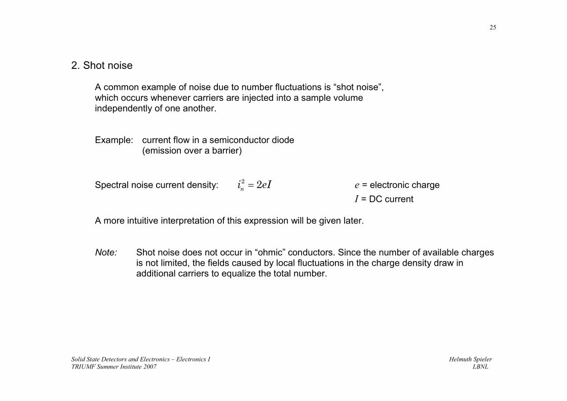
2. Shot noise
A common example of noise due to number fluctuations is “shot noise”,which occurs whenever carriers are injected into a sample volumeindependently of one another.
Example: current flow in a semiconductor diode(emission over a barrier)
Spectral noise current density: 2 2ni eI= e = electronic chargeI = DC current
A more intuitive interpretation of this expression will be given later.
Note: Shot noise does not occur in “ohmic” conductors. Since the number of available chargesis not limited, the fields caused by local fluctuations in the charge density draw inadditional carriers to equalize the total number.
Solid State Detectors and Electronics – Electronics I Helmuth SpielerTRIUMF Summer Institute 2007 LBNL
26
Noise Spectral Densities
Spectral Density of Thermal Noise (Johnson Noise)
Two approaches can be used to derive the spectral distribution of thermal noise.
1. The thermal velocity distribution of the charge carriers is used to calculate the time dependence of theinduced current, which is then transformed into the frequency domain.
2. Application of Planck’s theory of black body radiation.
The first approach clearly shows the underlying physics, whereas the second “hides” the physics byapplying a general result of statistical mechnics. However, the first requires some advanced conceptsthat go well beyond the standard curriculum, so the “black body” approach will be used.
In Planck’s theory of black body radiation the energy per mode
/ 1h kT
hE
e ν
ν=
−and the spectral density of the radiated power
/ 1h kT
dP hd e ν
νν
=−
i.e. this is the power that can be extracted in equilibrium.
Solid State Detectors and Electronics – Electronics I Helmuth SpielerTRIUMF Summer Institute 2007 LBNL
27
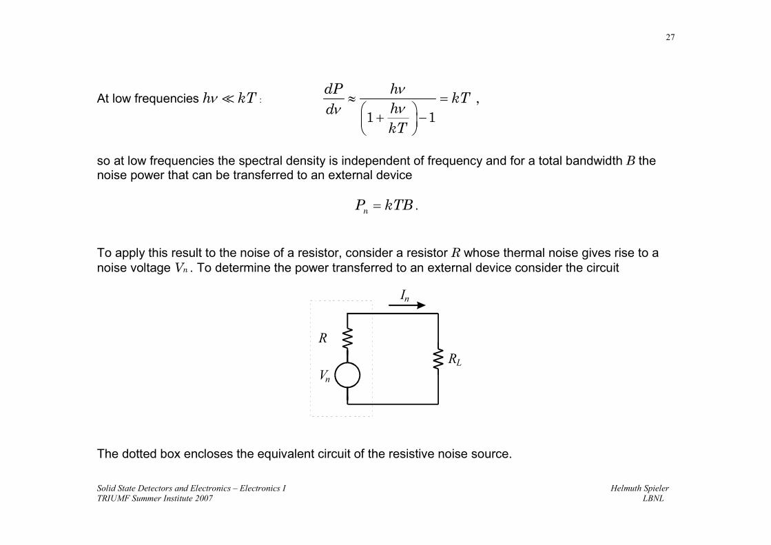
At low frequencies h kTν : ,1 1
dP hkT
hdkT
ννν
≈ = + −
so at low frequencies the spectral density is independent of frequency and for a total bandwidth B thenoise power that can be transferred to an external device
nP kTB= .
To apply this result to the noise of a resistor, consider a resistor R whose thermal noise gives rise to anoise voltage Vn . To determine the power transferred to an external device consider the circuit
The dotted box encloses the equivalent circuit of the resistive noise source.
RR
V
I
L
n
n
Solid State Detectors and Electronics – Electronics I Helmuth SpielerTRIUMF Summer Institute 2007 LBNL
28
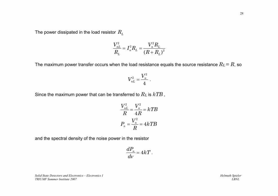
The power dissipated in the load resistor LR
2 22
2( )nL n L
n LL L
V V RI R
R R R= =
+
The maximum power transfer occurs when the load resistance equals the source resistance RL = R, so
22
4n
nL
VV = .
Since the maximum power that can be transferred to RL is kTB ,
2 2
2
4
4
nL n
nn
V VkTB
R RV
P kTBR
= =
= =
and the spectral density of the noise power in the resistor
4ndPkT
dν= .
Solid State Detectors and Electronics – Electronics I Helmuth SpielerTRIUMF Summer Institute 2007 LBNL
29
Spectral Density of Shot Noise
If an excess electron is injected into a device, it forms a current pulse of duration τ. In a thermionic diodeτ is the transit time from cathode to anode, for example. In a semiconductor diode τ is the recombinationtime. If these times are short with respect to the periods of interest 1/ fτ , the current pulse can berepresented by a δ pulse. The Fourier transform of a delta pulse yields a “white” spectrum, i.e. theamplitude distribution in frequency is uniform
, 2n pke
dIq
df=
Within an infinitesimally narrow frequency band the individual spectral components are pure sinusoids,so their rms value
22
2n e
n e
dI qi q
df≡ = =
If N electrons are emitted at the same average rate, but at different times, they will have the samespectral distribution, but the coefficients will differ in phase. For example, for two currents ip and iq with arelative phase ϕ the total rms current
( )( )2 2 2 2 cosi ip q p q p q p qi i i e i i e i i i iϕ ϕ ϕ−= + + = + +
Solid State Detectors and Electronics – Electronics I Helmuth SpielerTRIUMF Summer Institute 2007 LBNL
30
For a random phase the third term averages to zero2 2 2 ,p qi i i= +
so if N electrons are randomly emitted per unit time, the individual spectral components simply add inquadrature
2 22n ei Nq=
The average current ,eI Nq=
so the spectral noise density2
2 2nn e
dIi q I
df≡ = .
Solid State Detectors and Electronics – Electronics I Helmuth SpielerTRIUMF Summer Institute 2007 LBNL
31
Another derivation utilizes Carson’s theorem.
If a single pulse has the amplitude ( )A t and its Fourier transform
( ) ( )exp( )P f A t t dtω∞
−∞
= −∫ i ,
then a random sequence of pulses occurring at a rate r has the spectral power distribution
2( ) 2 ( )S f r P f= .
Shot noise can be represented as a sequence of delta pulses, whose spectrum is white, so the pulse sequencealso has a white spectrum.
Since the rate / er I q= , the spectral density of shot noise
2 2n ei q I=
⇒ The spectral distribution of a DC signal carries information of the signal’s origin.
Solid State Detectors and Electronics – Electronics I Helmuth SpielerTRIUMF Summer Institute 2007 LBNL
32
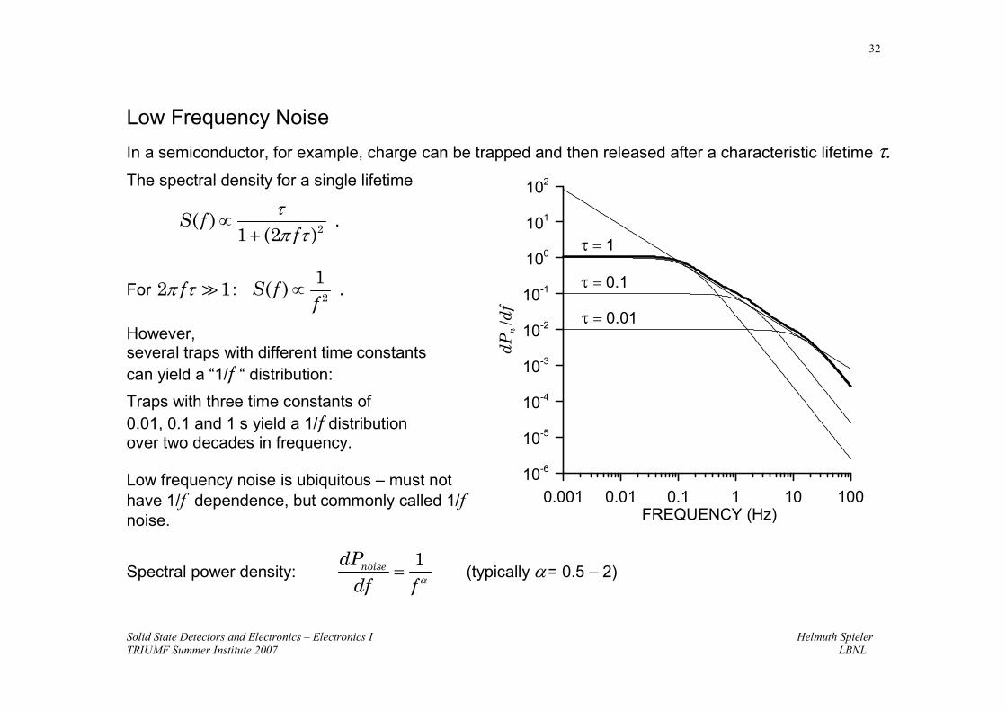
Low Frequency NoiseIn a semiconductor, for example, charge can be trapped and then released after a characteristic lifetime τ.The spectral density for a single lifetime
2( ) .1 (2 )
S ff
τπ τ
∝+
For 2 1fπ τ : 2
1( ) .S f
f∝
However,several traps with different time constantscan yield a “1/f “ distribution:Traps with three time constants of0.01, 0.1 and 1 s yield a 1/f distributionover two decades in frequency.
Low frequency noise is ubiquitous – must nothave 1/f dependence, but commonly called 1/fnoise.
Spectral power density:1noisedP
df f α= (typically α= 0.5 – 2)
0.001 0.01 0.1 1 10 100FREQUENCY (Hz)
10-6
10-5
10-4
10-3
10-2
10-1
100
101
102
dP
n/d
f
τ = 0.1
τ = 1
τ = 0.01
Solid State Detectors and Electronics – Electronics I Helmuth SpielerTRIUMF Summer Institute 2007 LBNL
33
4. Charge-Sensitive Amplifier – Noise vs. Detector Capacitance
In a voltage-sensitive preamplifier
• noise voltage at the output is essentially independent of detector capacitance,
i.e. the equivalent input noise voltage /ni no vv v A= .
• input signal decreases with increasing input capacitance, so signal-to-noise ratio depends ondetector capacitance.
In a charge-sensitive preamplifier, the signal at the amplifier output is independent of detectorcapacitance (if i dC C ).
What is the noise behavior?
• Noise appearing at the output of the preamplifier is fed back to the input, decreasing the outputnoise from the open-loop value no ni vv v A= .
• The magnitude of the feedback depends on the shunt impedance at the input, i.e. the detectorcapacitance.
Note, that although specified as an equivalent input noise, the dominant noise sources are typicallyinternal to the amplifier. Only in a fed-back configuration is some of this noise actually present atthe input. In other words, the primary noise signal is not a physical charge (or voltage) at theamplifier input, to which the loop responds in the same manner as to a detector signal.
⇒ S/N at the amplifier output depends on feedback.
Solid State Detectors and Electronics – Electronics I Helmuth SpielerTRIUMF Summer Institute 2007 LBNL
34
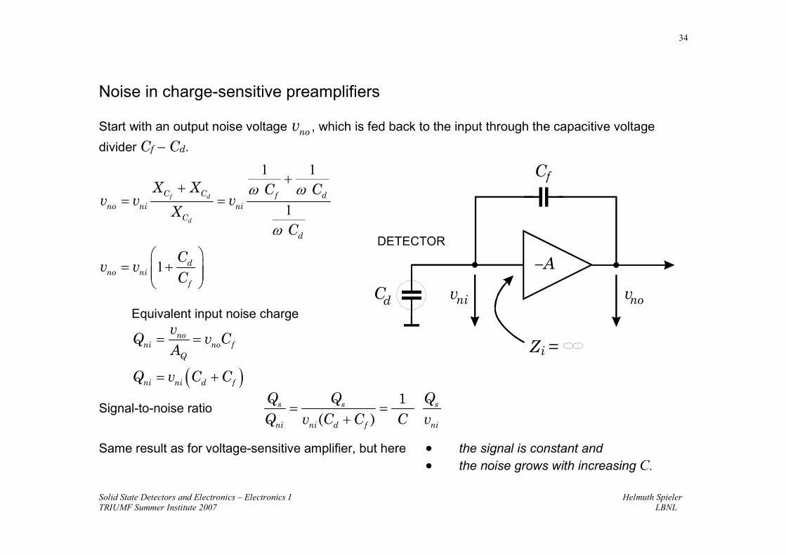
Noise in charge-sensitive preamplifiers
Start with an output noise voltage nov , which is fed back to the input through the capacitive voltagedivider Cf – Cd.
1 1
1
1
f d
d
C C f dno ni ni
C
d
dno ni
f
X X C Cv v v
XC
Cv v
C
ω ω
ω
++
= =
= +
Equivalent input noise charge
( )
noni no f
Q
ni ni d f
vQ v C
A
Q v C C
= =
= +
Signal-to-noise ratio1
( )s s s
ni ni d f ni
Q Q QQ v C C C v
= =+
Same result as for voltage-sensitive amplifier, but here • the signal is constant and• the noise grows with increasing C.
v v
C
A
C ni no
f
d
DETECTOR
Zi =
Solid State Detectors and Electronics – Electronics I Helmuth SpielerTRIUMF Summer Institute 2007 LBNL
35
As shown previously, the pulse rise time at the amplifier output alsoincreases with total capacitive input load C, because of reduced feedback.
In contrast, the rise time of a voltage sensitive amplifier is not affected by the inputcapacitance, although the equivalent noise charge increases with C just as for the charge-sensitive amplifier.
Conclusion
In general
• optimum S/N is independent of whether the voltage,current, or charge signal is sensed.
• S/N cannot be iimmpprroovveedd by feedback.
Practical considerations, i.e. type of detector, amplifier technology, can favor oneconfiguration over the other.
Solid State Detectors and Electronics – Electronics I Helmuth SpielerTRIUMF Summer Institute 2007 LBNL
36
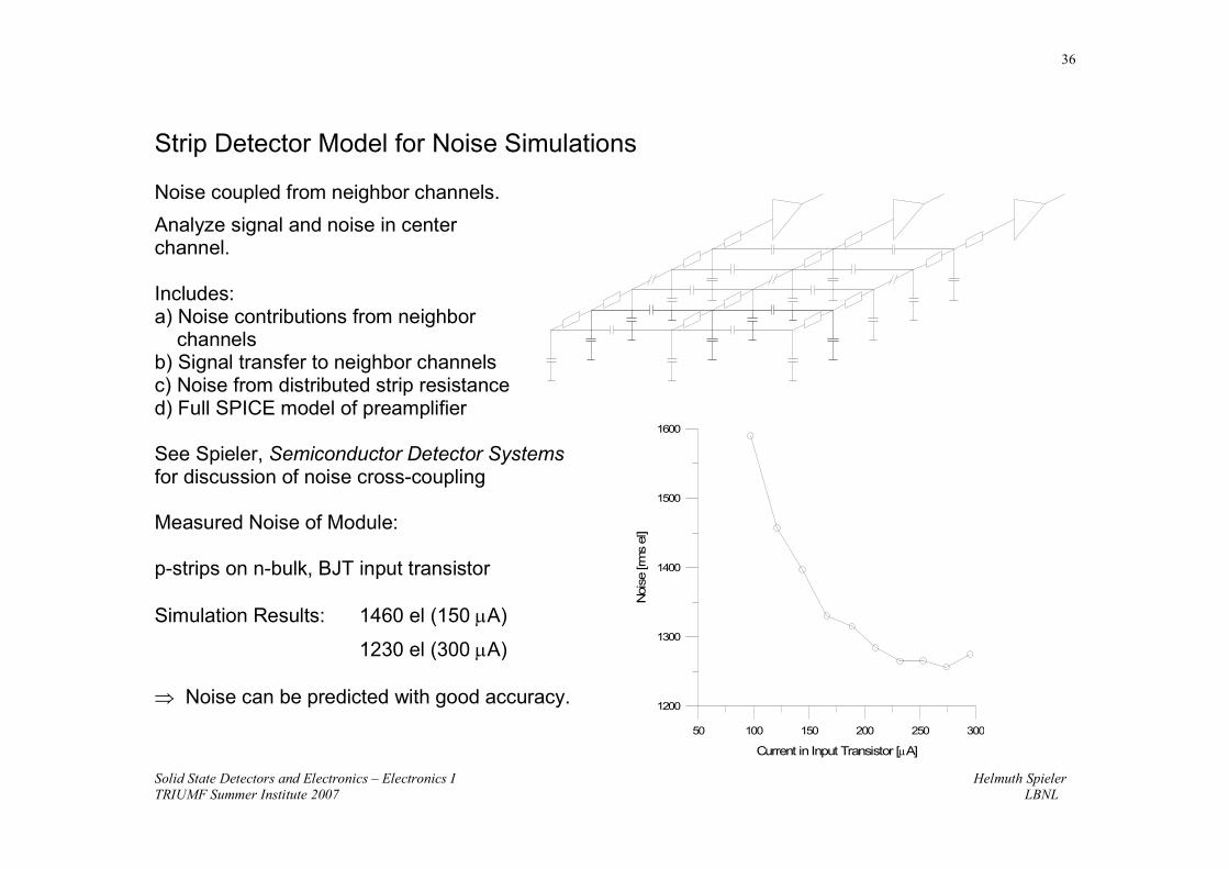
Strip Detector Model for Noise Simulations
Noise coupled from neighbor channels.Analyze signal and noise in centerchannel.
Includes:a) Noise contributions from neighbor
channelsb) Signal transfer to neighbor channelsc) Noise from distributed strip resistanced) Full SPICE model of preamplifier
See Spieler, Semiconductor Detector Systemsfor discussion of noise cross-coupling
Measured Noise of Module:
p-strips on n-bulk, BJT input transistor
Simulation Results: 1460 el (150 µA)
1230 el (300 µA)
⇒ Noise can be predicted with good accuracy.50 100 150 200 250 300
Current in Input Transistor [µA]
1200
1300
1400
1500
1600
Noi
se [r
ms
el]
Solid State Detectors and Electronics – Electronics I Helmuth SpielerTRIUMF Summer Institute 2007 LBNL
37
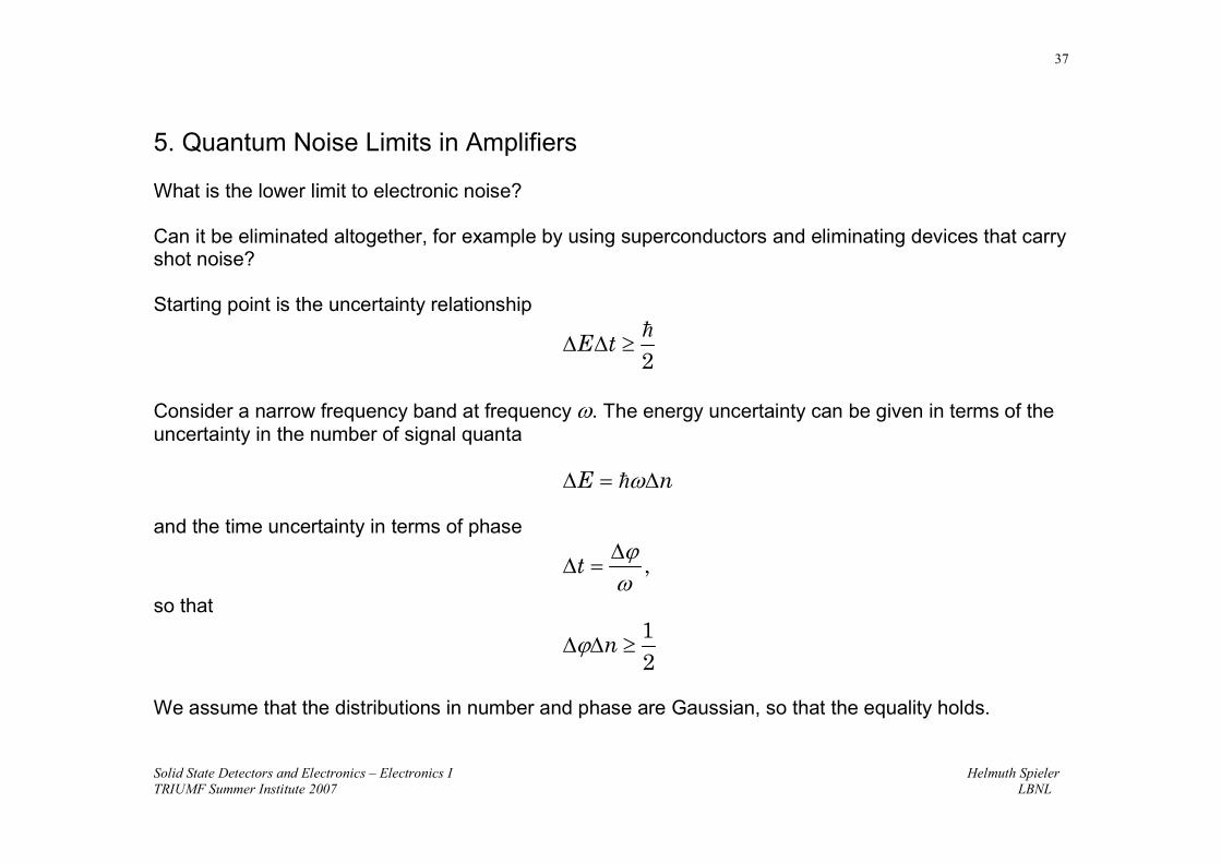
5. Quantum Noise Limits in Amplifiers
What is the lower limit to electronic noise?
Can it be eliminated altogether, for example by using superconductors and eliminating devices that carryshot noise?
Starting point is the uncertainty relationship
2E t∆ ∆ ≥
Consider a narrow frequency band at frequency ω. The energy uncertainty can be given in terms of theuncertainty in the number of signal quanta
E nω∆ = ∆
and the time uncertainty in terms of phase
,tϕω∆
∆ =
so that12
nϕ∆ ∆ ≥
We assume that the distributions in number and phase are Gaussian, so that the equality holds.
Solid State Detectors and Electronics – Electronics I Helmuth SpielerTRIUMF Summer Institute 2007 LBNL
38
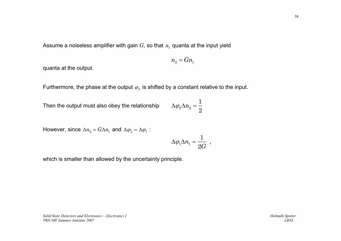
Assume a noiseless amplifier with gain G, so that 1n quanta at the input yield
2 1n Gn=quanta at the output.
Furthermore, the phase at the output ϕ2 is shifted by a constant relative to the input.
Then the output must also obey the relationship 2 2
12
nϕ∆ ∆ =
However, since ∆ = ∆2 1n G n and ϕ ϕ∆ = ∆2 1 :
1 1
1,
2n
Gϕ∆ ∆ =
which is smaller than allowed by the uncertainty principle.
Solid State Detectors and Electronics – Electronics I Helmuth SpielerTRIUMF Summer Institute 2007 LBNL
39
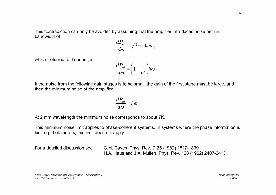
This contradiction can only be avoided by assuming that the amplifier introduces noise per unitbandwidth of
( 1) ,nodPG
dω
ω= −
which, referred to the input, is1
1nidPd G
ωω
= −
If the noise from the following gain stages is to be small, the gain of the first stage must be large, andthen the minimum noise of the amplifier
nidPd
ωω
=
At 2 mm wavelength the minimum noise corresponds to about 7K.
This minimum noise limit applies to phase-coherent systems. In systems where the phase information islost, e.g. bolometers, this limit does not apply.
For a detailed discussion see C.M. Caves, Phys. Rev. D 26 (1982) 1817-1839H.A. Haus and J.A. Mullen, Phys. Rev. 128 (1962) 2407-2413
Solid State Detectors and Electronics – Electronics I Helmuth SpielerTRIUMF Summer Institute 2007 LBNL
40
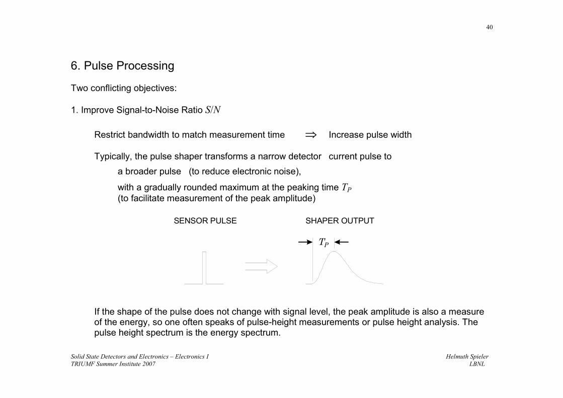
6. Pulse Processing
Two conflicting objectives:
1. Improve Signal-to-Noise Ratio S/N
Restrict bandwidth to match measurement time ⇒ Increase pulse width
Typically, the pulse shaper transforms a narrow detector current pulse toa broader pulse (to reduce electronic noise),
with a gradually rounded maximum at the peaking time TP(to facilitate measurement of the peak amplitude)
If the shape of the pulse does not change with signal level, the peak amplitude is also a measureof the energy, so one often speaks of pulse-height measurements or pulse height analysis. Thepulse height spectrum is the energy spectrum.
TP
SENSOR PULSE SHAPER OUTPUT

Solid State Detectors and Electronics – Electronics I Helmuth SpielerTRIUMF Summer Institute 2007 LBNL
41
2. Improve Pulse Pair Resolution ⇒ Decrease pulse width
Pulse pile-up distorts amplitude measurement. Reducing pulse shaping time to 1/3 eliminatespile-up.
Necessary to find balance between these conflicting requirements. Sometimes minimum noise iscrucial, sometimes rate capability is paramount.Usually, many considerations combined lead to a “non-textbook” compromise.
• “Optimum shaping” depends on the application!
• Shapers need not be complicated – Every amplifier is a pulse shaper!
TIME
AM
PLI
TUD
E
TIME
AM
PLI
TUD
E
Solid State Detectors and Electronics – Electronics I Helmuth SpielerTRIUMF Summer Institute 2007 LBNL
42
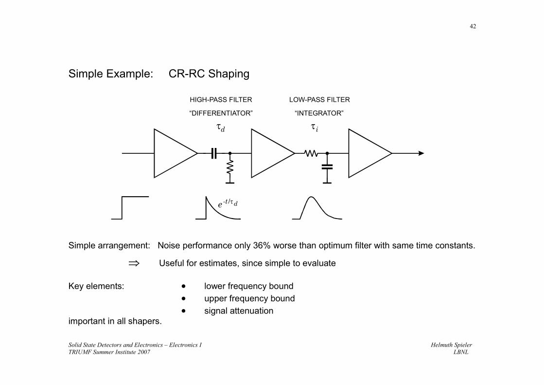
Simple Example: CR-RC Shaping
Simple arrangement: Noise performance only 36% worse than optimum filter with same time constants.
⇒ Useful for estimates, since simple to evaluate
Key elements: • lower frequency bound• upper frequency bound• signal attenuation
important in all shapers.
τ τd i
HIGH-PASS FILTER
“DIFFERENTIATOR”
LOW-PASS FILTER
“INTEGRATOR”
e-t /τd
Solid State Detectors and Electronics – Electronics I Helmuth SpielerTRIUMF Summer Institute 2007 LBNL
43
Pulse Shaping and Signal-to-Noise Ratio
Pulse shaping affects both the
• total noise
and
• peak signal amplitude
at the output of the shaper.
Equivalent Noise Charge
Inject known signal charge into preamp input(either via test input or known energy in detector).
Determine signal-to-noise ratio at shaper output.
Equivalent Noise Charge ≡ Input charge for which S/N = 1
Solid State Detectors and Electronics – Electronics I Helmuth SpielerTRIUMF Summer Institute 2007 LBNL
44
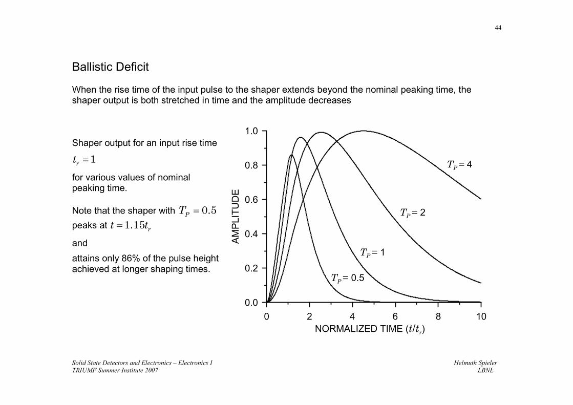
Ballistic Deficit
When the rise time of the input pulse to the shaper extends beyond the nominal peaking time, theshaper output is both stretched in time and the amplitude decreases
Shaper output for an input rise time
1rt =
for various values of nominalpeaking time.
Note that the shaper with 0.5PT =peaks at 1.15 rt t=
andattains only 86% of the pulse heightachieved at longer shaping times.
0 2 4 6 8 10NORMALIZED TIME (t/tr)
0.0
0.2
0.4
0.6
0.8
1.0
AM
PLIT
UD
E
TP = 0.5
TP = 1
TP = 2
TP = 4
Solid State Detectors and Electronics – Electronics I Helmuth SpielerTRIUMF Summer Institute 2007 LBNL
45
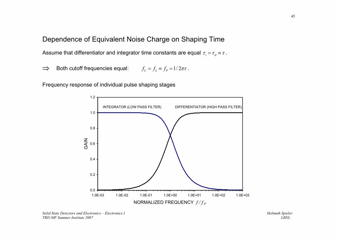
Dependence of Equivalent Noise Charge on Shaping Time
Assume that differentiator and integrator time constants are equal τ τ τ= ≡i d .
⇒ Both cutoff frequencies equal: 1/ 2πτ= ≡ =U L Pf f f .
Frequency response of individual pulse shaping stages
0.0
0.2
0.4
0.6
0.8
1.0
1.2
1.0E-03 1.0E-02 1.0E-01 1.0E+00 1.0E+01 1.0E+02 1.0E+03
NORMALIZED FREQUENCY f / f P
GA
IN
INTEGRATOR (LOW PASS FILTER) DIFFERENTIATOR (HIGH PASS FILTER)
Solid State Detectors and Electronics – Electronics I Helmuth SpielerTRIUMF Summer Institute 2007 LBNL
46
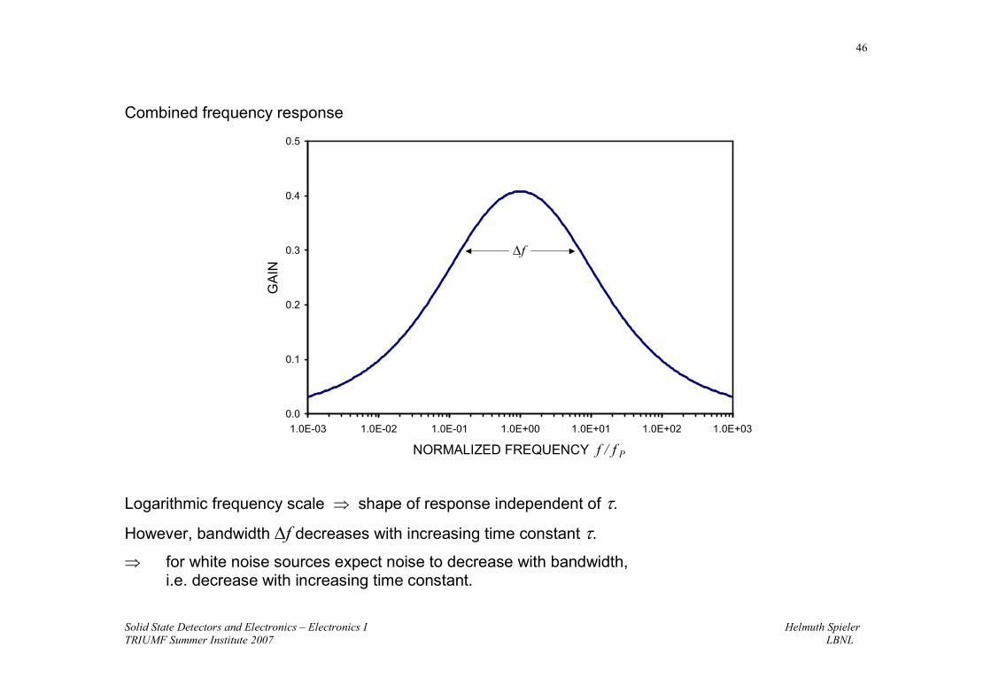
Combined frequency response
Logarithmic frequency scale ⇒ shape of response independent of τ.
However, bandwidth ∆f decreases with increasing time constant τ.⇒ for white noise sources expect noise to decrease with bandwidth,
i.e. decrease with increasing time constant.
0.0
0.1
0.2
0.3
0.4
0.5
1.0E-03 1.0E-02 1.0E-01 1.0E+00 1.0E+01 1.0E+02 1.0E+03
NORMALIZED FREQUENCY f / f P
GAI
N
∆f
Solid State Detectors and Electronics – Electronics I Helmuth SpielerTRIUMF Summer Institute 2007 LBNL
47
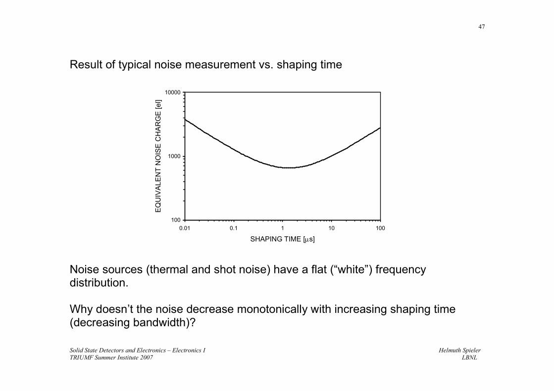
Result of typical noise measurement vs. shaping time
Noise sources (thermal and shot noise) have a flat (“white”) frequencydistribution.
Why doesn’t the noise decrease monotonically with increasing shaping time(decreasing bandwidth)?
100
1000
10000
0.01 0.1 1 10 100
SHAPING TIME [µs]
EQ
UIV
ALE
NT
NO
ISE
CH
AR
GE
[el]
Solid State Detectors and Electronics – Electronics I Helmuth SpielerTRIUMF Summer Institute 2007 LBNL
48
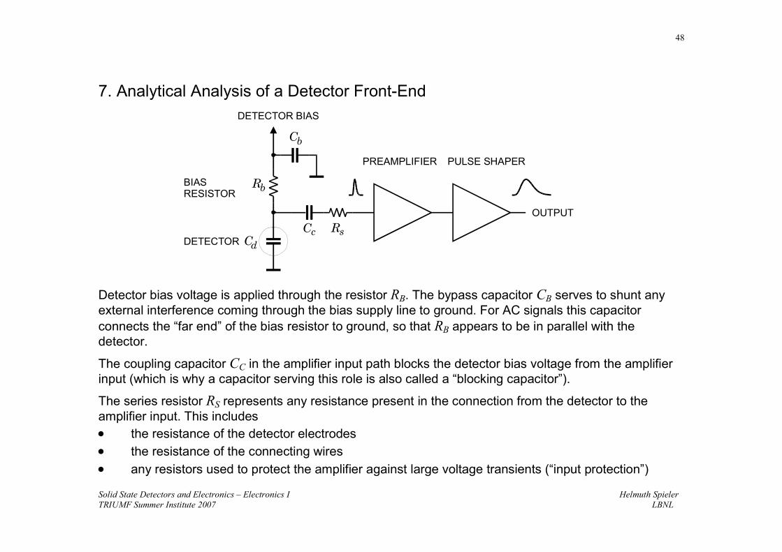
7. Analytical Analysis of a Detector Front-End
Detector bias voltage is applied through the resistor RB. The bypass capacitor CB serves to shunt anyexternal interference coming through the bias supply line to ground. For AC signals this capacitorconnects the “far end” of the bias resistor to ground, so that RB appears to be in parallel with thedetector.
The coupling capacitor CC in the amplifier input path blocks the detector bias voltage from the amplifierinput (which is why a capacitor serving this role is also called a “blocking capacitor”).
The series resistor RS represents any resistance present in the connection from the detector to theamplifier input. This includes• the resistance of the detector electrodes• the resistance of the connecting wires• any resistors used to protect the amplifier against large voltage transients (“input protection”)
OUTPUT
DETECTOR
BIASRESISTOR
Rb
Cc Rs
Cb
Cd
DETECTOR BIAS
PULSE SHAPERPREAMPLIFIER
Solid State Detectors and Electronics – Electronics I Helmuth SpielerTRIUMF Summer Institute 2007 LBNL
49
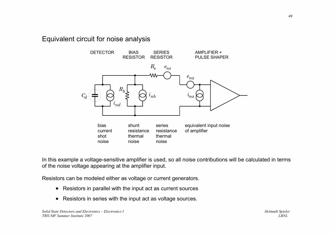
Equivalent circuit for noise analysis
bias shunt series equivalent input noisecurrent resistance resistance of amplifiershot thermal thermalnoise noise noise
In this example a voltage-sensitive amplifier is used, so all noise contributions will be calculated in termsof the noise voltage appearing at the amplifier input.
Resistors can be modeled either as voltage or current generators.
• Resistors in parallel with the input act as current sources
• Resistors in series with the input act as voltage sources.
DETECTOR
Cd
BIASRESISTOR
SERIESRESISTOR
AMPLIFIER +PULSE SHAPER
Rb
Rs
i
i i
e
e
nd
nb na
ns
na
Solid State Detectors and Electronics – Electronics I Helmuth SpielerTRIUMF Summer Institute 2007 LBNL
50
Steps in the analysis:
1. Determine the frequency distribution of the noise voltage presented to the amplifierinput from all individual noise sources
2. Integrate over the frequency response of a CR-RC shaper to determine the totalnoise output.
3. Determine the output signal for a known signal charge and calculate equivalentnoise charge (signal charge for S/N= 1)
First, assume a simple CR-RC shaper with
equal differentiation and integration time constants τd = τi = τ ,
which in this special case is equal to the peaking time.
Solid State Detectors and Electronics – Electronics I Helmuth SpielerTRIUMF Summer Institute 2007 LBNL
51
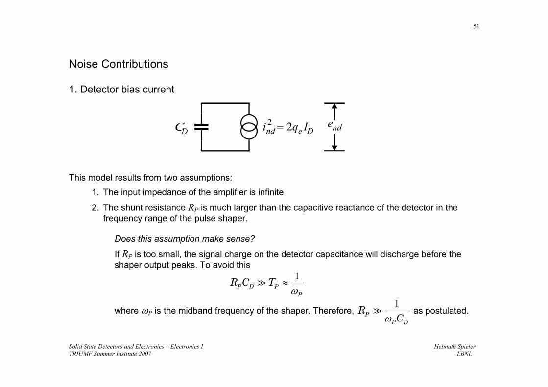
Noise Contributions
1. Detector bias current
This model results from two assumptions:1. The input impedance of the amplifier is infinite
2. The shunt resistance RP is much larger than the capacitive reactance of the detector in thefrequency range of the pulse shaper.
Does this assumption make sense?
If RP is too small, the signal charge on the detector capacitance will discharge before theshaper output peaks. To avoid this
1P D P
P
R C Tω
≈
where ωP is the midband frequency of the shaper. Therefore,1
PP D
RCω
as postulated.
CDend2qe DIind
2 =
Solid State Detectors and Electronics – Electronics I Helmuth SpielerTRIUMF Summer Institute 2007 LBNL
52
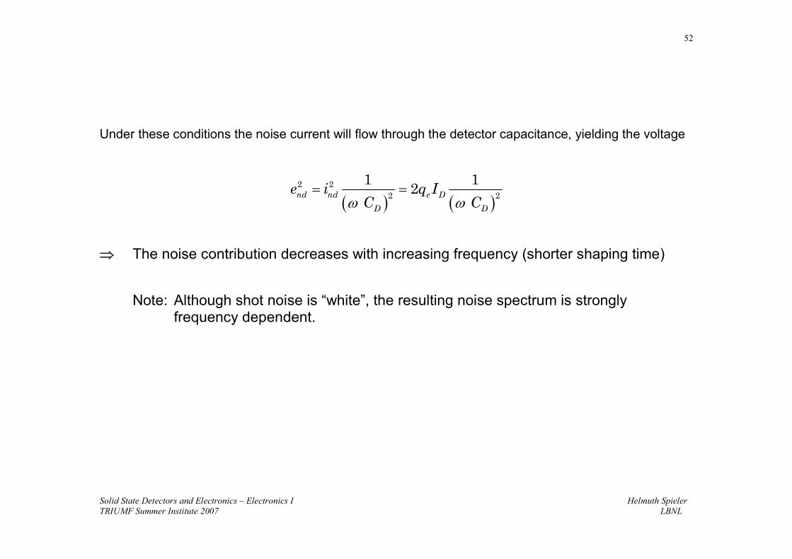
Under these conditions the noise current will flow through the detector capacitance, yielding the voltage
( ) ( )2 2
2 2
1 12nd nd e D
D D
e i q IC Cω ω
= =
⇒ The noise contribution decreases with increasing frequency (shorter shaping time)
Note: Although shot noise is “white”, the resulting noise spectrum is stronglyfrequency dependent.
Solid State Detectors and Electronics – Electronics I Helmuth SpielerTRIUMF Summer Institute 2007 LBNL
53
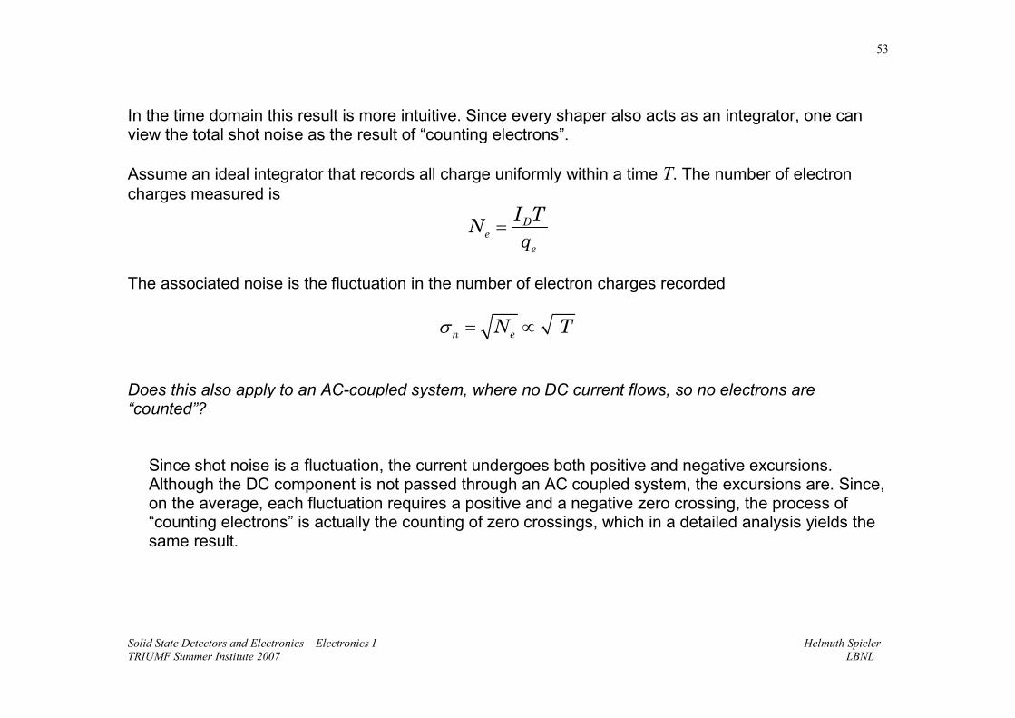
In the time domain this result is more intuitive. Since every shaper also acts as an integrator, one canview the total shot noise as the result of “counting electrons”.
Assume an ideal integrator that records all charge uniformly within a time T. The number of electroncharges measured is
De
e
I TN
q=
The associated noise is the fluctuation in the number of electron charges recorded
n eN Tσ = ∝
Does this also apply to an AC-coupled system, where no DC current flows, so no electrons are“counted”?
Since shot noise is a fluctuation, the current undergoes both positive and negative excursions.Although the DC component is not passed through an AC coupled system, the excursions are. Since,on the average, each fluctuation requires a positive and a negative zero crossing, the process of“counting electrons” is actually the counting of zero crossings, which in a detailed analysis yields thesame result.
Solid State Detectors and Electronics – Electronics I Helmuth SpielerTRIUMF Summer Institute 2007 LBNL
54
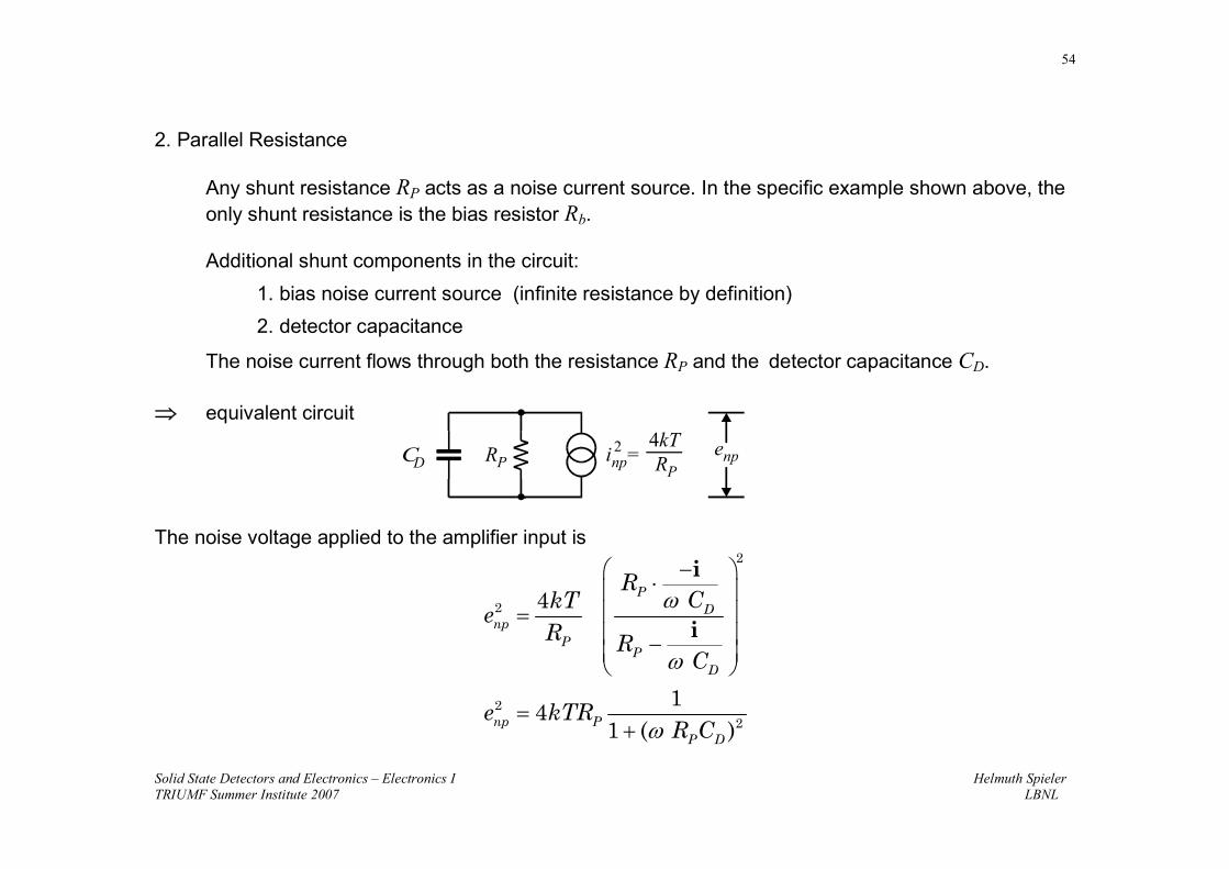
2. Parallel Resistance
Any shunt resistance RP acts as a noise current source. In the specific example shown above, theonly shunt resistance is the bias resistor Rb.
Additional shunt components in the circuit:1. bias noise current source (infinite resistance by definition)2. detector capacitance
The noise current flows through both the resistance RP and the detector capacitance CD.
⇒ equivalent circuit
The noise voltage applied to the amplifier input is2
2
22
4
14
1 ( )
PD
npP
PD
np PP D
RCkT
eR R
C
e kTRR C
ω
ω
ω
− ⋅ = −
=+
i
i
CD R RP P
4kT enpinp2 =
Solid State Detectors and Electronics – Electronics I Helmuth SpielerTRIUMF Summer Institute 2007 LBNL
55
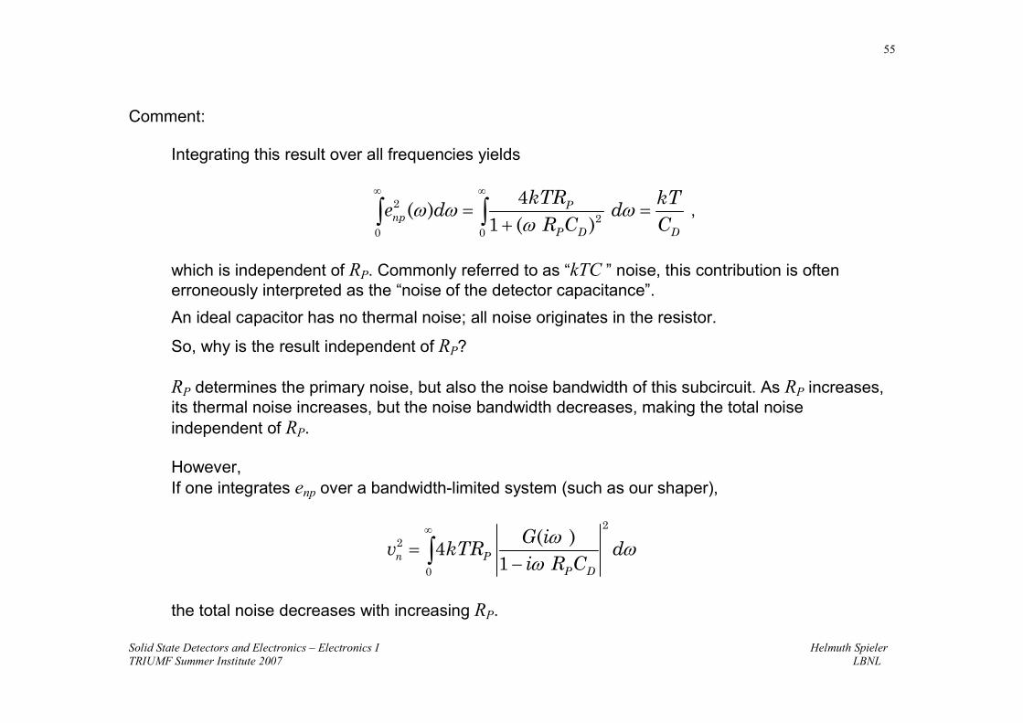
Comment:
Integrating this result over all frequencies yields
22
0 0
4( )
1 ( )P
npP D D
kTR kTe d d
R C Cω ω ω
ω
∞ ∞
= =+∫ ∫ ,
which is independent of RP. Commonly referred to as “kTC ” noise, this contribution is oftenerroneously interpreted as the “noise of the detector capacitance”.An ideal capacitor has no thermal noise; all noise originates in the resistor.
So, why is the result independent of RP?
RP determines the primary noise, but also the noise bandwidth of this subcircuit. As RP increases,its thermal noise increases, but the noise bandwidth decreases, making the total noiseindependent of RP.
However,If one integrates enp over a bandwidth-limited system (such as our shaper),
2
2
0
( )4
1n PP D
G iv kTR d
i R Cω ω
ω
∞
=−∫
the total noise decreases with increasing RP.

Solid State Detectors and Electronics – Electronics I Helmuth SpielerTRIUMF Summer Institute 2007 LBNL
56
3. Series Resistance
The noise voltage generator associated with the series resistance RS is in series with the othernoise sources, so it simply contributes
2 4nr Se kTR=
Solid State Detectors and Electronics – Electronics I Helmuth SpielerTRIUMF Summer Institute 2007 LBNL
57
4. Amplifier input noise
The amplifier noise voltage sources usually are not physically present at the amplifier input.Instead the amplifier noise originates within the amplifier, appears at the output, and is referred tothe input by dividing the output noise by the amplifier gain, where it appears as a noise voltagegenerator.
2 2 fna nw
Ae e
f= +
↑ ↑“white noise” 1/f noise (can also originate in external components)
This noise voltage generator also adds in series with the other sources.
• Amplifiers generally also exhibit input current noise, which is physically present at the input. Itseffect is the same as for the detector bias current, so the analysis given in 1. can be applied.
• In a well-designed amplifier the noise is dominated by the input transistor (fast, high-gaintransistors generally best). Noise parameters of transistors are discussed in the Appendix.Transistor input noise decreases with transconductance
⇒ increased power• Minimum device noise limited both by technology and fundamental physics.
Solid State Detectors and Electronics – Electronics I Helmuth SpielerTRIUMF Summer Institute 2007 LBNL
58
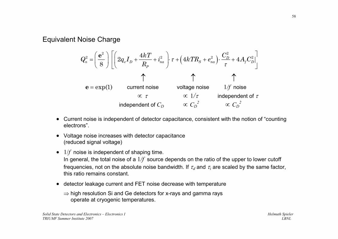
Equivalent Noise Charge
( )22
2 2 2 242 4 4
8D
n e D na S na f DP
CkTQ q I i kTR e A C
Rτ
τ
= + + ⋅ + + ⋅ +
e
↑ ↑ ↑exp(1)=e current noise voltage noise 1/f noise
∝ τ ∝ 1/τ independent of τindependent of CD ∝ CD
2 ∝ CD2
• Current noise is independent of detector capacitance, consistent with the notion of “countingelectrons”.
• Voltage noise increases with detector capacitance(reduced signal voltage)
• 1/f noise is independent of shaping time.In general, the total noise of a 1/f source depends on the ratio of the upper to lower cutofffrequencies, not on the absolute noise bandwidth. If τd and τi are scaled by the same factor,this ratio remains constant.
• detector leakage current and FET noise decrease with temperature
⇒ high resolution Si and Ge detectors for x-rays and gamma raysoperate at cryogenic temperatures.
Solid State Detectors and Electronics – Electronics I Helmuth SpielerTRIUMF Summer Institute 2007 LBNL
59
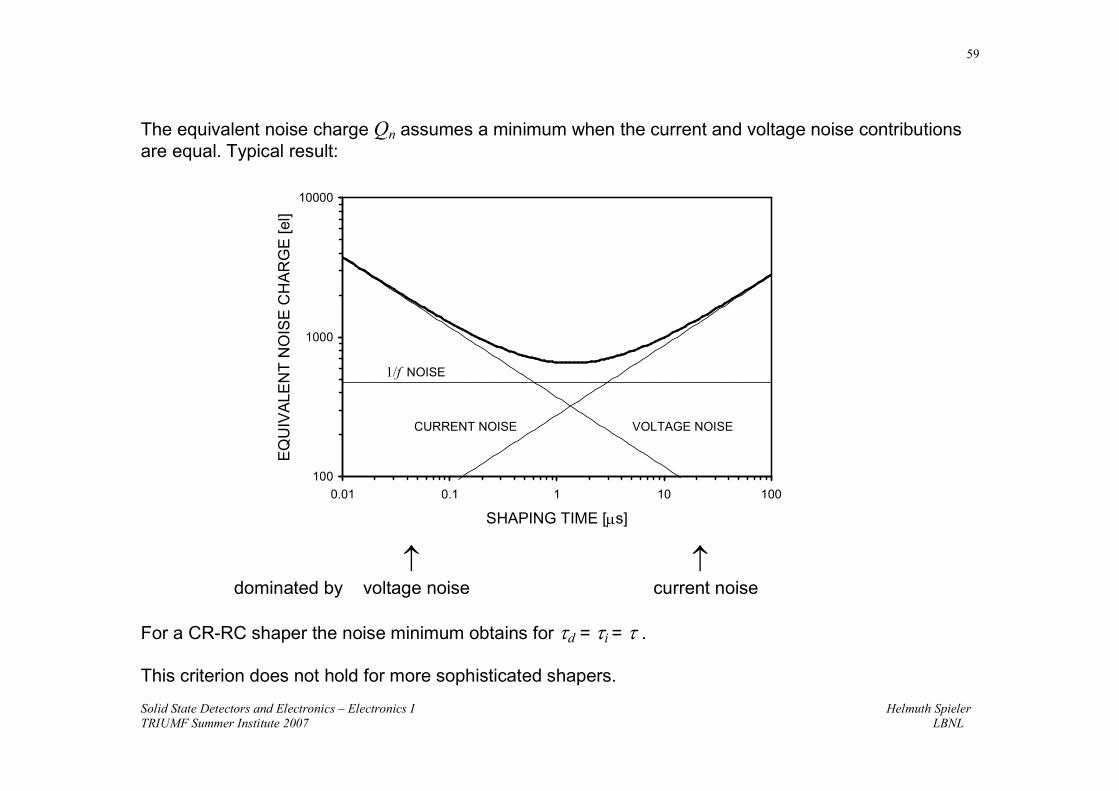
The equivalent noise charge Qn assumes a minimum when the current and voltage noise contributionsare equal. Typical result:
↑ ↑dominated by voltage noise current noise
For a CR-RC shaper the noise minimum obtains for τd = τi = τ .
This criterion does not hold for more sophisticated shapers.
100
1000
10000
0.01 0.1 1 10 100
SHAPING TIME [µs]
EQU
IVA
LEN
T N
OIS
E C
HA
RG
E [e
l]
VOLTAGE NOISE
1/f NOISE
CURRENT NOISE
Solid State Detectors and Electronics – Electronics I Helmuth SpielerTRIUMF Summer Institute 2007 LBNL
60
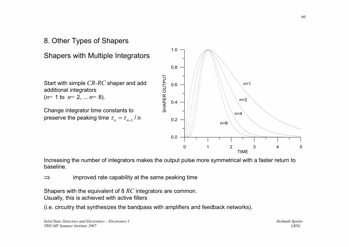
8. Other Types of Shapers
Shapers with Multiple Integrators
Start with simple CR-RC shaper and addadditional integrators(n= 1 to n= 2, ... n= 8).
Change integrator time constants topreserve the peaking time 1 /n n nτ τ ==
Increasing the number of integrators makes the output pulse more symmetrical with a faster return tobaseline.
⇒ improved rate capability at the same peaking time
Shapers with the equivalent of 8 RC integrators are common.Usually, this is achieved with active filters(i.e. circuitry that synthesizes the bandpass with amplifiers and feedback networks).
0 1 2 3 4 5TIME
0.0
0.2
0.4
0.6
0.8
1.0
SH
AP
ER
OU
TPU
T
n=8
n=1
n=2
n=4
Solid State Detectors and Electronics – Electronics I Helmuth SpielerTRIUMF Summer Institute 2007 LBNL
61
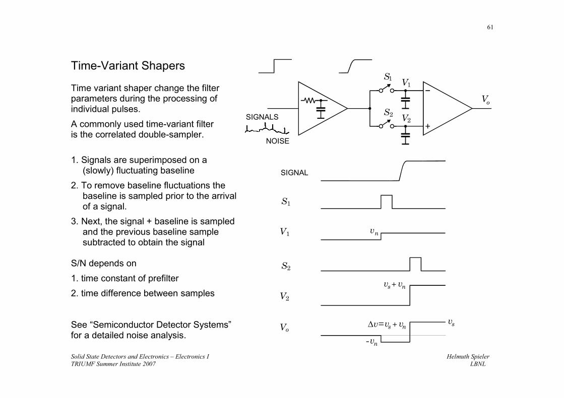
Time-Variant Shapers
Time variant shaper change the filterparameters during the processing ofindividual pulses.A commonly used time-variant filteris the correlated double-sampler.
1. Signals are superimposed on a(slowly) fluctuating baseline
2. To remove baseline fluctuations thebaseline is sampled prior to the arrivalof a signal.
3. Next, the signal + baseline is sampledand the previous baseline samplesubtracted to obtain the signal
S/N depends on1. time constant of prefilter2. time difference between samples
See “Semiconductor Detector Systems”for a detailed noise analysis.
SIGNALS
NOISE
S
S
S
S
V
V
V
V
V
Vo
SIGNAL
v
v
v
v v
v
v
n
n
s
s s
n
n
+
+∆v=
1
1
2
2
1
1
2
o
2
Solid State Detectors and Electronics – Electronics I Helmuth SpielerTRIUMF Summer Institute 2007 LBNL
62

Solid State Detectors and Electronics – Electronics I Helmuth SpielerTRIUMF Summer Institute 2007 LBNL
63
9. Examples: Photodiode Readout(S. Holland, N. Wang, I. Kipnis, B. Krieger, W. Moses, LBNL)
Medical Imaging (Positron Emission Tomography)
Read out 64 BGO crystals with one PMT (timing, energy) and tag crystal bysegmented photodiode array.
Solid State Detectors and Electronics – Electronics I Helmuth SpielerTRIUMF Summer Institute 2007 LBNL
64
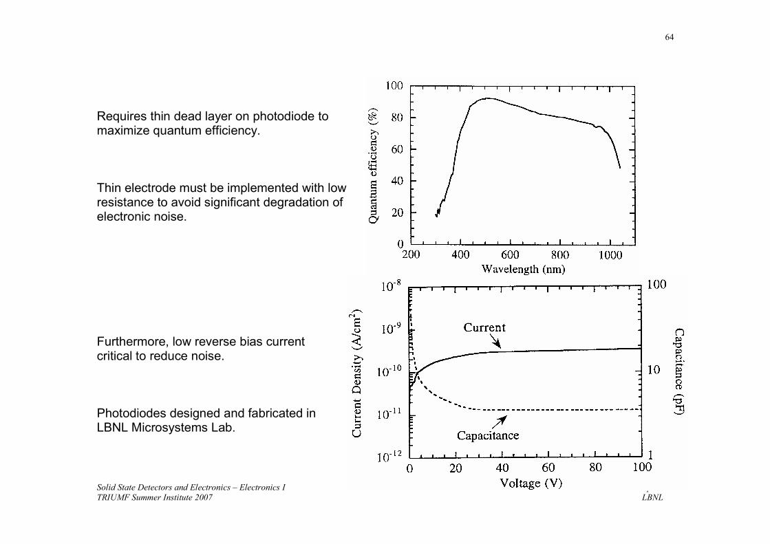
Requires thin dead layer on photodiode tomaximize quantum efficiency.
Thin electrode must be implemented with lowresistance to avoid significant degradation ofelectronic noise.
Furthermore, low reverse bias currentcritical to reduce noise.
Photodiodes designed and fabricated inLBNL Microsystems Lab.
Solid State Detectors and Electronics – Electronics I Helmuth SpielerTRIUMF Summer Institute 2007 LBNL
65
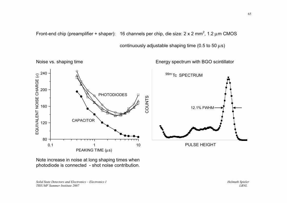
Front-end chip (preamplifier + shaper): 16 channels per chip, die size: 2 x 2 mm2, 1.2 µm CMOS
continuously adjustable shaping time (0.5 to 50 µs)
Noise vs. shaping time Energy spectrum with BGO scintillator
Note increase in noise at long shaping times whenphotodiode is connected - shot noise contribution.
0.1 1 10PEAKING TIME (µs)
80
120
160
200
240
EQ
UIV
ALEN
T N
OIS
E C
HA
RG
E (e
)
CAPACITOR
PHOTODIODES
Tc SPECTRUM99m
PULSE HEIGHTC
OU
NTS
12.1% FWHM
Solid State Detectors and Electronics – Electronics I Helmuth SpielerTRIUMF Summer Institute 2007 LBNL
66
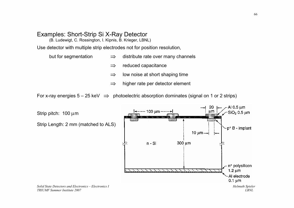
Examples: Short-Strip Si X-Ray Detector(B. Ludewigt, C. Rossington, I. Kipnis, B. Krieger, LBNL)
Use detector with multiple strip electrodes not for position resolution,
but for segmentation ⇒ distribute rate over many channels
⇒ reduced capacitance
⇒ low noise at short shaping time
⇒ higher rate per detector element
For x-ray energies 5 – 25 keV ⇒ photoelectric absorption dominates (signal on 1 or 2 strips)
Strip pitch: 100 µm
Strip Length: 2 mm (matched to ALS)
Solid State Detectors and Electronics – Electronics I Helmuth SpielerTRIUMF Summer Institute 2007 LBNL
67
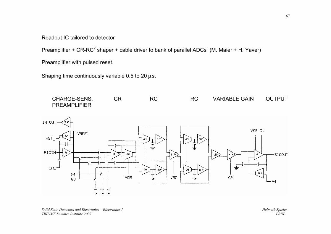
Readout IC tailored to detector
Preamplifier + CR-RC2 shaper + cable driver to bank of parallel ADCs (M. Maier + H. Yaver)
Preamplifier with pulsed reset.
Shaping time continuously variable 0.5 to 20 µs.
CHARGE-SENS. CR RC RC VARIABLE GAIN OUTPUTPREAMPLIFIER
Solid State Detectors and Electronics – Electronics I Helmuth SpielerTRIUMF Summer Institute 2007 LBNL
68
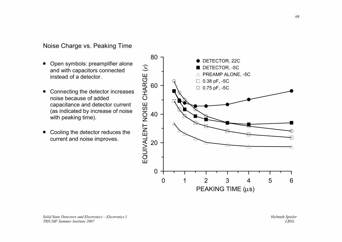
Noise Charge vs. Peaking Time
• Open symbols: preamplifier aloneand with capacitors connectedinstead of a detector.
• Connecting the detector increasesnoise because of addedcapacitance and detector current(as indicated by increase of noisewith peaking time).
• Cooling the detector reduces thecurrent and noise improves.
0 1 2 3 4 5 6PEAKING TIME (µs)
0
20
40
60
80
EQ
UIV
ALE
NT
NO
ISE
CH
AR
GE
(e)
DETECTOR, 22CDETECTOR, -5CPREAMP ALONE, -5C0.38 pF, -5C0.75 pF, -5C
Solid State Detectors and Electronics – Electronics I Helmuth SpielerTRIUMF Summer Institute 2007 LBNL
69
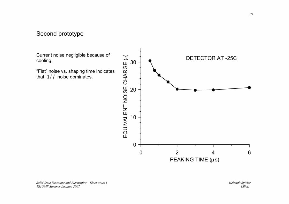
Second prototype
Current noise negligible because ofcooling.
“Flat” noise vs. shaping time indicatesthat 1/ f noise dominates.
0 2 4 6PEAKING TIME (µs)
0
10
20
30
EQ
UIV
ALE
NT
NO
ISE
CH
ARG
E (e
)
DETECTOR AT -25C
Solid State Detectors and Electronics – Electronics I Helmuth SpielerTRIUMF Summer Institute 2007 LBNL
70
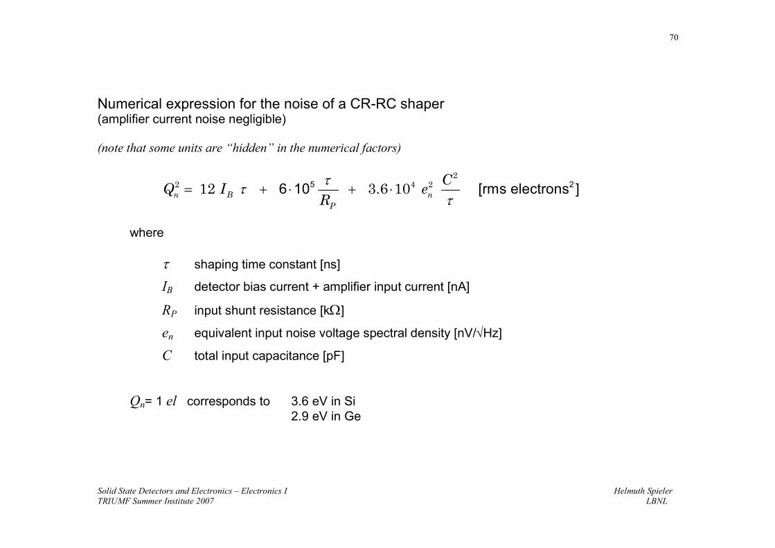
Numerical expression for the noise of a CR-RC shaper(amplifier current noise negligible)
(note that some units are “hidden” in the numerical factors)
5 26 10 [rms electrons ]2
2 4 212 3.6 10n B nP
CQ I e
Rττ
τ= + ⋅ + ⋅
where
τ shaping time constant [ns]
IB detector bias current + amplifier input current [nA]
RP input shunt resistance [kΩ]
en equivalent input noise voltage spectral density [nV/√Hz]
C total input capacitance [pF]
Qn= 1 el corresponds to 3.6 eV in Si2.9 eV in Ge

Solid State Detectors and Electronics – Electronics I Helmuth SpielerTRIUMF Summer Institute 2007 LBNL
71
“Series” and “Parallel” Noise
For sources connected in parallel, currents are additive.
For sources connected in series, voltages are additive.
⇒ In the detector community voltage and current noise are oftencalled “series” and “parallel” noise.
The rest of the world uses equivalent noise voltage and current.
Since they are physically meaningful, use of these widely understood terms ispreferable.
Solid State Detectors and Electronics – Electronics I Helmuth SpielerTRIUMF Summer Institute 2007 LBNL
72
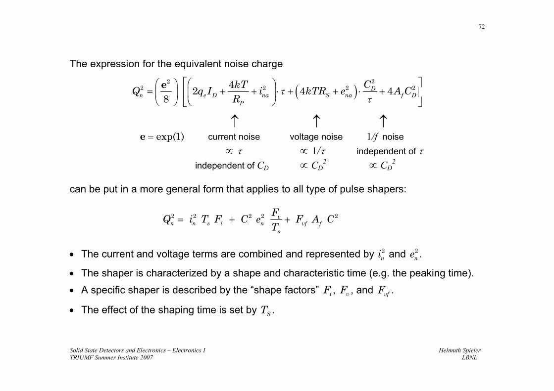
The expression for the equivalent noise charge
( )22
2 2 2 242 4 4
8D
n e D na S na f DP
CkTQ q I i kTR e A C
Rτ
τ
= + + ⋅ + + ⋅ +
e
↑ ↑ ↑exp(1)=e current noise voltage noise 1/f noise
∝ τ ∝ 1/τ independent of τindependent of CD ∝ CD
2 ∝ CD2
can be put in a more general form that applies to all type of pulse shapers:
2 2 2 2 2vn n s i n vf f
s
FQ i T F C e F A C
T= + +
• The current and voltage terms are combined and represented by 2ni and 2
ne .
• The shaper is characterized by a shape and characteristic time (e.g. the peaking time).• A specific shaper is described by the “shape factors” iF , vF , and vfF .
• The effect of the shaping time is set by ST .
Solid State Detectors and Electronics – Electronics I Helmuth SpielerTRIUMF Summer Institute 2007 LBNL
73
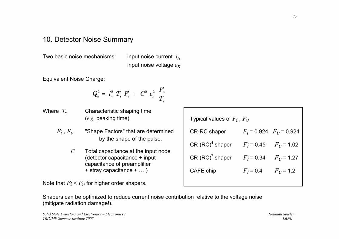
10. Detector Noise Summary
Two basic noise mechanisms: input noise current ininput noise voltage en
Equivalent Noise Charge:
Where Ts Characteristic shaping time(e.g. peaking time)
Fi , Fv "Shape Factors" that are determinedby the shape of the pulse.
C Total capacitance at the input node(detector capacitance + inputcapacitance of preamplifier+ stray capacitance + … )
Note that Fi < Fv for higher order shapers.
Shapers can be optimized to reduce current noise contribution relative to the voltage noise(mitigate radiation damage!).
2 2 2 2 vn n s i n
s
FQ i T F C e
T= +
Typical values of Fi , Fv
CR-RC shaper Fi = 0.924 Fv = 0.924
CR-(RC)4 shaper Fi = 0.45 Fv = 1.02
CR-(RC)7 shaper Fi = 0.34 Fv = 1.27
CAFE chip Fi = 0.4 Fv = 1.2
Solid State Detectors and Electronics – Electronics I Helmuth SpielerTRIUMF Summer Institute 2007 LBNL
74
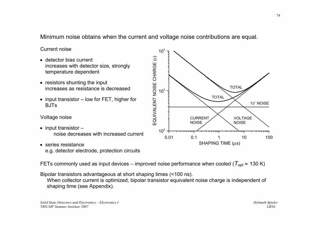
Minimum noise obtains when the current and voltage noise contributions are equal.
Current noise
• detector bias currentincreases with detector size, stronglytemperature dependent
• resistors shunting the inputincreases as resistance is decreased
• input transistor – low for FET, higher forBJTs
Voltage noise
• input transistor –noise decreases with increased current
• series resistancee.g. detector electrode, protection circuits
FETs commonly used as input devices – improved noise performance when cooled (Topt ≈ 130 K)
Bipolar transistors advantageous at short shaping times (<100 ns).When collector current is optimized, bipolar transistor equivalent noise charge is independent ofshaping time (see Appendix).
0.01 0.1 1 10 100SHAPING TIME (µs)
102
103
104
EQ
UIV
ALE
NT
NO
ISE
CH
AR
GE
(e)
CURRENTNOISE
VOLTAGENOISE
TOTAL1/f NOISE
TOTAL
Solid State Detectors and Electronics – Electronics I Helmuth SpielerTRIUMF Summer Institute 2007 LBNL
75
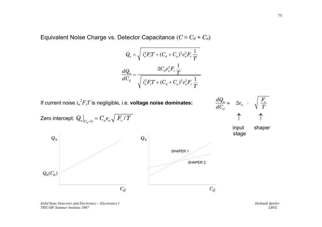
Equivalent Noise Charge vs. Detector Capacitance (C = Cd + Ca)
2 2 2
2
2 2 2
1( )
12
1( )
n n i d a n v
d n vn
dn i d a n v
Q i FT C C e FT
C e FdQ TdC
i FT C C e FT
= + +
=+ +
If current noise in2FiT is negligible, i.e. voltage noise dominates: 2n v
nd
dQ Fe
dC T≈ ⋅
Zero intercept:0
/d
n a n vCQ C e F T
== ↑ ↑
input shaperstage
Q
Q Q
C C
n
n n
d d
( )Ca
SHAPER 1
SHAPER 2
Solid State Detectors and Electronics – Electronics I Helmuth SpielerTRIUMF Summer Institute 2007 LBNL
76
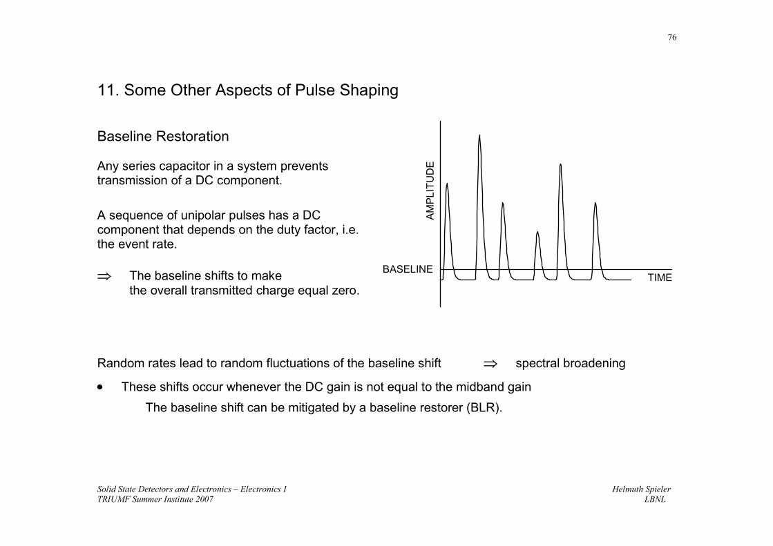
11. Some Other Aspects of Pulse Shaping
Baseline Restoration
Any series capacitor in a system preventstransmission of a DC component.
A sequence of unipolar pulses has a DCcomponent that depends on the duty factor, i.e.the event rate.
⇒ The baseline shifts to makethe overall transmitted charge equal zero.
Random rates lead to random fluctuations of the baseline shift ⇒ spectral broadening
• These shifts occur whenever the DC gain is not equal to the midband gainThe baseline shift can be mitigated by a baseline restorer (BLR).
AM
PLIT
UD
E
TIMEBASELINE
Solid State Detectors and Electronics – Electronics I Helmuth SpielerTRIUMF Summer Institute 2007 LBNL
77
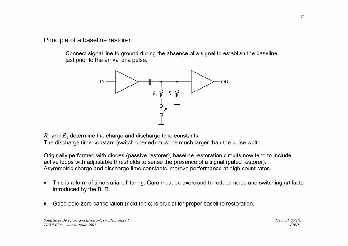
Principle of a baseline restorer:
Connect signal line to ground during the absence of a signal to establish the baselinejust prior to the arrival of a pulse.
R1 and R2 determine the charge and discharge time constants.The discharge time constant (switch opened) must be much larger than the pulse width.
Originally performed with diodes (passive restorer), baseline restoration circuits now tend to includeactive loops with adjustable thresholds to sense the presence of a signal (gated restorer).Asymmetric charge and discharge time constants improve performance at high count rates.
• This is a form of time-variant filtering. Care must be exercised to reduce noise and switching artifactsintroduced by the BLR.
• Good pole-zero cancellation (next topic) is crucial for proper baseline restoration.
IN OUT
R R1 2
Solid State Detectors and Electronics – Electronics I Helmuth SpielerTRIUMF Summer Institute 2007 LBNL
78
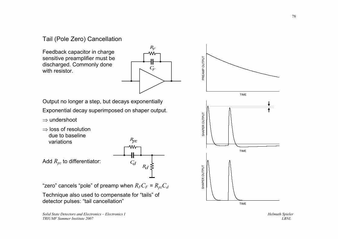
Tail (Pole Zero) Cancellation
Feedback capacitor in chargesensitive preamplifier must bedischarged. Commonly donewith resistor.
Output no longer a step, but decays exponentiallyExponential decay superimposed on shaper output.
⇒ undershoot
⇒ loss of resolutiondue to baselinevariations
Add Rpz to differentiator:
“zero” cancels “pole” of preamp when RFCF = RpzCd
Technique also used to compensate for “tails” ofdetector pulses: “tail cancellation”
TIME
SH
APE
R O
UTP
UT
TIMES
HA
PE
R O
UTP
UT
Cd Rd
Rpz
CF
RF
TIME
PR
EA
MP
OU
TPU
T
Solid State Detectors and Electronics – Electronics I Helmuth SpielerTRIUMF Summer Institute 2007 LBNL
79
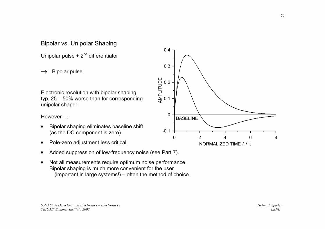
Bipolar vs. Unipolar Shaping
Unipolar pulse + 2nd differentiator
→ Bipolar pulse
Electronic resolution with bipolar shapingtyp. 25 – 50% worse than for correspondingunipolar shaper.
However …
• Bipolar shaping eliminates baseline shift(as the DC component is zero).
• Pole-zero adjustment less critical
• Added suppression of low-frequency noise (see Part 7).
• Not all measurements require optimum noise performance.Bipolar shaping is much more convenient for the user
(important in large systems!) – often the method of choice.
0 2 4 6 8NORMALIZED TIME t / τ
-0.1
0
0.1
0.2
0.3
0.4
AM
PLI
TUD
E
BASELINE