electronics laboratory- i experiments -...
TRANSCRIPT

1
BÜLENT ECEVİT UNIVERSITY
ELECTRICAL AND ELECTRONICS
ENGINEERING
ELECTRONICS LABORATORY- I
EXPERIMENTS
ORGANIZERS
Assist. Prof. Rukiye UZUN

2
BÜLENT ECEVİT UNIVERSITY
ELECTRICAL AND ELECTRONICAL ENGİNEERİNG
ELECTRONICS LABORATORY-I
EXPERIMENTS SHEET
ZONGULDAK, 2016

3
LABORATORY RULES
1) The laboratory is strictly forbidden to bring food and drinks
2) Laboratory during the course, make sure that your cell phones off or in
silent mode.
3) Students will come to class on time, otherwise; Students who are 10
minutes late are considered absent.
4) Speak in a low voice in order to ensure a productive work environment.
5) Each student coming lesson is responsible for all the experiments.
6) Students must bring the materials tested , otherwise; you are not allowed
in the experiment
7) Prohibited material exchange between the two groups.
8) During the experiment, the experiment can not be output without the
permission.
9) The materials used in the experiment such as measuring instruments,
cables, sources, test equipment should be used properly.
10) The instructor should be consulted about problems.
11) material left on the table, a group of students responsible for incomplete
or missing.
12) The instructor will be signed in the experiment measurements. Certainly
Students shall not be started other experiment without showing the results of
the experiment.
13) Reports shall be collected the following week course. Each student who
doesn’t bring to report for whatever reason will be zero.
14) At the end of the experiment the test panel cut all electrical devices,
electrical connection, the cables should be left disassembled parts, stools and
tables should be left tidy and clean way. Otherwise, the test results shall not
be signed.
15) All or part of another group Report All or a portion of the report can not
be same. Otherwise, copies of both reports and staple counted and the
experiment failed, even though they be considered to have been successful
in.
16) Due to valid reason, Students who miss more than two tests compensate
for missing experiments at the end of the term. (compensating week)
17) Students who miss more than two test will fail.
18) That not be in experiment the student's grade will be zero.

4
İçindekiler LABORATORY RULES ................................................................................................................................ 3
EXPERİMENT 1 ......................................................................................................................................... 6
DİODE CHARACTERİSTİCS ........................................................................................................................ 6
OBJECTİVE ............................................................................................................................................ 6
BILL OF MATERIALS ............................................................................................................................. 6
DESCRIPTION ....................................................................................................................................... 6
QUESTİONS .......................................................................................................................................... 8
EXPERİMENT 2 ......................................................................................................................................... 9
RECTİFİER CURCUİT ................................................................................................................................. 9
OBJECTİVE ............................................................................................................................................ 9
BILL OF MATERIALS ............................................................................................................................. 9
DESCRIPTION ....................................................................................................................................... 9
QUESTİONS ........................................................................................................................................ 11
EXPERİMENT 3 ....................................................................................................................................... 12
CLIPPING and CLAMPING CIRCUITS ....................................................................................................... 12
OBJECTİVE .......................................................................................................................................... 12
BILL OF MATERIALS ........................................................................................................................... 12
DESCRIPTION ..................................................................................................................................... 12
Clipping Circuit............................................................................................................................... 12
Clamping Circuits ........................................................................................................................... 14
EXPERIMENT 4 ....................................................................................................................................... 18
TRANSISTOR CHARACTERISTICS ............................................................................................................ 18
OBJECTIVE .......................................................................................................................................... 18
BILL OF MATERIALS ........................................................................................................................... 18
DESCRİPTİON ..................................................................................................................................... 18
Structure of Transistor .................................................................................................................. 18
Input Characteristic of Transistors ................................................................................................ 19
Output Characteristic of Transistors ............................................................................................. 20
EXPERIMENTAL WORK....................................................................................................................... 21
QUESTIONS ...................................................................................... Hata! Yer işareti tanımlanmamış.
EXPERİMENT 5 ....................................................................................................................................... 24
DC BİASİNG OF BJT TRANSİSTOR ........................................................................................................... 24
OBJECTİVE .......................................................................................................................................... 24

5
BİLL OF MATERİALS ........................................................................................................................... 24
DESCRİPTİON ..................................................................................................................................... 24
Transistor DC Polarization Circuits Most Commonly Used ......................................................... 25
1- Constant Beyz Polarization ........................................................................................................ 25
2- Stable Emitter Polarization Circuits ........................................................................................... 25
3- Voltage Divider Polarization Circuits ......................................................................................... 25
4- Collector Feedback Polarization Circuits ................................................................................... 26
EXPERIMENT 6 ....................................................................................................................................... 30
AC ANALYSIS OF AMPLIFIER CIRCUIT WITH TRANSISTOR ..................................................................... 30
OBJECTIVE .......................................................................................................................................... 30
BILL OF MATERIALS ........................................................................................................................... 30
THİNGS TO DO IN THE EXPERIMENT ............................................... Hata! Yer işareti tanımlanmamış.
EXPERIMENT 7 ....................................................................................................................................... 34
OBTAINING CHARACTERISTIC CURVES OF JFET ..................................................................................... 34
OBJECTIVE .......................................................................................................................................... 34
BILL OF MATERIALS ........................................................................................................................... 34
DESCRIPTION ..................................................................................................................................... 34
THINGS TO DO IN THE EXPERIMENT ............................................... Hata! Yer işareti tanımlanmamış.
EXPERIMENT 8 ....................................................................................................................................... 37
AMPLIFIERS OF JFET .............................................................................................................................. 37
OBJECTIVE .......................................................................................................................................... 37
BILL OF MATERIALS ........................................................................................................................... 37
DESCRIPTION ..................................................................................................................................... 37
THİNGS TO DO İN THE EXPERİMENT ............................................... Hata! Yer işareti tanımlanmamış.
APPENDİX ........................................................................................................................................... 40
1N4001 datasheet .............................................................................................................................. 40
2N2222 datasheet .............................................................................................................................. 41
2N2222A datasheet ........................................................................................................................... 42
BF245 datasheet ................................................................................................................................ 43
2N 3823datasheet .............................................................................................................................. 44
Preliminary Study, General Information about the Experiment and Report and Formats ................... 45
Cover Format ......................................................................................................................................... 46
Assessment ............................................................................................................................................ 47

6
EXPERİMENT 1
DİODE CHARACTERİSTİCS
OBJECTİVE
Examination of the diode characteristics
BILL OF MATERIALS
Diode: 2 units 1N4001 Silicon diode or the equivalent of it
Resistor: 2 units 1kΩ ve 470kΩ resistors
DESCRIPTION
Diode which is a semiconductor material passes current one diection better than other
direction The potential difference between the diode terminals determines whether or not we
diode conduction. If the anode is positive compared to the cathode, diode will forward current
and in this case the diode means that it is correct polarization. If it is positive compared to the
cathode to the anode, diode will allow you to pass through a very small leakage current and in
this case the diode means that it is reverse polarization.
In correct polarization, The voltage on the silicon diode is about 0.7V. (The voltage on
the germanium diode is about 0.3V.) Bu values are lower than the threshold voltage, diode
only allows a little current . This threshold voltage on the diode characteristic curve is called
twist. Because in this area, current through the diode voltage and falling on the diode voltage
range
Current voltage relationship is shown in figure 1:
Figıre1: I-V characteristic of a diode (Si Diode)

7
EXPERIMENTAL WORK
1) İn the figure 2 of the circuit, İf E = 5V and assuming the voltage drop across diode is
0.7V, Find the current through resistor in case of R =1kΩ. How does the diode polarize in this
circuit ? (Correct, Reverse)
2) İn the figure 3 of the circuit, İf E = 25V and assuming the voltage drop across diode is
0.7V , Find the current through resistor in case of R =470kΩ . How does the diode polarize in
this circuit ? (Correct, Reverse)
3) Execute the circuit in the Figure 2. E-voltage source sets for Vd values in Chart 1.
Register required measurement information in the table.
Chart 1
4) Using the values from obtaninig Chart 1 that the current and Vd , Plot the
characteristic curve of the diode I-V. (Using graph paper).
Vd (Volt) E (Volt) Vr (Volt) I=Vr/R
0
0.2
0.4
0.5
0.55
0.6
0.62
0.65
0.7
Figure-2 Figure 3

8
5) Execute the circuit in the Figure 3. E-voltage source sets for Vd values in Chart 2 .
Register required measurement information in the table. (For R=470kΩ).
Vd (Volt) E (Volt) Vr (Volt) I=Vr/R
0
-5
-10
-15
-20
-25
Chart 2
QUESTIONS 1. Explain What is the leakage current of the diode?
2. If a diode under forward polarization suddenly becomes reverse polarization, Explain
what could effect that blocks the passage cutting be?
3. If we did experiments using different diode , Would it be the difference characteristic
curves?

9
EXPERIMENT 2
RECTIFIER CURCUIT
OBJECTIVE
Learning how to work half and full-wave rectifier and reducing fluctuations (ripple) in the
output
BILL OF MATERIALS
Diode: 6 units 1N4001 Silicon diode or the equivalent of it
Resistors: 2 units 10kΩ, 2 units 470Ω
Potentiometer: 2 units 10kΩ
Capacitors: 1 units 220μF and 1 units 0.1 μF
DESCRIPTION
Half-wave and full-wave rectifications transform alternating current (AC) to direct current
(DC). This operation both may be possible with a single diode and may particularly connect
by linking diodes. A simple half-wave rectifier and a full-wave rectifier circuit are shown in
Figure 1 and Figure 2.
Figure 1 Half-wave rectifier

10
Figure-2 Full-wave rectifier
The important point of in the power sources is to minimize rectified output voltage ripple. To
minimize fluctuations, filtering process may be done. A simple filter circuit comprises a
capacitor connected in parallel rectifiers. The amplitude of the signal peak fluctuation
subjected to the filtering process:
ΔV =𝑉𝑚
𝑓𝑅𝐶
In this formula, R is load resistance, f is frequency value, C is the value of the capacitor and
Vm is the peak value of the input signal. The resulting DC signal amplitude:
𝑉𝑑𝑐 = 𝑉𝑚(1 −1
𝑓𝑅𝐶)
Ripple factor derived from the rectified signal is :
𝐷𝑎𝑙𝑔𝑎𝑙𝑎𝑛𝑚𝑎 % =1
2√3𝑓𝑅𝐶∗ %100
EXPERIMENTAL WORK
1. Execute the half-wave rectifier curcuit in the figure-3.(R=10kΩ, e(t)= 10Vt-t- 1kHz for
sinus wawe)
Figure 3

11
2. By getting the oscilloscope to DC, Measure e(t) peak value and VR(t) output value .
Plot wave graphics.
3. By reversing the diode terminals Figure-3, Repeat the process step 2.
4. Replace it with 5V square wave input signal e(t) in the Figure-3. Repeat the process
step 2.
5. Execute the curcuit in the figure-3 .(R= 10KΩ, e(t)=12V(peak to peak), f=1 kHz) And
By getting the oscilloscope to DC , Measure input voltage and voltage through the resistor.
Plot wave graphics.
Figure 4
6. Connect parallel 220µF capacitor to curcuit in the Figure 5. By getting the
oscilloscope to DC, Plot waveform through the 10KΩ resistor. (R= 10KΩ, e(t)=12V(peak to
peak), f=1 kHz).
Figure-5
7. Connect parallel the second 220µF capacitor to curcuit in the Figure 5. By getting the
oscilloscope to DC , Plot waveform through the 10KΩ resistor.
QUESTIONS 1. Explain what is the output capacitor function in the rectifier circuit?
2. Describe the relationship between the capacitance and the capacitor ripple factor.

12
EXPERIMENT 3
CLIPPING and CLAMPING CIRCUITS
OBJECTIVE
Understanding how to learn the working of principles of Clipping and clamping circuits
BILL OF MATERIALS
Diode: 2 units 1N4001 Silicon diode or the equivalent of it
Resistor: 2 units 10kΩ, 2 units 4.7KΩ, 1 unit 10MΩ, 1 unit 100Ω
Capacitor: 2 units 470μF
DESCRIPTION
Clipping Circuit
Any voltage level of input signal is above or below a certain part of the blinking circuit is
called clipping circuits. These circuits is used for rectifier curcuits, protection curcuits and a
wide variety of wave-shaping. A simple clipping circuit is shown at Figure-1.
Figure 1
Output signal is occured to clip small values of the input signal is zero volts and this is shown
at Figure-1. One of the clipper curcuits advantages can be replaced clipping level. İn other
words; the output voltage can be obtained from clipped desired signal voltage level.To
understand better at Figure 2. DC power source is connected to the diode in this circuit. To
pass the diode transmission in these circuits, the anode must have a more positive than
cathode (VDC < Vm olmalıdır). İn other words; when input signal exceeds VDC, diode can pass
transmission

13
Figure 2
When we analyze the circuit , DC source negative side is connected to the diode anode and
thus we can understand reverse polarity diode. To pass diode transmission, anode should be
more positive than cathode. İf this not happen, diode can’t pass transmission and output
voltage will always be zero.İf we analyze the positive alternans of input signal, when input
signal more greater than VDC, diode pass transmission and output become the difference
between value of the input voltage and VDC source . If we analyze peak value, this differance
become Vm-VDC (diode forward voltage threshold is ignored) and output peak value will be
Vm-VDC.
Parallel clipping occur that diode and output load or voltage connected in parallel. A simple
parallel clipping circuit is shown at Figure-3. At first, If the positive alternans active to circuit
input , diode cant pass transmission to be reverse polarization . (about open-circuit) And
Output voltage will be equal to input voltage. Secondly, when negatif alternans active to
circuit input, diode can pass transmission and diods will be zero volt . (refraction voltage is
neglected) Output voltage is equal to diode voltage or it is zero volt. Consequently ;This
circuit clips the negative alternans, but the input value is equal to the output without changing.
Figure-3
Clipping level can be brought desired level in the parallel clipping circuit like serial
circuit.For example; when we analyze the circuit at figure-4 , Clipping voltage is equal to -
VDC in the circuit output waveform and values are smaller than this values are clipped. Lets

14
look at the circuits to understand better . When the anode side of diode can be activeted –VDC
and input voltage is zero voltage, output voltage is zero.Also İf input voltage level is smaller
than –VDC level , cathode will be more negative than anode and diode vill be pass
transmission. In this case; output voltage is equal to –VDC ( refraction voltage is neglected).
When input voltage is smaller than -VDC , Output is always –VDC and Clipping process would
have occured.
Figure-4
Clamping Circuits
Clamping circuits is used for changing Dc voltage level applied to input. To do this, circuit
consisting of diode,capacitor and resistor should be used. Clamping circuits shift waveform
from negative area. This circuits are somitemes called level changer. Because they add
particular dc level to waveform. A simple clamping circuit is shown at Figure 5.
Figure 5
Circuit in the figure 6 clamps signal applied to input to zero DC level. For input signal
showing in the figure, on the diode will occur positive voltage in the period time between 0
and T/2. Diode acts as a short circuit in this case. Circuits is shown at Figure-a .

15
(a) (b)
Figure-6
Output of circuit is zero volt in this case and capacitor reachs peak voltage of input voltage (V
voltage ) in the short time. When input voltage is –V voltage (between T/2 and T) ,diode will
be negative voltage. Eventually circuit is as figıre-b. RC time constant should be great in this
circuit. Capacitor voltage must remain constant as far as possible in this time so RC should be
choosen great value. To remain constant between T/2 and T on the capacitor voltage, output
voltage is the sum of input and capacitor voltage. In other words, 𝑉𝑜 = 𝑉𝑖𝑛 − 𝑉𝑐 = −𝑉 − 𝑉 =
−2𝑉. Graph of the ınput and output voltage is shown at Figure-3.
Figure 3

16
EXPERIMENTAL WORK
Reminding: Waveform of input and output will be analayzed with the help of an
oscilloscope. Before you dont start the experiment, you must sure that oscilloscope calibration
adjustment is correct. Additionally, you sure that AC-GND-DC selector switch in the channel
entrances is DC position to see waveform. Because inputs is DC position, the importance of
the reference or zero point increases during the measurement. You perform the measurement
and ploting according to referance. Otherwise, your measurement and ploting will be wrong.
1. Execute the circuit shown below. (RL=10KΩ, VDC= 2V, Vİ input signal, f=1kHz,
10Vp-p sinüs ). First channel of oscilloscope will be input signal, second channel of it will be
output voltage . You sure that ground terminals of two channel and signal generator will be
connected ground terminal of circuit . Plot the input and output voltage that you see on the
two channel .After this, you will invert VDC source without changing value. Repeat the same
operations .
2. By inverting diode , Repeat seting up circuit executing in step 1. Register the
waveform of the input and output . After this, plot the input and output voltage by inverting
VDC source.
3. Set up parallel clipping as shown blow. (R = 4K7, VDC = 2V, Vİ =signal genator,
Vİ=10Vp-p, f=1kHz sinüs ). First channel of oscilloscope will be input signal, second channel
of it will be output voltage and register waveforms .Register input and output signal to figure
below by inverting diode.

17
4. Register input and output signal to figure below by inverting VDC source in the step 3.
After this, register waveform of input and output by inverting diode.
5. Set up clamping curcuit shown as blow.( RL=10K, C=470μF and Vİ is input signal,
from signal generator 1kHz, 10Vp-p square wave). First channel of oscilloscope will be input
signal, second channel of it will be output voltage Plot the input and output voltage that you
see on the two channel.
6. Set up the circuit shown as blow. Plot and register waveform of the input and output .(
VDC =2 V).Repeat the same operations by inverting DC source.

18
EXPERIMENT 4
TRANSISTOR CHARACTERISTICS
OBJECTIVE
Understanding the structure of transistors and determine the input and output characteristics
of transistors.
BILL OF MATERIALS
Transistor: 2 units 2N 2222 silisyum transistor or equavelant of it.
Resistors: 2 units 1kΩ, 2 units 100Ω
Potentiometer: 3 units 2 MΩ, 3 units 10 KΩ
DESCRIPTION
Structure of Transistor
BJT transistors are produced using doped P and N type materials. There are mainly two types
of NPN and PNP. NPN transistors include 2 units N type semiconductor materials and 1 unit
P type semiconductor material which is between of N type materials. PNP transistors include
2 units P type semiconductor materials and 1 unit N type semiconductor material which is
between of P type materials. Therefore, the transistor has 3 layers or terminals (Figure 1).
Figure 1: The physical structure and schematic symbols of NPN and PNP type transistors

19
In figure 2, it is given required polarity connections for NPN and PNP type transistors. It is
applied correct polarization towards base-emitter joint of the transistor by VBB source. It is
applied cross polarization towards base-collector joint of the transistor by VCC source.
Figure 2: The polarization of NPN and PNP transistors
Input Characteristic of Transistors
The characteristic curve shows the relationship of any current-voltage electrical materials.
Transistor has 2 different characteristic curves for input and output. Input characteristic of
transistor gives the relation between emitter voltage (VBE) and base current (IB) . To obtain the
input characteristic of transistor, collector-emitter voltage (VCE) is taken as a parameter and
base current (IB) is changed due to this voltage. It is measured the effect base emitter voltage
(VBE) because of changes of base current.
Figure 3: Input characteristic of the transistor.

20
As it can be seen from the graph, input characteristic of the transistor are similar to a normal
diode characteristic. While VBE voltage is less than 0.5 V, base current is so small that can be
negligible. Unless it is said in the applications, it can be accepted base-emitter voltage is equal
to 0.7 V when transistor start the transmission. Temperature can affect base emitter voltage
(VBE) a little part. For example, when the temperature increase each 1 degrees, VBE will
decrease about 2.3 mV.
Output Characteristic of Transistors
Output from the transistors is usually taken between collector-emitter poles. Therefore, output
characteristic of transistor gives changes of collector current (IC) and collector-emitter voltage
(VCE) which depends change of base current (IB) . VCE source which is applied to transistor is
important. This voltage should be equal to determined limit values. If the voltage exceed the
determined limit value, it causes deterioration due to occured refraction on the transistor.
Figure 4: Characteristics and refraction voltage of IC and VCE

21
EXPERIMENTAL WORK
1. Construct the following circuit to determine the characteristic of the common emitter
BJT circuit.
Figure 5
2. Obtain VCE and VBE for adjusting potantiometer to 1 MΩ and 10 KΩ by using values
at the Table 1. Measure and save values of VRB for each VCE and VBE values at the
Table1. It is advised using 2 measurement devices to be sure VCE value is constant.
VCE=3V VCE=5V
VBE VRB IB=VRB/RB VBE VRB IB=VRB/RB
0.60 0.60
0.62 0.62
0.65 0.65
0.67 0.67
Table 1
3. Investigate the output characteristic of following circuit which has a common emitter
adjust the value of potantiometer set to max value (10 kΩ). VCE will decrease about 0 V
because of this situation. After, adjust the potantiometer (1 MΩ) for IB will be equal to 10 μA

22
(It is important that when VRB is equal to 10 mV, IB is equal to 10 μA). After that, for each
values of VCE at the Table 2, adjust the potantiometer (10 kΩ) ensure IB will have constant
value.
Figure 6
4. Measure and save VRC by using each combination of VCE and IB values at the Table 2.
Table 2
5. Compute and save IB values at the Table 1. Draw input characteristic of the biasing
circuit by using these values which is given at the Table 1 and you have had before.

23
6. Compute and save IC values at the Table 2. Draw output characteristic which has
common emitter by using these values which is given at the Table 2 and you have
had before.

24
EXPERIMENT 5
DC BIASING OF BJT TRANSISTOR
OBJECTIVE
Anaylze DC biasing of BJT transistor connected to the common emitter and beyz.
BILL OF MATERIALS
Transistor: 2x2N2222A silicon transistor or equivalent
Direnç: 100Ω, 220Ω, 270Ω, 560Ω, 680Ω, 1KΩ, 1.2 KΩ, 2.2 KΩ , 3.3KΩ, 4.7KΩ, 5.6KΩ,
10KΩ, 33KΩ, 47KΩ, 100KΩ, 220KΩ, 270KΩ, 330KΩ, 470KΩ, 560KΩ, 1MΩ
Potentiometer: 2 units 10KΩ
DESCRIPTION
DC Polarization and Work Point
To use the transistor as amplifier or to amplify output voltage ( AC signal from the input ) , A
suitable DC polarization circuit is needed. If you are not a suitable DC polarization circuit,
transistor can not be used as an amplifier . So what does this mean DC polarization? Briefly,
it be defined as the providing of Proper working point or biasing of DC voltages between the
terminals of the transistor.
DC polarization circuit provides flowing static current from beyz,collector and emitter of
transistor. This meant that If there is an AC signal in the transistor inputs, ,Voltage and
current in the transistor will remain as static current and voltage. This situation is valid for
ideal conditions.Q working point is working point described above and symbols are added to
the subscript (Q) to determine current and voltage in this point. For example; IBQ and VCEQ
values respectively is voltage value of the transistor having beyz current and between
collector and emitter in the static working point.
Tempeture changings cause some negative effects on the transistor. Changing with
proportionately temperature and β being transistor current gain is the most importaant of
them. In other words; if the temperature increases, β increases so static working current and
voltage requested to remain stable will change . Different polarization circuits is used to
25
prevent the undesirede situation . We will analyze polarization circuits the most commonly
used and so understand transistor as usng amplifier .
Transistor DC Polarization Circuits Most Commonly Used
1- Constant Beyz Polarization,
2- Stable Emitter Polarization Circuits,
3- Voltage Divider Polarization Circuits,
4- Collector Feedback Polarization Circuits.
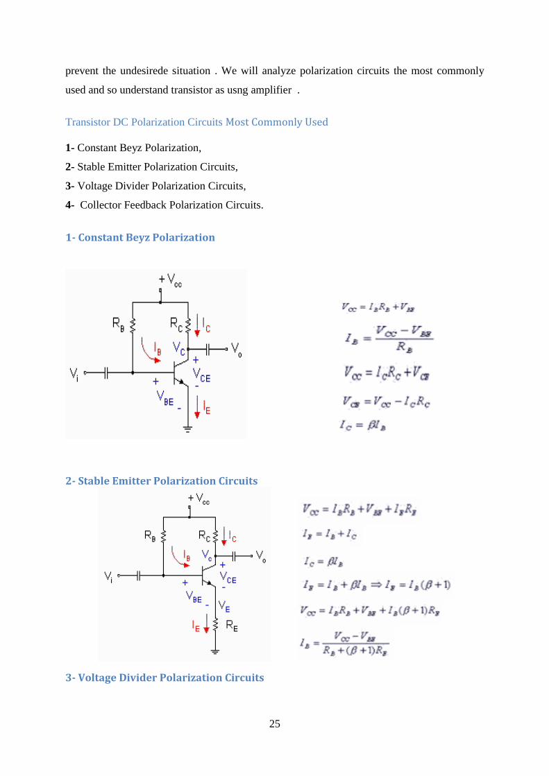
1- Constant Beyz Polarization
2- Stable Emitter Polarization Circuits
3- Voltage Divider Polarization Circuits

26
4- Collector Feedback Polarization Circuits

27
EXPERIMENTAL WORK
1. Anaylzing Common emitter connection ;
a) Set up the circuits as shown below.Measure the requirements for RB resistor given in
the table. (RC=270Ω, VCC=6V)
RB IB IC VRC VCE
100KΩ
330KΩ
560KΩ
1MΩ
b) Perfom the measurements required for any given value of RC to search effect of RC
resistor in the same circuits. (RB=330KΩ, VCC=6V)
RC IB IC VRC VCE
100Ω
270Ω
680Ω
1KΩ
2. Analyze Double Sourced Beyz joint connection;
a) Set up the circuit shown as blow. Perform the measurements required in table
(RC=2.2K, VCC=12V).

28
Figure-2 Double Sourced Beyz joint connection
b) Perfom the measurements required for any given value of RC in the same circuits
(RE=2.2K, VCC=12V, VEE= -2.8V)
RC IE VCB
5.6KΩ
3.3KΩ
1KΩ
560Ω
3. Analyze Single-Source Joint Beyz Connection;
Set up the circuit shown as blow. Measure IE current and VCT voltage for any given value of
RE, RC and RB in the table .(VCC=12V. VCT voltage is collector voltage.)
VEE RE IE VCB VCE
-2.8 560Ω
-2.8 1K Ω
-2.8 2.2K Ω
-1.4 560 Ω
-1.4 1K Ω
-1.4 2.2K Ω

29
Figure 3 Single-Source Joint Beyz Connection
RE RC RB IE VCT
10KΩ 10KΩ 100KΩ
10KΩ 10KΩ 47KΩ
10KΩ 10KΩ 33KΩ
5.6KΩ 10KΩ 100KΩ
5.6KΩ 10KΩ 47KΩ
5.6KΩ 10KΩ 33KΩ
10KΩ 5.6KΩ 100KΩ
10KΩ 3.3KΩ 100KΩ
10KΩ 1KΩ 100KΩ

30
EXPERIMENT 6
AC ANALYSIS OF AMPLIFIER CIRCUIT WITH TRANSISTOR
OBJECTIVE
Examine to the effects of amplifier characteristics the emitter resistance is completely
disabled, partially disabled and completely in-circuit.
BILL OF MATERIALS
Resistors: 2 x100Ω,1KΩ, 2.2KΩ, 10KΩ, 33KΩ
Capacitor: 2x4.7μF, 2x10μF, 2x47μF
Transistor: 2x2N2222A silisyum transistor or its compelent
EXPERIMENTAL WORK
1. Examine the emitter resistance is completely disabled.
Set the following circuit. Apply input of circuit sinusoidal signal with frequency 1KHz. Then
apply amplitutes values in Table 1. Observe the output signal with the aid of an oscilloscope.
Write Output voltage and current value on Table 1.
(RB1=33KΩ, RB2=10KΩ, RE1=100Ω, RE2=1KΩ, RC=2.2KΩ, transistor 2N2222A,
CB=10μF, CC=4.7μF, CE=47μF, VCC=12V )
Figure 1. Common emitter transistor circuit

31
Vin
(mV)
Vout
(mV)
AV
IB
(DC)
IC
(DC)
5
10
20
30
50
70
100
Table 1. Measuring Values
NOTE: without breaking the circuit, find IB current for Vin=40mV.
2. Examine the emitter resistance is partially disabled.
Set the following circuit. Apply input of circuit sinusoidal signal with frequency 1KHz. Then
apply amplitutes values in Table 2. Observe the output signal with the aid of an oscilloscope.
Write Output voltage and current value on Table 2.
(RB1=33KΩ, RB2=10KΩ, RE1=100Ω, RE2=1KΩ, RC=2.2KΩ, transistör 2N2222A,
CB=10μF, CC=4.7μF, CE=47μF, VCC=12V)

32
Figure 2. Common emitter transistor circuit
Vin
(mV)
Vout
(mV) AV
5
10
20
30
50
70
100
200
Table 2. Measuring Values
NOTE: without breaking the circuit, find IB current for Vin=40mV.
3. Examine the emitter resistance is completely in-circuit.
Set the following circuit. Apply input of circuit sinusoidal signal with frequency 1KHz. Then
apply amplitutes values in Table 3. Observe the output signal with the aid of an oscilloscope.
Write Output voltage and current value on Table 3.
(RB1=33KΩ, RB2=10KΩ, RE1=100Ω, RE2=1KΩ, RC=2.2KΩ, transistor 2N2222A,
CB=10μF, CC=4.7μF, CE=47μF, VCC=12V).

33
Figure 3. Emitter resistance is completely in-circuit
Vin
(mV)
Vout
(mV) AV
5
10
20
30
50
70
100
200
300
Table 3. Measuring Values
NOTE: Without breaking the circuit, find IB current for Vin=40mV.
4. Find input impedances corresponding IB for each circuit for Vin=40mV. Compare them
each other. Put in order the three circuits in terms of input impedance.

34
EXPERIMENT 7
OBTAINING CHARACTERISTIC CURVES OF JFET
OBJECTIVE
To obtain characteristic curves of JFET.
BILL OF MATERIALS
Transistor: 2x BF245 transistor or its compelent
Resistors: 2 x100Ω,2x1kΩ, 2x2.2KΩ,2x270KΩ
DESCRIPTION
FET is called unipolar (single pole) on the contrary BJT transistors. Because FET is only one
load carrier. When gate-source voltage (VGS) of N-channel JFET transistor is negative,
Current flow is made from drain to source. While VGS voltage is 0V, G-D junction is reverse
polarized and not current flows. On the contrary BJT transistors, output current ID is
controlled by VGS voltage. Output current IC is controlled by the input current IB in BJT.
Figure 1 seems to be the relationship between the output current ID input voltage VGS. ID
and VGS 's max values must be known in order to calculate the current and voltage in
operating point. If VGS = 0 V, ID current max value, and is called IDSS (Drain saturation
current). If VGS voltage is increased (negative will be increased) ID current will be equal to 0
at a point. When ID = 0 VGS voltage is called VP (pinch-off voltage).
Figure 1
35
At the time of the study point to calculate the current and voltage, the equations of figure.1 are
solved at the same time. On the left side of equations is transfer equation of the transistor. On
the right side of the equation is load line equation for JFET circuit
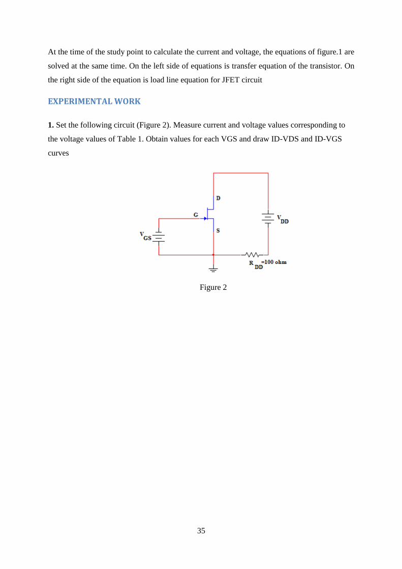
EXPERIMENTAL WORK
1. Set the following circuit (Figure 2). Measure current and voltage values corresponding to
the voltage values of Table 1. Obtain values for each VGS and draw ID-VDS and ID-VGS
curves
Figure 2

36
Table 1 Voltage value of applied to circuit
2. a) Set the following circuit (Figure 3). Measure ID current, VGS and VDS voltage.
Figure 3
b) Make RD resitance value is 1kΩ and repeat option of a
c) Make RD resitance value is 1kΩ, RS resitance value is 2.2kΩ and repeat option of a.
d) Make RD resitance value is 2.2kΩ, RS resitance value is 1kΩ and VD voltage value is 10V
and then repeat option of a.
VDD(V) VGS(V) ID(mA) VDS(V) VDD(V) VGS(V) ID(mA) VGS(V)
0 0 0 -1
1 0 1 -1
5 0 5 -1
10 0 10 -1
12 0 12 -1
0 -0.5 0 -2
1 -0.5 1 -2
5 -0.5 5 -2
10 -0.5 10 -2

37
EXPERIMENT 8
AMPLIFIERS OF JFET
OBJECTIVE
Learning AC analyses of amplifier with JFET.
BILL OF MATERIALS
Transistor: 2x 2N3823 JFET or its compelent.
Capacitor: 2 adet 33μF, 2 adet 10μF.
Resistors: 2 adet 1MΩ, 2 adet 2.2kΩ, 2 adet 1.1kΩ.
DESCRIPTION
FET's input resistance is much higher than bipolar transistor, so FETs are more preferred. On
semiconductor characteristic values: selection of ID, VDS, VGS values (determination of the
operating point), then initially calculated RD=(VDD-VDS+VGS)/ID value. The negative
voltage is provided by RSS between gate and emetor. Deliberately, R1=1MΩ is selected, and
İf any current never flows through gate, VR1= 0V. This means is that the gate voltage is at
ground potential. In this case, only ID current will flow on RSS. As a result, RSS=- VGS/ID
is obtained.
C1 capacitance is put into for coupling AC signals. capacitance is effective at low
frequencies. R1>1/wC1 condition must be satisfied for a good low-frequency response. This
inequality 10-fold difference R1=10/wC1 will be sufficient. R1=1.5MΩ and the lower cut-off
frequency selected for fa C1=10/(2π fa R1) .
Not to change the emitter voltage of AC signals, CSS bridging capacity are connected. CSS
impedance value must be much lower than from RSS by the value of signal frequency, so
terminal of the emitter is grounded. according to this CSS= 10//(2π fa RSS) is used.

38
EXPERIMENTAL WORK
1. Given above for the integration of the 2N3823, Calculate the operation point VDS-ID
graphical structure for ID=2mA VDS=6V ve VGS=-2V
2. Standard values are given in relation to the operating point. However, the full value of
the operating point is not given. Save the appropriate point in calculating these values.
Operating Point:
VDS= ____ VGS= ____ ID=____
RD(calculated)=____ RD(used)= 2.2kΩ
RSS(calculated)=____ RSS(used)= 1.1kΩ
Low cut-off frequency = 100Hz
C1 (calculated)=_____ C1(used)= 10μF
CSS(calculated)=____ CSS(used)= 33μF
3. Set the citcuits given above using on values. Circuit input is applied 10 mVpp, 30 mVpp
50 mVpp and 100 mVtt - 1 kHz frequency. Calculate the value of the output signal
using ossiloscope and calculate gain.
For Vi=10 mVpp, 30 mVpp 50 mVpp and 100 mVtt , V0=______ AV= V0/ Vi=__________

39
Increase the input signal until distortion the output signal. When distortion takes place ,Is
equal to the amplitude of the output signal of positive and negative half-cycles? What is the
reason for the difference?
Vi(starts distortion)=______ , V0(starts distortion)=_______

40
APPENDİX
1N4001 datasheet
7
41
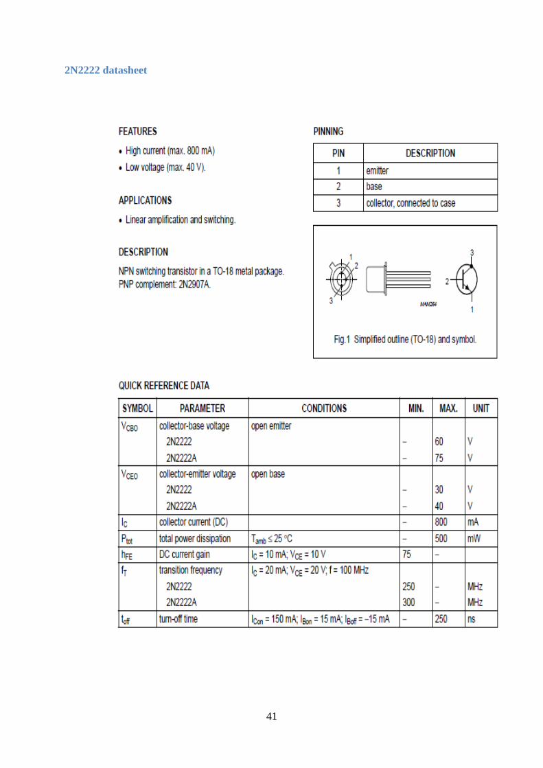
2N2222 datasheet

42
2N2222A datasheet

43
BF245 datasheet

44
2N 3823datasheet

45
Preliminary Study, General Information about the Experiment and Report and Formats
Preliminary Study: Her deney için, “DENEYDE YAPILACAKLAR (EXPERIMENT
WORK)” kısmı sırası ile en iyi bildiğiniz bir simülasyon programı ile simülasyonları
yapılacak ve A4 kağıda yapılan simülasyonların çıktıları alınıp Laboratuara gelinecektir.
Experiment: Ön çalışmalarını yapan bireyler deney esnasında elde ettikleri sonuçları A4
kağıdına grup numarası, ad soyad ve imzaları ile birlikte görevli Hocalarımıza teslim
edeceklerdir. Bir kopyasını kendinize almayı unutmayınız.
Report: Rapor tamamen deney esnasında elde ettiğiniz sonuçların yorumları ile birlikte bir
sonraki hafta deneye gelirken teslim edilmesidir. Grup olarak hazırlanacaktır. Rapor formatı
aşağıdadır:
Devrenin Çizimi
Devrenin simülasyon
çıktısı (grafik yada
tablo)
Deneyde elde edilen
sonuçları (grafik yada
tablo)
Elde edilen sonuçların yorumlanması

46
Cover Format
BÜLENT ECEVİT UNIVERSITY
ELECTRICAL AND ELECTRONICAL ENGINEERING
2016-2017
ELECTRONICS LABORATORY-I
REPORT
EXPERIMENT NO: 3
EXPERIMENT NAME: CLIPPING AND CLAMPING CURCUITS
GROUP NO: 5
GROUP MEMBERS:
Osman DALBUDAKOĞLU Signature
Ozan GÜLBUDAKOĞLU Signature

47
Assessment
*Vize ve Final sınavları yazılı olacaktır.(Vize ve final haftalarında)
** Project
1- 21 kasım 2016 tarihine kadar proje ara raporunu teslim edilecek.
2- 12 aralık 2016 tarihine kadar projelerin bitmiş ve çalışır halleri teslim edilecek. Proje
ile ilgili sözlü sınava tabi tutulacaksınız.
Not: Tarihlerde değişiklik yapılabilir.
GENEL
NOT
(%100)
YIL İÇİ
(%50)
YIL
SONU
(%50)
RAPOR
(%25)
FİNAL*
(%20)
PROJE**
(%30)
VİZE*
(%25)