electrostatic discharge and electromagnetic … electrostatic discharge and electromagnetic...
TRANSCRIPT

1
Electrostatic Discharge and Electromagnetic Interference Design
and Testing of Power Plant Safety Control Cabinet
A Major Qualifying Project Report Submitted to the Faculty
of the
WORCESTER POLYTECHNIC INSTITUTE
in partial fulfillment of the requirements for the Degree of Bachelor of Science
in Electrical and Computer Engineering by
___________________________________ Jola Myrta
Approved by:
____________________________________ Professor Peder C. Pedersen
March 1, 2010

2
Table of Contents
Table of Contents ........................................................................................................................ 2 Table of Figures .......................................................................................................................... 4 Table of Tables ........................................................................................................................... 6 List of Equations ......................................................................................................................... 7 Acknowledgements ..................................................................................................................... 8 Abstract ....................................................................................................................................... 9 1. Introduction ........................................................................................................................... 10 2. Background ........................................................................................................................... 12 2.1 Nuclear Industry.................................................................................................................. 12 2.2 Standards ............................................................................................................................. 12 2.3 Pressure Water Reactor ....................................................................................................... 13 2.4 Shin Kori 3 & 4 APR1400 .................................................................................................. 15 3. Auxiliary Process Cabinet- Safety ........................................................................................ 17 3.1 Qualification Requirements ................................................................................................ 17 3.2 Equipment Safety Classification ......................................................................................... 18 3.3 Acceptance .......................................................................................................................... 19 3.3.1 Seismic ............................................................................................................................. 19 3.3.2 Environmental .................................................................................................................. 19 3.4.3 Electromagnetic Compatibility ........................................................................................ 19 3.4.4 Fault ................................................................................................................................. 20 4. Test Procedure for Monitoring the Signal Conditioning ...................................................... 21 4.1 Modules............................................................................................................................... 21 5. Electrostatic Discharge ......................................................................................................... 24 5.1 Introduction ......................................................................................................................... 24 5.1.1 Human Body Model ......................................................................................................... 25 5.1.2 Machine Model ................................................................................................................ 26 5.1.3 Charged Device Model .................................................................................................... 27 5.2 Electrostatic Discharge of Signal Conditioning Modules ................................................... 28 5.3 Design of Enclosure ............................................................................................................ 28 5.3.1 Software Used .................................................................................................................. 29 5.3.2 Machining ........................................................................................................................ 31 5.4 Software Analysis ............................................................................................................... 31 5.4.1 Background of Electromagnetism .................................................................................... 32 5.4.2 Testing and Analysis ........................................................................................................ 35 5.4.3 Results .............................................................................................................................. 36 6. Results ................................................................................................................................... 55 6.1 Introduction ......................................................................................................................... 55 6.2 ESD Test Results ................................................................................................................ 57 6.2.1 Modules............................................................................................................................ 57 6.2.2 Aluminum Enclosure ....................................................................................................... 58 6.2.3 Stainless Steel Enclosure ................................................................................................. 59 6.3 Compare Software and Testing Results .............................................................................. 59 7. Conclusions .......................................................................................................................... 60

3
References ......................................................................................................................... ……62 Appendix A: Standards ............................................................................................................. 63 Appendix B: Wiring Diagrams For Each Module ................................................................... 64 Wiring description for the W5206 ............................................................................................ 64 Wiring description for the W5207 ............................................................................................ 65 Wiring description for the W5214 ............................................................................................ 66
Wiring description for the W5229 ........................................................................................ 67 Wiring description for the W5216 ........................................................................................ 68 Wiring description for the W5218 ........................................................................................ 69 Wiring description for the W5221 ........................................................................................ 70 Wiring description for the W5224 ........................................................................................ 71 Wiring description for the W5227 ........................................................................................ 72 Wiring description for the W5228 ........................................................................................ 73 Wiring description for the W5204 ........................................................................................ 74 Wiring description for the W5202 ........................................................................................ 75 Wiring description for the W5205 ........................................................................................ 76
Appendix C: Test Equipment.................................................................................................... 77 Appendix D: Test Setup ............................................................................................................ 78 Appendix E: Expected Outputs with Tolerances ...................................................................... 80 Appendix F: Ideal Expected Outputs ........................................................................................ 82

4
Table of Figures Figure 1 Artist Rendition of Shin Kori 3&4 ................................................................................ 17 Figure 2: Wiring of the Modules inside cabinet ........................................................................... 22 Figure 3: Fluke Calibrators ........................................................................................................... 22 Figure 4: Output to the Datalogger ............................................................................................... 22 Figure 5: Wiring diagram from terminal blocks to input and output module ............................... 23 Figure 6: Typical Human Body Model Circuit ............................................................................. 25 Figure 7: Worst Case, Actual Human Body Model Circuit .......................................................... 26 Figure 9: Machine Model Circuit ................................................................................................. 26 Figure 10: Charged Device Model ................................................................................................ 27 Figure 11: Dimensions of Module Make ...................................................................................... 29 Figure 12: Sheet metal Design ...................................................................................................... 30 Figure 13: Top Sheet Metal Design .............................................................................................. 30 Figure 14: Enclosure with Module ............................................................................................... 31 Figure 15: Global Setup ................................................................................................................ 35 Figure 16: Aluminum Impressed x E-Field .................................................................................. 36 Figure 17: Arrows of electric field strength .................................................................................. 37 Figure 19: Values for chosen point on surface ............................................................................. 38 Figure 18: Chosen value on surface .............................................................................................. 38 Figure 20: Graph of front .............................................................................................................. 39 Figure 21: Aluminum Impressed y E-field ................................................................................... 39 Figure 22: Arrows of electric field strength .................................................................................. 40 Figure 24: Values from chosen point on surface .......................................................................... 41 Figure 23: Chosen value on surface .............................................................................................. 41 Figure 25: Graph of Front ............................................................................................................. 42 Figure 26: Aluminum Impressed z E-field ................................................................................... 42 Figure 27: Arrows of electric field strength .................................................................................. 43 Figure 28: Chosen value on surface .............................................................................................. 44 Figure 29: Values from chosen point on surface .......................................................................... 44 Figure 30: Graph of front .............................................................................................................. 45 Figure 31: Stainless Impressed x E-field ...................................................................................... 45 Figure 33: Chosen value on surface .............................................................................................. 46 Figure 32: Arrows of electric field strength .................................................................................. 46 Figure 34: Values from chosen point on surface .......................................................................... 47 Figure 35: Graph of front .............................................................................................................. 47 Figure 36: Stainless Impressed y E-field ...................................................................................... 48 Figure 37: Arrows of electric field strength .................................................................................. 48 Figure 39: Values from chosen point on surface .......................................................................... 49 Figure 38: Chosen value on surface .............................................................................................. 49 Figure 40: Graph of front .............................................................................................................. 50 Figure 41: Arrows of electric field strength .................................................................................. 51 Figure 43: Values from chosen point on surface .......................................................................... 52 Figure 42: Chosen value on surface .............................................................................................. 52 Figure 44: Graph of front .............................................................................................................. 53 Figure 46: Set-up of test bench ..................................................................................................... 56

5
Figure 45: Test Levels .................................................................................................................. 56 Figure 47: Data Logger Software ................................................................................................. 57 Figure 48 Wiring diagram for the W5206 .................................................................................... 64 Figure 49 Wiring diagram for the W5207 .................................................................................... 65 Figure 50 Wiring diagram for the W5207 .................................................................................... 66 Figure 51 Wiring diagram for the W5229 .................................................................................... 67 Figure 52 Wiring diagram for the W5216 .................................................................................... 68 Figure 53 Wiring diagram for the W5218 .................................................................................... 69 Figure 54 Wiring diagram for the W5221 .................................................................................... 70 Figure 55 Wiring diagram for the W5224 .................................................................................... 71 Figure 56 Wiring diagram for the W5227 .................................................................................... 72 Figure 57 Wiring diagram for the W5228 .................................................................................... 73 Figure 58 Wiring diagram for the W5204 .................................................................................... 74 Figure 59 Wiring diagram for the W5202 .................................................................................... 75 Figure 60 Wiring diagram for theW5205 ..................................................................................... 76

6
Table of Tables Table 1: Electric Field Strength of Aluminum and Stainless Steel .................................. 53 Table 2: Results for Aluminum......................................................................................... 58 Table 3: Results for Stainless Steel ................................................................................... 59

7
List of Equations Equation 1: Output Calculation for the W5206 Module ................................................... 82 Equation 2: Output Calculation for the W5207 Module ................................................... 82 Equation 3: Output Calculation for the W5214 Module ................................................... 83 Equation 4: Output Calculation for the W5229 Module ................................................... 83 Equation 5: Output Calculation for the W5216 Module ................................................... 84 Equation 6: Output Calculation for the W5218 Module ................................................... 84 Equation 7: Output Calculation for the W5221 Module ................................................... 85 Equation 8: Output Calculation for the W5224 Module ................................................... 85 Equation 9: Output Calculation for the W5227 Module ................................................... 86 Equation 10: Output Calculation for the W5228 Module ................................................. 86 Equation 11: Output Calculation for the W5204 Module ................................................. 87 Equation 12: Output Calculation for the W5202 Module ................................................. 87 Equation 13: Output Calculation for the W5205 Module ................................................. 88

8
Acknowledgements I would like to thank Professor Peder Pedersen for advising this project. I would like to
acknowledge Westinghouse Electric Company, for their funding and opportunity to allow WPI
to be a part of their cutting edge research and development. I also offer gratitude to
Westinghouse Nuclear Company for the travel and testing experience conducted in New Stanton,
PA. I would like to acknowledge Integrated Software for their COULOMB3D electric field
solver software.

9
Abstract
This project conducts an innovative approach to prevent electromagnetic interference and
electrostatic discharge affecting the Auxiliary Process Safety Cabinet (APC-S) in the South
Korean Nuclear Power Plant 3 and 4, also known as Shin Kori 3 &4. The Auxiliary Process
Safety Cabinet consists of the Acromag Signal Conditioners and is required to function and
maintain structural integrity before, during and after all tests. Research was conducted on the
causes and how to prevent electrostatic discharge from damaging electric components. As the
signal conditioners were provided from a manufacturer the design of the components could not
be changed. The solution was to design a metal enclosure to protect the inside components from
any electrostatic discharge. The modules needed to be accessible in the enclosure in case of any
failure. This then lead to the idea of having an enclosure that consisted of two parts. By
designing a metal enclosure for the Acromag signal conditioner modules it was proven that they
passed Electrostatic Discharge testing. This was shown by conducting both software analysis and
testing on aluminum and stainless steel enclosures.

10
1. Introduction
This project conducts an innovative approach to prevent electromagnetic interference and
electrostatic discharge affecting the Auxiliary Process Safety Cabinet (APC-S) in the South
Korean Nuclear Power Plant 3 and 4, also known as Shin Kori 3 &4. The APC-S cabinet will be
tested for Seismic, Electromagnetic, Environmental and Electrostatic Discharge. This project
will focus on the design and testing for electrostatic discharge. The cabinet is required to
function and maintain structural integrity before, during and after all tests.
This project will consist of the design of the Auxiliary Process Cabinet- Safety and an enclosure
design of the Acromag modules to be protected from Electrostatic discharge. The design of the
APC-S consists of 13 Acromag signal conditioner modules that receive signals from different
sensors throughout the plant and split the signals to a safety and non-safety system. It is
important for these modules to maintain their functionality so that these two systems do not
communicate with one another.
Engineering activities in this project has included the design of the final wiring diagram, the
drawings of the test set up as it is placed in the cabinet, and the set up of all modules and mount
into cabinet connect both the input and output. The final wiring diagram was determined after the
functions of the 13 modules were studied. In the drawing the input of the module is shown and
the output that is connected to the data logger. The design of an aluminum and stainless steel
enclosures was important to protect the modules from high voltages, electrostatic discharge. The
modules were only tested at medium level. Numerical software that will predict the field
distribution for the enclosure in orthogonal directions was conducted using COULOMB software.

11
The software was important to predict if the modules would pass. The modules were then
manufactured after being designed in SolidWorks at the machine shop at Worcester Polytechnic
Institute. After the modules enclosures were completed they were sent down to complete
experimental testing that was conducted in New Stanton, PA by Washington Labs Facility. The
data collected from testing of the modules was then compared to the experimental results of
COULOMB.
The output data was recorded using the FLUKE 2640/2645 NetDAQ Data Logger. This data
logger will read all of the output results every 1/10 seconds. The software that was used to run
analytical field distributions is Integrated Software COULOMB.7. COULOMB.7 provides many
features such as analysis of electrical conduction and loss dielectrics, simulation of non-linear
conductivity and permittivity, and ability to assign constant or non-uniform charge distributions
to surfaces, as well as many other features.
In the second chapter background of the nuclear industry and the design of this nuclear power
plant, Shin Kori 3 & 4 is presented. In the third chapter the Auxiliary Process Cabinet is
introduced and the tests that are being conducted. In the fourth chapter the modules and their
functions are explained. In the fifth chapter electrostatic discharge research is shown and the how
it will affect the modules. Lastly in chapter six the results for software analysis and experimental
testing are compared.

12
2. Background
2.1 Nuclear Industry
The nuclear industry began with the Manhattan Project of World War II, which ended in the
making of the first atomic bombs. After the war ways were sought to bring peaceful and
commercial uses to this new technology. In the early 1950s, a bill was signed into creating the
Atomic Energy Commission with the purpose to promote and control the use of the atom. As
technology grew the laws and regulations changed to reflect the knowledge learned and establish
limits for construction and operation.
In 1954 the Nuclear Regulatory Commission was formed to oversee, set rules and standards for
the commercial use of nuclear materials. The Atomic Energy Commission were not only
regulating the industry but also promoting it. In the 1970s the commission stopped promoting
nuclear power but continues to regulate the industry due to Three Mile Island. The Nuclear
Regulatory Commission consists of five commissioners one of which is named Chairman by the
United States of America. The NRC protects the health and safety of the general public.
2.2 Standards
Agencies in charge of providing guidelines of the nuclear power industry are American National
Standards Institute (ANSI), American Society of Mechanical Engineers (ASME), Institute of
Nuclear Power Operations (INPO), International Commission on Radiological Protection (ICRP),
International Commission on Radiation Units (ICRU), National Council on Radiation Protection
and Measurement (NCRP), Institute of Electrical and Electronics Engineers (IEEE) and more.

13
The ASME provides guidelines and standards on piping, valves and mechanical systems. INPO
was formed to provide an independent group which sets standards of excellence. ICRP and
ICRU have set radiation standards on international level while NCRP has done the same thing in
the United States. The purpose of the agencies is to provide standards, limits, and guidelines
which protect the public and workers and still provide freedom for the economical incentive for
nuclear power.
2.3 Pressure Water Reactor
A pressurized water reactor system utilizes two separate heat transfer loops to accomplish the
production of steam for turbine-generator operation. These heat transfer loops are referred to as
the primary system and the secondary system. The primary loop consists of the reactor vessel,
reactor coolant pumps, pressurizer, steam generator tubes and interconnecting piping. The
secondary system consists of the shell side of the steam generators; high and low pressure
turbines, moisture/separator re-heaters, main electrical generator, main condenser, condensate
and feed pumps, and interconnecting piping.
Pressurized water reactor defines the coolant to be used as the heat transfer medium, and
describes the conditions at which the coolant will exist. The coolant used is light water which is
pressurized at approximately 2250psi. The coolant is pressurized so that its temperature can be
raised above the boiling point of 212°F allowing for the production of steam in the secondary
side of the steam generator.
In operation, the uranium fuel in the reactor vessel produces large amounts of heat during the
fission process. The reactant coolant flows past the fuel in the channels in the core and absorbs

14
the heat being produced. The coolant is then pumped through the tubes in the steam generator
where this excess heat is transferred to the feedwater surrounding these tubes. This heat transfer
causes the feedwater to boil, producing steam in the secondary side of the steam generator. A
large storage vessel is connected to the loop to absorb changes in the coolant volume and to
maintain system pressure at the required 2250psi. The reactant coolant system is maintained in a
sub cooled liquid state to prevent possible fuel or system damage. The temperature-pressure
relationship of the coolant should be maintained within a normal range to prevent bulk boiling.
In the secondary system, the steam produced by the boiling of feedwater is directed to high and
low pressure turbines which are coupled to an electrical generator. The steam is used to rotate the
high and low pressure turbines which causes condensed in the main condensers and this
condensate is pumped to the feed pump suction. The feed pump raises the pressure of the
feedwater and pumps it back into the steam generator to repeat the cycle.

15
2.4 Shin Kori 3 & 4 APR1400
This section explains on how the Shin Kori power plant will run and how much power it will
produce. Although this project is a small part of a power plant every single component needs to
be operating at the exact specification for it this plant to properly produce power. The APR1400
is an evolutionary advanced light water reactor based on the Westinghouse Combustion
Engineering (CE) System 80+ technology. The 80+ standard plant design is a 1300 MWe1
pressurized water reactor based on evolutionary improvements to the standard CE System 80
nuclear steam supply system and a balance-of-plant design developed by Duke Power Co. The
System 80+ design has safety systems that provide emergency core cooling, feedwater and decay
heat removal. It also contains a safety depressurization system for the reactor, a combustion
turbine as an alternate AC power source, and an in-containment refueling water storage tank to
enhance the safety and reliability of the reactor system.
The nuclear steam supply system of the APR1400 is rated at 4,000 MWt2
with a net electrical
generation of 1,400 MWe. The Korean Nuclear Industry decided to standardize its advanced
reactor design based on this technology in the mid-1990s and spent the next 10 years developing
the detailed design. Westinghouse participated in this design effort under the Korean Next
Generation Reactor (KNGR) contract executed from 1997 through 2000. This partnership
eventually translated into signing of the SKN 3&4 contract in September 2006.
The scope for the two units consists of component design, equipment supply, project
management, and consulting services. Major mechanical equipment supplied under the contract
1 Megawatt Electric which refers to electric power 2 Megawatt Thermal which refers to thermal power produced

16
consists of equipment manufactured at Nuclear Components Manufacturing, including one set of
reactor vessel internals; eight reactor coolant pumps; one set of control element drive
mechanisms and associated tooling; and control element assemblies, manufactured by
Westinghouse Nuclear Fuel. Also supplied were reactor coolant pump motors, reed switch
position indicators, the boronometer, and the process radiation monitor, all purchased from
outside vendors. In addition to the mechanical equipment, Westinghouse will supply an
integrated I&C architecture for both the Nuclear Steam Supply System (NSSS) I&C and the
balance-of-plant systems and control facilities, which is a major difference between Shin Kori 3
and 4 and previous Korean Standard Nuclear Plants. The NSSS I&C includes the protection
systems and NSSS-related control and monitoring. The balance-of- plant I&C includes systems
for safety and non-safety component control, man-machine interfaces, and the control-room
facilities.
Shin Kori 3&4 will be the thirteenth and the fourteenth nuclear units in the Republic of South
Korea based on Westinghouse CE technology, as well as the nineteenth and twentieth overall
based on Westinghouse technology. Shin Kori consists of 6 units total, 1&2, 3&4 and 5&6.
Currently, Shin Kori 1 &2 are under construction.

17
Figure 1 Artist Rendition of Shin Kori 3&4
3. Auxiliary Process Cabinet- Safety
The Auxiliary Process Cabinet for Safety and Non-Safety houses analog signal conditioning and
splitting electronics for the Reactor Coolant Pump Speed Sensors and conventional field
instrumentation. The signal conditioners and splitters receive signals from various field sensors
which condition and split, transmitting the output signal to different system such as the safety
and non safety, and cabinets throughout the Nuclear Power Plant.
3.1 Qualification Requirements
The purpose of qualification requirements is to identify the equipment qualification actions
required to be performed by the Signal Conditioning Instrumentation equipment supplier for the
Shin-Kori Units 3 and 4 nuclear power plants and that requirements are met. The signal
conditioning components are planned to be used in the Safety System Cabinets of the Auxiliary
Process Cabinet-Safety (APC-S), Core Protection Calculator System (CPCS), Qualification and
Indication Alarm System- PAMI (QIAS-P), and the Engineered Safety Feature- Component
Control System (ESF-CCS) Group Controllers and Loop Controllers.

18
This specification defines the seismic, environmental, Electromagnetic Compatibility (EMC),
and fault isolation test conditions, specific qualification requirements and methods to be
employed in the performance of the qualification activities. The equipment shall meet the
required performance requirements during seismic, environmental, EMC, and fault isolation
testing.
The Safety System Cabinets in which the signal conditioning equipment will be installed are
required to be qualified as Seismic Category I. The signal conditioning equipment is required to
function and maintain structural integrity during and after design basis event conditions.
3.2 Equipment Safety Classification
The highest classification of the safety-related signal conditioning equipment planned to be used
for SK3&4 is Class 1E, Seismic Category I. Class 1E (Safety) Seismic Category I equipment is
required to function and maintain structural integrity before, during and after a Safe Shutdown
Earthquake (SSE) seismic event. Non-safety related equipment whose continued function is not
required but whose failure could impact proper functioning of adjacent safety-related Seismic
Category I equipment is defined as
Non-Safety, Seismic Category II. Non-Safety, Seismic Category II equipment must maintain
structural integrity during and after the SSE. The signal conditioning equipment planned to be
used in SK3&4 will be used in both Class 1E (Safety) Seismic Category I and Non-Safety
Category II applications.

19
3.3 Acceptance
Qualification activities performed shall demonstrate the signal conditioning equipment meets the
seismic, environmental, EMC, and fault isolation requirements.
3.3.1 Seismic
Seismic qualification performed shall demonstrate that the Seismic Category I Signal
Conditioning Equipment will maintain structural integrity during and after an earthquake at the
SSE level preceded by the equivalent of five earthquake simulations at the one-half SSE level.
Signal Conditioning Equipment is required to demonstrate it can perform its designated safety
related functions before, during, and after each seismic test.
3.3.2 Environmental
Environmental qualification performed shall demonstrate the signal conditioning equipment
continues to perform its designated safety related functions when subjected to the temperature
and humidity conditions contained within this specification. Additionally, a qualified life for the
Class 1E signal conditioning equipment shall be determined in accordance with the requirements
of IEEE-323-1983 as noted by Regulatory Guide 1.89.
3.4.3 Electromagnetic Compatibility
Electromagnetic Compatibility testing shall be performed to demonstrate the signal conditioning
equipment continues to perform its designated safety-related functions during and after
continuous and transient EMC events. The signal conditioning equipment shall be designed to
lower the susceptibility to externally generated EMI/RFI and power surges. The Supplier shall

20
also design the system to minimize the generation of EMI/RFI, thus becoming a potential source
of interference as described in WNA-DS01220-SHIN-K3 (Reference 1).
3.4.4 Fault
Fault testing shall be performed to demonstrate isolation devices meet the criteria. The isolation
devices shall be monitored and recorded during the fault test signal to demonstrate physical
independence of the electrical circuits. Testing shall be conducted in both the common mode
configuration (i.e., between output signal supply terminal and ground, then between output signal
return terminal and ground) and the transverse mode configuration (between output signal supply
and return terminals).

21
4. Test Procedure for Monitoring the Signal Conditioning Test guidelines and/or monitoring procedures for the Acromag Signal Conditioning modules that
will be used in the Auxiliary Process Safety Cabinet. This document identifies all of the test
equipment needed to test the modules. Monitoring instructions for EMI testing and a
recommended test report format are also detailed in this document.
4.1 Modules
The Signal Conditional modules test plan and monitoring procedures are detailed in this MQP
Report. The test set up, monitoring procedure and expected output values can be found in
Appendix C, D, and E. Each module is to be tested according to procedures specified in this
document. Modules W5218, W5221, W5224, W5227, and W5228 are Resistance Temperature
Detector (RTD). Modules, W5207, W5214, and W5229 are thermocouples. Module W5206 is a
voltage to current converter, module W5216 is a potentiometer/slide wire to current converter,
modules W5204, W5205 are current to current isolators, and module W5202 is a current to
voltage isolator. The wiring diagrams for each of the modules can be found in Appendix B. The
final wiring diagram is shown in Figure 5, which shows the modules that are connected through
terminal blocks and the input and output signals. The thermocouple and RTD simulator were
inputs provided by Fluke Calibrators shown in Figure 3. The output wires are connected directly
into the data logger card which can be seen below in Figure 4. A wiring diagram was constructed
by me and a fellow engineer, a drawing of which is shown in Figure 5.

22
Figure 2: Wiring of the Modules inside cabinet
Figure 3: Fluke Calibrators
Figure 4: Output to the Datalogger

23
ThermocoupleType E
+ -
30degC
Current Source
+12mA
GND -
+ -S + -P + -P + -P + -P + -P + -P + -P + -P + -P GN
D
DC
-
DC
+
GN
D
DC
-
DC
+
RTN IN
+
IN -
OU
T +
OU
T -
24V
+
RTN
IN + IN -
OU
T +
OU
T -
24V
+
+ - L+ - L+ - L+ - L+ - L+ - L+ - L+ - L+ - L+ -
DC5V
Data Logger
+ - + - + - + - + - + - + - + - + - + - + - + - + -1 2 3 4 5 6 7 8 9 10 11 12 13
ThermocoupleType E
+ -
50degC
ThermocoupleType K
+ -
100degC
Potentiometer (1Kohm) RTD Simulator(110.12 ohm)
RTD Simulator (204.9 ohm)
RTD Simulator(125.54 ohm)
RTD Simulator(175.86 ohm)
RTD Simulator(166.63 ohm)
OU
T -
OU
T +
SNSIN -
IN +L
W5206 W5207 W5214 W5229 W5216 W5218 W5221 W5224 W5227 W5228 W5204 W5202 W5205
QUINTS Power Supply
+ - GND
Part #: 2A10655H01
24V
120 V AC
Cutout: see Figure 3.1-3
Key:
QUINTS Power Supply
+ - GND
Part #: 2A10655H01
IN OUT
QUINT Diode
1 2 124V
Current Source
+12mA
GND -
Current Source
+12mA
GND -
.75-1A
200mA200mA
Figure 5: Wiring diagram from terminal blocks to input and output module

24
5. Electrostatic Discharge
5.1 Introduction Static electricity is an electrical charge caused by an imbalance of electrons on a given a
surface of material. Electrostatic discharge is the transfer of electric charge between bodies
of different electrostatic potential in proximity or through direct contact. When electric
charge is transferred between two materials, the one that loses electrons becomes
positively charged and the one that gains electrons is negatively charged. The damages
caused by electrostatic discharge can change the electrical characteristics of a device and
how it functions.
Static electricity is measured in Coulombs and represented by the symbol Q. The charge
“Q” is equal to the capacitance times the voltage potential of the object. When testing for
the static electricity the amount of voltage being applied and a rough capacitance is given
to us and we are able to solve for the charge which can be positive or negative.
The material chosen for the enclosure is either Aluminum Alloy 1100 or Stainless Steel,
both of which are conductive materials and have low electrical resistance which allows
electros to flow through a given surface very easily. If a conductor, such as aluminum, is
connected to an earth ground point all of the electrons will flow to ground and any excess
charges will be neutralized, protecting any electrical component inside of the enclosure
from contact.

25
5.1.1 Human Body Model
The Human Body Model is the most common model that causes electrostatic discharge
damage. If a person walks across a floor, an electrostatic charge accumulates on the body.
A person has an effective capacitance up to of 300 picofarads. A device is contacted by
hand, and this allows the body to discharge which can lead to a failure to the device. The
required human body model immunity levels typically range between 1kV to 8kV. The
typical human body model circuit is represented in Figure 6. The worst case human body
model is represented in Figure 7, where the charge resistance, Rcharge is usually 1 M ohm,
the body capacitance, Cbody ranges between 60 to 300 picofarads, the body resistance
ranges between 150 to 1500 ohms. The hand capacitance ranges between 3 to 10
picofarads and the hand resistance ranges between 20 to 200 ohms.
Figure 6: Typical Human Body Model Circuit3
3 Fundamentals of Electrostatic Discharge, Electrostatic Discharge Association (Electrostatic Discharge Association, 2001) http://www.esda.org/basics/part1.cfm

26
Figure 7: Worst Case, Actual Human Body Model Circuit
Figure 8: Voltages4
5.1.2 Machine Model
The Machine Model simulates a more rapid and severe electrostatic discharge from a
machine, fixture, or tool that may be charged. It is when a machine becomes
electrostatically charged from a manufacturing facility and discharges into a circuit when
contacted. This is modeled by a charged capacitor and an inductive discharge, which
indicates the characteristics of a machine rather than a human.
Figure 8: Machine Model Circuit5
4 (Electrostatic Discharge Association, 1999)
5 (Electrostatic Discharge Association, 2001)

27
5.1.3 Charged Device Model
The Charged Device Model test method takes the place of the Machine Model testing for
ESD. This method shows what happens in an automated manufacturing environment when
an IC (Integrated Circuit) becomes triboelectrically (static charge due to rubbing) charged,
and the part discharges when it comes in contact with a grounded conductor. Integrated
Circuit is what is known as a chip, where all of the electric components are manufactured
in small surface of a semiconductor material. The triboelectric effect is manifested when a
material becomes electrically charged after rubbing against a different material. Depending
on the materials that come into contact with one another, the polarity and strength of the
charges differ depending on the material. This is a more challenging device to model, and
is based on the size and the capacitance of the IC being tested, with little impedance to
reduce the current. This can result in high currents, 5A to 6A being discharged in a short
duration of one nanosecond or less. The charged model is shown in Figure 10.
Figure 9: Charged Device Model6
6 (Electrostatic Discharge Association, 2001)

28
There are two main purposes for the three ESD testing of an integrated circuit. The first is
to determine ESD immunity of the IC, which ensures that the product can be confidently
used in a Nuclear Power Plant, where safety and reliability are most important. The second
purpose is to identify what the failure mechanisms are on the devices that are being tested.
ESD testing is ultimately a destructive test, so testing requires multiple tries.
5.2 Electrostatic Discharge of Signal Conditioning Modules
The APC-S consists of thirteen (13) signal conditioning modules that are qualified for
electrostatic discharge at 4kV contact discharge and 8kV air discharge. The APC-S will be
tested at 8kV contact discharge and 15kV air discharge. In order to be confident that these
modules would pass, plan B was to design an aluminum and stainless steel enclosure that
will be connected to ground. Plan A was testing the modules as is without any enclosure. It
was decided that an enclosure would need to be designed since the modules were only
guaranteed that they would pass up to 4kV contact and 8kV air discharge.
5.3 Design of Enclosure
Before designing the enclosure the dimensions were measured and compared to the
dimensions given in the data sheet. Each module has three input and three output wires, a
din-rail mounting which is clipped to the cabinet, and a span switch. These openings had to
be designed on the enclosure. In Figure 11 the dimensions and openings of the module are
given.

29
Figure 10: Dimensions of Module Make7
5.3.1 Software Used
The enclosure was designed using a computer aided design program, SolidWorks2009. In
SolidWorks the sheet metal design was chosen to construct the enclosure. The main
concern of the design was that the module needed to be accessible in minutes in case of
failure. The constraining parameters were the openings that needed to feed the wire to
connect to the input and output signals, and the bottom of the module needed to be open in
order for din rail mounting to connect into the cabinet yet keep the module secure in the
enclosure. The sheet metal is shown in Figure 12 with the respective openings. The second
part of the enclosure is the top part with a small flap to keep the module from dispensing.
The two parts of the enclosure are shown in Figure 13. After the openings were made on
7 (Acromag Incorprorated, 1993)

30
the sheet metal, three bends were made to complete the box look. The second part of the
enclosure was bent at the bottom corner to secure the module inside. In Figure 14 the
module is shown with the enclosure.
Figure 11: Sheet metal Design
Figure 12: Top Sheet Metal Design

31
Figure 13: Enclosure with Module
5.3.2 Machining
After the design was completed in SolidWorks it was then imported into ESPRIT, which is
a high-performance, full spectrum, and computer aided manufacturing system of machine
tool applications. ESPRIT is then set up with VF3 milling machine in which the openings
were machined. The machining was completed in WPI’s Washburn Machine Shop. After
the openings were completed the sheet metal was then taken to Higgins Machine Shop
where the sheet metal was bent into a desired box shape and the second piece was attached.
5.4 Software Analysis
COULOMB 07
COULOMB is a software package designed to solve for the 3D low frequency electric
field. COLOUMB was provided by Integrated Software, located in Winnipeg, Manitoba,
CANANDA. This 3D electric field design and analysis software features Boundary

32
Element Method and Finite Element Method. The Boundary Element Method is suited for
applications where the design requires large open field analysis and exact model of
boundaries. The Finite Element Method allows the selection of a suitable solver according
to the application and verifies the results within the program. Some applications
COULOMB is used for are: insulators, grounding electrodes, micro electro mechanical
systems, high voltage shields, power transmission lines, and much more. To perform
simulations using COULOMB the first requirement is to construct a geometric model of
the physical system. This can be done in other software and imported into COULOMB,
such as SOLIDWORKS. After the geometric model has been built, the physical properties
are assigned (boundary conditions, materials, sources, etc.)
COULOMB allows users to enter custom material data information. The aluminum used to
design the enclosure was Aluminum Alloy 1100, where the physical properties of this
alloy does not differ much of from the standard aluminum but for more accurate results the
changes were made. The physical properties for the stainless steel were also altered.
5.4.1 Background of Electromagnetism
As we are told in the first few years of undergraduate studies that theory is most important
and in order to apply it to design courses and projects it has to be mastered. The theory of
electromagnetism defines the phenomenon that occurs but not able to see. The materials
that were chosen depended on their conductivity and permittivity values, which is
expressed one of the formulas below. For any given material it is known that it consists of
atoms, molecules, or ions. Within aluminum there exist electrons that are bound to

33
individual atoms or are free. When applying an electric field, the electrons will move due
to the field. The electric current density is given below, which measures the flow of
electrons and it varies with the strength of the electric field.
The constant is the conductivity, which provides the measure of how fast an electron
can flow through a material, also known as the ability to conduct an electric current. The
formula is defined below:
Here q is the charge and is the electric mobility. The electric flux density varies linearly
with the application of the electric field,
The constant is the permittivity, which is a measure of how an electric field can affect a
dielectric. It relates to a materials ability to transmit an electric field. Maxwell’s Equations
states that is the electric current density and it contains two parts. The first is the
impressed electric current is , an input to the system by an outside source. The second is
the conduction electric current density, caused by an external electric field.
This then leads to electric dipoles and at least one exists in most materials. An electric
dipole is the separation of positive and negative charges. The three types of dipoles are.
1. Molecules arranged in a way to exhibit an imbalance of charge.
2. Ions have oppositely charged parts,

34
3. Most atoms have electrons surrounding the nucleus, thus causing the electrons to
react and move quicker than the nucleus can react, when an electric field is applied.
When an external electric field is applied the dipoles align with the field, causing an extra
term to be included in the electric flux density that contains the same vector direction as
the applied field.
As the dipole adjusts to align with the field, in time the electric field will reverse its
direction and the dipole moves with the field to remain in the correct polarity. The
effective conductivity for a metal is due to the collision of electrons thus reducing
Maxwell’s Equation.

35
5.4.2 Testing and Analysis
The software analysis of COULOMB was performed on the aluminum and stainless steel
enclosures. The model of the enclosure was designed in SolidWorks and then imported
into COULOMB. After the geometric model was imported into COULOMB the physical
properties were set. The outside material was assigned to either aluminum or stainless steel
and the inside of the enclosure was assigned to air. In the Physical Global Setup menu
shown in Figure 14, the solver type was set to fields so it was able to plot fields and
analyze a force on a volume, the operation was set to static where all voltages are assigned
at magnitude, and the material default is set to permittivity mode because the real part of
the dielectric material is much smaller than the imaginary part and when there is no voltage
drop applies to a material. Aluminum and stainless steel are both conductive materials and
that is why the material is much smaller than the imaginary part.
Figure 14: Global Setup
The next value assigned was the floating boundary on the surface of the conductors that do
not have an assigned voltage, thus the surface “floats” to a constant value.
The surface charge creates the effect of trapped charge on a surface; this value depends on
the physical phenomenon that occurs. The physical phenomenon that occurs is electrostatic

36
discharge which can be caused by human discharge, as mentioned in the section above.
The surface charge was set to 15,000V because it’s the highest value that the modules were
being tested for air-discharge. Once the charge is set an impressed field is assigned for x, y
and z components.
5.4.3 Results
The test solver in COULOMB was utilized for the aluminum and stainless steel designed
enclosures. The enclosures were tested in x, y, and z direction to compare the electric field
strengths at a chosen point of a given surface. The modules were only tested from the front
view of the enclosure since it’s how they are mounted in the cabinet. The analysis that was
conducted using COULOMB also compares the electric field strength of the front view.
The impressed field of the aluminum enclosure is shown in Figure 16 with the arrows
facing in the upwards direction.
Figure 15: Aluminum Impressed x E-Field

37
In Figure 17 the arrows are shown to express the electric field strengths at the front of the
enclosure. The arrow colors range from blue to red, blue being the lowest electric field
strength and ted being the highest.
In Figure 18 the field analysis result is solving for the electric field at a point on any
surface. The values shown at the bottom of the screen display the electric field in the x, y
and z directions and the magnitude.
Figure 16: Arrows of electric field strength

38
The green point on the surface shows the values of the electric field that are in Figure 19
below.
Figure 18: Values for chosen point on surface The value of Em, magnitude of the electric field, from Figure 19 is 5.368E+16 V/m and it
can be seen in the graph below. The graph displays the electric field strength from top to
bottom of the front view on the outside of the enclosure.
Figure 17: Chosen value on surface

39
Figure 19: Graph of front The applied field for the aluminum in the y direction is given below in Figure 21.
Figure 20: Aluminum Impressed y E-field In Figure 22, the arrows are shown to express the electric field strengths at the front of the
enclosure. The arrow colors range from blue to red, blue being the lowest electric field
strength and red being the highest.

40
In Figure 23 the field analysis result is solving for the electric field at a point on any
surface. The values shown at the bottom of the screen display the electric field in the x, y
and z directions and the magnitude.
Figure 21: Arrows of electric field strength

41
The green point on the surface shows the values of the electric field that are in Figure 24
below.
Figure 23: Values from chosen point on surface
The values of Ex, electric field in the x-direction, from Figure 24 are 6.068E+14V/m and -
6.684E+14V/m, it can be seen in the graph below. The graph displays the electric field
strength from top to bottom of the front view of the enclosure.
Figure 22: Chosen value on surface

42
Figure 24: Graph of Front
The applied field for the aluminum in the z direction is given below in Figure 26.
Figure 25: Aluminum Impressed z E-field In Figure 27 the arrows are shown to express the electric field strengths at the front of the
enclosure. The arrow colors range from blue to red, blue being the lowest electric field
strength and ted being the highest.

43
In Figure 28 the field analysis result is solving for the electric field at a point on any
surface. The values shown at the bottom of the screen display the electric field in the x, y
and z directions and the magnitude.
Figure 26: Arrows of electric field strength

44
Figure 27: Chosen value on surface The green point on the surface shows the values of the electric field that are in Figure 29
below.
Figure 28: Values from chosen point on surface
The value of Ex from Figure 29 is -6.349E+14V/m , it can be seen in the graph below. The
graph displays the electric field strength from top to bottom of the front view of the
enclosure.

45
Figure 29: Graph of front
The applied field of the stainless enclosure in the x direction is shown in Figure 31.
Figure 30: Stainless Impressed x E-field
In Figure 32 the arrows are shown to express the electric field strengths at the front of the
enclosure. The arrow colors range from blue to red, blue being the lowest electric field
strength and ted being the highest.

46
In Figure 33 the field analysis result is solving for the electric field at a point on any
surface. The values shown at the bottom of the screen display the electric field in the x, y
and z directions and the magnitude.
Figure 32: Chosen value on surface
Figure 31: Arrows of electric field strength

47
The green point on the surface shows the values of the electric field that are in Figure 34
below.
Figure 33: Values from chosen point on surface The value of Ex from Figure 34 is 5.318E+14V/m and -1.4515E+15, it can be seen in the
graph below. The graph displays the electric field strength from top to bottom of the front
view of the enclosure.
Figure 34: Graph of front The applied field of the stainless enclosure in the y direction is shown in Figure 36.

48
Figure 35: Stainless Applied y E-field In Figure 37 the arrows are shown to express the electric field strengths at the front of the
enclosure. The arrow colors range from blue to red, blue being the lowest electric field
strength and ted being the highest
Figure 36: Arrows of electric field strength

49
In Figure 38 the field analysis result is solving for the electric field at a point on any
surface. The values shown at the bottom of the screen display the electric field in the x, y
and z directions and the magnitude.
The green point on the surface shows the values of the electric field that are in Figure 39
below.
Figure 38: Values from chosen point on surface
Figure 37: Chosen value on surface
50
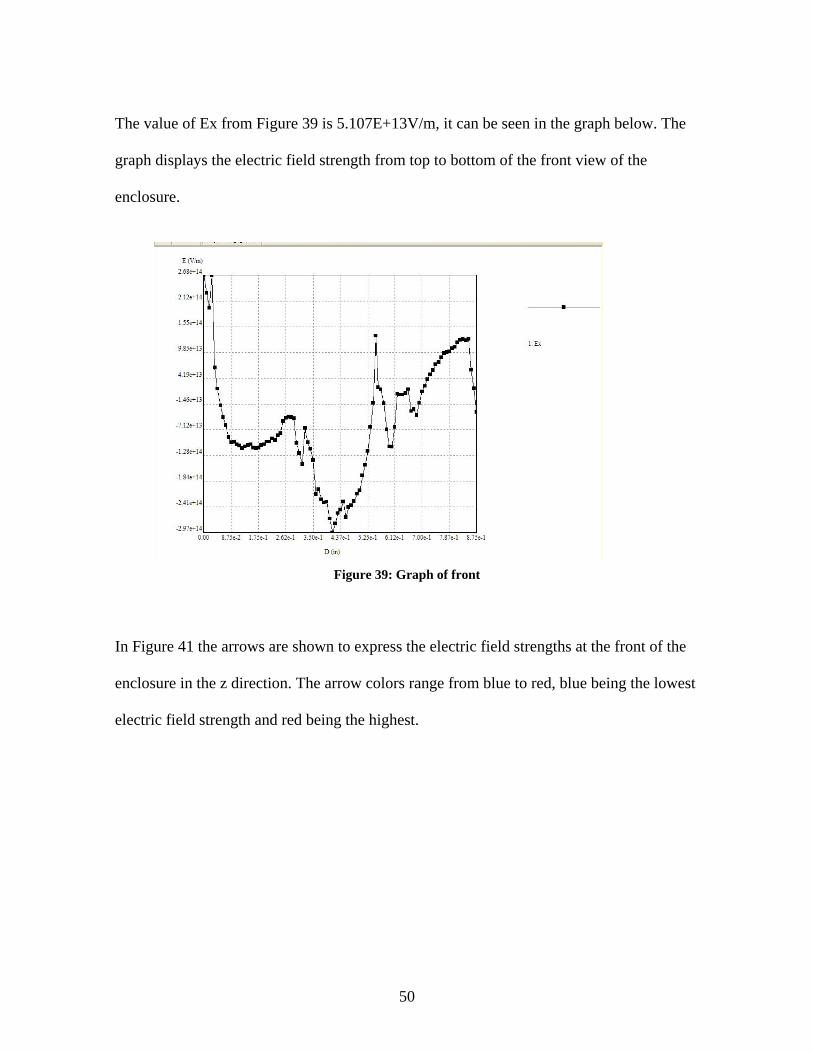
The value of Ex from Figure 39 is 5.107E+13V/m, it can be seen in the graph below. The
graph displays the electric field strength from top to bottom of the front view of the
enclosure.
Figure 39: Graph of front
In Figure 41 the arrows are shown to express the electric field strengths at the front of the
enclosure in the z direction. The arrow colors range from blue to red, blue being the lowest
electric field strength and red being the highest.

51
In Figure 42 the field analysis result is solving for the electric field at a point on any
surface. The values shown at the bottom of the screen display the electric field in the x, y
and z directions and the magnitude.
Figure 40: Arrows of electric field strength

52
The green point on the surface shows the values of the electric field that are in Figure 43
below.
Figure 42: Values from chosen point on surface
Figure 41: Chosen value on surface

53
The value of Ex from Figure 43 is 6.921E+13V/m and -4.588E+14, it can be seen in the
graph below. The graph displays the electric field strength from top to bottom of the front
view of the enclosure.
Figure 43: Graph of front
In Table 1 below the values of the aluminum and stainless steel electric field strength is
compared. Although the electric field strength does not differ by much between the
aluminum and stainless steel, the lower the electric field strength the lower the chance of a
module to be affected. Since the enclosures are both grounded the electric field will
automatically go to ground.
Impressed Field Aluminum Stainless Steel Ex -1.617E+15 5.318E+14 Ey 6.068E+14 5.107E+13 Ez -6.349E+14 6.921E+13
Table 1: Electric Field Strength of Aluminum and Stainless Steel

54
After using COULOMB I learned a lot about the software and what it can perform. The
results that were shown above are only a few solutions to what this software can solve. In
general modeling is pretending to work with a real scenario while only working an
imitation that can be performed by software tools. It is important to run tests to predict
what the outcome that can then be compared to the actual results.

55
6. Results
6.1 Introduction
The following results were provided from Westinghouse Electric Company and the testing
was conducted in New Stanton, PA. The standard used for the Electrostatic testing for the
modules was the European Standard EN61000-4-2 “Testing and Measurement Techniques
Electrostatic Discharge Immunity Test” The scope of this standard relates to the immunity
requirements and test methods for electrical and electronic equipment that are subjected to
static electricity discharge. The standard also defines ranges of the test levels and
establishes test procedures.
The test setup for ESD testing is straightforward. The equipment under test is placed over a
ground surface as shown in Figure 46, which is the ground lead. This test setup consists of
a non-conductive table standing on the ground reference plane. A horizontal coupling
plane is placed on the table. The equipment under test is isolated from the coupling plane
by an insulating support. The ground lead is kept away from the equipment under test by at
least 200mm. The distance between the ground plane and the equipment under test should
be kept 100mm from the floor and 800mm from the table-top.
The procedure of the testing includes both the contact and air discharge by using
interchangeable metal tips. For contact discharge, the pointed tip is contacted with the
testing point, and a high voltage within the units is applied to discharge to the contact
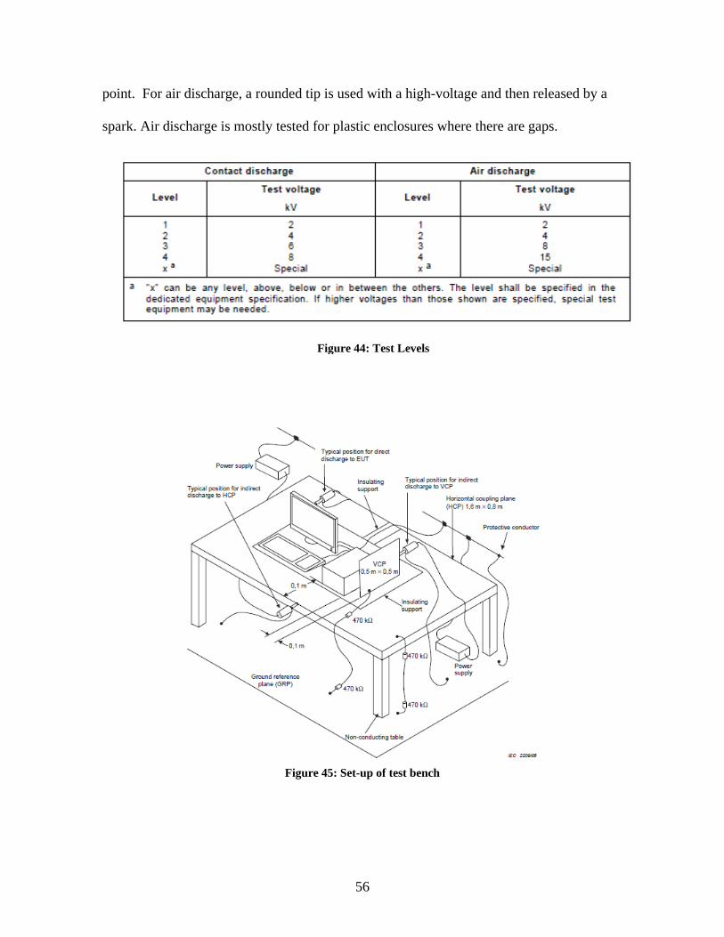
56
point. For air discharge, a rounded tip is used with a high-voltage and then released by a
spark. Air discharge is mostly tested for plastic enclosures where there are gaps.
Figure 45: Set-up of test bench
Figure 44: Test Levels

57
6.2 ESD Test Results
6.2.1 Modules
The modules supplied from Acromag are tested to a certain level without any enclosure.
According to the data sheets provided for the modules which were tested up to 4kV direct
contact and 8kV air-discharge and passed. Before the modules were tested they were
powered up and were tested for functionality. The output values of the modules were
monitored with a Fluke 2640A NetDAQ (Networked Data Acquisition Unit) data logger
and with the equipment used by the testing engineer.
Figure 46: Data Logger Software
The electrostatic discharge immunity testing began with level 1 contact and then level 1 air
discharge. The testing continues until one or more modules fail either by losing power or
not reading the expected output at the data logger. The modules did pass at level 2 for
contact and level 3 for air-discharge as noted in the data sheet. The jump to the next level

58
where contact was 8kV, where the modules all failed to read the expected output values
and a few of the modules lost power and were damaged. Since the modules were plastic
they were also tested for air-discharge at level 4 (15kV) and the modules failed.
Unfortunately the output results without the enclosures were not provided since they failed
immediately.
6.2.2 Aluminum Enclosure
The aluminum enclosure was tested with module W5207 since it’s the most common
module that is used. Since the enclosures were metal, the charge was applied by direct
contact with the metal at 8kV. The module was tested at level 1, 2 and 4 for contact
discharge. The acceptance range for this module was 117.440 – 122.560 mV.
W5207 Aluminum Enclosure Level Output Pass/Fail 2kV 120.69mV Pass 4kV 120.80mV Pass 8kV 120.74mV Pass
Table 2: Results for Aluminum
The table above shows that the enclosure designed for these modules passed testing for the
highest level of discharge.

59
6.2.3 Stainless Steel Enclosure
The same procedure was repeated for the stainless steel enclosure. The acceptance criteria
range was the same, 117.440-122.560mV.
W5207 Stainless Enclosure Level Output Pass/Fail 2kV 120.41mV Pass 4kV 120.49mV Pass 8kV 120.04mV Pass
Table 3: Results for Stainless Steel The table above shows that the enclosure design for the stainless steel also passed for the
highest level of discharge.
6.3 Compare Software and Testing Results
To evaluate the software results the electric field strength of the aluminum and stainless
steel is compared. When compared, the lower the electric field strength registers at the
enclosure, there becomes a lower chance of the module being affected. As seen in Table
1, stainless steel registers lower electric field strength across the front of the enclosure.
The testing results shown in Table 2 and Table 3 are the outputs in millivolts that are
recorded as the contact discharge is applied. The acceptance range is between 117.440 and
122.560mV. To calculate the exact expected output the mean of the values are calculated,
which is exactly 120mV. Aluminum is 0.7mV to 0.8mV higher than the exact expected
output where stainless steel is .04mV to .5mV higher than the exact expected output. This
concludes that the stainless steel was more successful than the aluminum enclosure.

60
7. Conclusions I conclude this MQP Report by summarizing the steps that were taken to complete this
project. The design of the final wiring diagram and the set up of all modules was mounted
into the cabinet. The aluminum and stainless steel enclosures were important to protect the
modules from high electrostatic discharge. The modules were only tested at medium level
and needed to pass the highest level. Numerical software was conducted to predict the field
distribution for the enclosure in orthogonal directions. The software was important to
predict if the modules would pass. The modules were then manufactured after being
designed in SolidWorks at the machine shop at Worcester Polytechnic Institute in both
aluminum and stainless steel. After the enclosures were completed they were sent down to
testing that was conducted in New Stanton, PA by Washington Labs Facility. The data
collected for the testing of the modules was then compared to the experimental results of
COULOMB.
In this project, it was successfully demonstrated that a metal enclosure can protect an
electronic device from electrostatic discharge. With the software and testing analysis that
was completed it was demonstrated that the stainless steel enclosure was more successful.
It was very important for these modules to maintain functionality at all times since they are
a crucial part to a safety system of a Nuclear Power Plant.
I suggest for any future work that may include the design of an enclosure for an electric
component that it is more carefully designed to perfectly enclose the component. Due to
limited supplies in the machine shop it was impossible to get a perfect box enclosure to not

61
have any openings or imperfections. I recommend that the enclosure is professionally
made to have a better final product that may be used in the market.

62
References
1. Hayt, William. Engineering Electromagnetics, Purdue University: 1974. 3rd Edition.
2. Marshall, Stanley, and Gabriel Skitek. Electromagnetic Concepts and Application.
New Jersey: 1990, 3rd Edition.
3. Baxleitner, Warren. Electrostatic Discharge and Electronic Equipment: A
Practical Guide for Designing to Prevent ESD Problems, Wiley-IEEE Press. 1999.
4. European Standard IEC 61000-4-2:2008, “Electromagnetic Compatibility- Part 4-2:
Testing and measurement techniques- Electrostatic Discharge immunity test” 2008.
5. Fundamentals of Electrostatic Discharge, Electrostatic Discharge Association
(Electrostatic Discharge Association, 2001)http://www.esda.org/basics/part1.cfm
6. M.A. Kelly, G.E Servais and T.V. Pfaffenbach. “An Investigation of Human Body
Electrostatic Discharge”, (Delco Electronics, 1993)
< http://www.aecouncil.com/Papers/aec1.pdf>

63
Appendix A: Standards The following are the codes and standards that direct equipment qualification of the safety-related
signal conditioning equipment.
1. IEEE Std 323-1983, “IEEE Standard for Qualifying Class 1E Equipment for
Nuclear Power Generating Stations.”
2. IEEE Std 344-1987, “IEEE Recommended Practice for Seismic Qualification of
Class 1E Equipment for Nuclear Power Generating Stations.” (Reference 7)
3. US NRC Regulatory Guide 1.29, Revision 3, “Seismic Design Classification,”
September 1978. (Reference 13)
4. US NRC Regulatory Guide 1.89, Revision 1, “Environmental Qualification of
Certain Electric Equipment Important to Safety for Nuclear Power Plants,” June 1984.
5. US NRC Regulatory Guide 1.100, Revision 2, “Seismic Qualification of Electric
and Mechanical Equipment for Nuclear Power Plants,” June 1988. (Reference 8)
6. US NRC Regulatory Guide 1.180, Revision 1, “Guidelines for Evaluating
Electromagnetic and Radio-Frequency Interference in Safety-Related Instrumentation
and Control Systems,” October 2003.
7. US NRC Regulatory Guide 1.75, Revision 2, “Physical Independence of Electric
Systems,” September 1978.
64
Appendix B: Wiring Diagrams For Each Module
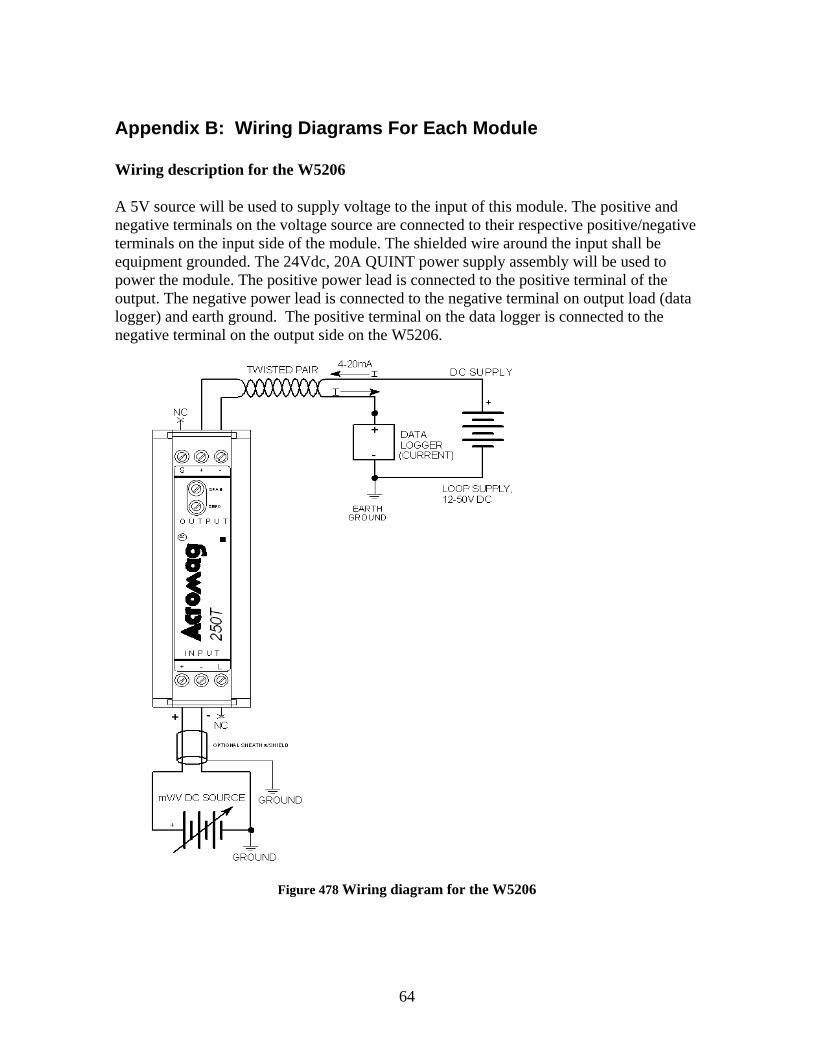
Wiring description for the W5206
A 5V source will be used to supply voltage to the input of this module. The positive and negative terminals on the voltage source are connected to their respective positive/negative terminals on the input side of the module. The shielded wire around the input shall be equipment grounded. The 24Vdc, 20A QUINT power supply assembly will be used to power the module. The positive power lead is connected to the positive terminal of the output. The negative power lead is connected to the negative terminal on output load (data logger) and earth ground. The positive terminal on the data logger is connected to the negative terminal on the output side on the W5206.
Figure 478 Wiring diagram for the W5206

65
Wiring description for the W5207
The input signal is set to 50°C using an E type thermocouple simulator. The positive and negative terminals on the thermocouple simulator are connected to their respective positive/negative terminals at the input side of the module using E type thermocouple wire (purple is positive and red is negative). The positive terminal of the module (using a short copper wire) is connected to the “L” terminal of the module. The TC break detection is already installed and in the up position, therefore the input will go high when a break is detected. The negative terminal of the thermocouple simulator is connected to instrument ground. The shielded TC wire around the input shall be equipment grounded. The 24Vdc, 20A QUINT power supply assembly will be used to power the module. The positive power lead is connected to the terminal labeled “P” on the output side. The negative power lead is connected the negative terminal of the output lead (data logger), and the negative terminal of the output side on the module, plus earth ground. The positive terminal of the output load (data logger) is connected to the positive terminal on the output side.
Figure 48 Wiring diagram for the W5207

66
Wiring description for the W5214
The input signal supplied is set to 100°C using a K type thermocouple simulator. The positive and negative terminals on the thermocouple simulator are connected to their respective positive/negative terminals at the input side of the module using K type thermocouple wire (yellow is positive and red is negative). The positive terminal of the module (using a short copper wire) is connected to the “L” terminal of the module. The TC break detection is already installed and in the up position, therefore the input will go high when a break is detected. The negative terminal of the thermocouple simulator is connected to instrument ground. The shielded TC wire around the input shall be equipment grounded. The 24Vdc, 20A QUINT power supply assembly will be used to power the module. The positive power lead is connected to the terminal labeled “P” on the output side. The negative power lead is connected to the negative terminal of the output load (data logger), and the negative terminal of the output side on the module, plus earth ground. The positive terminal of the output load (data logger) is connected to the positive terminal on the output side.
Figure 49 Wiring diagram for the W5207

67
Wiring description for the W5229
The input signal is set to 30°C using a E type thermocouple simulator. The positive and negative terminals on the thermocouple simulator are connected to their respective positive/negative terminals at the input side of the module using E type thermocouple wire (purple is positive and red is negative). Using copper wire the positive terminal is connected to the “L” terminal. The TC break detection is already installed and in the up position, therefore the input will go high when a break is detected. The negative terminal of the thermocouple simulator is connected to instrument ground. The shielded TC wire around the input shall be equipment grounded. The 24Vdc, 20A QUINT power supply assembly will be used to power the module. The positive power lead is connected to the terminal labeled “P” on the output side. The negative power lead is connected to the negative terminal of the output load (data logger), and the negative terminal of the output side on the module, plus earth ground. The positive terminal of the output load (data logger) is connected to the positive terminal on the output side.
Figure 50 Wiring diagram for the W5229

68
Wiring description for the W5216
The 2kΩ potentiometer is set to 1kΩ (midpoint). The middle lead on the potentiometer is connected to the “L” terminal. The other two leads on the potentiometer are interchangeable. One lead is connected to the positive terminal and the other is connected to the negative terminal. The negative terminal is connected to instrument ground. The shielded wire around the input shall be equipment grounded. The 24Vdc, 20A QUINT power supply assembly will be used to power the module. The positive power lead is connected to the terminal labeled “P” on the output side. The negative power lead is connected to the negative terminal of the output load (data logger), and the negative terminal of the output side of the module on the module, plus earth ground. The positive terminal of the output load (data logger) is connected to the positive terminal on the output side.
Figure 51 Wiring diagram for the W5216

69
Wiring description for the W5218
The input signal is given by the RTD simulator using the three (3) input wire configuration. The RTD simulator will be set to 26°C (110.12Ω). The negative terminal is connected to instrument ground. The shielded wire around the input shall be equipment grounded. The 24Vdc, 20A QUINT power supply assembly will be used to power the module. The positive power lead is connected to the terminal labeled “P” on the output side. The negative power lead is connected to the negative terminal of the output load (data logger), and the negative terminal of the output side on the module, plus earth ground. The positive terminal of the output load (data logger) is connected to the positive terminal on the output side.
Figure 52 Wiring diagram for the W5218
70
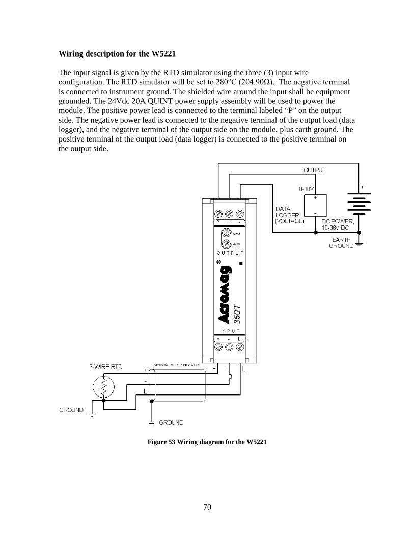
Wiring description for the W5221
The input signal is given by the RTD simulator using the three (3) input wire configuration. The RTD simulator will be set to 280°C (204.90Ω). The negative terminal is connected to instrument ground. The shielded wire around the input shall be equipment grounded. The 24Vdc 20A QUINT power supply assembly will be used to power the module. The positive power lead is connected to the terminal labeled “P” on the output side. The negative power lead is connected to the negative terminal of the output load (data logger), and the negative terminal of the output side on the module, plus earth ground. The positive terminal of the output load (data logger) is connected to the positive terminal on the output side.
Figure 53 Wiring diagram for the W5221

71
Wiring description for the W5224
The input signal is given by the RTD simulator using the three (3) input wire configuration. The RTD simulator will be set to 66°C (125.54Ω). The negative terminal is connected to instrument ground. The shielded wire around the input shall be equipment grounded. The 24Vdc 20A QUINT power supply assembly will be used to power the module. The positive power lead is connected to the terminal labeled “P” on the output side. The negative power lead is connected to the negative terminal of the output load (data logger), and the negative terminal of the output side on the module, plus earth ground. The positive terminal of the output load (data logger) is connected to the positive terminal on the output side.
Figure 54 Wiring diagram for the W5224

72
Wiring description for the W5227
The input signal is given by the RTD simulator using the three (3) input wire configuration. The RTD simulator will be set to 200°C (175.86Ω). The negative terminal is connected to instrument ground. The shielded wire around the input shall be equipment grounded. The 24Vdc, 20A QUINT power supply assembly will be used to power the module. The positive power lead is connected to the terminal labeled “P” on the output side. The negative power lead is connected to the negative terminal of the output load (data logger), and the negative terminal of the output side on the module, plus earth ground. The positive terminal of the output load (data logger) is connected to the positive terminal on the output side.
Figure 55 Wiring diagram for the W5227
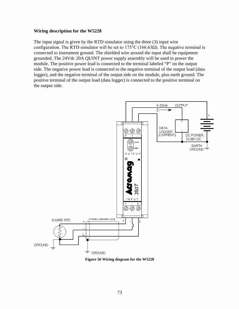
73
Wiring description for the W5228
The input signal is given by the RTD simulator using the three (3) input wire configuration. The RTD simulator will be set to 175°C (166.63Ω). The negative terminal is connected to instrument ground. The shielded wire around the input shall be equipment grounded. The 24Vdc 20A QUINT power supply assembly will be used to power the module. The positive power lead is connected to the terminal labeled “P” on the output side. The negative power lead is connected to the negative terminal of the output load (data logger), and the negative terminal of the output side on the module, plus earth ground. The positive terminal of the output load (data logger) is connected to the positive terminal on the output side.
Figure 56 Wiring diagram for the W5228

74
Wiring description for the W5204
The input signal is 12mA. The positive lead on the current source will be connected to “IN +” on the W5204. The negative lead will be connected to the “24V+” terminal. The shielded wire around the negative and positive leads on the current source shall be equipment grounded. “IN –“is tied to RTN and instrument ground. The 24Vdc, 20A QUINT power supply assembly will be used to power the module. The positive power lead is connected to a 200mA high surge fuse, which is then connected to terminal labeled “DC+” on the W5204. The negative lead is connected to earth ground and the terminal labeled “DC-“. The terminal labeled “GND” is connected to earth ground. At the output the data logger will be connected between the outputs positive and negative terminals. The negative lead on the data logger is connected to the negative output terminal. The positive lead will be connected to the positive output terminal. Input impedance to the data logger must be below.
Figure 57 Wiring diagram for the W5204
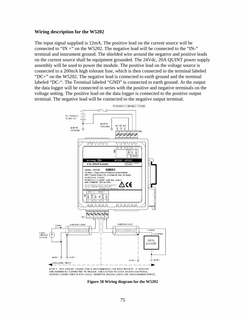
75
Wiring description for the W5202
The input signal supplied is 12mA. The positive lead on the current source will be connected to “IN +” on the W5202. The negative lead will be connected to the “IN-” terminal and instrument ground. The shielded wire around the negative and positive leads on the current source shall be equipment grounded. The 24Vdc, 20A QUINT power supply assembly will be used to power the module. The positive lead on the voltage source is connected to a 200mA high tolerant fuse, which is then connected to the terminal labeled “DC+” on the W5202. The negative lead is connected to earth ground and the terminal labeled “DC-“. The Terminal labeled “GND” is connected to earth ground. At the output the data logger will be connected in series with the positive and negative terminals on the voltage setting. The positive lead on the data logger is connected to the positive output terminal. The negative lead will be connected to the negative output terminal.
Figure 58 Wiring diagram for the W5202

76
Wiring description for the W5205
The input signal supplied is 12mA. The positive lead on the current source will be connected to “IN+” on the W5205. The negative lead will be connected to the “IN-” terminal and instrument ground. The shielded wire around the negative and positive leads on the current source shall be equipment grounded. The 24Vdc, 20A QUINT power supply assembly will be used to power the module. The positive power lead is connected to 200mA high tolerant fuse, which is then connected to the “OUT+” terminal on the W5205. The negative power lead and the negative lead on the data logger are connected to earth ground. The positive lead on the data logger is connected to the “OUT-“terminal.
Figure 59 Wiring diagram for theW5205

77
Appendix C: Test Equipment The test equipment will be used to monitor the Acromag Modules. All test equipment used during test must be in current calibration.
1. Qty. 1 Fluke 2640A/2645A NetDAQ Data Logger with accuracy of less than or equal to ± 0.025%.
2. Qty. 1 2620A-101 Current Shunt Resistors. Contains twelve (12) ten (10) +/- 0.08 % ohm resistors.
3. Qty. 1 Power supply. The power supply is set to 24Vdc and capable of drawing 3A.
4. Qty. 2 200mA High surge-tolerant fuses (318P Series 3AG Fast-Acting axial Lead Fuses).
5. Qty. 2 fuse holders (155 series twist-lock in-line type fuse holders for 3AG-SFE)
6. Qty. 1 Variable dc Voltage source. Capable of reaching 6 volts. Used to drive the input to the W5206
7. Qty. 3 Thermocouple simulators. Capable of simulating Type E and K thermocouples.
8. Qty. 3mA calibrators (Current Source)
9. Qty. 5 Resistance Temperature Detector simulators (or precision Decade Box).
10. Qty. 1 Potentiometer, 2kΩ, Capable of adjustment to 1kΩ. Accuracy +/- 1%.
11. Qty. 3 boxes of Terminal blocks. Type E thermocouple, Type K thermocouple, and regular terminal blocks.
12. Qty. 80 ft shielded twisted pair of Type E thermocouple wire.
13. Qty. 40 ft. shielded twisted pair of Type K thermocouple wire.
14. Qty. 880 ft, 3 Conductor Shielded Cable; one white, one black, and one red.
15. Qty. 3 Din Rail Kit 20.96” in length
16. Qty. 1 Digital Multimeter (DMM) for checking instruments with accuracy of equal to or less than ± 0.025%

78
Appendix D: Test Setup
1. Using a DMM, verify twelve (12) 2620A-101 Current Shunt Resistors are 10Ω +/-0.08%.
2. Place ten (10) 2620A-101 Current Shunt Resistors in shunt across the data loggers input terminals that require a current output reading.
3. Measure and set the 2kΩ potentiometer to ½ its maximum value prior to connecting to module.
4. Verify the potentiometer output is actually ½ the measured maximum value at approximately 1.00785k Ω (± 0.1 %).
5. Set the RTD simulator input for module W5218 (RTD1; Input Cable 3) to Pt 100 ohm 385 at 26°C (110.12Ω).
6. Using a DMM, verify the RTD simulator input for module W5218 is 110.12Ω.
7. Set the RTD simulator input for module W5221 (RTD2; Input Cable 4) to Pt 100 ohm 385 at 280°C (204.9Ω).
8. Using a DMM, verify the RTD simulator input for module W5221 is 204.9Ω.
9. Set the RTD simulator input for module W5224 (RTD3; Input Cable 5) to Pt 100 ohm 385 at 66°C (125.54Ω).
10. Using a DMM, verify the RTD simulator input for module W5224 is 125.54Ω.
11. Set the RTD simulator input for module W5227 (RTD4; Input Cable 6) to Pt 100 ohm 385 at 200°C (175.86Ω).
12. Using a DMM, verify the RTD simulator input for module W5227 is 175.86Ω.
13. Set the RTD simulator input for module W5228 (RTD5; Input Cable 7) to Pt 100 ohm 385 at 175°C (166.63Ω).
14. Using a DMM, verify the RTD simulator input for module W5228 is 166.63Ω.
15. Turn on the 24Vdc Power Supply Assembly.
16. Using a DMM, verify the 24Vdc output of the Power Supply Assembly.
17. Turn on 5Vdc voltage source and set to 5V.

79
18. Using a DMM, verify the voltage source output is 5Vdc (± 0.01%+3mV)
19. Set the E type thermocouple simulator input for module W5207 (TC1) consistent with 50°C.
20. Using a thermocouple calibrator, verify the thermocouple simulator input to module W5207 is 3.685mVDC.
21. Set the K type thermocouple simulator input for module W5214 (TC2) consistent with 100°C.
22. Using a thermocouple calibrator, verify the thermocouple simulator input to module W5214 is 4.509mVDC.
23. Set the E type thermocouple simulator input for module W5229 (TC3) consistent with 30°C.
24. Using a thermocouple calibrator, verify the thermocouple simulator input to module W5229 is 2.420mVDC.
25. Set the current source to “on”.
26. Using a DMM, verify the current source is supplying 12mA (± 0.01%+2 counts).
27. Turn on the data logger.
28. Make sure the inputs are on the correct setting (Voltage/Current).
29. Wire up the circuit according to pervious section.
30. With everything powered up and connected correctly wait a half an hour before beginning initial testing.
31. Test the modules and recorded in Table 10.1-1 before EMI testing.
32. Begin EMI testing; Re-test the modules and record in Table 10.1-2.
33. Shortly after EMI testing, Re-test the modules and record in Table 10.1-3.
34. Repeat steps 2, 4, 6, 8, 10, 12, 14, 16, 18, 20, 22, and 24. Record in Table 10.1-3.
Note:
1 The test equipment readings should only vary within there accuracies.

80
2 To obtain the necessary current readings take the voltage that results and divide it by ten (10)
Appendix E: Expected Outputs with Tolerances I/O Table of Acromag Modules (After Setup and Testing)
Data Logger Channel/
Westinghouse par t
number:
Manufacturer’s par t number:
Input Output Module Type Input Cable Output Cable
1.W5206 250T-V2-DIN-NCR-C 5Vdc 11.8912-12.1088mA
Voltage to Current Converter
Cable 1 Cable 11
2.W5207 350T-EL00-Y-DIN-NCR-C
50°C 11.7440-12.2560mA
TC (Type E input) to Current Converter
TC1 Cable 12
3.W5214 350T-KL00-Y-DIN-NCR-C
100°C 11.8240-12.1760mA
TC (Type K input) to Current Converter
TC2 Cable 13
4.W5229 350T-TC3-Y-DIN-NCR-C
30°C 13.016-13.892mA
TC (Type E input) to Current Converter
TC3 Cable 14
5.W5216 350T-P-Y-DIN-NCR Max / 2 Approx. 1.00785k Ω
11.8912-12.1088mA
Potentiometer/Slide wire (input) to Current Converter
Cable 2 Cable 15
6.W5218 350T-RBP1-Y-DIN-NCR-C
26°C (110.12Ω)
14.2672-14.5328mA
RTD (input) to Current Converter
Cable 3 Cable 16
7.W5221 Special 350T-RBP1-V0-DIN-NCR-C
280°C (204.90Ω)
4.94-5.06Vdc
RTD (input) to Voltage Converter
Cable 4 Cable 17
12.W5224 350T-RBP2-Y-DIN-NCR-C
66°C (125.54Ω )
11.8912-12.1088mA
RTD (input) to Current Converter
Cable 5
Cable 18
8.W5227 350T-RBP3-V0-DIN-NCR-C
200°C (175.86Ω)
4.94-5.06Vdc
RTD (input) to Voltage Converter
Cable 6 Cable 19
13.W5228 350T-RBP3-Y-DIN-NCR-C
175°C (166.63Ω)
11.8912-12.1088mA
RTD (input) to Current Converter
Cable 7 Cable 20
14.W5204 631T-0500 12mA 11.8192-12.1808mA
Current to Current Isolator
Cable 8 Cable 21
15.W5202 Special 631T-0500 (W5202)
12mA 4.895-5.105Vdc Current to Voltage Converter
Cable 9
Cable 22
16.W5205 651T-0600 12mA 11.8112-12.1888mA
Current to Current Isolator
Cable 10 Cable 23
Note: 1. TC = Thermocouple 2. RTD = Resistance Temperature Detector

81

82
Appendix F: Ideal Expected Outputs W5206 Ideal expected output
The output with accepted tolerances is given in Table 9.2-1. The Acromag W5206 module generates a current output signal (See Equation 1 below for ideal output calculation).
( )
++
×
±
+−×
=
100)( yUncertaintResistorResistanceRFIyUncertaintCombinedspanOutput
OffsetZeroOutputZeroInputInputActualSpanInputSpanOutputOutputIdeal
( ) mAmAmAmAVVVmAOutputIdeal 1088.012
100%08.0%5.0%1.016405
1016
±=
++
×±
+−×
=
Equation 1: Output Calculation for the W5206 Module
W5207 Ideal expected output
The output with accepted tolerances is given in Table 9.2-1. The Acromag W5207 module generates a current output signal (See Equation 2 below for ideal output calculation).
( )
++
×
±
+−×
=
100y)UncertaintResistorResistanceRFIyUncertaint(CombinedspanOutput
OffsetZeroOutputZeroInputInputActualSpanInputSpanOutputOutputIdeal
( ) mAmAmAmAmACCOutputIdeal 2560.012
100%08.0%5.0%02.116416
10050
±=
++
×±
+×
°°
=
Equation 2: Output Calculation for the W5207 Module
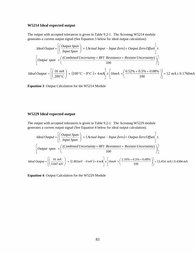
83
W5214 Ideal expected output
The output with accepted tolerances is given in Table 9.2-1. The Acromag W5214 module generates a current output signal (See Equation 3 below for ideal output calculation).
( )
++
×
±
+−×
=
100)( yUncertaintResistorResistanceRFIyUncertaintCombinedspanOutput
OffsetZeroOutputZeroInputInputActualSpanInputSpanOutputOutputIdeal
( ) mAmAmAmACCC
mAOutputIdeal 1760.012100
%08.0%5.0%52.0164010020016
±=
++
×±
+°−°×
°
=
Equation 3: Output Calculation for the W5214 Module
W5229 Ideal expected output
The output with accepted tolerances is given in Table 9.2-1. The Acromag W5229 module generates a current output signal (See Equation 4 below for ideal output calculation).
( )
++
×
±
+−×
=
100)( yUncertaintResistorResistanceRFIyUncertaintCombinedspanOutput
OffsetZeroOutputZeroInputInputActualSpanInputSpanOutputOutputIdeal
( ) mAmAmAmAmVmVmV
mAOutputIdeal 4384.0454.13
100%08.0%5.0%16.21640801.1
047.316
±=
++
×±
+−×
=
Equation 4: Output Calculation for the W5229 Module

84
W5216 Ideal expected output
The output with accepted tolerances is given in Table 9.2-1 The Acromag W5216 module generates a current output signal (See Equation 5 below for ideal output calculation).
( )
++
×
±
+−×
=
100)( yUncertaintResistorResistanceRFIyUncertaintCombinedspanOutput
OffsetZeroOutputZeroInputInputActualSpanInputSpanOutputOutputIdeal
( ) mAmAmAmAKKKmAOutputIdeal 1088.012
100%08.0%5.0%1.016401
216
±=
++
×±
+−×
=
Equation 5: Output Calculation for the W5216 Module
W5218 Ideal expected output
The output with accepted tolerances is given in Table 9.2-1 The Acromag W5218 module generates a current output signal (See Equation 6 below for ideal output calculation).
( )
++
×
±
+−×
=
100)( yUncertaintResistorResistanceRFIyUncertaintCombinedspanOutput
OffsetZeroOutputZeroInputInputActualSpanInputSpanOutputOutputIdeal
( ) mAmAmAmACCC
mAOutputIdeal 1328.04.14100
%08.0%5.0%25.01640264016
±=
++
×±
+°−°×
°
=
Equation 6: Output Calculation for the W5218 Module

85
W5221 Ideal expected output
The output with accepted tolerances is given in Table 9.2-1 The Acromag W5221 module generates a voltage output signal (See Equation 7 below for ideal output calculation).
( )
+
×
±
+−×
=
100)( ResistanceRFIyUncertaintCombinedspanOutput
OffsetZeroOutputZeroInputInputActualSpanInputSpanOutputOutputIdeal
( ) VVVCCC
VOutputIdeal 06.05100
%5.0%1.01023028010010
±=
+
×±
°−°×
°
=
Equation 7: Output Calculation for the W5221 Module
W5224 Ideal expected output
The output with accepted tolerances is given in Table 9.2-1. The Acromag W5224 module generates a voltage output signal (See Equation 8 below for ideal output calculation).
( )
++
×
±
+−×
=
100)( yUncertaintResistorResistanceRFIyUncertaintCombinedspanOutput
OffsetZeroOutputZeroInputInputActualSpanInputSpanOutputOutputIdeal
( ) mAmAmAmACCC
mAOutputIdeal 1088.012100
%08.0%5.0%1.0164186616816
±=
++
×±
+°+°×
°
=
Equation 8: Output Calculation for the W5224 Module

86
W5227 Ideal expected output
The output with accepted tolerances is given in Table 9.2-1. The Acromag W5227 module generates a voltage output signal (See Equation 9 below for ideal output calculation)
( )
+
×
±
+−×
=
100)( ResistanceRFIyUncertaintCombinedspanOutput
OffsetZeroOutputZeroInputInputActualSpanInputSpanOutputOutputIdeal
( ) VVVCCC
VOutputIdeal 06.05100
%5.0%1.010020040010
±=
+
×±
°−°×
°
=
Equation 9: Output Calculation for the W5227 Module
W5228 Ideal expected output
The output with accepted tolerances is given in Table 9.2-1. The Acromag W5228 module generates a current output signal (See Equation 10 below for ideal output calculation).
( )
++
×
±
+−×
=
100)( yUncertaintResistorResistanceRFIyUncertaintCombinedspanOutput
OffsetZeroOutputZeroInputInputActualSpanInputSpanOutputOutputIdeal
( ) mAmAmAmACCC
mAOutputIdeal 1088.012100
%08.0%5.0%1.0164017535016
±=
++
×±
+°−°×
°
=
Equation 10: Output Calculation for the W5228 Module

87
W5204 Ideal expected output
The output with accepted tolerances is given in Table 9.2-1. The Acromag W5204 module generates a current output signal (See Equation 11 below for ideal output calculation).
( )
++
×
±
+−×
=
100)( yUncertaintResistorResistanceRFIyUncertaintCombinedspanOutput
OffsetZeroOutputZeroInputInputActualSpanInputSpanOutputOutputIdeal
( ) mAmAmAmAmAmAmAmAOutputIdeal 1808.012
100%08.0%1%05.0164412
1616
±=
++
×±
+−×
=
Equation 11: Output Calculation for the W5204 Module
W5202 Ideal expected output
The output with accepted tolerances is given in Table 9.2-1. The Acromag W5202 module generates a voltage output signal (See Equation 12 below for ideal output calculation).
( )
+
×
±
+−×
=
100)( ResistanceRFIyUncertaintCombinedspanOutput
OffsetZeroOutputZeroInputInputActualSpanInputSpanOutputOutputIdeal
( ) VVVmAmAmAV
OutputIdeal 105.05100
%1%05.0104121610
±=
+
×±
−×
=
Equation 12: Output Calculation for the W5202 Module

88
W5205 Ideal expected output
The output with accepted tolerances is given in Table 9.2-1. The Acromag W5205 module generates a current output signal (See Equation 13 below for ideal output calculation).
( )
++
×
±
+−×
=
100)( yUncertaintResistorResistanceRFIyUncertaintCombinedspanOutput
OffsetZeroOutputZeroInputInputActualSpanInputSpanOutputOutputIdeal
( ) mAmAmAmAmAmAmAmAOutputIdeal 1888.012
100%08.0%1%1.0164412
1616
±=
++
×±
+−×
=
Equation 13: Output Calculation for the W5205 Module