elsevier editorial system(tm) for journal of magnetism and
TRANSCRIPT

Elsevier Editorial System(tm) for Journal of Magnetism and Magnetic Materials Manuscript Draft Manuscript Number: MAGMA-D-13-01129R1 Title: Magnetism Variations and Susceptibility Hysteresis at the Metal-Insulator Phase Transition Temperature of VO2 in a Composite Film Containing Vanadium and Tungsten Oxides Article Type: Regular Submission Corresponding Author: Dr. Bonex Wakufwa Mwakikunga, PhD Corresponding Author's Institution: Council for Scientific and Industrial Research First Author: Bonex Wakufwa Mwakikunga, PhD Order of Authors: Bonex Wakufwa Mwakikunga, PhD; Amos A Akande, MSc; Erasmus K Rammutla, PhD(Physics); Thomas Moyo, PhD; Nadir S Osman, MSc; Steven S Nkosi, MSc; Charl Jafta, PhD Abstract: We report on the magnetic property of 0.67-WO3 + 0.33-VOx mixture film deposit on the corning glass substrate using chemical sol gel and atmospheric pressure chemical vapour deposition (APCVD) methods. The XRD and Raman spectroscopy confirm species of both materials, and the morphological studies with FIB-SEM and TEM reveal segregation of W and V atoms. XPS reveals that V4+ from VO2 forms only 11% of the film; V3+ in the form of V2O3 form 1% of the film, 21% is V5+ from V2O5 and 67% is given to W6+ from WO3. The analysis of the ESR data shows some sharp changes in the magnetism near the MIT, which could be theoretically interpreted as the ordering or alignment of electron spins from net moment nature to parallel alignment of magnetic moment. The derivatives of magnetic susceptibility established the thermally induced magnetic property:- two distinct transitions of 339 K for heating data and 338 K for cooling data for 151.2 mT field were obtained. Similar results were also obtained for 308.7 mT field, 336 K for heating data and 335 K for cooling data.VSM results confirm a paramagnetic phase with a small amount of magnetically ordered phase.

DST/CSIR National Centre for Nano-Structured Materials, PO Box 395,
Pretoria 0001, South Africa
To: Editor, Journal of Magnetism and Magnetic Materials
Attention to: Prof S Bader
Date: 22nd
July, 2014
Dear Editor
Subject: Re-vision and re-submission of article “Magnetism Variations and Susceptibility
Hysteresis at the Metal-Insulator Phase Transition Temperature of VO2 in a Composite
Containing Vanadium and Tungsten Oxides”
On behalf of all authors, I am happy to submit the above revised manuscript to your journal. We
confirm that the manuscript has been duly revised and all the suggestions made by the reviewer have
been considered accordingly.
We look forward to your consideration to publish our paper.
Yours sincerely,
Bonex Mwakikunga, PhD(Wits 2009), MSc (Wits 2006), BEdSc(Hons) (Malawi
1994), BEdSc(Malawi 1992)
Principal Research (Nano Physics)
Contact: 012 841 3784 or Mobile 084 211 7844
Cover Letter
Ms. Ref. No.: MAGMA-D-13-01129
Title: Paramagnetism and Susceptibility Hysteresis Near the Metal - Insulator Phase Transition Temperature of Heavily
Tungsten-Doped Vanadium Dioxide
Journal of Magnetism and Magnetic Materials
Dear Bonex,
The reviewer has now commented on your paper. You will see that he/she is advising that you revise your manuscript.
If you are prepared to undertake the work required, I would be pleased to reconsider my decision.
For your guidance, the reviewer's comments are appended below.
If you decide to revise the work, please submit a list of changes or a rebuttal against each point which is being raised
when you submit the revised manuscript.Your revised manuscript should be submitted within one month. If you do
not do so, we will assume that you do not wish to submit a revised version and your manuscript will be withdrawn
from consideration.
To submit a revision, please go to http://ees.elsevier.com/magma/ and login as an Author.
Your username is: [email protected]
If you need to retrieve password details, please go to:
http://ees.elsevier.com/magma/automail_query.asp
NOTE: Upon submitting your revised manuscript, please upload the source files for your article. For additional details
regarding acceptable file formats, please refer to the Guide for Authors at: http://www.elsevier.com/journals/journal-
of-magnetism-and-magnetic-materials/0304-8853/guide-for-authors
When submitting your revised paper, we ask that you include the following items:
Manuscript and Figure Source Files (mandatory)
We cannot accommodate PDF manuscript files for production purposes. We also ask that when submitting your
revision you follow the journal formatting guidelines. Figures and tables may be embedded within the source file for
the submission as long as they are of sufficient resolution for Production.For any figure that cannot be embedded
within the source file (such as *.PSD Photoshop files), the original figure needs to be uploaded separately. Refer to the
Guide for Authors for additional information.
http://www.elsevier.com/journals/journal-of-magnetism-and-magnetic-materials/0304-8853/guide-for-authors
Highlights (mandatory)
Highlights consist of a short collection of bullet points that convey the core findings of the article and should be
submitted in a separate file in the online submission system. Please use 'Highlights' in the file name and include 3 to 5
bullet points (maximum 85 characters, including spaces, per bullet point). See the following website for more
information
http://www.elsevier.com/highlights
Graphical Abstract (optional)
Graphical Abstracts should summarize the contents of the article in a concise, pictorial form designed to capture the
attention of a wide readership online. Refer to the following website for more information:
http://www.elsevier.com/graphicalabstracts
On your Main Menu page is a folder entitled "Submissions Needing Revision". You will find your submission record
there.
*Response to Reviewers

Please note that this journal offers a new, free service called AudioSlides: brief, webcast-style presentations that are
shown next to published articles on ScienceDirect (see also http://www.elsevier.com/audioslides). If your paper is
accepted for publication, you will automatically receive an invitation to create an AudioSlides presentation.
Yours sincerely,
Samuel D. Bader
Editor
Journal of Magnetism and Magnetic Materials
Reviewer's comments:
The article deals with observed magnetic property changes in heavily W-doped VO2 sol-gel deposits, which is a topic
of considerable interest to the VO2 community. Materials characterization and ESR measurements were reported with
due diligence. This paper should be published in JMMM only after the following points are addressed:
I have few main concerns, which if our authors can clarify/address, would be good:
1) The preparation and characterization of the deposit does not convince me if at all W-doping of VO2 was
achieved…from the TEMs in Fig.5 it is hard to say if there is a region where there is "VO2" doped with
W…it is not very clear if the region that was scanned has VO2 as well as W. Also, the amount of W-
doping in percentage or concentration, which is necessary, has not been stated anywhere in the paper.
The XRD in figure 3 can be taken by a large spot that encompasses both the "VO2" and the "W" areas
next to each other. Same for the Raman Spectrum in figure 4. The hysteresis curves in figure 6 are
generated only in the "VO2" area, hence leaving no scope for verifying the known fact that W-doping
reduces the transition temperature of VO2. Hence, it hasn't been convincingly addressed if VO2 has
been successfully doped by W or not. Authors are requested to point out a proof of W-doping and
provide a semi-quantitative estimate of how much W-incorporation has happened to make this study
useful.
Authors’ response: Thank you. The reviewer is correct. In order to verify the alleged W-doping, we have
carried x-ray photoelectron spectroscopy (XPS). It is found that 67% if the film is W6+
most likely from
the WO3 phase and then 33% is from vanadium oxides. Therefore this is not heavily W-doped film as we
concluded before. This is equivalent to alloying. In fact the tungsten oxide phases separate themselves
from the vanadium oxide phases in a process called segregation. XPS confirms Raman spectroscopy and
XRD that WO3 and V2O5 seem to be predominant. We have presented XRD, Raman spectroscopy and
XPS in Figure 3 of the revised manuscript and their discussion is on Page 13 and 14.
2) It is very important to make pure VO2 to study the phase transition behavior. It seems like the sample in
question had VO2 (M1 as well as B) and V2O5 , this makes the result interpretation a little complex. VO2
(B) has been reported in literature to have a different transition temp. (see Corr et al, Journal of Materials
Chemistry, 2009 , 19, 4362-4367, and reference 8 and 9 in that paper, which refers to Oka et al - the
magnetic property of VO2(B) has been reported in these as well. ) Hence, the change of mag. property
observed in this manuscript might not be attributable to W-doping.
Authors’ response: Thank you again for this observation. Although this film has WO3 and VOx phases,
the 33% proportion ascribed to the VOx phases is further subdivided in accordance with XPS analysis as
follows: 11% to VO2 and 22% to V2O5. In the temperature range considered (300-353 K) only the VO2 M1
transition can be observed. The rest of the phases have transitions beyond this range; for instance VO2
B or VO2 A have transitions above 120 deg C (393 K) or 150 deg C (423K), WO3 at 200 deg C (473 K),
V2O5 at 375 deg C (648K). This description is included in the revised manuscripts and indeed we have
read and cited the suggested papers as follows:
Corr et al is already cited in Ref. 41
Ref [51] F. Theobald, R. Cabala, J. Bernard, Test on the structure of VO2(B), J. Solid State Chem., 17 (1976)
431
Ref [52] Y. Oka, T. Yao, N. Yamamoto, Y. Ueda, A. Hayashi, Phase transition and V4+
-V4+
pairing in VO2(B),
J. Solid State Chem. 105 (1993) 271
3) The ESR data d/dt, does not really tell us whether it is para, ferro or ferrimagnetic, it only indicates a
change. We need the full susceptibility curve (T) and M vs H hysteresis curve before and after transition
to show that there is ferromagnetism after transition. Otherwise, the abstract and discussion needs to be
modified to say only that, there is a change in magnetic susceptibility during transition, and it can be
used to track the transition itself, as is correctly pointed out in the conclusion section.
Authors’ response: The reviewer is correct. Some authors on ESR have ascribed sharp ESR line-shapes to
para-magnetism and broad ESR line-shapes to ferro-magnetism []. This argument is based on the fact
that ESR is in fact sometimes referred to as EPR (electron paramagnetic resonance) and therefore sharp
and intense resonances are ascribed to para-magnetism. However other authors [] on ESR have
explained sharp or broad as ferro or para respectively to the contrary; this difference in opinions shows
that the use of the nature of the ESR line-shapes to ferro or ferri and para magnetism is not ye resolved
in ESR.
In order to ascertain the para or ferro magnetism in this film, we have undertaken Vibrating Sample
Magnetometry (VSM) in order to obtain M vs H hysteresis curves. We have obtained M vs H hysteresis
curves from a commercial and pure VO2 samples. Their degrees of para-magnetism and ferro-
magnetism are now discussed on Page 16 of the revised manuscript and the results are presented in Fig
6 (c and d).
Title, introduction, references, figures and data presentation is satisfactory. The abstract, results and discussions
sections need a little bit of work.
Title has slightly changes to reflect the corrections in the manuscript.
I would recommend this article for publication with certain revisions for enhancing the readability of this article:
Thank you.
1) Section1: Page 4 , third paragraph, last sentence needs to be revised - optical probing generally give
electronic information and not structural, and this sentence is not supported by any references either.
Corrected, thank you.
2) There are some omitted words and grammatical mistakes in phrasing sentences all through the draft. If
authors can please revise the draft accordingly that would be great. Some of them are pointed out here:
Corrected, thank you.
a) Section 2.3: Last sentence missing the mathematical quantities.
Corrected, thank you
b) Last paragraph in Section 4 before Conclusion which starts with Hysteresis in paramagnetic ____ (missing
word) and susceptibility…". Next sentence : "One leads to the fact", Last sentence: crystallite "size"
decrease - "size" word is missing.
Corrected. Thank you.
Highlights for Magnetism Variations and Susceptibility Thermal Hysteresis at the Metal-
Insulator Phase Transition of VO2 in Composite Containing Vanadium and Tungsten
Oxides by A. A. Akande1, 2, K. E. Rammutla2, T. Moyo3, N. S-E. Osman3, S. S. Nkosi4, C. Jafta5,
B. W. Mwakikunga1,1
1. Variations in magnetism of VO2 derived from electron spin resonance data at various
temperatures is employed in observing the metal-to-insulator transition (MIT)
temperature in VO2
2. Magnetization obtained from the inverse of the ESR intensity of the characteristic
peaks in the field sweeps yields novel shapes of the hysteresis loops.
3. Susceptibility derived from the paramagnetic signature confirms the VO2 MIT at 340
K.
4. Hysteresis loop width from susceptibility is just about 1 K whereas the conductivity
hysteresis loop is more than 30 K for a crystallite size of 14 nm in VO2.
5. The study reveals that the magnetic property display opposite hysteresis shapes to
any other properties (optical, electrical, roughness, surface plasmon resonance) used
to study the VO2 MIT so far.
1Author to whom correspondence is to be addressed:
Bonex Mwakikunga Email address: [email protected] Fax: +27 12 841 2229
*Highlights (for review)
Magnetism Variations and Susceptibility Hysteresis at the Metal-Insulator Phase
Transition Temperature of VO2 in a Composite Film Containing Vanadium and Tungsten
Oxides
Amos A Akande1, 2
, Koena E Rammutla2, Thomas Moyo
3, Nadir S E Osman
3, Steven S Nkosi
4,
Charl Jafta5, Bonex W. Mwakikunga
1,*
1DST/CSIR National Centre for Nano-Structured Materials, P O Box 395, Pretoria 0001, South
Africa
2University of Limpopo, Department of Physics, P/Bag X1106, Sovenga, 0727, RSA
3School of Chemistry and Physics, University of KwaZulu-Natal, Westville Campus, Durban,
South Africa
4CSIR National Laser Centre, P O Box 395, Pretoria 0001, South Africa
5CSIR Energy and Materials, CSIR P O Box 395, Pretoria 0001, South Africa
Abstract
We report on the magnetic property of 0.67-WO3 + 0.33-VOx mixture film deposit on the
corning glass substrate using chemical sol gel and atmospheric pressure chemical vapour
deposition (APCVD) methods. The XRD and Raman spectroscopy confirm species of both
materials, and the morphological studies with FIB-SEM and TEM reveal segregation of W
*Author to whom correspondence is to be addressed:
Bonex Mwakikunga Email address: [email protected] Fax: +27 12 841 2229
*ManuscriptClick here to view linked References
and V atoms. XPS reveals that V4+
from VO2 forms only 11% of the film; V3+
in the form of
V2O3 form 1% of the film, 21% is V5+
from V2O5 and 67% is given to W6+
from WO3. The
analysis of the ESR data shows some sharp changes in the magnetism near the metal-to-
insulator (MIT), which could be theoretically interpreted as the ordering or alignment of
electron spins from net moment nature to parallel alignment of magnetic moment. The
derivatives of magnetic susceptibility established the thermally induced magnetic property:-
two distinct transitions of 339 K for heating data and 338 K for cooling data for 151.2 mT
field were obtained. Similar results were also obtained for 308.7 mT field, 336 K for heating
data and 335 K for cooling data. VSM results confirm a paramagnetic phase with a small
amount of magnetically ordered phase.
Key words: Vanadium dioxide, Tungsten oxide, Metal-to-Insulator Transition,
Paramagnetism, Magnetic susceptibility.
1.0 Introduction
Vanadium forms a variety of binary oxide families which are generally expressed as follows;
VnOn, VnO2n, VnO2n-1 and VnO2n+1, with VO, V2O3, VO2, V6O13 and V2O5 being part of the
daughters raised by these families. These oxides have been given much attention by many
researchers because of their ability to exhibit metal-insulator phase transition (MIT) as
observed by Magneli, Morin, Goodenough, Adlar, Paquet, Fujimori, Peirels and Mott-
Hubbard [1-11].

Among these oxides of vanadium, VO2 with V4+
oxidation state and 3d1 configuration differs
from others in its MIT properties. The MIT in VO2 takes place at around 340 K, a
temperature close to room temperature, and this is usually accompanied by a slight shift in
its lattice structural transition from tetragonal structure (R) high temperature phase (T ≥ 340
K) to monoclinic structure (M1) low temperature phase (T< 340 K) [1],[12-13].
This structural transition has been reported to be responsible for abrupt changes in the
electrical, optical and magnetic properties [14-15], although there has not been any detailed
report on the magnetic property of VO2 MIT. This oxide is applied in various technologies;
the major being in the thermochromic applications for instance its thermally induced
electrical property is employed in the sensing of gases and chemicals [16-17]. Much
research has been done in the area of optoelectronics such as switchable window
applications and it was reported that VO2 blocks or reflects near infrared radiation in the
metallic phase and allows it in the monoclinic (semi conducting/insulating) phase [18]. Other
researchers have also reported the doping of tungsten metal ion into the lattice of VO2 in
order to enhance optical performance and possibly reduce the phase transition to room
temperature [17, 19-21].
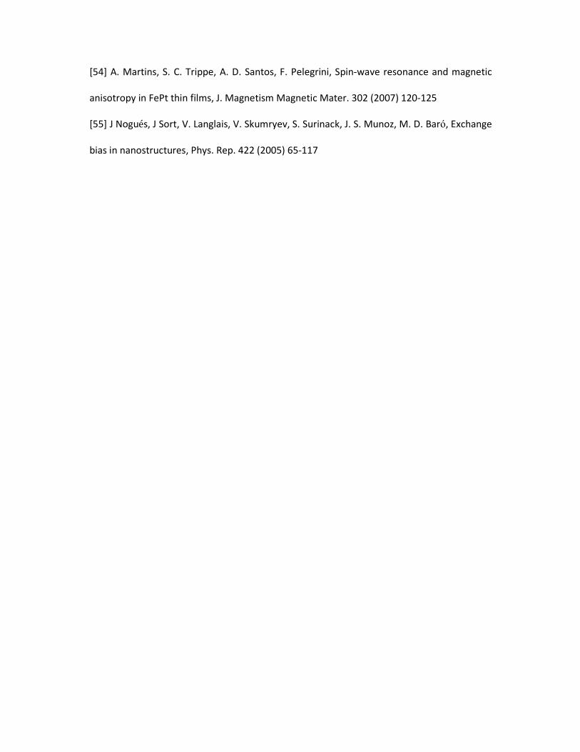
The underlying principles that explained the transitions in VO2 in great detail is the
electronic band structure and was described by Goodenough Model as presented in Fig. 1
that the vanadium (V4+
and 3d) atom in the metallic R phase (with t2g levels in the octahedral
crystal field) splits into two levels d11 and * orbital comprising the electronic states near
Fermi level of the metallic states. The d11 orbital which is nonbonding together with *
strongly hybridized with the oxygen O 2p ∗state and consequently* lie in a higher level
than d11. Insulating monoclinic phase is different in that the pairing of the V4+
atom along Cr
axis pushes the 3d-2p hybridization and up-shifts the * band away from the Fermi level
and causing the bonding and anti-bonding splitting of the d11 which is classified as the
opening of band or band gaps [1], [22].
The hysteresis thermal profile of VO2 has been studied by many scientists by measuring the
structural, morphological, electronic and optical properties at varying temperatures as
summarized in Fig. 2. Common results of hysteresis steps have been obtained when heating
up and cooling down measurements are conducted [23-24]. Fig. 2 (a) and 2 (b) show the
opposite effects or relationships with temperature for electrical resistance and conductance
S and optical transmittance and reflectance, as we know from the basic definition that
conductance S is inverse of resistance and similarly for reflectance and transmittance
(especially when the optical absorption remain constant – Beer Lambert law). Fig. 2 (c) and 2
(d) speaks of the surface effect near the MIT while Fig. 2 (e) is the Raman study of the
phonon frequency and Fig. 2(f) the effect of surface plasmon resonance wavelength near
MIT.
The electronic (resistance and or conductance) property of VO2 was explained by
Goodenough as illustrated above Fig. 1, the electrostatic consideration for the effective
ionic charges (electron to electron interaction) using anti-ferro-electric as potential driving
force for the MIT.
From this explanation, a number of experiments have been conducted [21-22] [24] and it
was found that the reason for MIT in VO2 may be due to the electron to electron interaction
between the two ions of vanadium and oxygen. Optical studies of VO2 property
(transmittance and or reflectance) [21-24] also explained the switching from monoclinic
structure (insulating) to tetragonal (metallic) structure as a function of temperature.

The transition in VO2 is thought to occur due to the effect of lattice distortion (lattice atomic
arrangement) and electronic band structure; it follows that the low-temperature monoclinic
(insulating) phase may exhibit high refractive index, and thus allow huge amount of near-
infrared radiation while high-temperature tetragonal (metallic) phase may have low
refractive index and thereby blocking this radiation [25-26].
Recently Lopez et al [12] [27] and Lysenko et al [28] also presented the thermal hysteresis
profile study of VO2 using the Fig. 2 (c) surface roughness (mm) and Fig. 2 (d) scattering
(arbitrary unit) of time-resolved light and X-ray diffraction. The MIT in VO2 is said to be
related to the nucleation mechanism of VO2 crystal [27] and the hysteresis profile of the
scattering intensity shows unique changes revealing non-linear absorption characteristic in
VO2 [28].
Phonon studies from Raman spectra have been used to explain the MIT transition of VO2
and were done by comparing the modes (vibrational, rotational, or stretching) of the room
temperature ambient pressure Raman spectrum with the spectrum at transition
temperature [29-32]. In these studies, the 617 cm-1
phonon known as the characteristic
wavenumber (although with slight variation depending on the particle size) produced
reduced relative intensity near the MIT [23]. This method has shown some convincing
thermal hysteresis profile of VO2 from various experiments as the results show emergence
of shifting in phonon frequency or relative intensity from low temperature monoclinic
(insulator) phase to high temperature tetragonal (metallic) phase [23-24].
Also recently Maaza et. al. [33] presented the thermally induced tunability of surface
plasmon resonance property of VO2 with the aim of producing VO2 nano-photonics device.
The electron resonance effect occurs when the frequency of the photon matches the
natural frequency of the surface electrons in the material, for VO2, huge shift in surface
plasmon resonance wavelength was observed in Fig. 2 (f) from insulating state to metallic
state.
In the present work, we begin by confirming the MIT of the present VO2 containing samples
by the traditional method of monitoring its conductivity as function of temperature. Once
confirmed that the MIT at 340 K is presence then we move to new properties – magnetism
changes around the VO2 MIT and sharp changes in the magnetic susceptibility.
VO2 is known to be a paramagnetic material with unpaired electrons, which have electronic
structure that leaves electron in a state in such a way that it does not have a partner of
opposite spin. Most transition metals have this magnetic behaviour as they possess surface
free standing clusters or centres and this has become of great interest as there is a
possibility for ferromagnetism in low-dimensional paramagnetic materials [34].
Imada et al [1] and reference therein presented the first magnetic studies of VO2
theoretically and experimentally by using NMR and EPR, it was discovered that the M1 phase
(ground state) is nonmagnetic with the vanadium atoms both paired and twisted from the
rutile position. They observed the emergence of other phases, namely, monoclinic, M2 and
triclinic, T, at higher temperature before reaching the transition temperature, these phases
show some magnetic charge ordering as S = ½ Heisenberg chains. The M2 transition is seen
as Mott-Hubbard insulator while T is regarded as the spin Peierls insulator although the
transition between M2 and T is a weak first order transition [1, 11].
Akoh et al. [35] also have proved experimentally that the vanadium atom which is
paramagnetic shows some existence of magnetism. They further stressed that the isolated

or structured atom of vanadium have a permanent magnetic moment of 3 µB, whereas, the
bulk vanadium atom does not exhibit any magnetic property. The magnetic property of over
layered systems of vanadium atom with tungsten has also been considered and the results
show the enhancement of magnetic property of vanadium by the hybridization of V and W
d-bands [36].
2.0 Theoretical considerations
2.1 Mott theory of MIT in insulating or polycrystalline material
N.F Motts in 1968 proposed a model for DC electrical conductivity in multi-phase or
disordered systems such as amorphous materials, compounds and alloys and polycrystalline
semiconductor systems at varying temperatures [40]. In his theory, electrical conduction is
considered in terms phonon assisted or phonon-mediated hopping of electrons from one
localized state (cat-ionic state or site) to another within the band gaps of disorder systems.
The electron hopping occurs between states of low thermal energy to states of higher
energy, Mott pointed out that the charge transport could also be as a result of the
tunnelling process whereby the electron hops from one state to another that has equal
energy or from a higher energy to a state of lower energy with the release or emission of
phonons.
The term Variable Range Hopping (VRH) is explained in the light of the characteristic
hopping length and thermal activation energy between cationic states or sites. Mott’s
model thus generally states that the electron conductivity is given as:
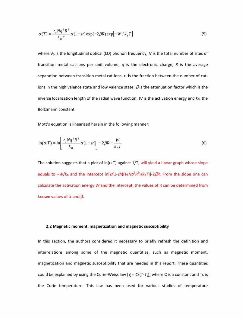
[ ]TkWRTk
RNqT B
B
/exp)2exp()1()(22
0 −−−= βαανσ (5)
where ν0 is the longitudinal optical (LO) phonon frequency, N is the total number of sites of
transition metal cat-ions per unit volume, q is the electronic charge, R is the average
separation between transition metal cat-ions, α is the fraction between the number of cat-
ions in the high valence state and low valence state, β is the attenuation factor which is the
inverse localization length of the radial wave function, W is the activation energy and kB, the
Boltzmann constant.
Mott’s equation is linearized herein in the following manner:
Tk
WR
k
RNqT
BB
−−
−= βαανσ 2)1(ln).ln(
220 (6)
The solution suggests that a plot of ln(σ.T) against 1/T, will yield a linear graph whose slope
equals to –W/kB and the intercept ln[α(1-α)(ν0Nq2R
2)/kBT]-2βR. From the slope one can
calculate the activation energy W and the intercept, the values of R can be determined from
known values of α and β.
2.2 Magnetic moment, magnetization and magnetic susceptibility
In this section, the authors considered it necessary to briefly refresh the definition and
interrelations among some of the magnetic quantities, such as magnetic moment,
magnetization and magnetic susceptibility that are needed in this report. These quantities
could be explained by using the Curie-Weiss law [χ = C/(T-Tc)] where C is a constant and Tc is
the Curie temperature. This law has been used for various studies of temperature
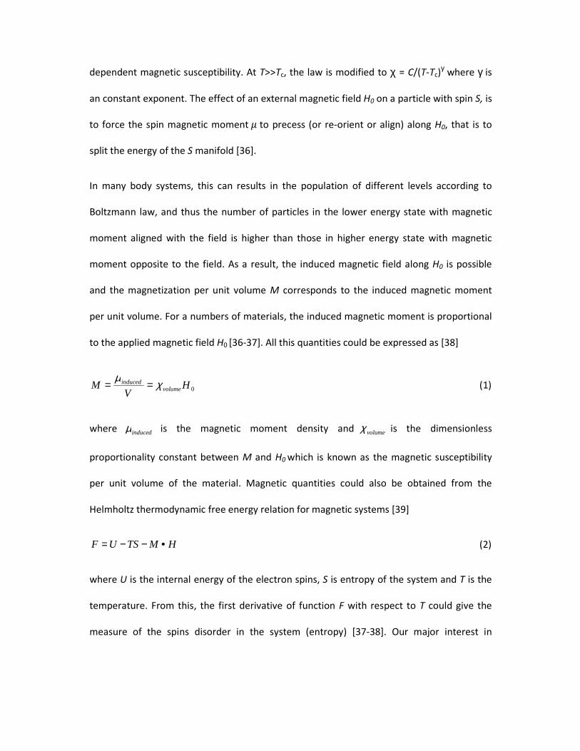
dependent magnetic susceptibility. At T>>Tc, the law is modified to χ = C/(T-Tc)γ where γ is
an constant exponent. The effect of an external magnetic field H0 on a particle with spin S, is
to force the spin magnetic moment to precess (or re-orient or align) along H0, that is to
split the energy of the S manifold [36].
In many body systems, this can results in the population of different levels according to
Boltzmann law, and thus the number of particles in the lower energy state with magnetic
moment aligned with the field is higher than those in higher energy state with magnetic
moment opposite to the field. As a result, the induced magnetic field along H0 is possible
and the magnetization per unit volume M corresponds to the induced magnetic moment
per unit volume. For a numbers of materials, the induced magnetic moment is proportional
to the applied magnetic field H0 [36-37]. All this quantities could be expressed as [38]
0HV
M volumeinduced χµ
== (1)
where inducedµ is the magnetic moment density and volumeχ is the dimensionless
proportionality constant between M and H0 which is known as the magnetic susceptibility
per unit volume of the material. Magnetic quantities could also be obtained from the
Helmholtz thermodynamic free energy relation for magnetic systems [39]
HMTSUF •−−= (2)
where U is the internal energy of the electron spins, S is entropy of the system and T is the
temperature. From this, the first derivative of function F with respect to T could give the
measure of the spins disorder in the system (entropy) [37-38]. Our major interest in
[Equation (2)] is the quantity M.H which represents magnetic energy, the negative of the
first derivative of the function will gives magnetisation M as expressed as [39]
MH
F =∂∂− (3)
Taking the derivative of [Equation (3)] with respect to H, we have the magnetic susceptibility
[39]
χ=∂∂−
H
F2
2
(4)
From the previous experimental reports, thermodynamic quantities are known to grow
rapidly in the vicinity of phase transition or have a step-wise change at Tc. This transition
could be first, second or third order derivatives of the free energy function and the
paramagnetic to ferromagnetic phase transition are a second order of magnetic
susceptibility [38-39].
2.3 Electron Spin Resonance Techniques
Electron spin resonance (ESR) is a spectroscopic technique that depends upon the property
that any atomic system with unpaired electrons possesses a net magnetic moment which
will interact with the external magnetic field. For the case of free atom containing a single
unpaired electron, the electron has one of the two possible spin directions, corresponding
to the allowed values of the spin quantum numbers ( S = - ½ or +½ ). The energies of the two
spin states are equal in the absence of magnetic field while their energies reduced and
increase respectively by ½(gβH) as the magnetic field is applied where β = eђ/2mc called
Bohr magnetron and g is the spectroscopic Zeeman splitting factor with a value of 2.0023
for a free electron [38].
3.0 Experimental
The study’s initial material consists of ammonium meta-vanadate [NH4VO3. 6H2O] and
ammonium meta-tungstate [(NH4)6W7O24.6H2O] which were in hydrate form. The [NH4VO3.
6H2O] is a whitish powder with molecular weight of 116. 98 a.m.u and density of 2.3 g cm-3
,
its melting temperature is 200 0C while [(NH4)6W7O24.6H2O] is a white trace metal basis
powder of molecular weight 2972.0 a.m.u, solubility of 0.1 g mol-1
and melting temperature
of 700 0C.
These materials were dissolved gently in equal ratio in distilled water using magnetic stirring
method with heater temperature raised to about 70 0C for 15 hours to make our precursor.
The substrate (corning glass) was cleaned several times by suspending them into glass test
tube containing distilled water and agitated in ultrasonic wave water bath for about 10
minutes each times and at 30 0C. The traditional sol gel dip coating technique was employed
to ensure that the gel-precursor sticks to the glass substrate; this substrate was then dipped
into the precursor and exposed to the atmosphere at room temperature for 72 hours. The
outcome was thick film deposits, and annealing was performed at 700 0C in APCVD reactor
under the influence of 15L min-1
hydrogen gas for 2 hrs.
The X-Ray diffraction scans were carried out using Panalytical X’ pert Pro PW 3040/60 X-Ray
diffractometer equipped with Cu Kα (λ=0.154nm) monochromatic radiation source. The

measurements were extracted at 45.0 kV and 40.0 mA, and the experimental procedure
shows a good reproducibility of results.
Topographical study and elemental composition were carried out using JOEL 2100
Transmission electron microscopy (TEM) (from Tokyo Japan) equipped with LaB6 filament
and a Gartan U1000 camera with 2028 × 2028 pixels, with high quality inbuilt Energy
dispersive X-ray spectroscopy, this was used to study the lamellar layer of the VO2 thin film
mixed with tungsten and deposited on copper grid prepared using focussed ion beam
scanning electron microscopy (FIB-SEM).
The electrical measurements were performed using the KEITHLEY 4200 Semiconductor
Characterization Systems (SCS) with a collinear four point probe system and four supply-
and-measure unit (SMU), all from Cascade Microtech, Inc., Oregon U.S.A. The film average
resistance for -30 V to +30 V voltage sweeps from below room to above transition
temperature (heating cycle) were measured using IKA® RCT basic laboratory heater. The
cooling cycle forms of these measurements were also considered.
Raman spectroscopy was conducted using a Jobin–Yvon T64000 Raman spectrograph with a
514.5 nm line from an argon ion laser. The power of the laser at the sample was small
enough (0.384 mW) in order to minimise localised heating of the sample. The T64000 was
operated in single spectrograph mode, with the 1800 lines/mm grating and a 100× objective
on the microscope.
The magnetic characterization was conducted using JOEL (JES-FA 200) ESR Spectrometer
equipped with X-band (8-12 GHz) microwave and liquid helium variable temperature
systems. The sample was prepared by targeting the vanadium atom deposit spot in the film

and cutting a 0.5 mm diameter fraction and the scanning were performed from room to
above VO2 transition temperature (291 K – 420 K) for heating and cooling cycles
measurement.
4.0 Results and Discussion
Fig. 3 (a) shows the X-ray diffraction pattern of the product of the materials described in the
experimental section, this reveals some prominent peaks of VO2 monoclinic phase with
(011) orientation, (010) of V2O5 and metastable phase VO2 (B) in (003) orientation. VO2 (B)
metastable was found to have a good performance in lithium batteries [13] [41-42]. These
orientations were determined from the Institute for Crystallographic and Diffraction
Database– [PDF # 44-0252 (for VO2 M1), 89-0611 (for V2O5) and Refs. 13, 51,52 for VO2 (B).
The profile also shows some metallic phase of W with (110) (200) and (211) orientations and
WO3 (200) resulting from (NH4)6W7O24.6H2O). This has been reported in [43] that around
7000C, (NH4)6W7O24.6H2O) produced metallic tungsten and WO3 phases. The particle size of
the VO2 (M1) (011) was found to be 21 nm using Williamson and Hull techniques with 0.2080
FWHM and the mean crystallite diameter of 40 nm for the entire profile was obtained.
Raman spectrum (RS) of the system is presented in Fig. 3 (b) and it produced similar results
with the X-ray diffraction pattern in Fig. 3 (a).
RS is known to be good for surface analysis of material. The 146 cm-1
band has been
attributed to the chain translation mode of V2O5 reduction to VO2, with NH4VO3. 6H2O as a
precursor [44]. Bands of 142 cm-1
and 258 cm-1
were also reported as VO2 monoclinic phase
[45] and are in a close range to the bands observed in the spectrum. However, tungsten

peaks were found to dominate in the spectrum, 77 cm-1
, 684 cm-1
and 804 cm-1
are the
characteristic bands of WO3 for monoclinic, N, and triclinic phase respectively [46] while 978
cm-1
also close to the V=O band of V2O5 vibration.
XPS data are presented in Fig 3 (c). This figure shows that the film is composed of W, O and
V in various states. Higher resolution of W area reveals two Gaussian peak which are
assigned to W6+
(4f7/2) and W6+
(4f5/2). This means that W is in one major electronic state W
4f which may signify presence of WO3 and this is confirmed by Raman spectroscopy by the
peak at 800 cm-1
in Fig 3 (b). Higher resolution of the V area in the XPS data of Fig 3 (c) but
now given Fig 3 (e) shows a peak which asymmetric revealing that there are several state of
the V ion. De-convolution of the peak indicated that there two major phases: V4+
and V5+
.
There is a trace amount of the V3+
electronic state in this peak but it was found to be
negligible.
Comparison of W and V areas show that 67% of the film is WO3 while 33% is VOx of various
ionic states. Further comparison of the V peak de-convolution shows that V4+
from VO2
forms only 11% of the film; V3+
in the form of V2O3 form 1% of the film, 21% is V5+
from V2O5
and 67% is given to W6+
from WO3. XPS should not further distinguish between the
polymorphs of VO2 such as VO2 M1, VO2 (B) or VO2 (A) as they are all in the V4+
ionic state of
vanadium.
The SEM image in Fig. 4 (a) shows the existence of segregation of atoms in the mixed VO2
|V2O5|WO3 system as opposed to the expected diffusion of W and V atoms. This may be
due to the effect of high concentration of W-atom in VO2 lattice and also the fact that W
atom has high atomic weight compared to V atom. Optical performance of high
concentration Ti and W cations has been previously reported [47-48]. The elemental
quantity picture was presented in Fig. 4 (b), W, V and oxygen atoms were present at the
surface while Na, Ca and K are the elements from the glass substrate. Fig. 4 (c) represents
the TEM study of the heavily W-alloyed VO2 deposit on the lamellar copper grid from FIB-
SEM set-up. Scanning sweeps were performed at several spots of the copper grid, the image
shows V localized sites on the silicon substrate (corning glass) with Fig. 4 (d) the
corresponding elemental profile showing the segregation of V atom from W. Fig. 4 (e) shows
hybridization of W and V atom with Fig. 4 (f) showing the corresponding elements profile
and the selected area electronic diffraction pattern.
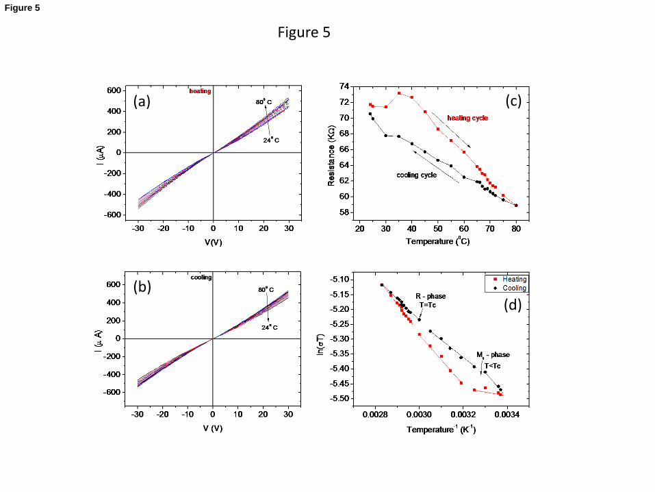
The current-voltage characteristics curves of the VO2 spot in film are presented in Fig. 5, the
curves in Fig. 5 (a) were for heating cycle from 24 0C to 80
0C and Fig. 5 (b) were for cooling
cycle from 80 0C back to 24
0C. These measurements show some shifts in the resistance of
the material as we change temperature from low to high which confirm the thermally
induced MIT nature of VO2 and this shows that Vanadium atoms override tungsten atoms in
forming metal oxide due to their high energy of formation of -7.03 eV/mol compared to
8.42 eV/mol for W [49].
The average resistance for each measurement were plotted against the temperatures and
the resulting picture is the hysteresis loop in Fig. 5 (c) with two distinct steps, the first at
high resistant insulating (monoclinic) phase and the other at low resistant metallic (metallic)
phase. Fig. 5 (d), the plot of Mott’s model that was discussed in section 2.2 of this report
shows similar steps trend for the product of conductivity and temperature versus the
inverse of temperature. Both heating and cooling cycle’s data were fitted linearly to obtain
the activation energy of hopping electrons in the material as Eq. (6) suggested. It was

found that the energies are 0.066 eV for heating and 0.054 eV for cooling. The heating
hopping value of 0.128 eV has been reported for VO2 nanowire [50].
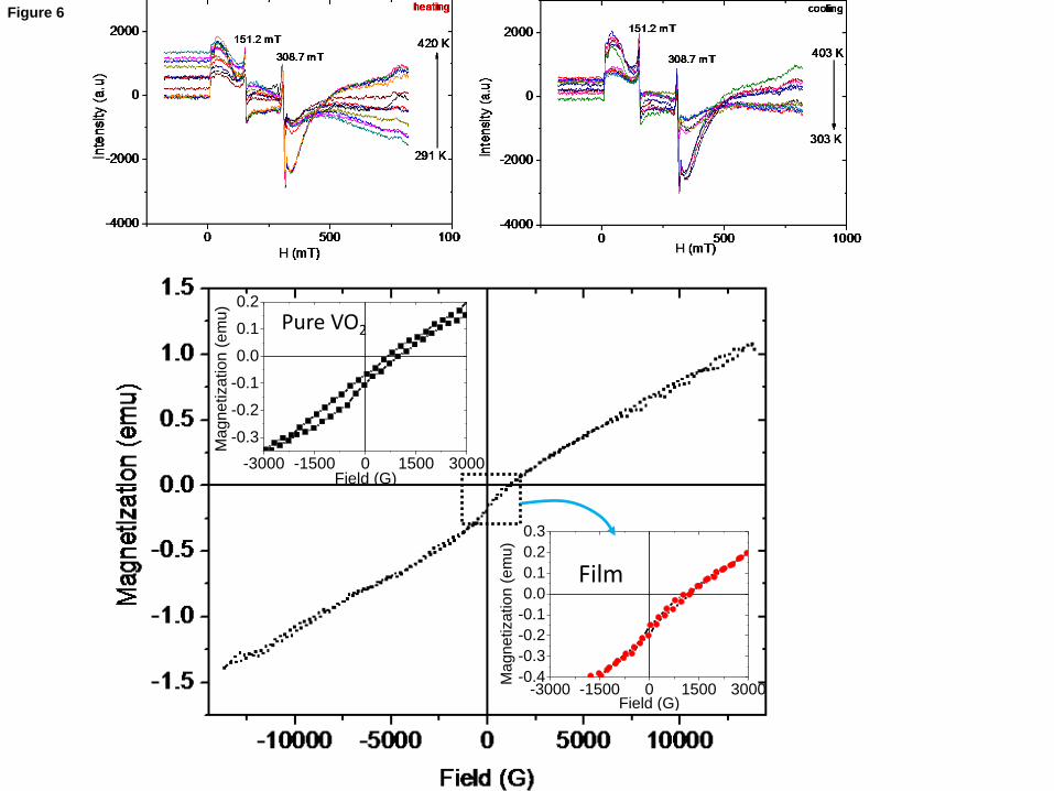
Magnetic property of the spot was investigated and Fig. 6 shows the ESR spectrum in Fig. 6
(a) for heating measurements from 291 K to 420 K, and 7 (b) for cooling measurements from
303 K to 403 K. Two distinct sharp peaks of materials were observed, one at a low field of
151.2 mT and the other at a high field of 308.7 mT. These spectra show some improvement
in intensity of the material as the temperature changes which indicates the
ordering/alignment of the electron spins in the material with respect to increase in
temperature and consequently the increase in magnetic moment.
Some authors on ESR have ascribed sharp ESR line-shapes to para-magnetism and broad ESR
line-shapes to ferro-magnetism [53]. This argument is based on the fact that ESR is in fact
sometimes referred to as EPR (electron paramagnetic resonance) and therefore sharp and
intense resonances are ascribed to para-magnetism. However other authors [54] on ESR
have explained sharp or broad as ferro or para respectively to the contrary; this difference
in opinions shows that the use of the nature of the ESR line-shapes to ferro or para
magnetism is not yet resolved in ESR or EPR. In order to ascertain the para or ferro
magnetism in this film, we have undertaken Vibrating Sample Magnetometry (VSM) in order
to obtain M vs H hysteresis curves. We have obtained M vs H hysteresis curves from a
commercial and pure VO2 samples.
Fig. 6 (c) displays the plot of magnetization, M, against the applied field, H, from the VSM
technique. This plot reveals that the film is composed of a paramagnetic phase and a small
ordered phase. The shift of the hysteresis loop away from the (0,0) point is a clear indication
of the multi-phase nature of the film which may present frozen magnetic moments of
varying orientations such that it takes a finite threshold applied field in order to bring all
these moments to a net zero magnetization. Above such a threshold (HT) field, the moments
align with the applied field and a finite amount of magnetization appears in the sample. The
shift in the M-H plots in Fig 6 (c-e) may be attributed to “exchange bias effect”[55] which is
observed in nano-scale materials.
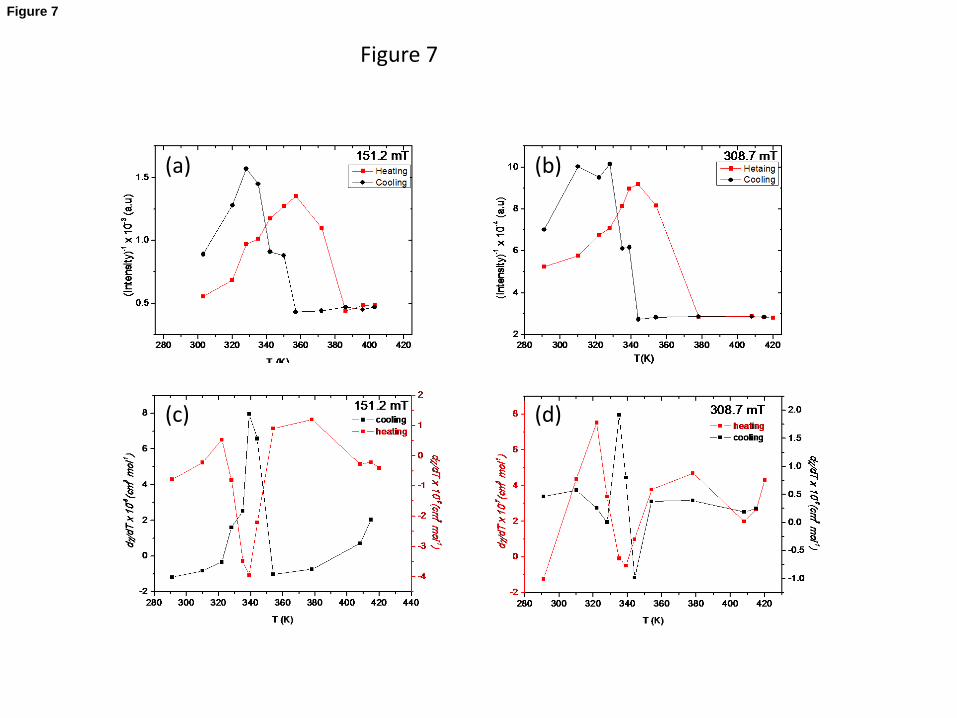
The plots of the inverse of intensity versus temperature were presented in Fig. 7. In Fig. 7 (a)
151.2 mT peaks was considered for both heating and cooling measurements with an
agreement around 338 K, and in Fig. 7 (b) 308.7 mT peaks was considered for both heating
and cooling measurements and also with an agreement around 336 K. Fig. 7 (c and d) shows
the derivative magnetic susceptibility of the ESR data that was calculated using Equation
(1) and the derivative of the results was considered for phase transition as explained in
section 2.2 of this report. Fig. 7 (c) shows the derivative magnetic susceptibility for heating
and cooling data produced by 151.2 mT field and Fig 7 (d) presents the derivative magnetic
susceptibility for heating and cooling data produced by 308.7 mT. Two distinct transitions of
339 K for heating and 338 K for cooling data for 151.2 mT field were obtained and similar
results were also obtained for 308.7 mT field i.e. 336 K for heating and 335 K for cooling
data, respectively.
Hysteresis width in the changes of the magnetic and susceptibility MIT is found to be 1K.
When compared to the hysteresis in the electrical conductivity MIT in Fig. 5 (c) of more than
30 K, one leads to the fact that magnetic properties, though linked to electronic properties,
display completely different hysteresis characteristics. The hysteresis loop width in most of
the properties reviewed above: conductivity, optical, phonon intensity, surface roughness
and surface plasmon resonance all display a widening hysteresis loop as the crystallite size
decreases.
5.0 Conclusion
In summary we have reported the magnetic property of heavily W-alloyed VO2 system; the
ESR method has proven that VO2 has a huge change in magnetic properties around its MIT.
Transition was found to occur around the MIT, 339 K for heating data and 338 K for cooling
data for 151.2 mT field peaks and similarly 336 K for heating data and 335 K for cooling data
308.7 mT field peaks. This MIT was confirmed with electrical measurement and the result
shows a shift in the resistance of the material from the insulating state to the metallic state.
Segregation of W and V atoms is observed as opposed to their diffusion. This could be due
to the high concentration of W. Finally, there is a hybridization of O 2p in favour of
vanadium atoms rather than tungsten atoms due to the high energy of formation of the
vanadium dioxide. Magnetic susceptibility as a function of temperature is presented here as
another means of tracking the VO2 metal-to-insulator transition temperature.
Acknowledgements
The authors acknowledge the financial support from the India-Brazil-South Africa trilateral
programme with a project number HGER24X and the CSIR National Centre for Nano-
Structured Materials project number HGER27S.
References
[1] M. Imada, A. Fujimori, Y. Tokura, Metal-insulator transitions, Rev. of Modern Phy 70, No.
4 1039-1263 (1998).
[2] N.F. Mott, Metal-insulator Transition, Rev. Modern Phys. 40 (4) (1968) 677.
[3] D. Adler, Mechanisms for Metal-Nonmetal Transitions in Transitions-Metal Oxides and
Surfides, Rev. Modern Phys. 40 (4) (1968) 714-736.
[4] F.J. Morin, Oxides which show a metal-insulator-transition at Neel temperature, Phys.
Rev. Lett. 3, (1959) 34.
[5] P. Kiria, G. Hyettb, R. Binions, Solid state thermochromic materials, Adv. Mat. Lett. 1(2),
86-105 (2010)
[6] J.B. Goodenough, The two components of Crystallographic transition in VO2, J. Solid
State Chem. 3, 490-500 (1971).
[7] S. Shin, S. Suga, M. Tanuguchi, M. Fijisawa, H. Kansaki, A. Fujimori, H. Damon, Y. Ueda, K.
Kosuge, S. Kachi, Vacuum-ultraviolet reflectance and photoemission study of the metal-
insulator phase transitions in VO2, V6O13, and V2O3, Phys. Rev. B 41, 4993-5009 (1990).
[8] J.M. Reyes, J.R. Marko and M.Sayer, Hysteresis in the Semiconductor-Metal Transition of
Cr-doped VO2, Sol. St. Comm, Vol. 13 1953-1957 (1973)
[9] D. Paquet, P. Leroux-Hugon, Electron correlations and electron-lattice interactions in the
metal-insulator, ferroelastic transition in VO2: A thermodynamical study, Phys. Rev. B22,
5284-5301 (1980).
[10] N.F. Mott, R. Peierls, Discussion of the paper by de Boer and Verwey Proc. Phys. Soc.
London, Ser. A. 49, 72 (1937).

[11] A. I. Buzdin, L N. Bulaevskii, P. N. Lebedev, Spin-Peierls transition in quasi-one-
dimensional crystals, Physics Institute, Academy of Sciences of the USSR, Moscow Usp Fiz
Nauk, 131, 495-510 (July 1980).
[12] R. Lopez, L.A. Boatner, T.E. Haynes, R.F. Haglund, Jr. Feldman, L.C. Feldman, Enhanced
hysteresis in the semiconductor-to-metal phase transition of VO2 precipitates formed in SiO2
by ion implantation, Phy Letters 79 (2001) 19.
[13] X.J. Wang, H.D. Li, Y.J. Fei, X. Wang, Y.Y. Xiong, Y.X. Nei, K.A. Feng, XRD and Raman
study of vanadium oxide thin film deposits on fused silica substrates by RF Magnetron
Sputtering, Applied surface science 177 ( 2001) 8-14.
[14] M-H. Lee, J.S. Cho, Better Thermochromic glazing of windows with ant-reflection
coating, Thin Solid Film 365 5-6 (2000).
[15] L. Alberto, L. de Almeida, G. S. Deep, A. Mercus, N. Lima, H. Neff and R. S. Freire, A
Hysteresis Model for Vanadium Oxide Thermal Radiation Sensor, IEEE Instrumentation
Measurement Technology Conference 2000.
[16] E. Strelcov, Y. Lilach, A. Kolmakov, Gas Sensor Based on Metal-Insulator Transition in
VO2 Nanowire Thermistor, Nano Letters 2009, Vol. 9, No. 6, 2322-23269
[17] A. Pergrament, G. Stefanovich, O. Berezina, D. Kirienko, Electrical conductivity of
tungsten doped vanadium dioxide obtained by the sol-gel technique, Thin Solid Films 572-
576 (2013)
[18] Y. Gao, H. Luo, Z. Zhang, L. Kang, Z. Chen, J. Du, M. Kanehira, C. Cao, Nanoceramic VO2
thermochromic smart glass: A review on progress in solution processing, Nano Energy
(2012) 1, 221-246.

[19] W. Burkhardt, T. Christmann, B.K. Meyer, W. Niessner, D. Schalch, A. Scharmann , W-
and F-doped VO2 films studied by photoelectron spectrometry, Thin Sol. Films. 345 (1999)
229-235.
[20] O. Y. Berezina, A. A. Velichko, L.A. Lugovskaya, A.L. Pergament, G.B. Stefanovich, D.V.
Artyukhin, A. N. Strelko, Properties of Tungsten-Doped Vanadium Oxide Films, Tech. Phys.
Lett. (2007) Vol. 33, No. 7, pp. 552-555.
[21] R. Binions, G. Hyett, C. Piccirillo, I. P. Parkin, Doped and Undoped vanadium dioxide thin
films prepared by atmospheric pressure chemical vapour deposition from vanadyl
acetylacetonate and tungsten hexachloride: the effects of thickness and crystallographic
orientation on thermocromic properties, J. Mat. Chem. 17, 4652-4660 (2007)
[22] V. Eyert, The metal-insulator transitions of VO2: A band theoretical approach Ann. Phys.
(Leipzig) 11, 1-61 (2002) 9.
[23] M. Pan, J. Liu, H-M. Zhong, S-W. Wang, Z-F. Li, X-S. Chen, Wei Lu, Raman study of the
phase transition in VO2 thin films J. of Cry. Growth 268 (2004) 178–183
[24] C. Marini, E. Arcangeletti, D. Di Castro, L. Baldassare, A. Perucchi, S. Lupi, L. Malavasi, L
Boeri, E. Pomjakushina, K. Conder, P. Postorino, Optical properties of V1−xCrxO2
compounds under high pressure, Phy Rev. B 77, 235111-9, 2008
[25] B. W. Mwakikunga, E. Sideras-Haddad, M. Maaza, First synthesis of vanadium dioxide
by ultrasonic nebula-spray pyrolysis, Optical Materials 29 (2007) 481–487
[26] S.-Y. Li, G. A. Niklasson, and C. G. Granqvist, Nanothermochromics: Calculations for VO2
nanoparticles in dielectric hosts show much improved luminous transmittance and solar
energy transmittance modulation, J. Appl. Phys. 108, 063525 (2010).
[27] R. Lopez, R. F. Haglund, Jr., L. C. Feldman, L. A. Boatner, T. E. Hayness, Optical
nonlinearities in VO2 nanoparticles and thin films, App. Phy. Lett 85, (2004).
[28] S. Lysenko, A. Rua, F. Fernandez, H. Liu, Vanadium dioxide based plasmonic modulators,
J. Appl. Phys. 105, 043502 (2009)
[29] J. Cao, W. Fan, J-Q. Wu, Strain and temperature dependence of the insulating phases of
VO2 near the metal-insulator transition, Phy. Rev. B 85, 020101(R) (2012)
[30] Z. Lu, C-G.Lia,Y. Yin, Synthesis and thermochromic properties of vanadium dioxide
colloidal Particles, J. Mater. Chem., 2011, 21, 14776-14782
[31] E .U. Donev, J. I. Ziegler, R. F Haglund Jr., L. C. Feldman, Size effects in the structural
phase transition of VO2 nanoparticles studied by surface-enhanced Raman scattering, J. Opt.
A: Pure Appl. Opt. 11(2009) 125002 (8pp).
[32] A. C. Jones, S. Berweger, J. Wei, D. Cobden, M. B. Raschke, Nano-optical investigations
of the metal-insulator phase behaviour of individual VO(2) microcrystals, Nano Lett. 2010,
10, 1574–1581.
[33] M. Maaza, O. Nemraoui, C. Sella, A. C. Beye, B. Baruch-Barak, Thermal induced
tenability of surface plasmon resonance in Au-VO2 nano-photonics, Optics Comm. 254
(2005) 188-195.
[34] J. Khalifeh, Magnetic structure of vanadium overlayers on semi-infinite substrate, J.
Mag. Mat. 168 (1997) 25-30.
[35] H. Akoh and A. Tasaki, Appearance of Magnetic moments in Hyperfine particles of
Vanadium Metal, J. Phys. Soc. Jap. 42, 791 (1977).

[36] A. M. Bakir, B. A. Hamad,J. M. Khalifeh, Surface and interface magnetism of V/W
systems, phys. stat. sol. (b) 242, No. 12, 2522–2529 (2005)
[37] I. Bertini, C. Luchinat, G. Patirigi, Magnetic susceptibility in paramagnetic NMR, Prog. in
N.M.R, Spec. 40 (2002) 247-273.
[38] R. Boca, Mean and differential magnetic susceptibilities in metal complexes, Coord
Chem. Rev. 173 (1998) 167–283.
[39] M. D. Vannette, Dynamic magnetic susceptibility of systems with long-range magnetic
order, Graduate Theses and Dissertations, Iowa State University,
http://lib.dr.iastate.edu/etd (2009).
[40] N.F. Mott, Conduction in glasses containing transition metal ions, J. Non-Cryst. Solids 1
(1968) 1-17
[41] S. A. Corr, M. Grossman, Y. Shi, K. R. Heier, G. D. Stucky, R.SeshadriJ, VO2(B) nanorods:
solvothermal preparation, electrical properties, and conversion to rutile VO2 and V2O3,
Mater. Chem., 2009, 19, 4362–4367
[42] S. Pavasupree, Y. Suzuki, A. Kitiyanan, S. Pivsa-Art, S. Yoshikawa, Synthesis and
Characterization of vanadium oxides nanorods, J. Solid Sat. Chem. 178 (2005) 2152–2158
[43] B.W. Mwakikunga, E.Sideras-Haddad, C. Arendse , M. J. Witcomb, A. Forbes, Raman
spectroscopy of WO3 nano-wires and thermo-chromism study of VO2 belts produced by
ultrasonic spray and laser pyrolysis techniques, J. Nanosc. & Nanotech. Vol. 8, 1-9, 2008
[44] C. Julien, G. A. Nazri, and O. Bergstrom, Raman Scattering Studies of Microcrystalline
V6O13, Phys. Stat. Solidi B 201, 319-326 (1997)

[45] G.I. Petrov, V.V. Yakovlev, J. Squier, Raman microscopy analysis of phase transformation
mechanisms in vanadium dioxide Appl. Phys. Lett. 81 (6) (2002) 1023-1025.
[46] E. Cazzanelli, C. Vinegoni,- G. Mariotto,- A. Kuzmin,à and J. Puransà, Low-Temperature
Polymorphism in Tungsten Trioxide Powders and Its Dependence on Mechanical
Treatments, J. of Sol. St. Chem. 143, 24-32 (1999).
[47] F. Beteille, J. Livage, Optical Switching in VO2 Thin films, J. of Sol-Gel Sc. and Tech. 13,
915–921 (1998)
[48] C. S. Blackman, C. Piccirillo, R. Binions, Ivan P. Parkin, Atmospheric pressure chemical
vapour deposition of thermochromic tungsten doped vanadium dioxide thin films for use in
architectural glazing, Thin Solid Films 517 (2009) 4565–4570.
[49] B W Mwakikunga, A. E. Mudau, N. Brink, C.J. Willers, Flame temperature trends in
reacting vanadium and tungsten ethoxide fluid sprays during CO2-laser pyrolysis, Appl. Phys
B 105, 451-462 (2011).
[50] X. Wu, Y.Tao, L. Dong, Z. Wang, Z. Hu, Preparation of VO2 nanowires and their electric
characterization, Mat. Res. Bullet. 40 (2005) 315–321.
[51] F. Theobald, R. Cabala, J. Bernard, Test on the structure of VO2 (B), J. Solid State Chem.,
17 (1976) 431
[52] Y. Oka, T. Yao, N. Yamamoto, Y. Ueda, A. Hayashi, Phase transition and V4+
-V4+
pairing in
VO 2 (B), J. Solid State Chem. 105 (1993) 271
[53] S. S. Nkosi, H. M. Gavi, D. E. Motaung, J. Keartland, E. Sideras-Haddad, A. Forbes, B . W.
Mwakikunga, Ferromagnetic resonance characterization of nano-FePt by electron spin
resonance, J. Spectrosc. 2013 (2013) art ID 272704, 6 pages
[54] A. Martins, S. C. Trippe, A. D. Santos, F. Pelegrini, Spin-wave resonance and magnetic
anisotropy in FePt thin films, J. Magnetism Magnetic Mater. 302 (2007) 120-125
[55] J Nogués, J Sort, V. Langlais, V. Skumryev, S. Surinack, J. S. Munoz, M. D. Barό, Exchange
bias in nanostructures, Phys. Rep. 422 (2005) 65-117
Figure Captions
Fig. 1 The electronic energy band diagram of the VO2 system as proposed by Goodenough
[6].
Fig. 2 Variation of VO2 properties with temperature close to MIT: (a) Resistance and
Conductance, (b) Transmittance and Reflectance, (c) Roughness (d) Scattering , (e) Raman
relative intensity of 618 cm-1
phonon frequency and (f) Surface Plasmon resonance
wavelength.
Fig. 3 (a) X-Ray diffraction pattern of the mixtures of WO3 and VOx film (b) Room
temperature Raman spectrum of the same film (c) XPS spectrum of the film (d) Higher
resolution XPS of the WOx regions (e) Higher resolution XPS of the VOx regions.
Fig. 4 (a) SEM mapping of VO2 and W over layered system, (b) corresponding EDS of Fig.
5(a), (c) TEM image of VO2 localized site, (d) corresponding EDS spectrum of Fig. 5 (c), (e) W
localized sit and the spot showing VO2 and W hybridization ( f) EDS and SAED pattern of the
VO2 and W hybridization spot.
Fig. 5 I-V characteristic curves of the VO2 localized site (a) Heating cycle measurements from
room to above transition and (b) Cooling cycle measurements from transition down to room
temperature. (c) Temperature dependence Resistance measurements of the VO2 site (a)
from room to above transition and (d) ln against 1/T of VO2 site for heating and
cooling cycle measurements.
Fig. 6 Electron Spin Resonance spectra of the VO2 film (a) spectra for heating cycle
measurement (b) spectra for cooling cycle measurement and (c) M vs H curve for the film

obtained from Vibrating Sample Magnetometry (VSM). (d) (inset) M vs H curve for pure VO2
samples (e) (inset) M vs H curve for present thin film.
Fig. 7 Thermochromic hysteresis measure as inverse of ESR intensity against temperature
for (a) 151.2 mT and (b) 308.7 mT peaks. Derivative of the magnetic susceptibility for (c)
151.2 mT heating data and 151.2 mT cooling data and (d) 308.7 mT heating data and 308.7
mT cooling data. In all a transition at 340 K is evident.
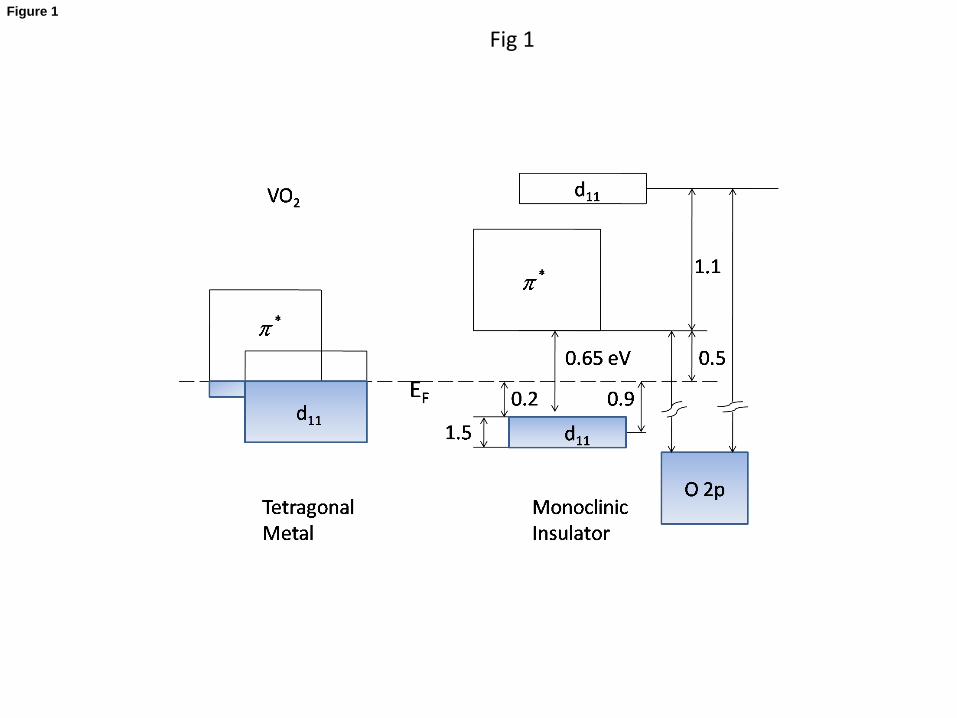
Fig 1
Figure 1

104
102
10-2
10-3
10-4
10-5
103
101 Res
ista
nce
(o
hm
s)
Co
nd
uct
an
ce, S
Tra
nsm
itta
nce
(%
)
Ref
lect
an
ce (
%)
20
40
60
80
100
20
40
60
80
100
280 360 T (K)
280 360 T (K)
20
40
60
80
100
20
40
60
80
100
280 360 T (K)
Ro
ug
hn
ess
(nm
)
20
40
60
80
100
20
40
60
80
100
280 360 T (K)
Sca
tter
ing
Inte
nsi
ty (
a.u
)
T (K)
Rel
ati
ve In
ten
sity
(a
.u)
0.2
0.4
0.6
0.8
1.0
0.2
0.4
0.6
0.8
1.0
280 360 600
610
620
630
640
600
610
620
630
640
280 360 T (K)
Surf
ace
Pla
smo
n R
eso
na
nce
W
ave
len
gth
(a
.u)
(a) (b) (c)
(d) (e) (f)
Fig 2 Figure 2
Figure 3
(a) (b)
(c)
(d)
(e)
Figure 3

Fig 4
O V
W
C
V
V W W W
Ca K Ca Na
W V O Ca S Na K
Figure 4
(a)
(b)
(c)
(d)
Figure 5
Figure 5
-3000 -1500 0 1500 3000
-0.3
-0.2
-0.1
0.0
0.1
0.2
Magnetization (
em
u)
Field (G)
-3000 -1500 0 1500 3000-0.4
-0.3
-0.2
-0.1
0.0
0.1
0.2
0.3
Ma
gn
etiza
tio
n (
em
u)
Field (G)
Pure VO2
Film
Figure 6
(a) (b)
(c) (d)
Figure 7
Figure 7