emul196–pc™ - welcome to ice technology the world's ... · universal serial bus (usb) ......
TRANSCRIPT
EMUL196–PC™User Guide
Edition 1, June 6, 2001
© 2001 All rights reserved worldwide.
EMUL196–PC User GuideEMUL196–PC User GuideEMUL196–PC User GuideEMUL196–PC User Guide
Edition 1, June 6, 2001 © iiii
Contents
About This Guide x
Downloading EMUL196–PC Product Documentation x
Overview of the EMUL196–PC Emulator System 1
High-Speed Parallel (HSP) Box 2
Universal Serial Bus (USB) Box 2
PC Plug-In/Industry Standard Architecture (ISA) 3
Low-Cost Industry Standard Architecture (LC–ISA) 3
User Interface 3
Quick Start for Installing Your Emulator System 4
Quick Start for Installing the Hardware 5
Installing and Configuring the Seehau Software 7
Configuring the Seehau Software 7
Running the Configuration Software 8
Purchasers of Emulator and Trace Boards 10
Configuring Address Settings With Windows Operating Systems 11
Configuring Address Settings for the Emulator and Optional Trace Board 11
Information about Windows NT Installation 11
Known Device Driver Conflicts 11
Configuring Address Settings with Windows 95/98 12
Configuring Address Settings with Windows NT 13
Configuring Address Settings with Windows 2000 16
iiiiiiii EMUL196–PC User Guide
Installing and Configuring the Emulator Board 21
Installing the Emulator Board 22
Emulator Installation Instructions 23
Setting the I/O Address Jumpers: J2 23
Typical PC I/O Addresses 23
Addressing Examples 24
Header JP1 24
Header J4 24
Installing the Emulator Board into the ISA Slot 25
Shadow RAM 25
Quick-Save Settings 266
Installing and Configuring the Trace Board 27
Hardware Description 27
Installation Instructions 27
I/O Address 27
External Inputs and Controls 28
Tracing Overview 30
Trace Modes 30
Trace Window 31
Trace Menu 32
Trace Configuration 33
Trace Setup Tab 33
Trigger / Filter ConfigurationTabs 35
Entering Addresses and Data 36
Opcode Trigger Mode 36
Data Trigger Mode 37
Data to Trigger On 37
Other Controls for Trace Configuration 38
EMUL196–PC User GuideEMUL196–PC User GuideEMUL196–PC User GuideEMUL196–PC User Guide
Edition 1, June 6, 2001 © iiiiiiiiiiii
Accessories and Adapters 39
Type of Adapters 39
Verifying the Orientation of Your Adapter 39
Creating a Shortcut to PicView 40
Installing and Configuring the Pod Board 41
Overview 41
Features Common to All Pod Boards 41
Stack Pointer 41
Indicator Lights 42
How to Simultaneously Stop Code Execution on Two Emulators 42
Trace Input Pins 42
Resource Selection 42
Power 43
XTAL 43
Microcontroller 43
Clip-Over Adapter 44
Summary of Hardware Configuration 44
Memory Map Configuration Requirements 44
Enough Emulator Memory? 45
Internal Addressing or Single-Chip Mode 45
Replacing Ports: POD196–KR/NT and CA/CB 45
Port Replacement Unit (PRU) 46
Program Performance Analyzer (PPA) 46
Code Coverage 46
iviviviv EMUL196–PC User Guide
Pod Boards 47
POD196–KC / KD 47
Overview 47
Dimensions 47
Emulation Memory 48
Wait States 48
Headers and Jumpers 48
Procedure to Test 53
Memory Mapping 53
Hardware Breakpoint Setup 54
Helpful Hints for Compiling 54
Download Procedure 55
POD196–KR / NT 56
Overview 56
Dimensions 56
NMI Pin (KR/NT only) 57
PRU 57
Emulation Memory 57
Headers and Jumpers 57
KR/NT Ready Functionality 61
POD196–NP / NU 64
Overview 64
Dimensions 64
Emulation Memory 65
Wait States 65
Headers and Jumpers 66
Symbols in the Trace Window 71
Mapping Memory Using Chip Selects 72
Port Replacement Unit 74
Overview 74
When to Use a Port Replacement Unit 74
Installing the PRU 75
PRU Headers and Jumpers 75
PRU Special Function Registers 76
Design Limitations and Silicon Bugs—PRU 78
PRU Header JP2—Accessing P3, P4 and P5 78
EMUL196–PC User GuideEMUL196–PC User GuideEMUL196–PC User GuideEMUL196–PC User Guide
Edition 1, June 6, 2001 © vvvv
Starting the Emulator and Seehau Software 83
Hardware Connection 83
Starting Seehau 84
Time Program Example 85
Example Program 85
Watching Data in Real-Time with Shadow RAM 86
Trace Memory Example 89
Overview 89
Running the Example 89
Saving the Configuration 91
Shutting Down Seehau 93
Steps to Shut Down Seehau 93
Important Software and Hardware Notes 94
Appendix A. Troubleshooting 95
Overview 95
Stack Pointer 96
HSP/USB Box 97
Debugging the Parallel Port 99
Windows NT Users 99
Windows 9x Users 99
Windows 2000 Users 99
ISA 104
vivivivi EMUL196–PC User Guide
If the Emulator Does Not Start When Connected tothe Target System 105
Board I/O Addresses 105
Emulator Configuration Utility Screen 106
PWR and XTAL Jumpers 106
I/O on Address Pins 107
Chip Configuration Bytes (CCBs) 107
Enough Memory 107
The Stack Pointer 107
Interrupt Vectors 108
Nonmaskable Interrupt (NMI) Pin (KR/NT only) 108
Buswidth (CA/CB only) 108
Single-Chip Mode 109
Sample User Program 109
Appendix B. ISO–160 111
PLCC–52–ISO 111
EMUL196/ISO-160 111
SAMTEC/SSQ–117–03–GD 113
Appendix C. Compilers 115
Overview 115
Tasking 115
Compiler Notes 115
Assembler Notes 115
IAR 116
Appendix D. Emulator / Trace Address Examples 117
EMUL196–PC User GuideEMUL196–PC User GuideEMUL196–PC User GuideEMUL196–PC User Guide
Edition 1, June 6, 2001 © vii viiviivii
Appendix E. Discontinued Pod Boards 121
POD196–CA / CB 121
Overview 121
Dimensions 122
Emulation Memory 122
INST 122
Port Replacement Unit (PRU) 122
Nonmaskable Interrupt (NMI) Pin 123
Headers and Jumpers 123
87C196CB Bondout Errata 126
POD196–EA 134
Overview 134
Dimensions 134
Emulation Memory 135
Addressing RAM 135
8-Bit Mode and BHE Mode 136
Headers and Jumpers 136
Symbols in the Trace Window 140
Memory Mapping 141
Port Replacement Unit (PRU) 141
POD–196LC–KR/NT 142
Overview 142
Dimensions 143
PRU 143
Emulation Memory 143
Headers and Jumpers 143
Glossary 147
Index
Sales Offices, Representatives and Distributors

viiiviiiviiiviii EMUL196–PC User Guide
Product Notes
European CE RequirementsNohau has included the following information in order to comply with European CE requirements.
User ResponsibilityThe in-circuit debugger application, as well as all other unprotected circuits need special mitiga-tion to ensure Electromagnetic Compatibility (EMC).
The user has the responsibility to take required measures in the environment to prevent otheractivities from disturbances from the debugger application according to the user and installationmanual.
If the debugger is used in a harsh environment (field service applications for example), it is theuser’s responsibility to control that other activities cannot be disturbed in such a way that theremight be risk for personal hazard/injuries.
Special Measures for Electromagnetic Emission RequirementsTo reduce the disturbances to meet conducted emission requirements it is necessary to place aground plane on the table under the pod cable and the connected processor board. The groundplane shall have a low impedance ground connection to the host computer frame. The insulationsheet between the ground plane and circuit boards shall not exceed 1mm of thickness.
Warnings
To avoid damage to the pod or to your target, do not connect the pod to your target whenthe pod or target power is on.
When powering up, always power up the emulator first followed by the target system.When powering down, power down the target system first followed by the emulator.Failing to do so can cause damage to your target and/or emulator.
Do not apply power to your system unless you are sure the target adapter is correctlyoriented. Failing to do so can cause damage to your target and/or emulator.
When using the pod with a target, disable all pod resources that are duplicated on the tar-get. Failure to disable the pod’s resources can damage the pod or the target or both. Thisincludes the MCU, the serial port, RAM, crystal, and, particularly, the power supply. Ifusing the clip to attach to the target, remove the MCU from the pod.
When installing a controller into a pod, never press on the chip body. Press only on thecarrier or cover. Pressing on the chip can bend pins and cause short circuits.
EMUL196–PC User GuideEMUL196–PC User GuideEMUL196–PC User GuideEMUL196–PC User Guide
Edition 1, June 6, 2001 © ixixixix
Minimum System Requirements
CAUTION
Like all Windows applications, the Seehau software requires a minimum amount of free operat-ing system resources. The recommended amount is at least 40%. (This is only a guideline. Thispercentage might vary depending on your PC.) If your resources are dangerously low, Seehaumight become slow, unresponsive or even unstable. If you encounter any of these conditions,check your free resources. If they are below 40%, reboot and limit the number of concurrentlyrunning applications. If you are unable to free at least 40% of your operating system resources,contact your system administrator or Nohau Technical Support at [email protected].
The following are minimum system requirements:
• Pentium 200 (Pentium II or faster is recommended)
• Single-Processor System
• Windows 95, 98, NT, 2000, or 2000 ME
• Random Access Memory (RAM)– For Windows 95/98: 64 MB– For Windows NT/2000/2000ME: 128 MB
• Two ISA slots in your PC if the optional trace board is purchased, otherwise purchase theHSP or USB box.
xxxx EMUL196–PC User Guide
About This Guide
The EMUL196–PC User Guide describes how to use the EMUL196–PC emulation system withthe Seehau graphical user interface. This guide is intended for both novice and advanced users.
The EMUL196–PC is a PC-based emulator for the Intel 80C196 family of microprocessors.This guide helps you to get started with the basics of setting up, configuring, and running theSeehau software and the emulator. If you have any questions contact Nohau Technical Supportat [email protected] or refer to the Sales Offices, Representatives and Distributors list at theend of this guide.
Online context sensitive Help is also available from the Seehau software by pressing the F1 or theHelp keys, depending on the type of keyboard you have.
The EMUL196–PC User Guide introduces the following tasks:
• Installing and Configuring the Seehau Software
• Installing and Configuring the Emulator
• Installing and Configuring Trace Boards
• Types of Adapters
• Installing and Configuring Pods
• Starting the Emulator and Seehau Software
• Time Program Examples
• Trace Memory Example
• Macro Example
• Shutting Down Seehau Software
• Troubleshooting
• Hex Pin Addressing
• Glossary
Downloading EMUL196–PC Product Documentation
To download an electronic version of this guide, do the following:
1. Open Nohau’s home page at www.nohau.com.
2. Click Publications.
3. Click Nohau Manuals.
4. Scroll down to EMUL196–PC. Then select EMUL196–PC to download a PDF versionof this guide.
EMUL196–PC User GuideEMUL196–PC User GuideEMUL196–PC User GuideEMUL196–PC User Guide
Edition 1, June 6, 2001 © 1111
Overview of the EMUL196–PCEmulator System
The basic hardware for the EMUL196–PC emulator system includes the following:
• Emulator board—plugs into an ISA slot inside the PC, HSP or USB box.
• Standard or Data trace board (optional)—plugs into an ISA slot inside the PC, HSP or USBbox and connects to the emulator board through two short ribbon cables.
• Pod board—the device that allows you to emulate the device under development.
• Five-foot twisted-pair ribbon cable—connects the emulator and pod.
• Combination 25-pin to 50-pin cable (part number CBL-A-LC25/50) for the LC–ISA only.
• Target adapter—allows you to connect the pod board to your target system.
To connect to your target system, the pod board usually requires an adapter. To determine theadapter board that your pod requires, check the price list, your representative or Nohau TechnicalSupport at [email protected].
The EMUL196–PC emulator consists of an emulator and a pod board. The pod board typicallyrequires an adapter to connect to your target system. An optional trace board can be added to allsystems except for the low-cost systems (LC–ISA) for advanced tracing capabilities. Four systemconfigurations are available to suit your needs:
• High-Speed Parallel (HSP) Box connects to the parallel printer port. See the following“High-Speed Parallel (HSP) Box” section.
• Universal Serial Bus (USB) Box. See the following “Universal Serial Bus (USB) Box”section.
• PC Plug-In/Industry Standard Architecture (ISA). See the following “PC Plug-In/IndustryStandard Architecture (ISA)” section.
• Low-Cost Industry Standard Architecture (LC–ISA). See the following “Low-Cost IndustryStandard Architecture (LC–ISA)” section.
You can configure the emulator hardware to your requirements with various jumpers. For detailson configuring your emulator board, refer to Chapter 3, “Installing and Configuring the EmulatorBoard.” For details about the optional trace board, refer to Chapter 5, “Installing and Configuringthe Trace Board,” or go to Seehau Help in the software.
Chapter 1. Overview of the EMUL196–PC Emulator SystemChapter 1. Overview of the EMUL196–PC Emulator SystemChapter 1. Overview of the EMUL196–PC Emulator SystemChapter 1. Overview of the EMUL196–PC Emulator System
2222 EMUL196–PC User Guide
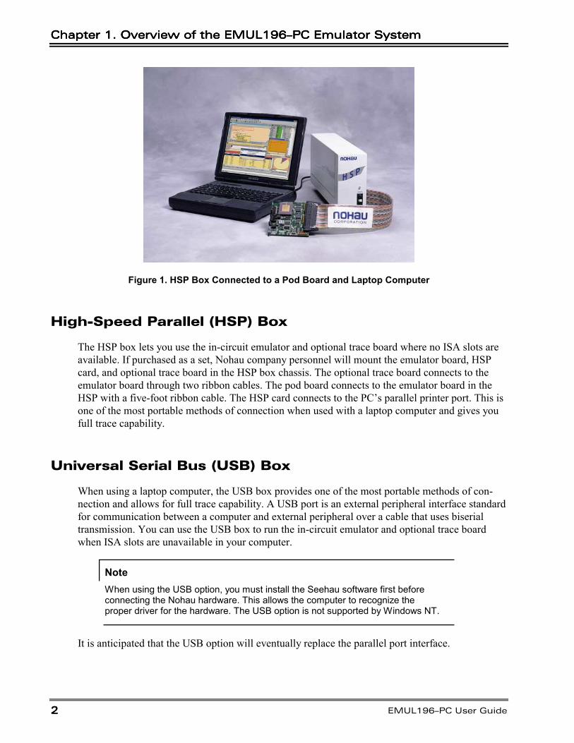
Figure 1. HSP Box Connected to a Pod Board and Laptop Computer
High-Speed Parallel (HSP) Box
The HSP box lets you use the in-circuit emulator and optional trace board where no ISA slots areavailable. If purchased as a set, Nohau company personnel will mount the emulator board, HSPcard, and optional trace board in the HSP box chassis. The optional trace board connects to theemulator board through two ribbon cables. The pod board connects to the emulator board in theHSP with a five-foot ribbon cable. The HSP card connects to the PC’s parallel printer port. This isone of the most portable methods of connection when used with a laptop computer and gives youfull trace capability.
Universal Serial Bus (USB) Box
When using a laptop computer, the USB box provides one of the most portable methods of con-nection and allows for full trace capability. A USB port is an external peripheral interface standardfor communication between a computer and external peripheral over a cable that uses biserialtransmission. You can use the USB box to run the in-circuit emulator and optional trace boardwhen ISA slots are unavailable in your computer.
NoteWhen using the USB option, you must install the Seehau software first beforeconnecting the Nohau hardware. This allows the computer to recognize theproper driver for the hardware. The USB option is not supported by Windows NT.
It is anticipated that the USB option will eventually replace the parallel port interface.

EMUL196–PC User GuideEMUL196–PC User GuideEMUL196–PC User GuideEMUL196–PC User Guide
Edition 1, June 6, 2001 © 3333
PC Plug-In/Industry Standard Architecture (ISA)
The emulator ISA board is plugged into an ISA slot in your PC, USB or HSP and is connectedwith a five-foot cable to a device-dependent pod board. The optional trace board can also beplugged into the PC, HSP or USB box and is connected to the emulator board through two shortribbon cables.
NoteIf the optional trace board were purchased for PC installation, you would need toensure that your computer motherboard has at least two open ISA slots or you willneed to purchase the HSP or USB box.
Low-Cost Industry Standard Architecture (LC–ISA)
The EMUL/LC–ISA board is an 8-bit PC card that fits into any ISA slot in your PC. This boardmust be connected to a pod board to operate. Low cost emulators do not have Shadow RAM, orprovision for a real-time trace (or the ability to add a trace board). The maximum frequency is setby the frequency limit on the pod board. The connection for the board to pod is through a 25-pinconnector from the board to a 50-pin connector to the pod (part number CBL–A–LC25/50).
User Interface
The emulator is configured and operated by the Seehau user interface. Seehau is a high-levellanguage user interface that allows you to perform the following tasks:
• Load, run, single-step and stop programs based on C or Assembly code.
• Set triggers and view trace (with optional trace board).
• Modify and view memory contents including Special Function Registers (SFRs).
• Set software and hardware breakpoints.
• Analyze code with Program Performance Analysis (PPA).
Chapter 1. Overview of the EMUL196–PC Emulator SystemChapter 1. Overview of the EMUL196–PC Emulator SystemChapter 1. Overview of the EMUL196–PC Emulator SystemChapter 1. Overview of the EMUL196–PC Emulator System
4444 EMUL196–PC User Guide
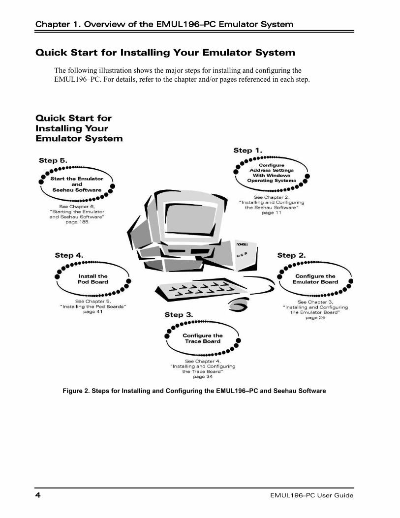
Quick Start for Installing Your Emulator System
The following illustration shows the major steps for installing and configuring theEMUL196–PC. For details, refer to the chapter and/or pages referenced in each step.
Figure 2. Steps for Installing and Configuring the EMUL196–PC and Seehau Software
EMUL196–PC User GuideEMUL196–PC User GuideEMUL196–PC User GuideEMUL196–PC User Guide
Edition 1, June 6, 2001 © 5555
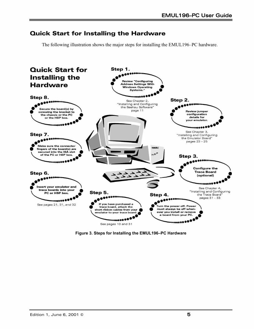
Quick Start for Installing the Hardware
The following illustration shows the major steps for installing the EMUL196–PC hardware.
Figure 3. Steps for Installing the EMUL196–PC Hardware
Chapter 1. Overview of the EMUL196–PC Emulator SystemChapter 1. Overview of the EMUL196–PC Emulator SystemChapter 1. Overview of the EMUL196–PC Emulator SystemChapter 1. Overview of the EMUL196–PC Emulator System
6666 EMUL196–PC User Guide
EMUL196–PC User GuideEMUL196–PC User GuideEMUL196–PC User GuideEMUL196–PC User Guide
Edition 1, June 6, 2001 © 7777
Installing and Configuring theSeehau Software
To install the Seehau software, do the following:
1. Locate your Seehau CD and insert the CD into your CD ROM drive. The installation processwill start automatically.
2. Follow the instructions that appear on your screen.
NoteIf the installation does not start automatically, you probably have your WindowsAutorun feature disabled. You will then need to use Windows Explorer and navigateto the CD root directory or right-click on the drive where the CD is located. If younavigate to the root directory find Autorun.exe and double-click on it. If youright-click on the drive where the CD is located, select AutoPlay to start theinstall process.
Configuring the Seehau Software
When first started, Seehau loads a configuration file called Startup.bas This file is created by theSeehau Configuration Program, which stores Startup.bas in the following directory:C:\Nohau\Seehau196\Macro
The Seehau software automatically starts Seehau Config if it does not find the startup file.
You do not need to have the emulator connected to the PC to run the Seehau Configuration Pro-gram. However, for the Seehau regular executable to operate, the emulator must be connected withthe jumpers set correctly.
Get familiar with the emulator in stand-alone mode (not connected to a target system) or the demomode before connecting to a target hardware system. The added complications of the target hard-ware might cause you problems at this time. Once you have gained some skills at operating theemulator, then connect to your target. To operate in Demo mode select Start/Programs/Seehau196/Demo.
Chapter 2. Installing and Configuring the Seehau SoftwareChapter 2. Installing and Configuring the Seehau SoftwareChapter 2. Installing and Configuring the Seehau SoftwareChapter 2. Installing and Configuring the Seehau Software
8888 EMUL196–PC User Guide
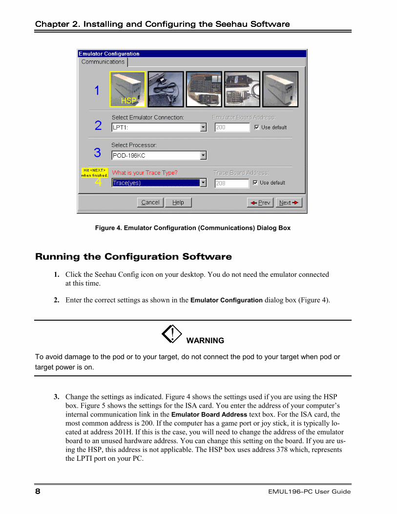
Figure 4. Emulator Configuration (Communications) Dialog Box
Running the Configuration Software
1. Click the Seehau Config icon on your desktop. You do not need the emulator connectedat this time.
2. Enter the correct settings as shown in the Emulator Configuration dialog box (Figure 4).
WARNING
To avoid damage to the pod or to your target, do not connect the pod to your target when pod ortarget power is on.
3. Change the settings as indicated. Figure 4 shows the settings used if you are using the HSPbox. Figure 5 shows the settings for the ISA card. You enter the address of your computer’sinternal communication link in the Emulator Board Address text box. For the ISA card, themost common address is 200. If the computer has a game port or joy stick, it is typically lo-cated at address 201H. If this is the case, you will need to change the address of the emulatorboard to an unused hardware address. You can change this setting on the board. If you are us-ing the HSP, this address is not applicable. The HSP box uses address 378 which, representsthe LPTI port on your PC.
EMUL196–PC User GuideEMUL196–PC User GuideEMUL196–PC User GuideEMUL196–PC User Guide
Edition 1, June 6, 2001 © 9999
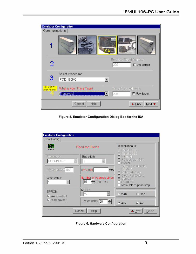
Figure 5. Emulator Configuration Dialog Box for the ISA
Figure 6. Hardware Configuration
Chapter 2. Installing and Configuring the Seehau SoftwareChapter 2. Installing and Configuring the Seehau SoftwareChapter 2. Installing and Configuring the Seehau SoftwareChapter 2. Installing and Configuring the Seehau Software
10101010 EMUL196–PC User Guide
4. When all the information has been entered, click Next to open the screen as shown inFigure 6. For information on the other settings, refer to the Intel handbook under the “ChipConfiguration Register” section.
5. The uP Clock is the internal CPU clock. This setting is used only for the calculation of thetrace timestamp. It has no effect on the operating speed of the emulation controller. The timeentered here should be the internal processor speed (not necessarily the crystal speed).
6. Click Next to enter the data. Click Yes at the Are you finished? prompt.
7. The Seehau Configuration Program creates Startup.bas and Seehau is now configured to runyour emulator.
8. The Seehau Configuration Program closes.
If you have completed these steps without any errors, you are ready to run the Seehau user inter-face after you have connected and powered up the EMUL196–PC emulator.
WARNING
The target power must never be on when the pod is powered off. To avoid damage, power the podand target on and off in the following sequence. To power up: (1) Power on the pod, then (2) Poweron the target. To power down: (1) Power off the target, then (2) power off the pod.
Purchasers of Emulator and Trace Boards
If you are purchasing the emulator board and the trace board, you might want to consider thefollowing points:
• You will need a PC with at least two ISA slots. These slots should be close enough to allowyou to connect the short ribbon cables that connect the boards or consider purchasing the HSPor USB box.
• It will be easier to connect the short ribbon cables before installation. Waiting until theboards are already installed can result in scraped and/or bloody knuckles due to therestricted work area.
• If you purchase the trace board after the emulator board, you should consider removing theemulator board, making the ribbon connections, and then installing the boards together.
EMUL196–PC User GuideEMUL196–PC User GuideEMUL196–PC User GuideEMUL196–PC User Guide
Edition 1, June 6, 2001 © 111111
Configuring Address Settings with WindowsOperating Systems
The following applies to all Windows operating systems:
• Default Address Ranges:
– Emulator Board: 200H– Trace Board: 208H
• Default Address Settings for the HSP Box:
No address conflict is possible when installing the HSP box with any Windows operating system.Use the default address ranges (listed above).
Skip to “Installing Emulator Boards” later in this chapter.
Configuring Address Settings for the Emulator and OptionalTrace BoardThe following sections provide details about configuring address settings for the emulator andoptional trace board for each Windows operating system. Refer to the section that covers yourspecific operating system.
Information about Windows NT InstallationWhen installing under Windows NT you will be changing the registry and installing our kernelmode driver. You must do this from an account with Administrator privileges.
One of the causes of the message Incorrect Parameter either in the system log or from the Devicesapplication is that there might be a device already installed with the address given for the emula-tor.
Known Device Driver ConflictsNohau is aware of potential device driver conflicts with certain network cards running onNovell/Netware networks. Problems have been reported with both 3COM ISA network cardsand some Novell network cards. Most of these problems have been experienced when runningWindows NT or Windows 2000 operating systems.
Possible SymptomsPossible SymptomsPossible SymptomsPossible Symptoms
• When starting Seehau, communication with the network stops. (You will be unable to accessresources on the network.)
• Seehau will not start.
A possible solution might be to change your network card. Nohau Technical Support has nottested all network cards, although some customers have reported that the following network cardshave resolved this conflict:
• Intel Ether Express Pro 10/100 ISA• 3COM Etherlink III (905B or later) 10/100 PCI• Bay Networks NetGear FA310TX 10/100 PCI
Chapter 2. Installing and Configuring the Seehau SoftwareChapter 2. Installing and Configuring the Seehau SoftwareChapter 2. Installing and Configuring the Seehau SoftwareChapter 2. Installing and Configuring the Seehau Software
12121212 EMUL196–PC User Guide
Configuring Address Settings with Windows 95/98
Checking Your PC for Default Address ConflictsChecking Your PC for Default Address ConflictsChecking Your PC for Default Address ConflictsChecking Your PC for Default Address Conflicts
1. Click the Start menu, and select Settings.
2. Click Control Panel.
3. Double-click System. The Systems Properties dialog box opens.
4. Click the Device Manager tab.
5. Click Properties.
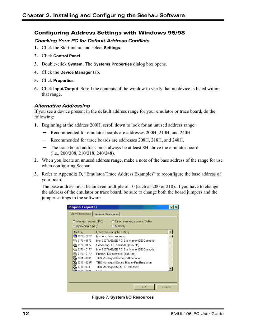
6. Click Input/Output. Scroll the contents of the window to verify that no device is listed withinthat range.
Alternative AddressingAlternative AddressingAlternative AddressingAlternative AddressingIf you see a device present in the default address range for your emulator or trace board, do thefollowing:
1. Beginning at the address 200H, scroll down to look for an unused address range:– Recommended for emulator boards are addresses 200H, 210H, and 240H.– Recommended for trace boards are addresses 208H, 218H, and 248H.– The trace board address must always be at least 8H above the emulator board
(i.e., 200/208, 210/218, 240/248).2. When you locate an unused address range, make a note of the base address of the range for use
when configuring Seehau.
3. Refer to Appendix D, “Emulator/Trace Address Examples” to reconfigure the base address ofyour board.The base address must be an even multiple of 10 (such as 200 or 210). If you have to changethe address of the emulator or trace board, be sure to change both the board jumpers and thejumper settings in the software.
Figure 7. System I/O Resources
EMUL196–PC User GuideEMUL196–PC User GuideEMUL196–PC User GuideEMUL196–PC User Guide
Edition 1, June 6, 2001 © 13 131313
Configuring Address Settings with Windows NT
• First, check your administrative privileges.
• Then check your PC for default address conflicts.
Checking Administrative PrivilegesChecking Administrative PrivilegesChecking Administrative PrivilegesChecking Administrative Privileges
1. Click the Start menu, and select Programs.
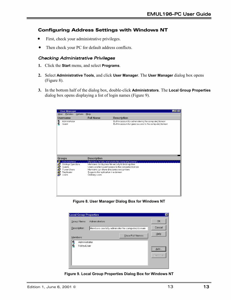
2. Select Administrative Tools, and click User Manager. The User Manager dialog box opens(Figure 8).
3. In the bottom half of the dialog box, double-click Administrators. The Local Group Propertiesdialog box opens displaying a list of login names (Figure 9).
Figure 8. User Manager Dialog Box for Windows NT
Figure 9. Local Group Properties Dialog Box for Windows NT
Chapter 2. Installing and Configuring the Seehau SoftwareChapter 2. Installing and Configuring the Seehau SoftwareChapter 2. Installing and Configuring the Seehau SoftwareChapter 2. Installing and Configuring the Seehau Software
14141414 EMUL196–PC User Guide
4. Look for your login name in the list of names. If your login name is not present, you are not setup with administrative privileges. Contact your System Administrator to update your privi-leges or give you the administrator’s password.
Checking Your PC for Default Address ConflictsChecking Your PC for Default Address ConflictsChecking Your PC for Default Address ConflictsChecking Your PC for Default Address Conflicts
1. Click the Start menu, and select Programs.
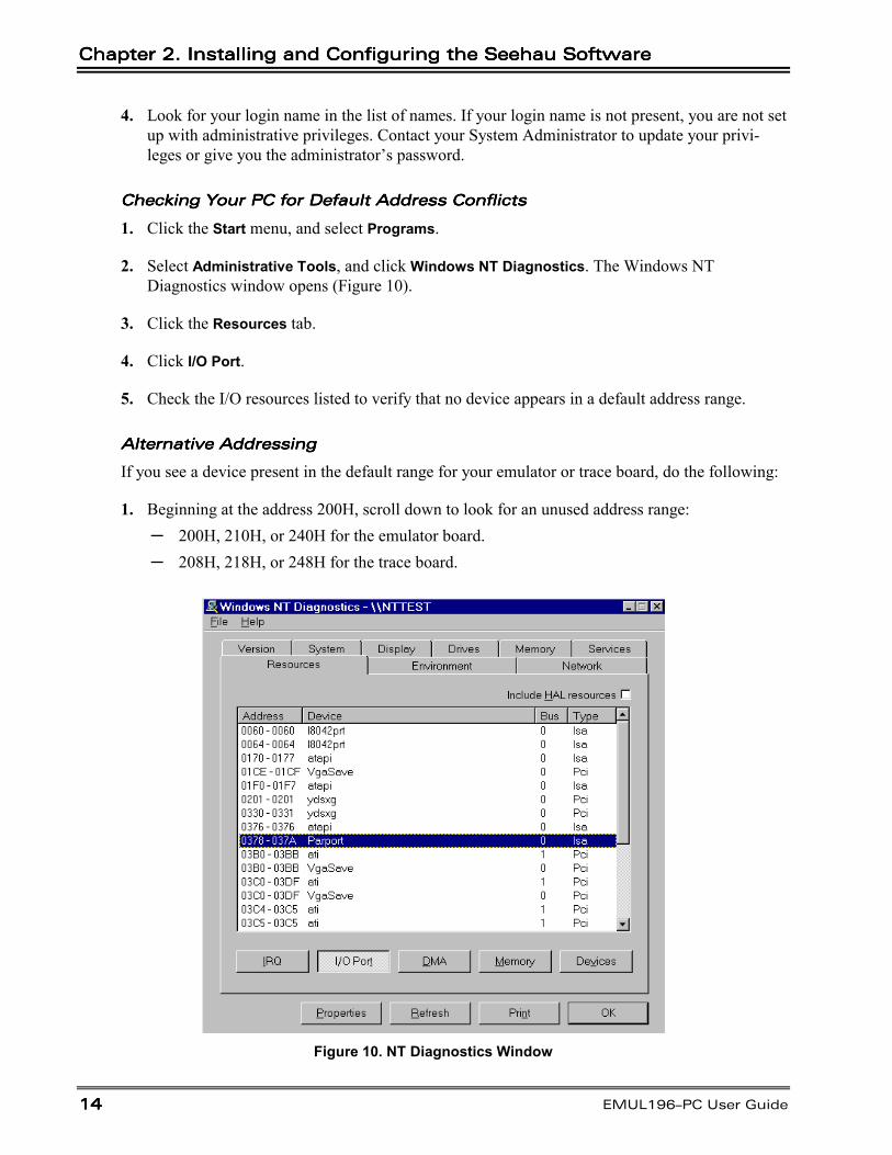
2. Select Administrative Tools, and click Windows NT Diagnostics. The Windows NTDiagnostics window opens (Figure 10).
3. Click the Resources tab.
4. Click I/O Port.
5. Check the I/O resources listed to verify that no device appears in a default address range.
Alternative AddressingAlternative AddressingAlternative AddressingAlternative Addressing
If you see a device present in the default range for your emulator or trace board, do the following:
1. Beginning at the address 200H, scroll down to look for an unused address range:– 200H, 210H, or 240H for the emulator board.– 208H, 218H, or 248H for the trace board.
Figure 10. NT Diagnostics Window
EMUL196–PC User GuideEMUL196–PC User GuideEMUL196–PC User GuideEMUL196–PC User Guide
Edition 1, June 6, 2001 © 15 151515
2. When you locate an unused address range, make a note of the base address of the range for usewhen configuring Seehau.
3. Refer to Appendix D, “Address Examples” to reconfigure the base address of your board.
Driver TroubleshootingDriver TroubleshootingDriver TroubleshootingDriver Troubleshooting
• If you get a Service or driver failed error message when rebooting, you probably have aresource conflict.
• If you get a create file failed error message upon execution, the device driver did notproperly start.
Nohau196 Device DriverNohau196 Device DriverNohau196 Device DriverNohau196 Device Driver
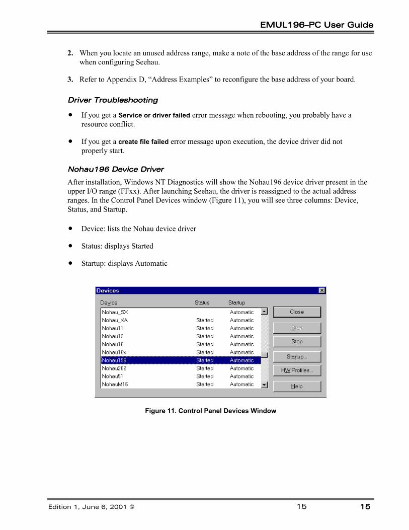
After installation, Windows NT Diagnostics will show the Nohau196 device driver present in theupper I/O range (FFxx). After launching Seehau, the driver is reassigned to the actual addressranges. In the Control Panel Devices window (Figure 11), you will see three columns: Device,Status, and Startup.
• Device: lists the Nohau device driver
• Status: displays Started
• Startup: displays Automatic
Figure 11. Control Panel Devices Window
Chapter 2. Installing and Configuring the Seehau SoftwareChapter 2. Installing and Configuring the Seehau SoftwareChapter 2. Installing and Configuring the Seehau SoftwareChapter 2. Installing and Configuring the Seehau Software
16161616 EMUL196–PC User Guide
Configuring Address Settings with Windows 2000
• First, check your administrative privileges.
• Then check your PC for default address conflicts.
Checking Administrative PrivilegesChecking Administrative PrivilegesChecking Administrative PrivilegesChecking Administrative Privileges
1. Click the Start menu, and select Settings. Click Control Panel.
2. From the Control Panel, double-click Users and Passwords. The Users and Passwordswindow opens (Figure 12).
3. Click the Advanced tab. Now click the Advanced button. The Local Users and Groupswindow opens (Figure 13).
Figure 12. Users and Passwords Window
Figure 13. Local Users and Groups Window
EMUL196–PC User GuideEMUL196–PC User GuideEMUL196–PC User GuideEMUL196–PC User Guide
Edition 1, June 6, 2001 © 171717
Figure 14. Local Users and Groups Window with Groups Folder
4. Click the Groups folder located in the left region of the window beneath Local Usersand Groups.
5. Double-click the Groups folder. A list of groups appears in the right region of the window(Figure 14).
6. Double-click Administrators. Your user name should be listed.
NoteIf you are not an administrator, ask your System Administrator to add you to this list.
Figure 15. Administrator Dialog Box
Chapter 2. Installing and Configuring the Seehau SoftwareChapter 2. Installing and Configuring the Seehau SoftwareChapter 2. Installing and Configuring the Seehau SoftwareChapter 2. Installing and Configuring the Seehau Software
18181818 EMUL196–PC User Guide
Checking Your PC for Default Address ConflictsChecking Your PC for Default Address ConflictsChecking Your PC for Default Address ConflictsChecking Your PC for Default Address Conflicts
1. Right-click the My Computer icon on your desktop, and select Properties. The SystemProperties window opens (Figure 16).
Figure 16. System Properties Window
Figure 17. Device Manager Window
EMUL196–PC User GuideEMUL196–PC User GuideEMUL196–PC User GuideEMUL196–PC User Guide
Edition 1, June 6, 2001 © 191919
2. Click the Hardware tab. Then click Device Manager. The Device Manager window opens(Figure 17).
3. In the Device Manager window, select the View menu. Then click Resources by Type.A window opens that shows the system resources (Figure 18).
4. Double-click Input/Output (I/O).
5. Check the I/O resources listed to verify that no device appears in the default address range forthese devices.
Figure 18. System Resources
Chapter 2. Installing and Configuring the Seehau SoftwareChapter 2. Installing and Configuring the Seehau SoftwareChapter 2. Installing and Configuring the Seehau SoftwareChapter 2. Installing and Configuring the Seehau Software
20202020 EMUL196–PC User Guide
Alternative AddressingAlternative AddressingAlternative AddressingAlternative Addressing
If you see a device present in the default address range for your emulator or trace board, do thefollowing:
1. Beginning at the address 200H, scroll down to look for an unused address range:– 200H, 210H, or 240H for the emulator board.– 208H, 218H, or 248H for the trace board.
2. When you locate an unused address range, make a note of the base address of the range for usewhen configuring Seehau.
3. Refer to Appendix D, “Address Examples” to reconfigure the base address of your board.
Driver TroubleshootingDriver TroubleshootingDriver TroubleshootingDriver Troubleshooting
For details, see Appendix A, “Troubleshooting Tips.”
• If you get a Service or driver failed error message when rebooting, you probably have aresource conflict.
• If you get a create file failed error message upon execution, the device driver did not properlystart. Review the steps in this section again. You can use Windows 2000 System Properties torecheck that your port address has no conflicts.
Nohau196 Device DriverNohau196 Device DriverNohau196 Device DriverNohau196 Device Driver
To verify that the Nohau196 device driver is properly installed, do the following:
1. From the Start menu, select Programs. Select Accessories, then System Tools.
2. Click System Information. The System Information window opens.
3. Double-click the Software Environment folder.
4. Double-click the Drivers folder. A list of active drivers appears. Refer to the Name columnand scroll down to nohau196.
5. Verify the driver is running. In the State column, you should see the word Running. In theStatus column, you should see OK.
EMUL196–PC User GuideEMUL196–PC User GuideEMUL196–PC User GuideEMUL196–PC User Guide
Edition 1, June 6, 2001 © 212121
Installing and Configuring theEmulator Board
1. If you are using the ISA card inside the PC, verify that the jumpers on the board are set for200H (the default address). If the computer has a game port or joy stick, it is typically locatedat address 201H. If this is the case, you will need to change the address of the emulator boardto an unused hardware address.
2. If you have the HSP box, connect the parallel cable to the parallel port of the PC or laptop.Also, connect the 5-volt power supply. The default parallel port is LPT1, located at the hard-ware address 378H within the PC.
3. Connect the five-foot ribbon cable from the emulator board to the pod.
Key Key Slot
Figure 19. Connecting the Emulator to Your Pod Board with the Ribbon Cable
NoteThe connectors of the ribbon cable are identical so it does not matter which end isconnected to the pod or the emulator board. Although the ribbon cable connectingthe emulator to the pod board is keyed, it is possible to force the key on the conec-tor the wrong way. Caution should be used when making the connection to ensurethat the key and slot line correctly.
Although not part of the emulator board, you might want to ensure the following steps as you hookup and configure the emulator board.
1. Verify the pod is stand-alone (not connected to the target), and that the power jumper is in-serted and the crystal jumpers are set for internal crystal.
2. There are four address jumpers: EA16, EA17, EA18, and EA19. The settings for these jumpersmust match the number of address lines selected when the hardware screen was configured.
Chapter 3. Installing and Configuring the Emulator BoardChapter 3. Installing and Configuring the Emulator BoardChapter 3. Installing and Configuring the Emulator BoardChapter 3. Installing and Configuring the Emulator Board
22222222 EMUL196–PC User Guide
NO
HA
U C
OR
P . E
MU
L-PC
/E
JP1 J2
JP3JP2
J4S/
N
REV. D
A3 A9
Pin 1
Figure 20. Rev. D Emulator Board
Installing the Emulator Board
The EMUL196–PC emulator board supports the following pod boards for different members of theIntel 80C196 microcontrollers:
• POD196–KR/NT
• POD196–NP/NU
• POD196–KC/KD
NotePods 196–CA/CB, 196–NP, and 196–EA have been discontinued. For informationabout these pod boards, see Appendix E, “Discontinued Pod Boards.”
As Intel introduces other members of the 80C196 family of microcontrollers, corresponding podboards will be introduced and supported by EMUL196–PC. Call Nohau Technical Support for thecurrent list of available pod boards and supported controllers.
The EMUL196–PC emulator board is an 8-bit PC card that fits into any ¾ length slot. It contains64K, 256K, or 1 MB of Shadow RAM, bus interface logic, trace board support logic, and the logicneeded to communicate with the pod. The jumpers on the emulator board control two things:
• The address used to communicate with the Host PC.
• The maximum communication rate of the target.
EMUL196–PC User GuideEMUL196–PC User GuideEMUL196–PC User GuideEMUL196–PC User Guide
Edition 1, June 6, 2001 © 232323
Emulator Installation Instructions
Setting the I/O Address Jumpers: J2
Each pair of pins in the address header J2 represents one bit in the 10-bit address. Address bits0, 1, and 2 represent addresses within the eight consecutive addresses, and they do not have pinpairs to represent them. This leaves six address bits (pin pairs) to set with jumpers: A3 through A9.Shorting two pins represents a zero in the address. A pair of pins with no jumper representsa one.
The emulator board address jumpers have been factory preset to 200H for a typical system. Thefollowing table shows how a typical system uses its address locations. If your system is presentlyusing location 200H, you must find an alternate address location and make appropriate changes tothe jumpers and software. If your emulator board is in an external HSP/USB box, you should usethe default address regardless of the I/O address being used in the computer.
Typical PC I/O Addresses
Hex Location Typical Use000 – 0FF Used by system
1F0 – 1F8 Fixed disk
200 – 207 Game adapter
210 – 213 Expansion unit
278 – 27F Parallel printer Port 2
2F8 – 2FF Secondary asynchronous printer adaper
300 – 31F Prototype card
320 – 323 Fixed disk controller
360 – 36F Reserved
378 – 37A Printer adapter
380 – 38F Alternate binary synchronous communications adapter, SDLC adapter
3A0 – 3AF Primary binary synchronous communications adapter
3B0 – 3BF Monochromatic display and printer adapter
3C0 – 3CF Reserved
3D0 – 3DF Color/graphics monitor adapter
3F0 – 3F7 Floppy disk controller
3F8 –3FF Primary asynchronous printer adapter
If the current emulator board address conflicts with any other hardware, find free address spacebetween 210 and 3FFH. The emulator board requires eight consecutive addresses. If you changethe address and/or memory jumpers, the software address settings must also be changed.
Chapter 3. Installing and Configuring the Emulator BoardChapter 3. Installing and Configuring the Emulator BoardChapter 3. Installing and Configuring the Emulator BoardChapter 3. Installing and Configuring the Emulator Board
24242424 EMUL196–PC User Guide
200 HexPC Bus AddressPin labels
Jumper Settings
A3 A9208 Hex
A3 A9300 HexPC Bus Address
Pin labels
Jumper Settings
A3 A93F8 Hex
A3 A9
Factory Default
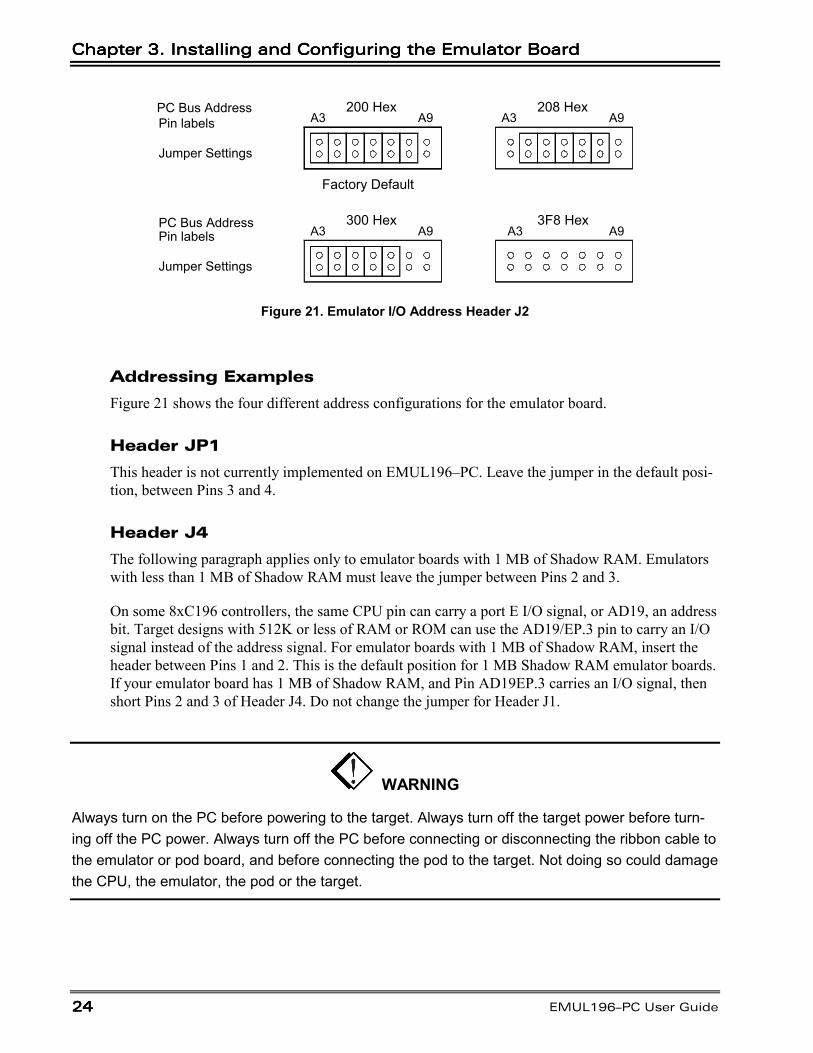
Figure 21. Emulator I/O Address Header J2
Addressing Examples
Figure 21 shows the four different address configurations for the emulator board.
Header JP1
This header is not currently implemented on EMUL196–PC. Leave the jumper in the default posi-tion, between Pins 3 and 4.
Header J4
The following paragraph applies only to emulator boards with 1 MB of Shadow RAM. Emulatorswith less than 1 MB of Shadow RAM must leave the jumper between Pins 2 and 3.
On some 8xC196 controllers, the same CPU pin can carry a port E I/O signal, or AD19, an addressbit. Target designs with 512K or less of RAM or ROM can use the AD19/EP.3 pin to carry an I/Osignal instead of the address signal. For emulator boards with 1 MB of Shadow RAM, insert theheader between Pins 1 and 2. This is the default position for 1 MB Shadow RAM emulator boards.If your emulator board has 1 MB of Shadow RAM, and Pin AD19EP.3 carries an I/O signal, thenshort Pins 2 and 3 of Header J4. Do not change the jumper for Header J1.
WARNING
Always turn on the PC before powering to the target. Always turn off the target power before turn-ing off the PC power. Always turn off the PC before connecting or disconnecting the ribbon cable tothe emulator or pod board, and before connecting the pod to the target. Not doing so could damagethe CPU, the emulator, the pod or the target.
EMUL196–PC User GuideEMUL196–PC User GuideEMUL196–PC User GuideEMUL196–PC User Guide
Edition 1, June 6, 2001 © 252525
Installing the Emulator Board into the ISA Slot
After the jumpers are set, do the following with the PC power off:
1. Remove the PC cover.
2. Insert the emulator board into any free slot.
3. Close the PC cover.
4. Connect the ribbon cable to the emulator board.
5. Connect the pod to the ribbon cable.
Shadow RAM
The EMUL196–PC emulator board contains either 64K, 256K, or 1 MB of static RAM used toshadow or duplicate the contents of the target RAM. Every time the CPU generates a WRITE buscycle while running the target application, the pod captures the address/data pair and the emulatorboard writes that data to the same address in Shadow RAM. The Seehau application can simulta-neously read Shadow RAM. This allows the software to display values written by the applicationwithout interrupting emulation.
NoteShadow RAM will capture external data writes while you are running your code.Shadow RAM will not capture the bus activity while the pod is executing monitorcode. Loading code, filling memory, and editing registers will not update ShadowRAM.
Notice the emulator board has 64K of Shadow RAM, and the application data area RAM is larger.The emulator board has 64K of Shadow RAM. If your microcontroller accesses addresses above64K, the data WRITE address will be masked off to 16 bits when reaching the Shadow RAM. TheShadow RAM address logic strips off the bits above bit 15. The Shadow RAM address 100H willbe modified by WRITEs to application RAM addresses 100H, 10100H, and 20100H. Similarly, ifthe emulator has 256K of Shadow RAM, WRITEs to application RAM addresses 100H, 40100H,and 80100H will all update the same Shadow RAM byte (at address 100H). This is true for emu-lation RAM, RAM on the target, or even memory-mapped I/O devices. Ordering an emulatorboard with 256K of Shadow RAM will minimize the amount of overlaid RAM. However, targetsthat have more than 256K of RAM, overlaying will still be possible. Ordering an emulator boardwith 1 MB of Shadow RAM will eliminate this problem for all 8xC196 applications.
Chapter 3. Installing and Configuring the Emulator BoardChapter 3. Installing and Configuring the Emulator BoardChapter 3. Installing and Configuring the Emulator BoardChapter 3. Installing and Configuring the Emulator Board
26262626 EMUL196–PC User Guide
Quick-Save Settings
Due to the instability of PCs and operating systems, it is important to take precautions after settingup your hardware and software. Rather than wait until you have finished doing your tests on thetarget system you might want to save the emulator settings to avoid unnecessary repetition in caseof system failure. The quick way to avoid this problem is to do the following:
1. To save the emulator configuration, click the Config option and select Environment.
2. From the Environment Configuration menu, check the Use Start-up Dialog? (this promptsyou to select the preferred startup file when selected) under the Preferences tab. This optionis located in the Miscellaneous section.
3. Select Apply or OK. The Environment Configuration dialog box will close.
4. Exit from the Seehau software.
5. The Save Settings dialog box opens where you can choose the filename for the newly createdmacro. Enter a filename of your choosing and click Save.
The macro is ready to use and will accurately recreate your emulator configuration settings.
EMUL196–PC User GuideEMUL196–PC User GuideEMUL196–PC User GuideEMUL196–PC User Guide
Edition 1, June 6, 2001 © 272727
Installing and Configuring theTrace Board
Hardware Description
The trace board is a full length ISA-style bus card and contains the RAM needed to record arecord of the data accessed and instructions executed. The emulator board has the logic and con-nectors necessary to support the trace board. It can occupy any 8- or 16-bit slot as long as the tworibbon cables can reach from the emulator card to the trace card. When inserted into a 16-bit slot,it connects with the additional power and ground lines in the other connector on the motherboard.The card includes 104 bits of RAM for each trace record. There are two types of trace boards forthe EMUL196–PC: standard and data. Standard trace boards are available with 32K of trace mem-ory, data trace boards are available with either 128K or 512K of trace memory.
Installation Instructions
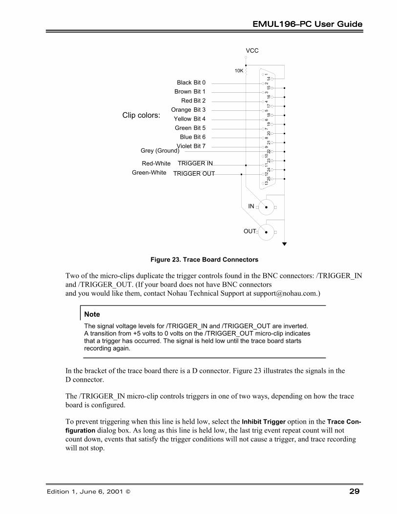
The trace board includes three connectors on the back for inputting and outputting signals. Figure23 shows how the connectors for the DB-25 connector and the two BNC connectors are wired.
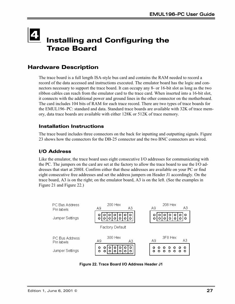
I/O Address
Like the emulator, the trace board uses eight consecutive I/O addresses for communicating withthe PC. The jumpers on the card are set at the factory to allow the trace board to use the I/O ad-dresses that start at 208H. Confirm either that these addresses are available on your PC or findeight consecutive free addresses and set the address jumpers on Header J1 accordingly. On thetrace board, A3 is on the right; on the emulator board, A3 is on the left. (See the examples inFigure 21 and Figure 22.)
Figure 22. Trace Board I/O Address Header J1
Chapter 4. Installing and Configuring the Trace BoardChapter 4. Installing and Configuring the Trace BoardChapter 4. Installing and Configuring the Trace BoardChapter 4. Installing and Configuring the Trace Board
28282828 EMUL196–PC User Guide
After the trace board address jumpers are set, do the following:
1. Turn off the PC power or HSP/USB box power, remove the cover, and slide the board intothe chosen ISA slot (the ISA slots must be next to each other). Make sure the board is fullyinserted. There are two identical ribbon cables. Due to the length and shape of the cables, itis impossible to attach both cables to the incorrect connector.
NoteIt might be easier to remove the emulator board from the chassis and attach thecables before reinserting the boards into their respective slots. The tightness aroundthe boards and the pins can result in skinned or bloody knuckles if not careful.
2. Make sure the pins are fully inserted into the connectors so there are no exposed pins, thereare no twists in either cable, and the cables do not cross. Be certain the connectors are not off-set vertically or horizontally. The most common error is to insert only one row of pins into theconnector. This can damage either of the boards. Double-check all four connectors for any ex-posed pins before continuing.
3. After the ribbon cables are attached, close the PC or HSP/USB box cover, power up the PC orHSP/USB box, and start Windows.
4. Start the Seehau196 program.
5. Verify that the Seehau196 configuration is set up to recognize the trace board. This is done inthe Seehau196 Configuration Program.
6. Verify that Trace Type indicates Trace (Yes), and the I/O address is correct. This address boxneeds to contain the same address as the jumpers in Header J1 as mentioned previously.
NoteIf the hex address was changed for the emulator board, the hex address for thetrace board must be changed accordingly.
External Inputs and ControlsThe trace board records eight external digital inputs with every bus cycle. These signals are inputthrough the DB-25 (also called a D connector) connector on the back of the trace board. To sim-plify providing these signals to the trace board use the color-coded set of micro-clips providedwith the trace board. (The 25-conductor ribbon cable is wired straight through and can be used toextend the reach of the micro-clips.)
NoteAs external inputs and controls are sampled at every frame, you cannot expecthigher time resolution than the sample frame rate.
EMUL196–PC User GuideEMUL196–PC User GuideEMUL196–PC User GuideEMUL196–PC User Guide
Edition 1, June 6, 2001 © 292929
VCC
TRIGGER IN
TRIGGER OUT
2324
2522
2120
1918
1716
153
26
814
1213
111
57
94
10
Grey (Ground)
Green-WhiteRed-White
Clip colors:
10K
IN
OUT
Bit 4Yellow
Bit 1BrownBit 2RedBit 3Orange
Bit 5Green
Bit 0Black
Bit 6BlueBit 7Violet
Figure 23. Trace Board Connectors
Two of the micro-clips duplicate the trigger controls found in the BNC connectors: /TRIGGER_INand /TRIGGER_OUT. (If your board does not have BNC connectorsand you would like them, contact Nohau Technical Support at [email protected].)
NoteThe signal voltage levels for /TRIGGER_IN and /TRIGGER_OUT are inverted.A transition from +5 volts to 0 volts on the /TRIGGER_OUT micro-clip indicatesthat a trigger has occurred. The signal is held low until the trace board startsrecording again.
In the bracket of the trace board there is a D connector. Figure 23 illustrates the signals in theD connector.
The /TRIGGER_IN micro-clip controls triggers in one of two ways, depending on how the traceboard is configured.
To prevent triggering when this line is held low, select the Inhibit Trigger option in the Trace Con-figuration dialog box. As long as this line is held low, the last trig event repeat count will notcount down, events that satisfy the trigger conditions will not cause a trigger, and trace recordingwill not stop.
Chapter 4. Installing and Configuring the Trace BoardChapter 4. Installing and Configuring the Trace BoardChapter 4. Installing and Configuring the Trace BoardChapter 4. Installing and Configuring the Trace Board
30303030 EMUL196–PC User Guide
You can also select the Assert Trigger option. The transition to ground on the /TRIGGER_IN linewill cause a trigger on the trace board and stop trace recording. Similar to a trigger caused by a buscycle, this external trigger can cause a hardware break if the Break on Trig option is selected. (Onthe Rev. C boards, the /TRIGGER_IN signal is a trigger inhibit signal.)
Tracing Overview
A trace history is a time ordered recording of bus cycles (with some other helpful information).Events that do not affect the CPU external bus, such as testing a CPU internal register, are not re-corded. Events that do affect the bus will only be recorded if the trace setup is instructed to recordthose types of events. All tracing emulators record bus events and not actual instruction execution,so they must have some way to process the instruction pipeline. The trace board includes pipelinedecoding and marks opcode fetches that are not executed. Therefore, the display software canshow the trace records as though the pipeline does not exist. Optionally, the software can displaythe uncorrected bus cycles just as recorded.
Trace Modes
To allow selective recording, three trace modes are available:
• Normal Mode—records everything.
• Window Mode—allows you to turn on or turn off recording.
• Filer Mode—lets you specify selected address to be recorded
Normal ModeNormal ModeNormal ModeNormal Mode
Tracing starts automatically every time emulation starts. Single-stepping turns on the trace re-cording during user code execution. The trace buffer continues to collect records until recording isstopped. Tracing is stopped in one of the following ways:
• Automatically by a trigger
• Stopping emulation by clicking Start or Stop Emulator
• Stopping trace by clicking Start or Stop Trace
Any one trigger can optionally generate a hardware breakpoint.
The trace buffer is a ring buffer that collects new records and replaces old records until recordingis stopped. When tracing starts, the buffer is cleared. After recording a single-step, the trace bufferonly contains the records for that one instruction or source line. As long as trace recording contin-ues, records are added to the buffer. Once the buffer is full, the new records overwrite the oldestrecords.
EMUL196–PC User GuideEMUL196–PC User GuideEMUL196–PC User GuideEMUL196–PC User Guide
Edition 1, June 6, 2001 © 313131
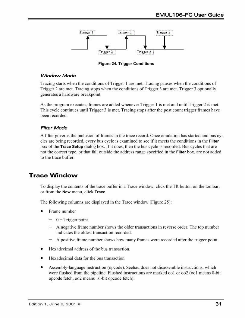
Figure 24. Trigger Conditions
Window ModeWindow ModeWindow ModeWindow Mode
Tracing starts when the conditions of Trigger 1 are met. Tracing pauses when the conditions ofTrigger 2 are met. Tracing stops when the conditions of Trigger 3 are met. Trigger 3 optionallygenerates a hardware breakpoint.
As the program executes, frames are added whenever Trigger 1 is met and until Trigger 2 is met.This cycle continues until Trigger 3 is met. Tracing stops after the post count trigger frames havebeen recorded.
Filter ModeFilter ModeFilter ModeFilter Mode
A filter governs the inclusion of frames in the trace record. Once emulation has started and bus cy-cles are being recorded, every bus cycle is examined to see if it meets the conditions in the Filterbox of the Trace Setup dialog box. If it does, then the bus cycle is recorded. Bus cycles that arenot the correct type, or that fall outside the address range specified in the Filter box, are not addedto the trace buffer.
Trace Window
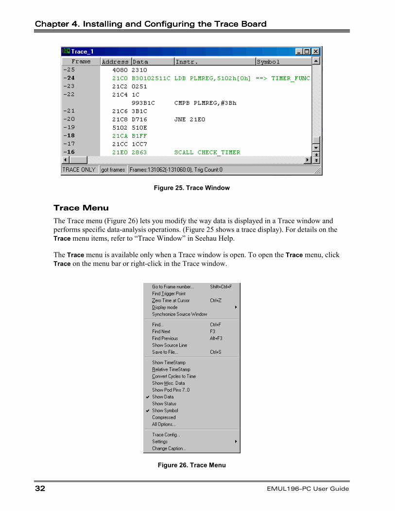
To display the contents of the trace buffer in a Trace window, click the TR button on the toolbar,or from the New menu, click Trace.
The following columns are displayed in the Trace window (Figure 25):
• Frame number
– 0 = Trigger point– A negative frame number shows the older transactions in reverse order. The top number
indicates the oldest transaction recorded.– A positive frame number shows how many frames were recorded after the trigger point.
• Hexadecimal address of the bus transaction.
• Hexadecimal data for the bus transaction
• Assembly-language instruction (opcode). Seehau does not disassemble instructions, whichwere flushed from the pipeline. Flushed instructions are marked oo1 or oo2 (oo1 means 8-bitopcode fetch, oo2 means 16-bit opcode fetch).
Chapter 4. Installing and Configuring the Trace BoardChapter 4. Installing and Configuring the Trace BoardChapter 4. Installing and Configuring the Trace BoardChapter 4. Installing and Configuring the Trace Board
32323232 EMUL196–PC User Guide
Figure 25. Trace Window
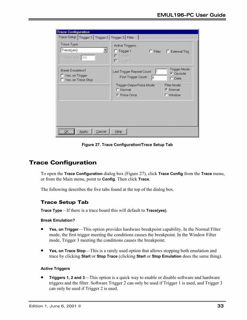
Trace Menu
The Trace menu (Figure 26) lets you modify the way data is displayed in a Trace window andperforms specific data-analysis operations. (Figure 25 shows a trace display). For details on theTrace menu items, refer to “Trace Window” in Seehau Help.
The Trace menu is available only when a Trace window is open. To open the Trace menu, clickTrace on the menu bar or right-click in the Trace window.
Figure 26. Trace Menu
EMUL196–PC User GuideEMUL196–PC User GuideEMUL196–PC User GuideEMUL196–PC User Guide
Edition 1, June 6, 2001 © 333333
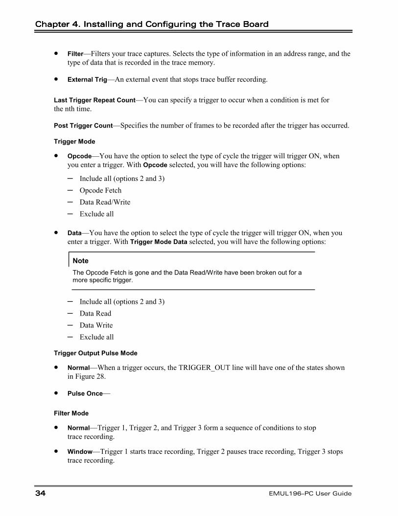
Figure 27. Trace Configuration/Trace Setup Tab
Trace Configuration
To open the Trace Configuration dialog box (Figure 27), click Trace Config from the Trace menu,or from the Main menu, point to Config. Then click Trace.
The following describes the five tabs found at the top of the dialog box.
Trace Setup Tab
Trace Type—If there is a trace board this will default to Trace(yes).
Break Emulation?
• Yes, on Trigger—This option provides hardware breakpoint capability. In the Normal Filtermode, the first trigger meeting the conditions causes the breakpoint. In the Window Filtermode, Trigger 3 meeting the conditions causes the breakpoint.
• Yes, on Trace Stop—This is a rarely used option that allows stopping both emulation andtrace by clicking Start or Stop Trace (clicking Start or Stop Emulation does the same thing).
Active Triggers
• Triggers 1, 2 and 3—This option is a quick way to enable or disable software and hardwaretriggers and the filter. Software Trigger 2 can only be used if Trigger 1 is used, and Trigger 3can only be used if Trigger 2 is used.
Chapter 4. Installing and Configuring the Trace BoardChapter 4. Installing and Configuring the Trace BoardChapter 4. Installing and Configuring the Trace BoardChapter 4. Installing and Configuring the Trace Board
34343434 EMUL196–PC User Guide
• Filter—Filters your trace captures. Selects the type of information in an address range, and thetype of data that is recorded in the trace memory.
• External Trig—An external event that stops trace buffer recording.
Last Trigger Repeat Count—You can specify a trigger to occur when a condition is met forthe nth time.
Post Trigger Count—Specifies the number of frames to be recorded after the trigger has occurred.
Trigger Mode
• Opcode—You have the option to select the type of cycle the trigger will trigger ON, whenyou enter a trigger. With Opcode selected, you will have the following options:
– Include all (options 2 and 3)– Opcode Fetch– Data Read/Write– Exclude all
• Data—You have the option to select the type of cycle the trigger will trigger ON, when youenter a trigger. With Trigger Mode Data selected, you will have the following options:
NoteThe Opcode Fetch is gone and the Data Read/Write have been broken out for amore specific trigger.
– Include all (options 2 and 3)– Data Read– Data Write– Exclude all
Trigger Output Pulse Mode
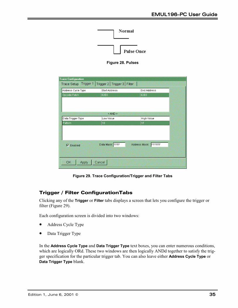
• Normal—When a trigger occurs, the TRIGGER_OUT line will have one of the states shownin Figure 28.
• Pulse Once—
Filter Mode
• Normal—Trigger 1, Trigger 2, and Trigger 3 form a sequence of conditions to stoptrace recording.
• Window—Trigger 1 starts trace recording, Trigger 2 pauses trace recording, Trigger 3 stopstrace recording.
EMUL196–PC User GuideEMUL196–PC User GuideEMUL196–PC User GuideEMUL196–PC User Guide
Edition 1, June 6, 2001 © 353535
Figure 28. Pulses
Figure 29. Trace Configuration/Trigger and Filter Tabs
Trigger / Filter ConfigurationTabs
Clicking any of the Trigger or Filter tabs displays a screen that lets you configure the trigger orfilter (Figure 29).
Each configuration screen is divided into two windows:
• Address Cycle Type
• Data Trigger Type
In the Address Cycle Type and Data Trigger Type text boxes, you can enter numerous conditions,which are logically ORd. These two windows are then logically ANDd together to satisfy the trig-ger specification for the particular trigger tab. You can also leave either Address Cycle Type orData Trigger Type blank.
Chapter 4. Installing and Configuring the Trace BoardChapter 4. Installing and Configuring the Trace BoardChapter 4. Installing and Configuring the Trace BoardChapter 4. Installing and Configuring the Trace Board
36363636 EMUL196–PC User Guide
Entering Addresses and Data
By right clicking in the Trace Configuration window, a dialog box opens with the followingchoices:
• Add
• Remove
• Edit
You must have a line selected to exercise the Remove or Edit options. Alternatively, you can pressDEL on the keyboard to remove a line, or double-click the line to edit.
The Add and Edit options display slightly different windows depending on the trigger modeselected in the Trace Setup tab.
Figure 30. Address Cycle Type/Opcode Trigger Mode
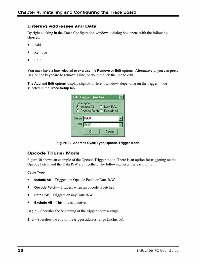
Opcode Trigger Mode
Figure 30 shows an example of the Opcode Trigger mode. There is an option for triggering on theOpcode Fetch, and the Data R/W are together. The following describes each option:
Cycle Type
• Include All—Triggers on Opcode Fetch or Data R/W.
• Opcode Fetch—Triggers when an opcode is fetched.
• Data R/W—Triggers on any Data R/W.
• Exclude All—This line is inactive.
Begin—Specifies the beginning of the trigger address range.
End—Specifies the end of the trigger address range (inclusive).
EMUL196–PC User GuideEMUL196–PC User GuideEMUL196–PC User GuideEMUL196–PC User Guide
Edition 1, June 6, 2001 © 373737
Figure 31. Address Cycle Type/Data Trigger Mode
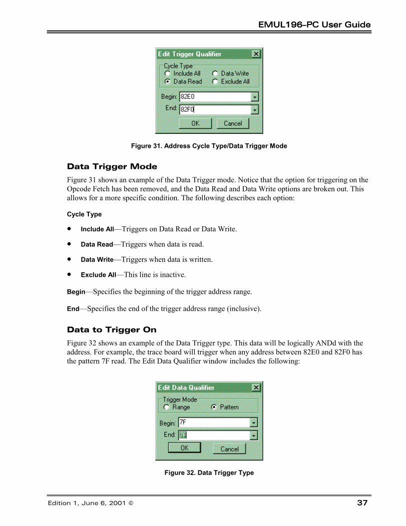
Data Trigger Mode
Figure 31 shows an example of the Data Trigger mode. Notice that the option for triggering on theOpcode Fetch has been removed, and the Data Read and Data Write options are broken out. Thisallows for a more specific condition. The following describes each option:
Cycle Type
• Include All—Triggers on Data Read or Data Write.
• Data Read—Triggers when data is read.
• Data Write—Triggers when data is written.
• Exclude All—This line is inactive.
Begin—Specifies the beginning of the trigger address range.
End—Specifies the end of the trigger address range (inclusive).
Data to Trigger On
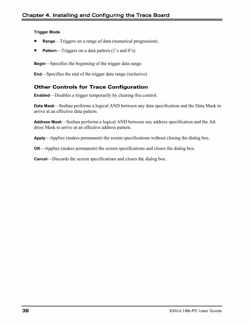
Figure 32 shows an example of the Data Trigger type. This data will be logically ANDd with theaddress. For example, the trace board will trigger when any address between 82E0 and 82F0 hasthe pattern 7F read. The Edit Data Qualifier window includes the following:
Figure 32. Data Trigger Type
Chapter 4. Installing and Configuring the Trace BoardChapter 4. Installing and Configuring the Trace BoardChapter 4. Installing and Configuring the Trace BoardChapter 4. Installing and Configuring the Trace Board
38383838 EMUL196–PC User Guide
Trigger Mode
• Range—Triggers on a range of data (numerical progression).
• Pattern—Triggers on a data pattern (1’s and 0’s).
Begin—Specifies the beginning of the trigger data range.
End—Specifies the end of the trigger data range (inclusive).
Other Controls for Trace Configuration
Enabled—Disables a trigger temporarily by clearing this control.
Data Mask—Seehau performs a logical AND between any data specification and the Data Mask toarrive at an effective data pattern.
Address Mask—Seehau performs a logical AND between any address specification and the Ad-dress Mask to arrive at an effective address pattern.
Apply—Applies (makes permanent) the screen specifications without closing the dialog box.
OK—Applies (makes permanent) the screen specifications and closes the dialog box.
Cancel—Discards the screen specifications and closes the dialog box.
EMUL196–PC User GuideEMUL196–PC User GuideEMUL196–PC User GuideEMUL196–PC User Guide
Edition 1, June 6, 2001 © 393939
Accessories and Adapters
Types of Adapters
There are many different types of adapters available for the 196 pods. Before you connect theadapter to the pod, you must verify the adapter’s orientation in reference to the pod to avoid dam-age to the pod and target board. Adapter orientation in reference to the pod’s Pin 1 can be 0, 90, or180 degrees.
The POD196 has several adapters that are used in attaching a target board to the pod:
• PLCC
• Pin Grid Array
• Clip-Over
• Surface Mount QFP
• Surface Mount SQFP
Verifying the Orientation of Your Adapter
To verify the orientation of your adapter, start the Seehau196 Adapter Program (included on theSeehau software CD). You can access this program several ways:
1. Click on the Start menu
2. Move your cursor over Programs until it is highlighted.
3. The available programs will appear to one side.
4. Find the program labeled Seehau 196 and move the cursor over it until it is highlighted.
5. A secondary menu will appear
6. Move your cursor over the option labeled View Adapters and click on it.
7. The program will start.
8. Maximize the box that appears and then click on the down arrow next to the list of adapters.
9. A list of all the adapters will appear.
10. Click on the adapter that you are interested and a picture will appear.

Chapter 5. Accessories and AdaptersChapter 5. Accessories and AdaptersChapter 5. Accessories and AdaptersChapter 5. Accessories and Adapters
40404040 EMUL196–PC User Guide
Creating a Shortcut to PicView
If you would like, you can also put an icon on your desktop rather than follow the previous proce-dure. To create this icon, follow this procedure if you did not move the icon to your desktop whenthe Seehau software was first installed.
1. Start Windows Explorer.
2. Find the Nohau directory and then the Seehau196 subdirectory (C:/Nohau/Seehau196).
3. Click on the Seehau196 subdirectory to highlight the files and subdirectories.
4. Find the file called PicView.exe and right-click on it.
5. A secondary menu will appear to the side.
6. Move your cursor over the option Create Shortcut and click on it.
7. At the end of the list of files in the directory, a new file called Shortcut to PicView.exe willappear.
8. Drag the file onto your desktop.
9. Rename Shortcut to PicView.exe to an appropriate name (right click on the file and Renamethe file).
10. When the program starts follow the procedures from items number 8, 9, and 10 from theprevious list.
EMUL196–PC User GuideEMUL196–PC User GuideEMUL196–PC User GuideEMUL196–PC User Guide
Edition 1, June 6, 2001 © 414141
Installing and Configuring thePod Board
Overview
Every pod is a fully functional, stand-alone 8xC196 board, with a processor, RAM, a crystal,PROM, and logic.
When you click Reset, the emulator pulls the /RST line low, resetting the controller. When the/RST line is released the controller begins executing instructions that allow the emulator board tocommunicate with the pod. The controller will continue to execute monitor code until you clickStep, Go, or from the Run menu, click Reset, then Go.
When you click Break, a specific kind of nonmaskable interrupt occurs, the return address ispushed on the stack, the program counter is loaded with the monitor vector, and it continues to runat the new address.
When sections of memory are displayed on your screen, the controller actually reads the memorylocations and sends the values back to the emulator board in your PC.
NoteIf you are running user code, target power can be turned OFF/ON to emulate poweron if /RESET is held low during power off.
Features Common to All Pod Boards
Stack Pointer
Because the emulator pushes the return address on the stack, the Stack Pointer must point to validmemory. There must be room on the stack for two bytes (or four bytes for users of chips withlarger addressable ranges) to hold the address.
CAUTION
In addition, there is a lower limit to the stack pointer. The stack pointer must have a value greaterthan 0x50, or else your register contents cannot be saved correctly.
Chapter 6. Installing and Configuring the Pod BoardsChapter 6. Installing and Configuring the Pod BoardsChapter 6. Installing and Configuring the Pod BoardsChapter 6. Installing and Configuring the Pod Boards
42424242 EMUL196–PC User Guide
Indicator Lights
The pod boards contain four lights: Halt, Reset, Run, and User.
Halt Light—indicates when the target asserts the HLD signal. This light is connected directly tothe port pin, which drives this signal. The port pin can also be configured as an I/O pin. If config-ured as HLDA#, then this light indicates when the target asserts the HLD signal. If configured asan I/O pin, then the light will toggle according to the signal.
NoteIf using the HLD pin as low speed I/O, disregard the light.
Reset Light—indicates when the emulator resets the controller.
Run Light—indicates when the controller is executing user code (as opposed to monitor).
User Light—indicates the state of any signal on the pod or target by connecting a wire from thedesired signal to the test point labeled TP1. The user light indicates when the test point is broughtlow.
How to Simultaneously Stop Code Execution onTwo Emulators
At the edge of the pod board there are two test points called BRK_IN and BRK_OUT. TheBRK_OUT test point will show logic low when the user code stops. The BRK_IN test point, ifforced to logic low, will make the user code stop. With two emulator systems, you can connectBRK_OUT from one pod to BRK_IN on the other pod to make the two-emulator systems stopuser code execution simultaneously.
Trace Input Pins
Next to the indicator lights and the test point is an array of eight pins labeled Trace. These pins canbe connected to any logic signal and will record the state of that signal with every trace record.(Pins 0 through 3 are sampled with the address, on the falling edge of ALE.) Pins 4 through 7 aresampled with the data, on the rising edge of the RD/WR strobes. For more information about dis-playing these bits and TRIGGER_IN/TRIGGER_OUT, refer to Chapter 4, “Installing and Config-uring the Trace Board” in this guide.
Resource Selection
If the same resource appears on both the target board and the pod board, there can be interferencethat will prevent correct emulation. The only way to avoid this conflict is to remove or disable ei-ther the target or the pod resource for all the resources that appear on both.
EMUL196–PC User GuideEMUL196–PC User GuideEMUL196–PC User GuideEMUL196–PC User Guide
Edition 1, June 6, 2001 © 434343
When the pod is connected to a target that has no power supply the pod can supply +5V to the tar-get limited by your PC supply capacity and the target’s sensitivity to under voltage. If the targethas its own power supply, remove the jumper on the PWR header. If you do not remove thejumper, it is possible to damage the target power supply, the PC power supply or both.
If your target has a crystal operating at a different frequency from the crystal on your pod, youmight want to use the target crystal instead of the pod crystal. To use the target crystal, find thetwo headers labeled TARGET/POD near the pod crystal and place the two jumpers so that they areon the TARGET side. This will disconnect the pod crystal from the controller on the pod and al-low the pod controller to use the crystal on the target.
Power
When the pod is connected to a target that has no power supply, the pod can supply +5 volts to thetarget limited by your PC supply capacity and target's sensitivity to under-voltage. See individualpods for maximum current.
WARNING
If the target has its own power supply, remove the jumper on the PWR header. If you do not, it ispossible to damage either the target power supply or the power supply in your PC.
XTAL
If your target has a crystal operating at a speed different from the frequency on your pod, youmight want to use the target crystal instead of the pod crystal. To use the target crystal, find thetwo headers labeled TARGET/POD near the pod crystal and place the two jumpers on the targetside. This disconnects the pod crystal from the controller on the pod and allows the pod controllerto use the crystal on the target.
Microcontroller
EMUL196–PC uses a special emulation controller to emulate the 80C196. This special chip hasextra pins that give the emulator extra features. The emulation controller can map memory, haltexecution, and set breakpoints. This is why your program must execute in the controller on the podand not in the controller on your target board.
Chapter 6. Installing and Configuring the Pod BoardsChapter 6. Installing and Configuring the Pod BoardsChapter 6. Installing and Configuring the Pod BoardsChapter 6. Installing and Configuring the Pod Boards
44444444 EMUL196–PC User Guide
Clip-Over Adapter
WARNING
Due to the possibility that the system can become unreliable when applying an adapter, Nohaudoes not recommend their use. In certain cases, it will be necessary for some customers to usethese adapters due to space restrictions. As such, Nohau will sell the necessary adapters for thosecustomers who really need them.
Most adapters fit between the pod and the target board, replacing the target controller. When usingthe clip-over adapter, you must leave the controller on the target so you can clip to it. The pod willautomatically disable the controller in the target (if you have the Once jumper in place). For moreinformation about how to use the clip-over adapter, refer to the “View Adapter” software providedwith the Seehau CD and see Chapter 5, “Accessories and Adapters” in this guide.
Summary of Hardware Configuration
• RAM—can be mapped to the target.
• Target Crystal—can be selected by moving JP7 and JP10 to the target side of the header.
• Target Serial Port—can be selected by removing the RXD jumper (J1).
• Target Power Supply—can be selected by removing the jumper from the PWR headeron the pod.
WARNING
The black wire with the micro-clip is a ground wire, which is helpful for ensuring that the pod andtarget grounds are at the same potential. It is recommend you attach this clip to a grounded pointon your target before attaching the pod to the target.
Memory Map Configuration Requirements
The emulator software allows you to map any address to either the pod or the target. However, Ifyou map all RAM to the target, there are three special addresses that the emulator needs: 18H,2010H, and 2012H. The simplest suggestion is to leave those three addresses mapped to the pod. Ifyou must map addresses 2010H and 2012H to the target, those addresses on your target must con-tain the value 0019H to support software breakpoints.
EMUL196–PC User GuideEMUL196–PC User GuideEMUL196–PC User GuideEMUL196–PC User Guide
Edition 1, June 6, 2001 © 454545
The Intel manuals state that address 18H is reserved for the stack pointer. However, when fetchinginstructions, a fetch from that address will get the instruction from an external memory device. Onthe pod, that address contains the value zero. If you map address 18H to the target, your targetROM/RAM must also contain a zero.
The emulator requires enough memory to push a return address onto the stack. If the stack pointerpoints to an address with no physical memory, the emulator will be unable to reach its monitorcode. Subsequently, communications with the emulator will fail.
Enough Emulator Memory?
A POD196–256-xx has only 256K of breakpoint and mapping memory in parallel with 256K ofemulation memory. That means that you only have four pages to use if you mapped memory. Ifyou have pages that overlap because of this, you should order a 1-MB pod. If you have access tophysical memory at address 5000H, it will also show on three other pages: 45000H, 85000H andC5000H. The emulator reads them from page zero.
Internal Addressing or Single-Chip Mode
NoteThis section pertains only to pods that emulate controllers that support single-chipoperation, unlike POD196–NP.
Target designs that use only internal RAM and ROM can use the address and data bus pins for lowspeed I/O. This is called either single-chip mode or internal addressing mode. Pulling the EA pinhigh during reset will configure the 8xC196 for internal addressing. This will free the address anddata bus pins for general purpose I/O.
When in single-chip mode, the pod still uses emulation RAM as a substitute for internal RAM andROM in the target controller. This requires the same pins being used for I/O on the target. In fact,unlike a normal 8xC196, the address, data, and bus control pins on the special emulation controllercannot be used for low speed I/O. The solution to this need is a Port Replacement Unit (PRU) thatreconstructs the low speed I/O ports for the target. (If you are using the address or data bus as low-speed I/O, you will need a PRU.)
Replacing Ports: POD196–KR/NT and CA/CB
Because the EMUL196–PC uses a special emulation controller, it can emulate single-chip appli-cations. Ports 3, 4 and 5 can be used for general purpose I/O. On most 80C196 controllers, Ports 3and 4 can be replaced with some external logic, but Port 5 cannot. The special emulation control-ler has extra features that allow port 5 to be replaced by logic also. This is the function of theoptional PRU for POD196–KR/NT.
Chapter 6. Installing and Configuring the Pod BoardsChapter 6. Installing and Configuring the Pod BoardsChapter 6. Installing and Configuring the Pod BoardsChapter 6. Installing and Configuring the Pod Boards
46464646 EMUL196–PC User Guide
If you want to emulate single-chip applications or other applications that assign Port 5 pins tocarry general purpose I/O, you must purchase the PRU. This board attaches to the array of pinssurrounding the pod controller and completely replaces Ports 3, 4, and 5. This allows the emula-tion RAM on the pod to emulate the internal RAM and ROM in the target CPU.
Port Replacement Unit (PRU)
A PRU is a hardware device that uses logic to allow the pod controller to have the bus control sig-nals it needs while also allowing the applications to behave as though it has exclusive use of theshared pins. It fits between the pod and the Nohau adapters. Once installed, it mimics the I/O portcontrol registers and uses those registers to configure the replacement ports just as a normal con-troller would configure the normal ports. This way, the PRU can replace ports and often not re-quire any target hardware or software changes. The PRU supports Ports 3, 4 and 5 (and Port 12 insome cases). Not all supported controllers have PRUs available. See the “Port Replacement Units”section at the end of Chapter 7, “Installing and Configuring the Pod Boards.”
Program Performance Analyzer (PPA)
What portion of your application uses most of the CPU cycles? This is the question that PPA is de-signed to answer. You set up address ranges or bins, run your program, and then look at the resultto see where (or which bin) the statistics say your program spent the most time. For more informa-tion about PPA, select Help in your Seehau software.
Code Coverage
Code coverage shows unexecuted code in a program. Unexecuted/untested code can contain bugs,which lead to unexpected results. This is why it is important to make sure all the code is executedand tested. If the program resides in programmable memory, it is also important to make sure thatmemory is not wasted by unexecuted code. For more information about code coverage, select Helpin your Seehau software.
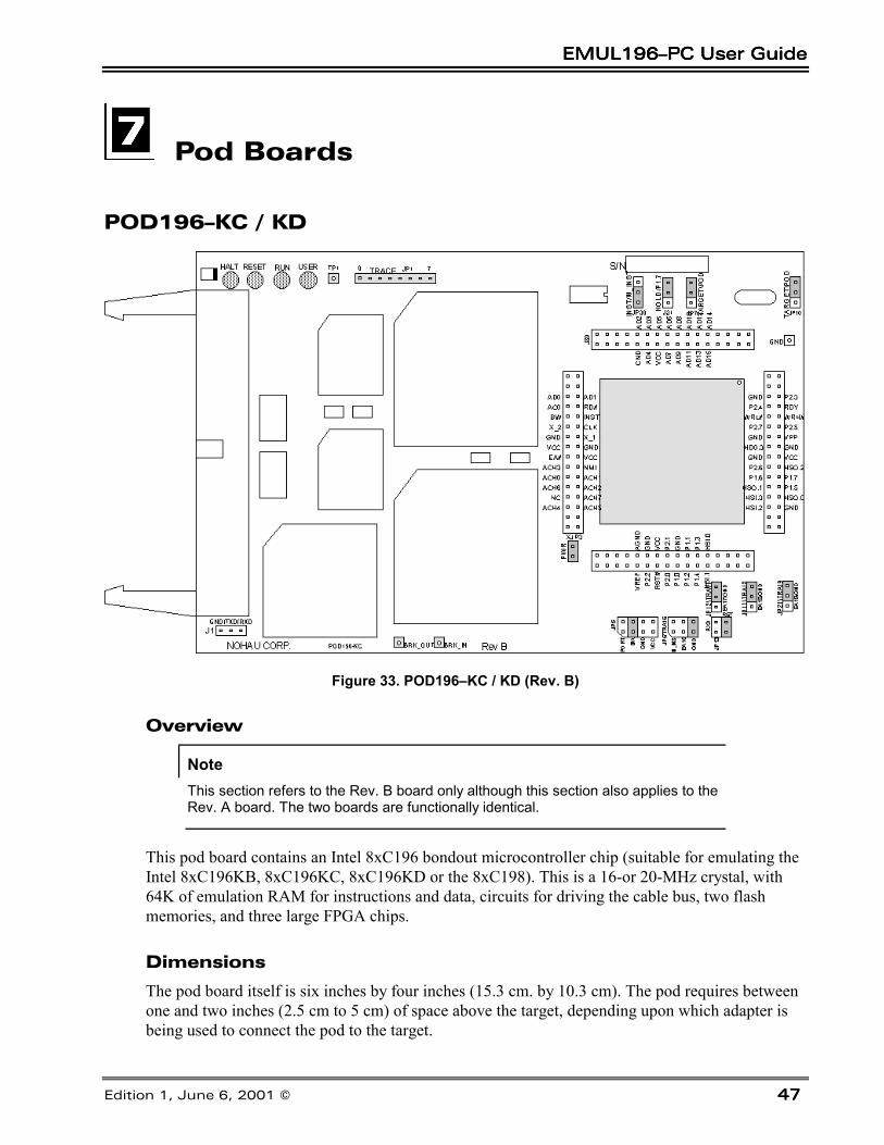
EMUL196–PC User GuideEMUL196–PC User GuideEMUL196–PC User GuideEMUL196–PC User Guide
Edition 1, June 6, 2001 © 474747
Pod Boards
POD196–KC / KD
Figure 33. POD196–KC / KD (Rev. B)
Overview
NoteThis section refers to the Rev. B board only although this section also applies to theRev. A board. The two boards are functionally identical.
This pod board contains an Intel 8xC196 bondout microcontroller chip (suitable for emulating theIntel 8xC196KB, 8xC196KC, 8xC196KD or the 8xC198). This is a 16-or 20-MHz crystal, with64K of emulation RAM for instructions and data, circuits for driving the cable bus, two flashmemories, and three large FPGA chips.
Dimensions
The pod board itself is six inches by four inches (15.3 cm. by 10.3 cm). The pod requires betweenone and two inches (2.5 cm to 5 cm) of space above the target, depending upon which adapter isbeing used to connect the pod to the target.
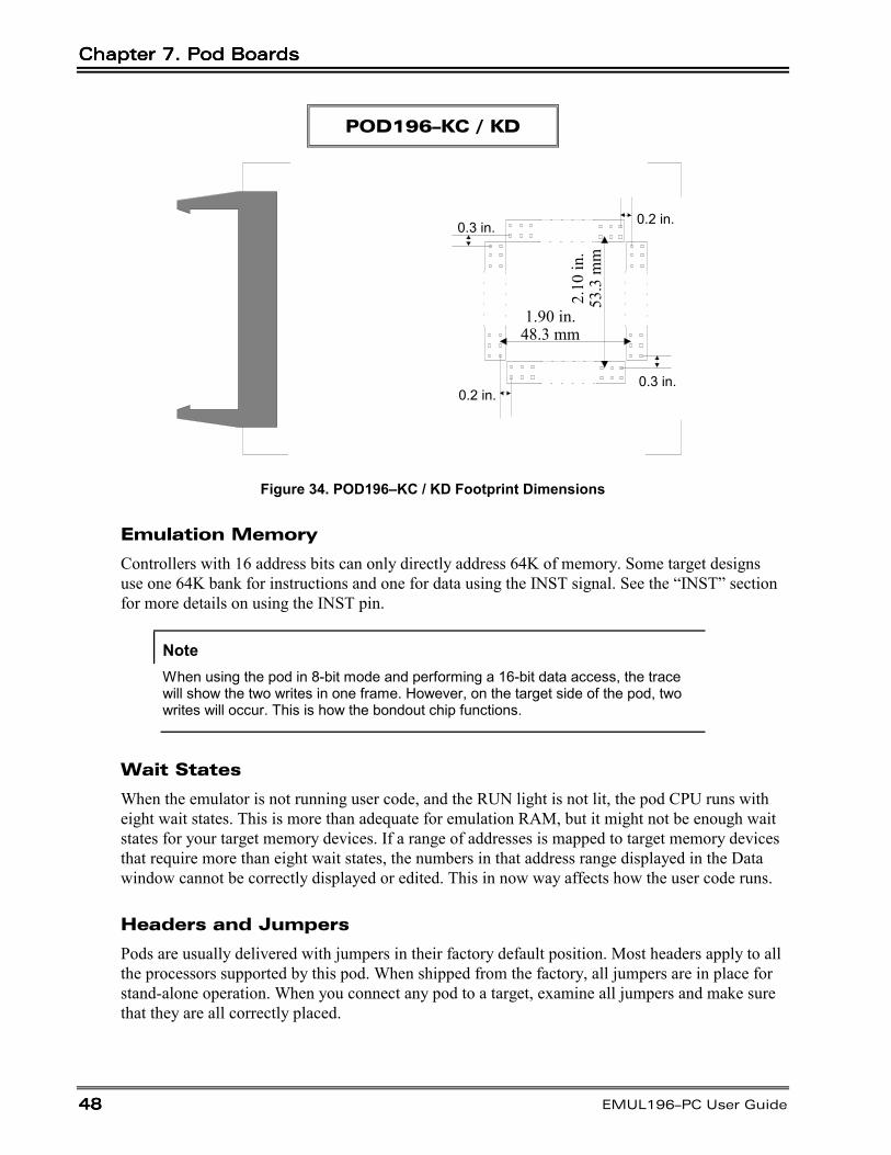
Chapter 7. Pod BoardsChapter 7. Pod BoardsChapter 7. Pod BoardsChapter 7. Pod Boards
48484848 EMUL196–PC User Guide
POD196–KC / KD
0.3 in. 0.2 in.
0.2 in.0.3 in.
1.90 in.48.3 mm
2.10
in.
53.3
mm
Figure 34. POD196–KC / KD Footprint Dimensions
Emulation Memory
Controllers with 16 address bits can only directly address 64K of memory. Some target designsuse one 64K bank for instructions and one for data using the INST signal. See the “INST” sectionfor more details on using the INST pin.
NoteWhen using the pod in 8-bit mode and performing a 16-bit data access, the tracewill show the two writes in one frame. However, on the target side of the pod, twowrites will occur. This is how the bondout chip functions.
Wait States
When the emulator is not running user code, and the RUN light is not lit, the pod CPU runs witheight wait states. This is more than adequate for emulation RAM, but it might not be enough waitstates for your target memory devices. If a range of addresses is mapped to target memory devicesthat require more than eight wait states, the numbers in that address range displayed in the Datawindow cannot be correctly displayed or edited. This in now way affects how the user code runs.
Headers and Jumpers
Pods are usually delivered with jumpers in their factory default position. Most headers apply to allthe processors supported by this pod. When shipped from the factory, all jumpers are in place forstand-alone operation. When you connect any pod to a target, examine all jumpers and make surethat they are all correctly placed.
EMUL196–PC User GuideEMUL196–PC User GuideEMUL196–PC User GuideEMUL196–PC User Guide
Edition 1, June 6, 2001 © 494949
POD196–KC / KD
ClockClockClockClock
These two headers each have two jumper positions: TARGET and POD. When set in theTARGET position, the pod controller receives the clock signal from the target crystal. Withboth in the POD position, the controller uses the crystal on the pod.
In ONCE mode, (only while using a clip-over adapter), all the target controller pins are tri-statedexcept the oscillator pins. Because there is no way to disconnect the target crystal from the targetcontroller, the target crystal remains an active part of the clock circuit even when the jumpers aremoved to the POD position. Where the two oscillators are running at the same frequency, theysynchronize naturally. The presence of two oscillators does not affect how the application runs. Ifthey are different frequencies, you probably want to put both jumpers in the TARGET position anduse just the target oscillator.
NoteWhen these jumpers are in the POD position, the XTAL signals on the pod aredisconnected from the target.
PWRPWRPWRPWR
Remove this jumper when the target has its own power supply. When this jumper is in place, thetarget can get Vcc from the pod as long as the current requirement is less than 0.5 amps. Highercurrents cause a significant voltage drop along the current path and the pod can be damaged.
NoteThe pod is specified to run at a nominal 5V +/- 5%, or from 4.75V to 5.25V. Atvoltages less than 4.70V, and at frequencies greater than 16 MHz, interruptsthat occur near the falling edge of CLOCKOUT might not be recognized. If youhave removed the PWR jumper and are using an external power supply, be surethe supply provides power within 5 percent of 5V.
RXD/TXD/GNDRXD/TXD/GNDRXD/TXD/GNDRXD/TXD/GND
On all of the 196 pods except POD196–EA, there are three pins labeled RXD/TXD/GND. Thisallows receive (RXD), transmit (TXD), and ground (GND) signals for the 196 processor.
If your target outputs debugging information on the serial port, you might want to connect anRS232 device like a terminal or a PC. The terminal is connected via clips or wires from these pinsto the terminal (input, output, and ground).
Chapter 7. Pod BoardsChapter 7. Pod BoardsChapter 7. Pod BoardsChapter 7. Pod Boards
50505050 EMUL196–PC User Guide
POD196–KC / KD
This pod includes a MAX232 chip to convert the signal levels from RS232 to TTL levels. Whetheror not you connect the RXD on J1 to an RS232 device, the MAX232 chip will drivethe serial port input pin on the controller. However, if P2.1 is used for low speed I/O, then JP13should be removed. To allow the MAX232 chip to drive the serial port input pin, place a jumperon this header.
The TXD pin gives the user the option of transmitting signals (output) to a terminal and a targetsimultaneously. The RXD signal on the other hand can only receive a signal (input) from onesource at a time. The following diagram shows how this functions.
Figure 35. Data Flow To and From the Target and the MAX232 Chip
The processor cannot handle input from two different sources at the same time. If you are con-nected to a terminal, through the MAX232 chip you must be in stand-alone mode (not connectedto a target). If you are connected to a target the RXD jumper on JP13 must be removed, so you arenot connected to a terminal and a target at the same time.
RSTRSTRSTRST
Occasionally, a target might contain an external device designed to reset the controller by pullingthe /RST pin low (i.e., a watchdog timer). The signal from the target /RST pin passes throughthe RST header. Removing the RST jumper prevents the external device from resetting the podcontroller.
HOLD: P1.7HOLD: P1.7HOLD: P1.7HOLD: P1.7
This jumper is factory installed in the P1.7 position, which is appropriate when this pin is used forlow speed I/O. If you plan to use this pin for carrying the HOLD signal, move this jumper to theHOLD position. With the jumper in the HOLD position, logic on the pod will prevent the HOLDsignal from reaching the controller while the emulator has control. When running the application,the HOLD signal will be passed through normally.
EMUL196–PC User GuideEMUL196–PC User GuideEMUL196–PC User GuideEMUL196–PC User Guide
Edition 1, June 6, 2001 © 515151
POD196–KC / KD
BUSWIDTH: JP5BUSWIDTH: JP5BUSWIDTH: JP5BUSWIDTH: JP5
From the factory, this header comes with a jumper installed in the BW position and, should neverneed to be removed. If your target uses only 16-bit wide bus, you can put an additional jumper inthe Vcc position. If your target only uses an 8-bit bus, you can put an additional jumper in theGND position. In a similar manner, the BW pin can be pulled high by placing two jumpers on theBUSWIDTH header: one on the BW pins and one of the Vcc pins. For more information about theBW pin on the 8xC196, refer to the Intel user manual for your controller type.
NoteThe pair of pins with the PORT label is reserved for a feature not yet implemented.Do not place a jumper on this pair of pins.
WARNING
Whether you pull the BW pin high or low, make sure that the jumper settings agree with yourtarget hardware design. If they are different, you can damage the pod, the target, or both. It isrecommended that you leave the Vcc and GND jumpers off when you are plugged into the target.This will allow the target to control the BW pin.
EA16-EA19EA16-EA19EA16-EA19EA16-EA19
The jumpers on these headers must remain in their default or grounded positions for all control-lers. If you use bank switching to address more than 64K, contact Nohau Technical Support([email protected]).
INSTINSTINSTINST
This section is intended for customers using the POD196–64 KC/KD who require more than 64Kaddress space. The pod was designed to handle this by using INST pin to access either code ordata by having 2x64K of emulation RAM and special jumpers which, can be used to access an ad-ditional 128K of memory. The emulator writes the data in the first 64K pages of memory and thecode in the second 64K pages in memory. New features have been added which allows support fora common bank and separate mapping of CODE and DATA. The trace currently cannot distin-guish between code and data symbols.
Chapter 7. Pod BoardsChapter 7. Pod BoardsChapter 7. Pod BoardsChapter 7. Pod Boards
52525252 EMUL196–PC User Guide
POD196–KC / KD
JP30: INST/M_INST (Two-Position)JP30: INST/M_INST (Two-Position)JP30: INST/M_INST (Two-Position)JP30: INST/M_INST (Two-Position)
This jumper passes the INST signal from the bondout chip to the target or passes the M_INST(gated INST) signal to the target. Leave this jumper in the default position. Normally you would toload your code into the emulator RAM and execute from this RAM instead of the target ROM.You will only need to move the JP30 jumper to the M_INST position when you have the podhooked to a target (mapped to target). You can view this code ROM in the Program window.
If you move the JP30 jumper to the M_INST location, note that the hardware on the pod will gatethe INST pin with a delay of 10 ns. This will cause it to be held high when you access the commoncode/data bank.
JP6: M_INST – EA16-GND (Three-Position)JP6: M_INST – EA16-GND (Three-Position)JP6: M_INST – EA16-GND (Three-Position)JP6: M_INST – EA16-GND (Three-Position)
This jumper controls what the emulation RAM and the trace board sees on signal A16. Place thisjumper in the GND position for normal <64K mode. Place this jumper in the M_INST position for>64K mode.
WARNING
Never place this jumper in the EA16 position with a KC pod (EA16 is a non-connect pin intended forbank switching, which is not supported).
The M_INST signal is generated by the logic on the pod and is either:
• Always high when accessing the code area or common code/data bank,
OR
• Is equal to the CPU INST signal.
This signal allows the emulator to view code in the Source window or data in the Data window.
All hardware breakpoints will effect code space only.
EMUL196–PC User GuideEMUL196–PC User GuideEMUL196–PC User GuideEMUL196–PC User Guide
Edition 1, June 6, 2001 © 535353
POD196–KC / KD
Procedure to Test
1. Place jumpers JP6 in the M_INST location
2. Start the emulator
3. Click Reset
4. Make sure PC = 2080H and SP = 200H
5. Click in the Source window
6. Type in this program at 2080H:NOPINC 1CST 1C, 2080LJMP 2080
7. Click Go
8. Click Break
9. View the Source window and Data window to verify that you can look at data at 2080H andcode at 2080H.
10. All hardware breakpoints will be placed in the code bank.
Some users only want to have the INST pin supported from 8000 – FFFF. The emulator uses theINST pin to make 2x64K bank available. You can get around this by putting code tables for dataaccess below 8000 in both the code bank and in the data bank in the on pod emulation RAM.
Memory Mapping
The memory map menu in the windows software will let you map code and data individuallyto your target when you use the INST pin. For mapping data, use the address range as usual(0000 – FFFF). For mapping code, use the address range ORd with 10000H (12080H – 13000Hwill map code between address 2080H – 3000H to target).
Chapter 7. Pod BoardsChapter 7. Pod BoardsChapter 7. Pod BoardsChapter 7. Pod Boards
54545454 EMUL196–PC User Guide
POD196–KC / KD
Hardware Breakpoint Setup
The hardware breakpoint setup window allows you to set a hardware breakpoint when running outof a target ROM. To do so, use the address range ORd with 10000H (to set a hardware breakpointat address 2090H in your code ROM, enter address 12090H in the setup menu).
NoteThe JP30 jumper is also available for the KR/NT pod, but is implemented as asurface mounted resistor jumper named RJP6. This jumper must be moved tolocation 2–3 to get the gated INST line connected to the target. The software doesnot support separate code and data mapping or the INST mask for the KR/NT pod.
Helpful Hints for Compiling
Use the following linker invocation where you have overlapping ROMs decoded by the INST pin,one for CONST segment and one for CODE segment:
rl196 cstart.obj, hello.obj, c96.lib to hello.omf &md(kc) romdata(02000h-03fffh) &romcode (02000h-03fffh) &inst
This will normally generate code for two separate ROMs, both at address 2000h-03fffh with theINST pin on the target selecting either one. (In the omf file one is a CONST segment and the othera CODE segment, both at the same address.) Load the code into the emulator twice, switching theINST jumpers each time to load into both code and data spaces. Start with the jumper in the INSTposition and end with the jumper in the M_INST position. This will fail because each time, as theCODE segment is loaded into both the code and data spaces. The CONST segment from the .omffile will never be loaded into data space no matter what you do.
The only work around is to use the OH196 object hex utility to generate a hex file, which extractsonly CONST segments to put into the data space. Using the above example, the invocation wouldbe as follows:oh196 –o romdata.hex –s const hello.omf
Then, romdata.hex is loaded into the data space by selecting INST jumper settings and hello.omfis loaded into the code space by selecting M_INST jumper settings. This has now loaded the cor-rect code/data into both code and data spaces. A limitation (apart from having to remember to loadtwo separate files using two different sets of jumper settings each time) is that you will not haveaccess to symbolic debugging of any CONST segments that overlap CODE segments.
EMUL196–PC User GuideEMUL196–PC User GuideEMUL196–PC User GuideEMUL196–PC User Guide
Edition 1, June 6, 2001 © 555555
POD196–KC / KD
Download Procedure
Following is the procedure to download a common code/data bank residing between 0 – 7FFF andthe rest of the code.
1. Move JP6 to GND and JP30 to INST position to load code constants to your data bank.
2. Download your code table (0 – 7FFF).
3. Move JP6 and JP30 to M_INST position to load code to your code bank
4. Download your code table (0 – 7FFF) again.
5. Download your code from 8000 – FFFF.
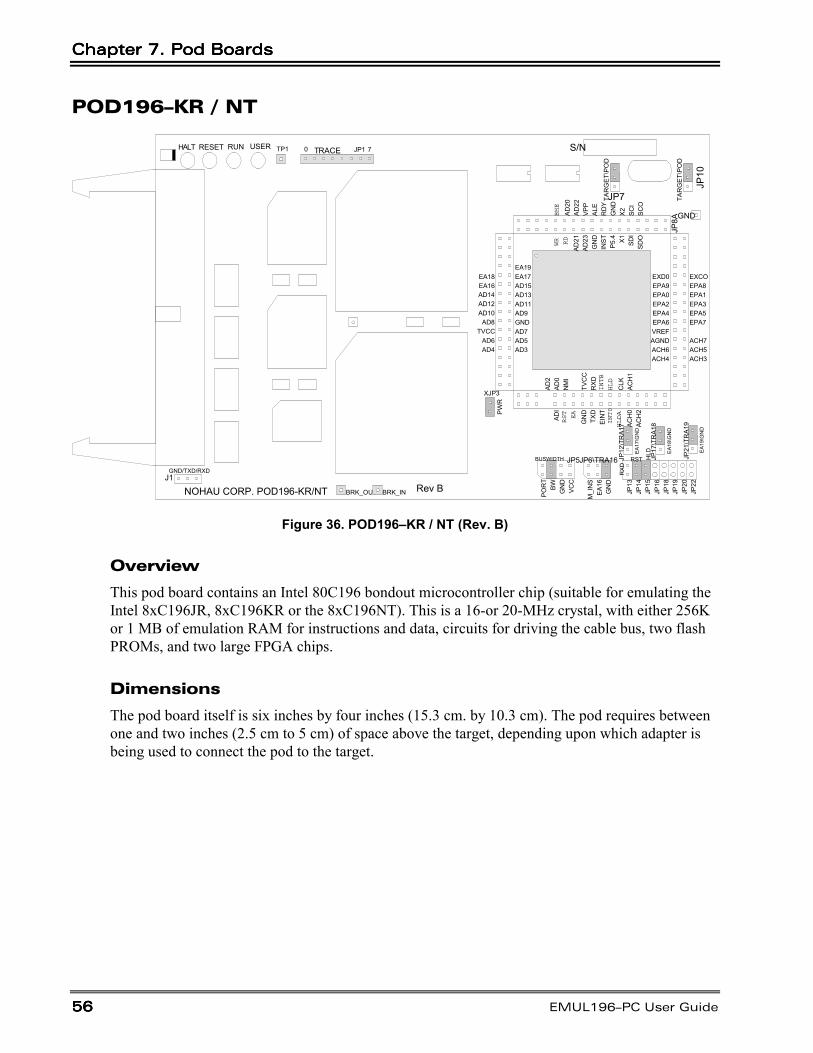
Chapter 7. Pod BoardsChapter 7. Pod BoardsChapter 7. Pod BoardsChapter 7. Pod Boards
56565656 EMUL196–PC User Guide
POD196–KR / NT
NOHAU CORP. POD196-KR/NT
TP1
TAR
GET
\PO
D
JP10
XJP3
PWR
TRACE JP1 S/N
J1
EA19EA17AD15AD13AD11AD9GNDAD7AD5AD3
EA18EA16AD14AD12AD10
AD8TVCC
AD6AD4
AD2
AD0
NM
I
TVC
CR
XDINTB
HLD
CLK
ACH
1
ADI
RST
EA
GN
DTX
DEI
NT
INT0
HLDA
ACH
0AC
H2
JP7
BHE
AD20
AD22
VPP
ALE
RD
YG
ND
X2 SCI
SCO
WR RD
AD21
AD23
GN
DIN
STP5
.4 X1 SDI
SDO
GND
JP8A
JP13
JP14
JP15
JP16
JP18
JP19
JP20
JP22
M_I
NS
EA16
GN
D
POR
TBW GN
DVC
C
EA17
\GN
D
EA18
\GN
D
EA19
\GN
D
RST HLD
EXD0EPA9EPA0EPA2EPA4EPA6VREFAGNDACH6ACH4
EXCOEPA8EPA1EPA3EPA5EPA7
ACH7ACH5ACH3
TAR
GET
\PO
D
Rev B
HALT RESET RUN USER 70
GND/TXD/RXD
JP5JP6\TRA16 JP12
\TR
A17
JP17
\TR
A18
JP21
\TR
A19
BUSWIDTH
RXD
BRK_OUT BRK_IN
Figure 36. POD196–KR / NT (Rev. B)
Overview
This pod board contains an Intel 80C196 bondout microcontroller chip (suitable for emulating theIntel 8xC196JR, 8xC196KR or the 8xC196NT). This is a 16-or 20-MHz crystal, with either 256Kor 1 MB of emulation RAM for instructions and data, circuits for driving the cable bus, two flashPROMs, and two large FPGA chips.
Dimensions
The pod board itself is six inches by four inches (15.3 cm. by 10.3 cm). The pod requires betweenone and two inches (2.5 cm to 5 cm) of space above the target, depending upon which adapter isbeing used to connect the pod to the target.
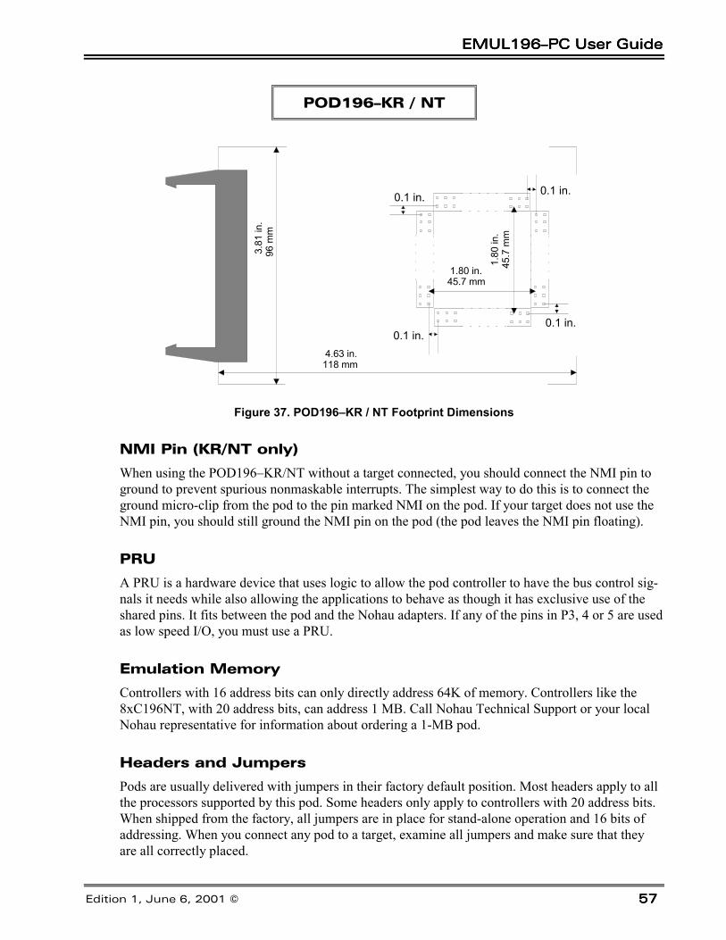
EMUL196–PC User GuideEMUL196–PC User GuideEMUL196–PC User GuideEMUL196–PC User Guide
Edition 1, June 6, 2001 © 575757
POD196–KR / NT
0.1 in. 0.1 in.
0.1 in.0.1 in.
1.8
0 in
.45
.7 m
m
1.80 in.45.7 mm
3.8
1 in
.96
mm
4.63 in.118 mm
Figure 37. POD196–KR / NT Footprint Dimensions
NMI Pin (KR/NT only)
When using the POD196–KR/NT without a target connected, you should connect the NMI pin toground to prevent spurious nonmaskable interrupts. The simplest way to do this is to connect theground micro-clip from the pod to the pin marked NMI on the pod. If your target does not use theNMI pin, you should still ground the NMI pin on the pod (the pod leaves the NMI pin floating).
PRU
A PRU is a hardware device that uses logic to allow the pod controller to have the bus control sig-nals it needs while also allowing the applications to behave as though it has exclusive use of theshared pins. It fits between the pod and the Nohau adapters. If any of the pins in P3, 4 or 5 are usedas low speed I/O, you must use a PRU.
Emulation Memory
Controllers with 16 address bits can only directly address 64K of memory. Controllers like the8xC196NT, with 20 address bits, can address 1 MB. Call Nohau Technical Support or your localNohau representative for information about ordering a 1-MB pod.
Headers and Jumpers
Pods are usually delivered with jumpers in their factory default position. Most headers apply to allthe processors supported by this pod. Some headers only apply to controllers with 20 address bits.When shipped from the factory, all jumpers are in place for stand-alone operation and 16 bits ofaddressing. When you connect any pod to a target, examine all jumpers and make sure that theyare all correctly placed.
Chapter 7. Pod BoardsChapter 7. Pod BoardsChapter 7. Pod BoardsChapter 7. Pod Boards
58585858 EMUL196–PC User Guide
POD196–KR / NT
ClockClockClockClock
These two headers each have two jumper positions: TARGET and POD. When set in theTARGET position, the pod controller receives the clock signal from the target crystal. Withboth in the POD position, the controller uses the crystal on the pod.
NoteWhen the clock jumpers are in the pod position, the XTAL signals from the pod aredisconnected from the target.
In ONCE mode, (only while using a clip-over adapter), all the target controller pins are tri-statedexcept the oscillator pins. Because there is no way to disconnect the target crystal from the targetcontroller, the target crystal remains an active part of the clock circuit even when the jumpers aremoved to the POD position. Where the two oscillators are running at the same frequency, theysynchronize naturally. The presence of two oscillators does not affect how the application runs. Ifthey are different frequencies, you probably want to put both jumpers in the TARGET position anduse just the target oscillator.
PWRPWRPWRPWR
Remove this jumper when the target has its own power supply. When this jumper is in place, thetarget can get Vcc from the pod as long as the current requirement is less than 0.5 amps. Highercurrents cause a significant voltage drop along the current path and the pod can be damaged.
NoteThe pod is specified to run at a nominal 5V +/- 5%, or from 4.75V to 5.25V. At volt-ages less than 4.70V, and at frequencies greater than 16 MHz, interrupts that occurnear the falling edge of CLOCKOUT might not be recognized. If you have removedthe PWR jumper and are using an external power supply, be sure the supply pro-vides power within 5 percent of 5V.
RXD/TXD/GNDRXD/TXD/GNDRXD/TXD/GNDRXD/TXD/GND
On all of the 196 pods except POD196–EA, there are three pins labeled RXD/TXD/GND. Thisallows receive (RXD), transmit (TXD), and ground (GND) signals for the 196 processor. If yourtarget outputs debugging information on the serial port, you might want to connect an RS232 de-vice like a terminal or a PC. The terminal is connected via clips or wires from these pins to theterminal (input, output, and ground).
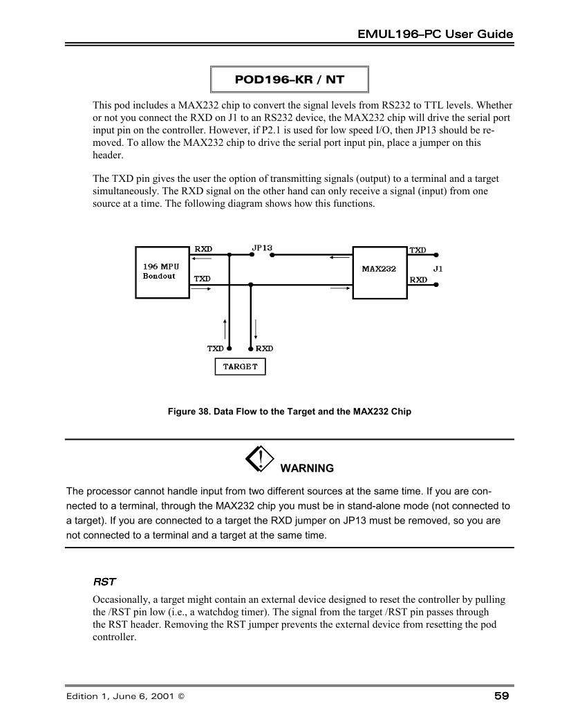
EMUL196–PC User GuideEMUL196–PC User GuideEMUL196–PC User GuideEMUL196–PC User Guide
Edition 1, June 6, 2001 © 595959
POD196–KR / NT
This pod includes a MAX232 chip to convert the signal levels from RS232 to TTL levels. Whetheror not you connect the RXD on J1 to an RS232 device, the MAX232 chip will drive the serial portinput pin on the controller. However, if P2.1 is used for low speed I/O, then JP13 should be re-moved. To allow the MAX232 chip to drive the serial port input pin, place a jumper on thisheader.
The TXD pin gives the user the option of transmitting signals (output) to a terminal and a targetsimultaneously. The RXD signal on the other hand can only receive a signal (input) from onesource at a time. The following diagram shows how this functions.
Figure 38. Data Flow to the Target and the MAX232 Chip
WARNING
The processor cannot handle input from two different sources at the same time. If you are con-nected to a terminal, through the MAX232 chip you must be in stand-alone mode (not connected toa target). If you are connected to a target the RXD jumper on JP13 must be removed, so you arenot connected to a terminal and a target at the same time.
RSTRSTRSTRST
Occasionally, a target might contain an external device designed to reset the controller by pullingthe /RST pin low (i.e., a watchdog timer). The signal from the target /RST pin passes throughthe RST header. Removing the RST jumper prevents the external device from resetting the podcontroller.
Chapter 7. Pod BoardsChapter 7. Pod BoardsChapter 7. Pod BoardsChapter 7. Pod Boards
60606060 EMUL196–PC User Guide
POD196–KR / NT
HLDHLDHLDHLD
The target HLD signal passes through the HLD header. Removing this jumper will prevent the podcontroller from receiving the Hold Request from a target device.
BUSWIDTHBUSWIDTHBUSWIDTHBUSWIDTH
This header controls the signal sent to the FLEX logic chips. The bondout chip does not correctlyassert the bus control signals when the CCBs are set to have an 8-bit wide bus. If you need toemulate an 8-bit bus, you can do so reliably by setting the CCBs to have a dynamic buswidth andadding a jumper to this header in the GND position. Have two jumpers on this header, one in theBW position and one in the GND position.
NoteThe pair of pins on the BUSWIDTH header with the PORT label is reserved for afeature not yet implemented. Do not place the jumper on this pair of pins.
WARNING
Whether you pull the BW pin high or low, make sure that the jumper settings agree with your targethardware design. If they are different, you can damage the pod, the target, or both. Do not insert ajumper on both the Vcc and GND when you are plugged into the target. This will allow the target tocontrol the BW pin.
EA16-EA19EA16-EA19EA16-EA19EA16-EA19
The jumpers on these headers must remain in their default or grounded positions for all controllersthat use 16 address bits. Controllers like the 8xC196NT have 20 address bits and will likely needto change these jumpers.
Each of these jumpers sits between the controller and the address signals going to the emulator andtrace boards. These address signals are used to correctly locate write cycles in Shadow RAM andtrace records of all kinds in the trace buffer.
If your application uses a controller with 20 address bits, for every address bit above 15 that theapplication uses for addressing, move the corresponding jumper from the GND position to theEA1x position. This will pass that address signal on to the emulator and trace boards. For each ofthe bits that are used for I/O instead of addressing, put the jumper on the GND side. This applies toJP/TRA16 although it has a different geometry than the other headers.
EMUL196–PC User GuideEMUL196–PC User GuideEMUL196–PC User GuideEMUL196–PC User Guide
Edition 1, June 6, 2001 © 616161
POD196–KR / NT
WARNING
Do not put more than one jumper on EA16, also labeled JP6. Having two jumpers on this headercan damage the bondout controller or some other part of the pod.
KR/NT Ready Functionality
The KR/NT pod uses a bondout version of the 196NT. When designing this chip, Intel remappedthe P5 SFRs to external memory. This makes them inaccessible and P5.6 cannot be configured asthe READY input signal.
Programming the CCBs for infinite Wait States automatically enables P5.6 to function as theREADY input and it will control the duration of the Wait State. However, when the CCBs areprogrammed for any other number of Wait States, the internal ready circuitry always reads a zeroand Wait States are inserted as specified by the CCBs. Because P5.6 cannot be configured as theREADY input, holding P5.6 high will not cancel the Wait States.
SolutionSolutionSolutionSolution
To regain READY functionality, a wire jumper should be placed on the pod from the READY pinto TP16 (BRK_IN) at the edge of the pod. The rest is taken care of by the new bin files (*.bin) onthe CD-ROM disk accompanying the pod board.
NoteThis solution takes over the use of BRK_IN (TP16). If the BRK_IN function isneeded, this solution cannot be used.
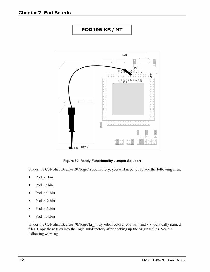
Chapter 7. Pod BoardsChapter 7. Pod BoardsChapter 7. Pod BoardsChapter 7. Pod Boards
62626262 EMUL196–PC User Guide
POD196–KR / NT
S/N
JP7
BHE
AD20
AD22
VPP
ALE
RD
YG
ND
X2 SCI
SCO
WR RD
AD21
AD23
GN
DIN
STP5
.4 X1 SDI
SDO
JP8A
HLD
Rev BBRK_IN
Figure 39. Ready Functionality Jumper Solution
Under the C:\Nohau\Seehau196\logic\ subdirectory, you will need to replace the following files:
• Pod_kr.bin
• Pod_nt.bin
• Pod_nt1.bin
• Pod_nt2.bin
• Pod_nt3.bin
• Pod_nt4.bin
Under the C:\Nohau\Seehau196\logic\kr_ntrdy subdirectory, you will find six identically namedfiles. Copy these files into the logic subdirectory after backing up the original files. See thefollowing warning.
EMUL196–PC User GuideEMUL196–PC User GuideEMUL196–PC User GuideEMUL196–PC User Guide
Edition 1, June 6, 2001 © 636363
POD196–KR / NT
WARNING
The six original files should be copied to another subdirectory (you will need to create a separatesubdirectory first) and then replaced with the ones under the kr_ntrdy subdirectory. If the BRK_INfunction is needed later, the original files can be restored.
NoteThis modification will use P5.6 as READY regardless of how Port 5 is configured. IfP5.6 is intended to be used as READY, the user must remember to configure theport properly or the user code might work on the emulator, but fail in the final de-sign.
The software will restore the READY pin functionality for true emulation of 196KR/NT control-lers. The user should connect a jumper from TP16 to GND if P5.6 is to be used for I/O or fromTP16 to the READY pin if P5.6 is to be used as the READY input. When the jumper is connectedto the READY pin, P5.6 will always control wait states regardless of how Port 5 is configured.
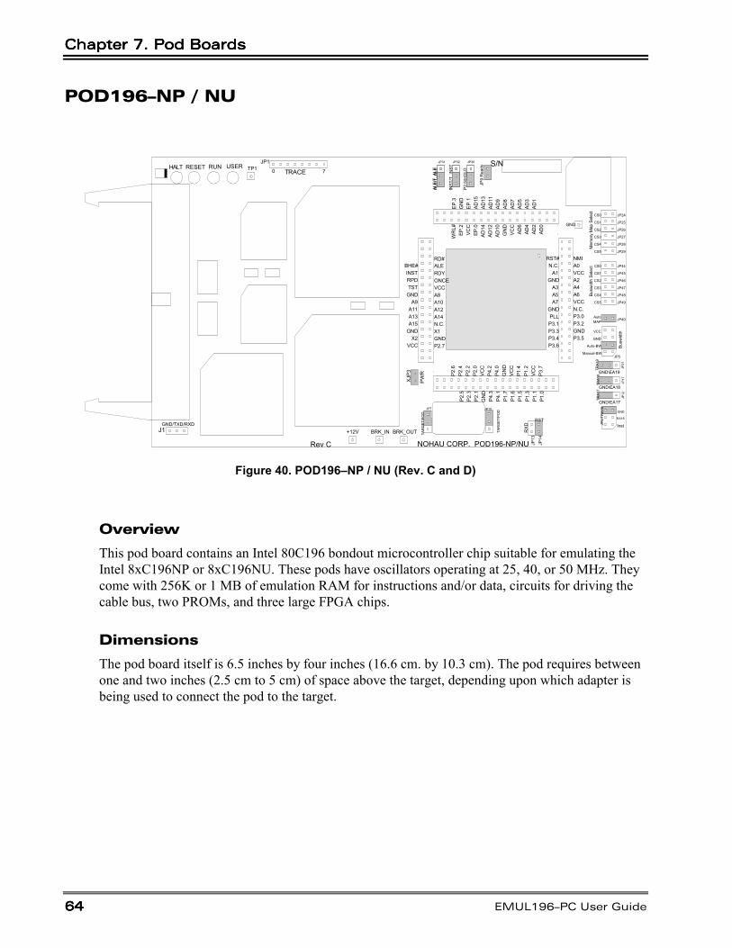
Chapter 7. Pod BoardsChapter 7. Pod BoardsChapter 7. Pod BoardsChapter 7. Pod Boards
64646464 EMUL196–PC User Guide
POD196–NP / NU
NOHAU CORP. POD196-NP/NU
TP1
TAR
GET
\PO
D
JP10
TRACE
JP1 S/N
J1
JP7
JP13
Inst
GND\EA18
GND\EA19
RST
TAR
GET
\PO
D
Rev C
HALT RESET RUN USER70
GND/TXD/RXD
TRA1
8
JP21
BRK_OUTBRK_IN
EA16
GNDXJ
P3
PW
R
RD#ALERDYONCEVCCA8A10A12A14N.C.X1GNDP2.7
P2.6
P2.4
P2.2
P2.0
VCC
P4.2
P4.0
GN
DVC
CP1
.4P1
.2VC
CP3
.7
P2.5
P2.3
P2.1
GN
DP4
.3P4
.1P1
.7P1
.6P1
.5P1
.3P1
.1P1
.0
EP.3
GN
DEP
.1AD
15AD
13AD
11AD
9AD
8AD
7AD
5AD
3AD
1
WR
L#EP
.2VC
CEP
.0AD
14AD
12AD
10G
ND
VCC
AD6
AD4
AD2
AD0 GND
RST#N.C.
A1GND
A3A5A7
GNDPLLP3.1P3.3P3.4P3.6
NMIA0VCCA2A4A6VCCN.C.P3.0P3.2GNDP3.5
BHE#INSTRPDTST
GNDA9
A11A13A15
GNDX2
VCC
JP14
P2.5
/HO
LD
INST
/T_I
NST
ALE/
T_AL
E
JP6/
TRA1
6
RXD
+12VAL
E/T_
ALE
JP5
Auto-BW
GND
VCC
Manual-BW
Busw
idth
TRA1
9
JP17
GND\EA17
TRA1
7
JP12
CS0
CS1
CS2
CS3
CS4
CS5
CS0
CS1
CS2
CS3
CS4
CS5
JP24
JP25
JP26
JP27
JP28
JP29
JP44
JP45
JP46
JP47
JP48
JP49
Busw
idth
Sel
ect
Mem
ory
Map
Sel
ect
JP9
Rea
dy
JP31 JP32 JP30
AutoMAP JP40
Figure 40. POD196–NP / NU (Rev. C and D)
Overview
This pod board contains an Intel 80C196 bondout microcontroller chip suitable for emulating theIntel 8xC196NP or 8xC196NU. These pods have oscillators operating at 25, 40, or 50 MHz. Theycome with 256K or 1 MB of emulation RAM for instructions and/or data, circuits for driving thecable bus, two PROMs, and three large FPGA chips.
Dimensions
The pod board itself is 6.5 inches by four inches (16.6 cm. by 10.3 cm). The pod requires betweenone and two inches (2.5 cm to 5 cm) of space above the target, depending upon which adapter isbeing used to connect the pod to the target.
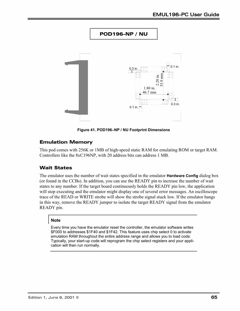
EMUL196–PC User GuideEMUL196–PC User GuideEMUL196–PC User GuideEMUL196–PC User Guide
Edition 1, June 6, 2001 © 656565
POD196–NP / NU
0.3 in. 0.1 in.
0.1 in.0.3 in.
1.80 in.46.7 mm
2.20
in.
55.9
mm
Figure 41. POD196–NP / NU Footprint Dimensions
Emulation Memory
This pod comes with 256K or 1MB of high-speed static RAM for emulating ROM or target RAM.Controllers like the 8xC196NP, with 20 address bits can address 1 MB.
Wait States
The emulator uses the number of wait states specified in the emulator Hardware Config dialog box(or found in the CCBs). In addition, you can use the READY pin to increase the number of waitstates to any number. If the target board continuously holds the READY pin low, the applicationwill stop executing and the emulator might display one of several error messages. An oscilloscopetrace of the READ or WRITE strobe will show the strobe signal stuck low. If the emulator hangsin this way, remove the READY jumper to isolate the target READY signal from the emulatorREADY pin.
NoteEvery time you have the emulator reset the controller, the emulator software writes$F000 to addresses $1F40 and $1F42. This feature uses chip select 0 to activateemulation RAM throughout the entire address range and allows you to load code.Typically, your start-up code will reprogram the chip select registers and your appli-cation will then run normally.
Chapter 7. Pod BoardsChapter 7. Pod BoardsChapter 7. Pod BoardsChapter 7. Pod Boards
66666666 EMUL196–PC User Guide
POD196–NP / NU
Headers and Jumpers
Pods are usually delivered with jumpers in their factory default position (stand-alone position).Some of the headers are quite close together and their labels can be hard to read. When you doconnect the pod to a target be sure to examine all jumpers and make sure that they are all correctlyplaced. Use the descriptions below as a guide to jumper placement.
ClockClockClockClock
These two headers are labeled JP7 and JP10. They each have two jumper positions: TARGETand POD. They must be moved as a pair. When set in the TARGET position, the pod controllerreceives the clock signal from the target crystal (oscillator). With both in the POD position, thecontroller uses the crystal on the pod.
NoteWhen the clock jumpers are in the POD position, the XTAL signals are completelydisconnected from the target.
PWRPWRPWRPWR
Remove this jumper when the target has its own power supply. When this jumper is in place, thetarget will get Vcc from the pod, which can supply up to 0.5 amps. Higher currents cause a signifi-cant voltage drop along the current path and the pod can be damaged.
RXD/TXD/GNDRXD/TXD/GNDRXD/TXD/GNDRXD/TXD/GND
On all of the 196 pods except POD196–EA, there are three pins labeled RXD/TXD/GND. Thisallows receive (RXD), transmit (TXD), and ground (GND) signals for the 196 processor.
If your target outputs debugging information on the serial port, you might want to connect anRS232 device like a terminal or a PC. The terminal is connected via clips or wires from these pinsto the terminal (input, output, and ground).
This pod includes a MAX232 chip to convert the signal levels from RS232 to TTL levels. Whetheror not you connect the RXD on J1 to an RS232 device, the MAX232 chip will drivethe serial port input pin on the controller. However, if P2.1 is used for low speed I/O, then JP13should be removed. To allow the MAX232 chip to drive the serial port input pin, place a jumperon this header.
The TXD pin gives the user the option of transmitting signals (output) to a terminal and a targetsimultaneously. The RXD signal on the other hand can only receive a signal (input) from onesource at a time. The following diagram shows how this functions.
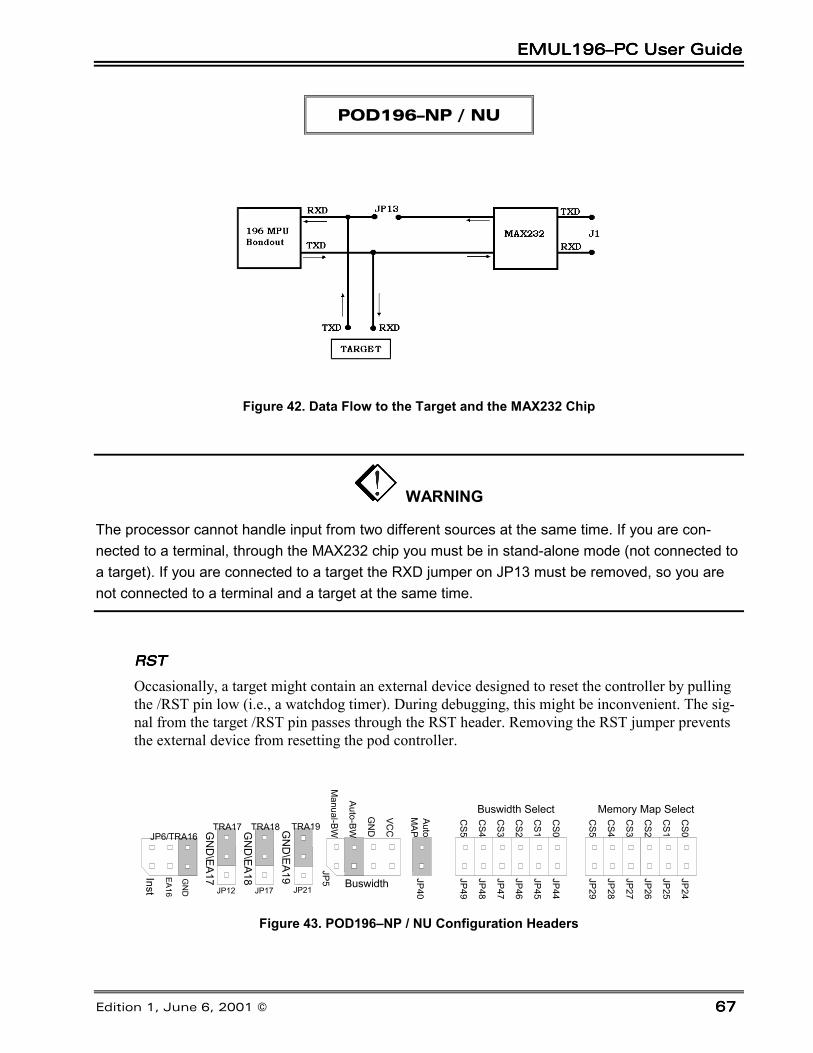
EMUL196–PC User GuideEMUL196–PC User GuideEMUL196–PC User GuideEMUL196–PC User Guide
Edition 1, June 6, 2001 © 676767
POD196–NP / NU
Figure 42. Data Flow to the Target and the MAX232 Chip
WARNING
The processor cannot handle input from two different sources at the same time. If you are con-nected to a terminal, through the MAX232 chip you must be in stand-alone mode (not connected toa target). If you are connected to a target the RXD jumper on JP13 must be removed, so you arenot connected to a terminal and a target at the same time.
RSTRSTRSTRST
Occasionally, a target might contain an external device designed to reset the controller by pullingthe /RST pin low (i.e., a watchdog timer). During debugging, this might be inconvenient. The sig-nal from the target /RST pin passes through the RST header. Removing the RST jumper preventsthe external device from resetting the pod controller.
Inst
GN
D\EA18
GN
D\EA19
TRA18
JP21
EA16
GN
D
JP6/TRA16
JP5
Auto-BW
GN
D
VCC
Manual-BW
Buswidth
TRA19
JP17
GN
D\EA17
TRA17
JP12
CS0
CS1
CS2
CS3
CS4
CS5
CS0
CS1
CS2
CS3
CS4
CS5
JP24
JP25
JP26
JP27
JP28
JP29
JP44
JP45
JP46
JP47
JP48
JP49
Buswidth Select Memory Map SelectAutoM
APJP40
Figure 43. POD196–NP / NU Configuration Headers
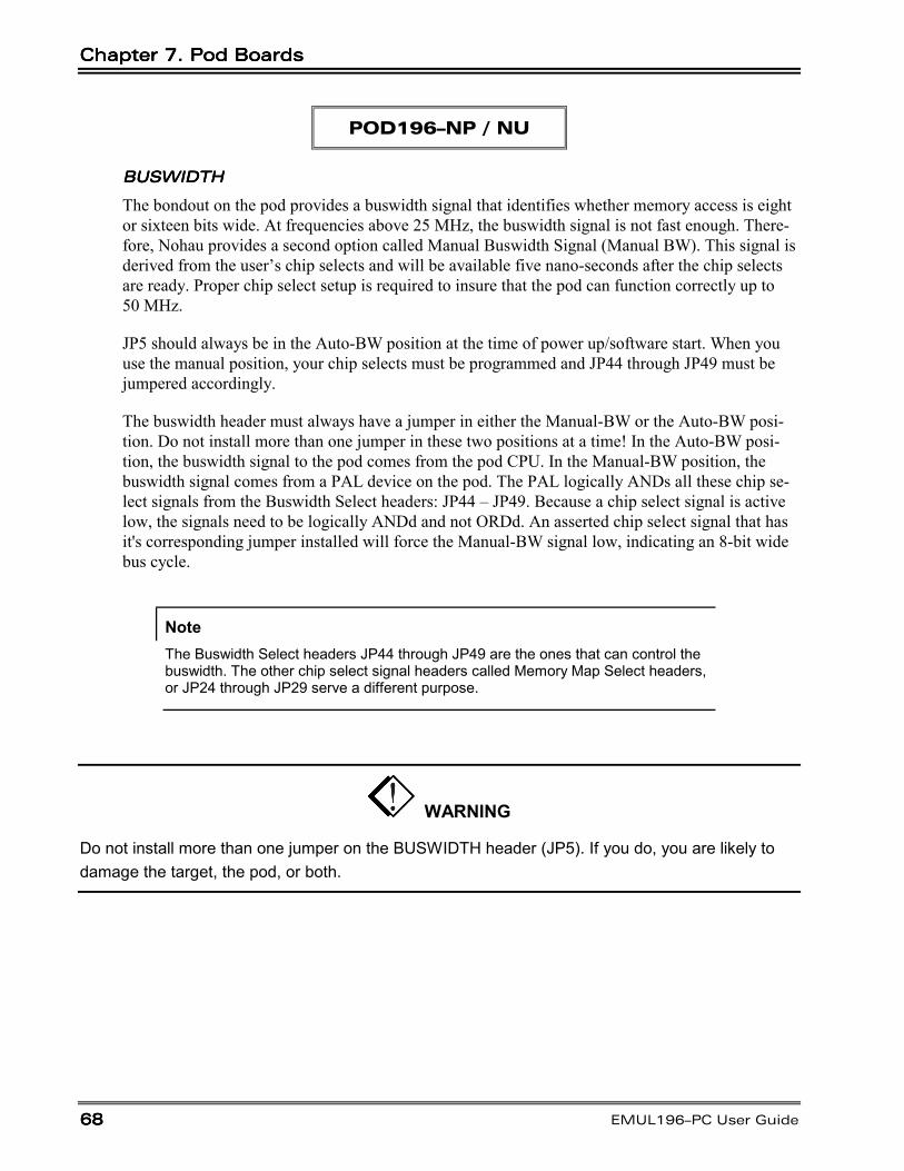
Chapter 7. Pod BoardsChapter 7. Pod BoardsChapter 7. Pod BoardsChapter 7. Pod Boards
68686868 EMUL196–PC User Guide
POD196–NP / NU
BUSWIDTHBUSWIDTHBUSWIDTHBUSWIDTH
The bondout on the pod provides a buswidth signal that identifies whether memory access is eightor sixteen bits wide. At frequencies above 25 MHz, the buswidth signal is not fast enough. There-fore, Nohau provides a second option called Manual Buswidth Signal (Manual BW). This signal isderived from the user’s chip selects and will be available five nano-seconds after the chip selectsare ready. Proper chip select setup is required to insure that the pod can function correctly up to50 MHz.
JP5 should always be in the Auto-BW position at the time of power up/software start. When youuse the manual position, your chip selects must be programmed and JP44 through JP49 must bejumpered accordingly.
The buswidth header must always have a jumper in either the Manual-BW or the Auto-BW posi-tion. Do not install more than one jumper in these two positions at a time! In the Auto-BW posi-tion, the buswidth signal to the pod comes from the pod CPU. In the Manual-BW position, thebuswidth signal comes from a PAL device on the pod. The PAL logically ANDs all these chip se-lect signals from the Buswidth Select headers: JP44 – JP49. Because a chip select signal is activelow, the signals need to be logically ANDd and not ORDd. An asserted chip select signal that hasit's corresponding jumper installed will force the Manual-BW signal low, indicating an 8-bit widebus cycle.
NoteThe Buswidth Select headers JP44 through JP49 are the ones that can control thebuswidth. The other chip select signal headers called Memory Map Select headers,or JP24 through JP29 serve a different purpose.
WARNING
Do not install more than one jumper on the BUSWIDTH header (JP5). If you do, you are likely todamage the target, the pod, or both.
EMUL196–PC User GuideEMUL196–PC User GuideEMUL196–PC User GuideEMUL196–PC User Guide
Edition 1, June 6, 2001 © 696969
POD196–NP / NU
Buswidth SelectBuswidth SelectBuswidth SelectBuswidth Select
All the chip select signals are brought to their respective headers so they can be used to control theManual-BW signal. This is necessary if you are running your target at speeds higher than 25 MHz.At these high speeds, the Manual-BW logic will make sure that the buswidth signal will arriveearly, reducing noise. If the Auto-BW signal is used at these high speeds, your target can latch thewrong address due to noise.
NoteIf you have the jumpers set to use a Manual-BW signal the very first time you startup the emulator hardware and software, you must have a jumper on header JP44.If you do not, you will see unwanted breakpoints. You only need to have this jumperthere the first time you power up the emulator. After that, it can be removed.
Another way to avoid these breakpoints is to:
1. Select the Hardware Breakpoint menu
2. Add a temporary breakpoint
3. Click OK
4. Go back to the Hardware Breakpoint menu
5. Remove the temporary breakpoint.
If you have a jumper on the AutoMap header (JP40):
1. Open the Memory Map dialog box
2. Set a temporary mapping
3. Click OK.
4. Remove it.
AutoMap HeaderAutoMap HeaderAutoMap HeaderAutoMap Header
Memory can be mapped either with a software setting or by using chip select signals. Removingthe jumper on this header (JP40) will ensure that the software memory mapping signal does notreach the mapping logic.
Chapter 7. Pod BoardsChapter 7. Pod BoardsChapter 7. Pod BoardsChapter 7. Pod Boards
70707070 EMUL196–PC User Guide
POD196–NP / NU
EA16-EA19EA16-EA19EA16-EA19EA16-EA19
Each of these jumpers sits between the controller and the address signals going to the emulator andtrace boards. These address signals are used to correctly address emulation RAM on the pod, lo-cate write cycles in Shadow RAM and assign addresses to trace records in the trace buffer.
If your application uses more than 16 address bits, for every address bit above 15 that the applica-tion uses for addressing, move the corresponding jumper from the GND position to the EA1x po-sition. This will pass that address signal on to the emulator and trace boards. For each of the bitsthat are used for I/O instead of addressing, put the jumper on the GND side.
WARNING
Do not install more than one jumper on EA16 (JP6). If you do, you are likely to damage the target,the pod, or both.
P2.5/HOLDP2.5/HOLDP2.5/HOLDP2.5/HOLD
Pin 5 of Port 2 can output a HOLD signal. If your applications use that pin for a HOLD signal, putthe jumper in the HOLD position. If Pin 5 of Port 2 carries low speed I/O, put the jumper in theP2.5 position.
INST/T_INSTINST/T_INSTINST/T_INSTINST/T_INST
Locate this jumper according to how Pin 5 of Port 2 is being used. When using P2.5 to carry aHOLD signal, put the jumper in the T_INST position. If that pin carries low speed I/O, place thejumper on the INST position.
ALE/T_ALEALE/T_ALEALE/T_ALEALE/T_ALE
Like the previous jumpers, locate the jumper according to how Port 2 of Pin 5 is used. If it carriesa HOLD signal, place the jumper in the T_ALE position. If Port 2 of Pin 5 carries low speed I/O,place the jumper in the ALE position.
JP24 through JP29JP24 through JP29JP24 through JP29JP24 through JP29
These headers pass the six chip select signals produced by the 8xC196NP. Most users will find thesoftware control more convenient than using these headers. If you find the software memory map-ping does not meet your needs, use the following description to help you configure the registersand jumpers.
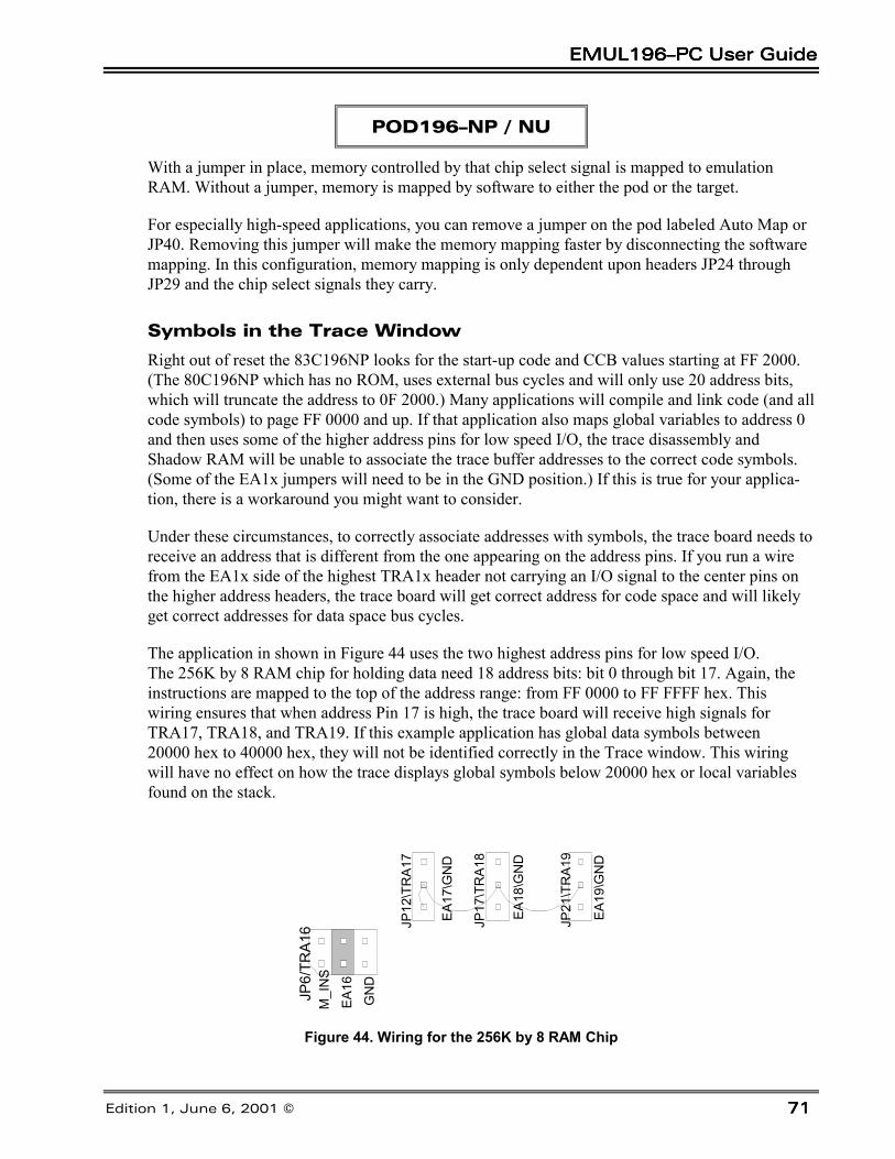
EMUL196–PC User GuideEMUL196–PC User GuideEMUL196–PC User GuideEMUL196–PC User Guide
Edition 1, June 6, 2001 © 717171
POD196–NP / NU
With a jumper in place, memory controlled by that chip select signal is mapped to emulationRAM. Without a jumper, memory is mapped by software to either the pod or the target.
For especially high-speed applications, you can remove a jumper on the pod labeled Auto Map orJP40. Removing this jumper will make the memory mapping faster by disconnecting the softwaremapping. In this configuration, memory mapping is only dependent upon headers JP24 throughJP29 and the chip select signals they carry.
Symbols in the Trace Window
Right out of reset the 83C196NP looks for the start-up code and CCB values starting at FF 2000.(The 80C196NP which has no ROM, uses external bus cycles and will only use 20 address bits,which will truncate the address to 0F 2000.) Many applications will compile and link code (and allcode symbols) to page FF 0000 and up. If that application also maps global variables to address 0and then uses some of the higher address pins for low speed I/O, the trace disassembly andShadow RAM will be unable to associate the trace buffer addresses to the correct code symbols.(Some of the EA1x jumpers will need to be in the GND position.) If this is true for your applica-tion, there is a workaround you might want to consider.
Under these circumstances, to correctly associate addresses with symbols, the trace board needs toreceive an address that is different from the one appearing on the address pins. If you run a wirefrom the EA1x side of the highest TRA1x header not carrying an I/O signal to the center pins onthe higher address headers, the trace board will get correct address for code space and will likelyget correct addresses for data space bus cycles.
The application in shown in Figure 44 uses the two highest address pins for low speed I/O.The 256K by 8 RAM chip for holding data need 18 address bits: bit 0 through bit 17. Again, theinstructions are mapped to the top of the address range: from FF 0000 to FF FFFF hex. Thiswiring ensures that when address Pin 17 is high, the trace board will receive high signals forTRA17, TRA18, and TRA19. If this example application has global data symbols between20000 hex to 40000 hex, they will not be identified correctly in the Trace window. This wiringwill have no effect on how the trace displays global symbols below 20000 hex or local variablesfound on the stack.
M_I
NS
EA17
\GN
D
EA18
\GN
D
EA19
\GN
D
JP12
\TR
A17
JP17
\TR
A18
JP21
\TR
A19
EA16
GN
D
JP6/
TRA1
6
Figure 44. Wiring for the 256K by 8 RAM Chip
Chapter 7. Pod BoardsChapter 7. Pod BoardsChapter 7. Pod BoardsChapter 7. Pod Boards
72727272 EMUL196–PC User Guide
POD196–NP / NU
Mapping Memory Using Chip Selects
While debugging your hardware and software, you typically want to use the RAM on your targetfor data and replace your EPROM with emulation RAM so you can reload and run your applica-tion quickly. Under most circumstances, this can be easily achieved with software memory map-ping. However, on pods with 256K of emulation RAM, address wrapping in the memory mappingscheme can not support all possible target designs.
Essentially, if your design has more than 256K of RAM and ROM combined, you might wantto use the chip select signals instead of software memory mapping to eliminate the addressambiguity.
On pods with 256K of emulation RAM, address bits above bit 17 are ignored. Mapping address10000 hex to the pod also maps 50000 hex, 90000 hex, and D0000 hex to the pod. The chip se-lects, however, do not address wrap. If a chip select signal maps address 10000 hex to the pod,only that address will map to the pod, and not the other addresses.
NotePods sold with 1 MB of emulation RAM have the extra hardware to correctly mapevery address in software. On 1-MB pods, software memory mapping works cor-rectly for all combinations of target RAM and ROM, but can not be fast enough forhigher clock speeds.
To use chip selects to map memory, do the following:
1. Map all addresses to the target.
2. Use a chip select signal (or your target PAL output) to override the software mapping.
3. Remap an address range back to the emulation memory on the pod.
Either this signal can be a chip select signal from the 8xC196NP controller, or it can be the outputfrom some address decoding logic.
WARNING
Mapping all RAM address to a fully functioning target will almost never cause any new problems.However, the emulator cannot function normally when RAM addresses are mapped to nonfunc-tioning RAM.
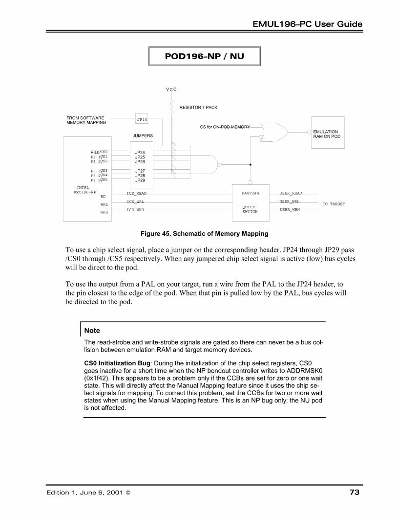
EMUL196–PC User GuideEMUL196–PC User GuideEMUL196–PC User GuideEMUL196–PC User Guide
Edition 1, June 6, 2001 © 737373
POD196–NP / NU
RESISTOR 7 PACK
V C C
FROM SOFTWARE MEMORY MAPPING
JUMPERS
CS for ON-POD MEMORY
EMULATIONRAM ON POD
JP24JP25JP26
JP27
JP29JP28
P3.0/CS0P3.1/CS1P3.2/CS2
P3.3/CS3P3.4/CS4P3.5/CS5
8xC196-NPRD
WRL
WRH
ICE_READ
ICE_WRL
ICE_WRH
USER_READ
USER_WRL
FAST244
QUICKSWITCH USER_WRH
TO TARGET
INTEL
JP40
Figure 45. Schematic of Memory Mapping
To use a chip select signal, place a jumper on the corresponding header. JP24 through JP29 pass/CS0 through /CS5 respectively. When any jumpered chip select signal is active (low) bus cycleswill be direct to the pod.
To use the output from a PAL on your target, run a wire from the PAL to the JP24 header, tothe pin closest to the edge of the pod. When that pin is pulled low by the PAL, bus cycles willbe directed to the pod.
NoteThe read-strobe and write-strobe signals are gated so there can never be a bus col-lision between emulation RAM and target memory devices.
CS0 Initialization Bug: During the initialization of the chip select registers, CS0goes inactive for a short time when the NP bondout controller writes to ADDRMSK0(0x1f42). This appears to be a problem only if the CCBs are set for zero or one waitstate. This will directly affect the Manual Mapping feature since it uses the chip se-lect signals for mapping. To correct this problem, set the CCBs for two or more waitstates when using the Manual Mapping feature. This is an NP bug only; the NU podis not affected.
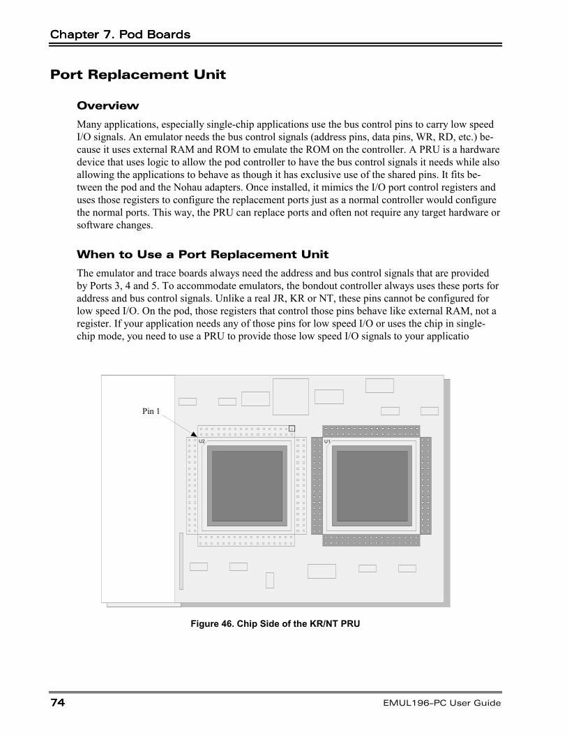
Chapter 7. Pod BoardsChapter 7. Pod BoardsChapter 7. Pod BoardsChapter 7. Pod Boards
74747474 EMUL196–PC User Guide
Port Replacement Unit
Overview
Many applications, especially single-chip applications use the bus control pins to carry low speedI/O signals. An emulator needs the bus control signals (address pins, data pins, WR, RD, etc.) be-cause it uses external RAM and ROM to emulate the ROM on the controller. A PRU is a hardwaredevice that uses logic to allow the pod controller to have the bus control signals it needs while alsoallowing the applications to behave as though it has exclusive use of the shared pins. It fits be-tween the pod and the Nohau adapters. Once installed, it mimics the I/O port control registers anduses those registers to configure the replacement ports just as a normal controller would configurethe normal ports. This way, the PRU can replace ports and often not require any target hardware orsoftware changes.
When to Use a Port Replacement Unit
The emulator and trace boards always need the address and bus control signals that are providedby Ports 3, 4 and 5. To accommodate emulators, the bondout controller always uses these ports foraddress and bus control signals. Unlike a real JR, KR or NT, these pins cannot be configured forlow speed I/O. On the pod, those registers that control those pins behave like external RAM, not aregister. If your application needs any of those pins for low speed I/O or uses the chip in single-chip mode, you need to use a PRU to provide those low speed I/O signals to your applicatio
U2 U1
Pin 1
Figure 46. Chip Side of the KR/NT PRU
EMUL196–PC User GuideEMUL196–PC User GuideEMUL196–PC User GuideEMUL196–PC User Guide
Edition 1, June 6, 2001 © 757575
This one PRU is designed to support all the following processors:
• 8xC196JR, 8xC196KR, 8xC196KS,
• 8xC196JQ, 8xC196KQ, 8xC196NQ,
• 8xC196JT, 8xC196KT, 8xC196NT
• 8xC196CA, 8xC196CB
NoteThe EMUL196-PC PRU/KR/NT Rev. A and Rev. B do not support the 8xC196CAor 8xC196CB
Installing the PRU
To install the PRU, plug the socket on the chip-side of the PRU into the pins on the under side(without the silk screen writing) of the pod board. Ensure that the edges of the PRU line up withthe edges of the pod. Plug the pins all the way into the socket. This might require slightly bendingthe black plastic cover on the pod.
For simplicity, the following paragraphs describing the PRU will only mention the 8xC196KR, butthat text applies equally to targets using other supported controllers. At the end of the PRU sec-tion, there is a paragraph describing 20 bit addressing, not found on the KR part.
PRU Headers and Jumpers
There are six headers with jumpers on this PRU, JP1 through JP6. Five of them are simple to de-scribe and use. The sixth (JP2) is explained in detail in the “PRU Header JP2 – Accessing P3, P4and P5” section later in this chapter. See the following note:
NoteJP2 (intended for Nohau use only) is not installed on the PRU to prevent accidentaluse.
WARNING
Passing through JP1 is the /HLDA signal from Port 2.6. Do not install a jumper on this headerunless instructed to by Nohau Technical Support!
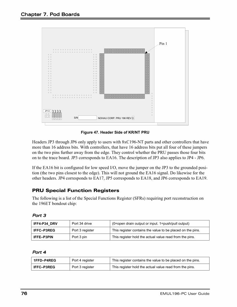
Chapter 7. Pod BoardsChapter 7. Pod BoardsChapter 7. Pod BoardsChapter 7. Pod Boards
76767676 EMUL196–PC User Guide
JP6JP5
JP3JP4
S/N NOHAU CORP. PRU 196 REV D
Pin 1
JP1/2
Figure 47. Header Side of KR/NT PRU
Headers JP3 through JP6 only apply to users with 8xC196-NT parts and other controllers that havemore than 16 address bits. With controllers, that have 16 address bits put all four of these jumperson the two pins further away from the edge. They control whether the PRU passes those four bitson to the trace board. JP3 corresponds to EA16. The description of JP3 also applies to JP4 - JP6.
If the EA16 bit is configured for low speed I/O, move the jumper on the JP3 to the grounded posi-tion (the two pins closest to the edge). This will not ground the EA16 signal. Do likewise for theother headers. JP4 corresponds to EA17, JP5 corresponds to EA18, and JP6 corresponds to EA19.
PRU Special Function Registers
The following is a list of the Special Functions Register (SFRs) requiring port reconstruction onthe 196ET bondout chip:
Port 3Port 3Port 3Port 3
IFF4-P34_DRV Port 34 drive (0=open drain output or input. 1=push/pull output)
IFFC–P3REG Port 3 register This register contains the value to be placed on the pins.
IFFE–P3PIN Port 3 pin This register hold the actual value read from the pins.
Port 4Port 4Port 4Port 4
1FFD–P4REG Port 4 register This register contains the value to be placed on the pins.
IFFC–P3REG Port 3 register This register hold the actual value read from the pins.
EMUL196–PC User GuideEMUL196–PC User GuideEMUL196–PC User GuideEMUL196–PC User Guide
Edition 1, June 6, 2001 © 777777
Port 5Port 5Port 5Port 5
1FF1–P5MODE Port 5 mode register (0=I/O, 1=system function)
1FF3–P5DIR Port 5 I/O register (0=push/pull, 1= input or open drain output)
1FF5–P5REG Port 5 register This register contains the value to be placed on the pins.
IFF7–P5PIN Port 5 pin This register hold the actual value read from the pins.
PRU Reset ValuesPRU Reset ValuesPRU Reset ValuesPRU Reset Values
EA# Pin High EA# Pin Low1FF1=D0H D9H
1FF3=FFH FFH
1FF4=00H 00H
1FF5=FFH FFH
1FFC=FFH FFH
1FFD=FFH FFH
Port 3 and 4 ReconstructionPort 3 and 4 ReconstructionPort 3 and 4 ReconstructionPort 3 and 4 Reconstruction
The 196ET bondout requires the PRU when using any pin of Port 3, 4 or 5 as low speed I/O. ThePOD196–256–KR/NT with the 196ET bondout chip always puts out AD0-AD7 on Port 3 andAD8-AD15 on Port 4. The PRU reconstructs Ports 3 and 4 to mimic the real chip. If externalaccess is made, then the address/data bus is driven on Ports 3 and 4. The following is a list ofdesign details for Port 3 and 4 reconstruction:
• Port 3 and 4 will pass address/data to the target whenever external access is made. The196ET, determines this by the EA# signal address range. When the user ties the EA# pin highand code makes internal access only, then the Port 3 and 4 pins become low speed I/O wherethe values are determined by the values in the Port 3 and 4 SFRs.
• Whenever the user makes external access outside the internal memory range of the chip(determined by the CPU), the PRU will pass the address/data bus to the user on Port 3 and 4instead. As soon as the CPU resumes internal operation, the initial values on the Port 3 and 4pins will be reinserted.
• P3REG and P4REG contain the values to be written to the port pins. P3PIN and P4PIN con-tain the actual value read on the pin itself.
• P34_DRV indicates whether Port 3 or 4 is to be push/pull on an open drain/input.
NoteThe P34_DRV register contains only two important bits:Bit 6 controls whether the entire Port 4 is to be push/pull or an open drain/input.Bit 7 controls whether the entire Port 3 is to be push/pull or an open drain/input.

Chapter 7. Pod BoardsChapter 7. Pod BoardsChapter 7. Pod BoardsChapter 7. Pod Boards
78787878 EMUL196–PC User Guide
Port 5 ReconstructionPort 5 ReconstructionPort 5 ReconstructionPort 5 Reconstruction
The 196ET bondout requires the PRU when you plan to use any pin of Port 5 as low speed I/O.The POD196–KR/NT with the 196ET bondout chip always puts system function signals out onthese pin locations. Therefore, Port 5 reconstruction requires that these same system signals can bepassed to the users target with a maximum 1ns delay (i.e. ALE, RD or WR are critical timing sig-nals). The following is a list of design details for Port 5 reconstruction:
• Port 5 is more complicated to reconstruct than Port 3 and 4 because each pin of Port 5 can beeither a system function or an I/O pin. In addition, each pin has an associated bit that deter-mines if it should be push/pull or open drain/input.
• The PRU does not have access to the CCB bits fetched upon power-up. These bits force acertain mode of operation, therefore a few Port 5 pins are used as a system function upon resetuntil a write is made to the P5MODE register. P5.6 (Ready), P5.7 (BW) and P5.4 (SLPINT)are always a system function upon reset. P5.0 (ALE) and P5.3 (RD#) depend on the EA# pin;these pins are system function only when the EA# pin is low upon reset; otherwise when theEA# pin is high, they are tri-state. All other Port 5 pins are weakly pulled high until a write tothe 5MODE register is made.
• P5REG contains the value to be forced to the pins. P5PIN contains the actual value seen onthe pins. P5DIR contains the direction of each pin (input or output). P5MODE contains themode for each pin (system function or I/O).
Design Limitations and Silicon Bugs—PRU
The bondout chip on the 196ET has a known bug, which affects the performance of the PRU onlywhen you set the CCBs on the chip to 8-bit only mode. In brief, when the 196ET is in 8-bit onlymode and performs writes to odd addresses (using ST or STB instruction), the WRITE HIGH pindoes not work. The only way to get around this is to enter Dynamic buswidth mode by the CCBsand ground the buswidth pin which will automatically place the 196ET into 8-bit mode. A jumperfield (JP5) on the pod will take care of this.
PRU Header JP2—Accessing P3, P4 and P5
NoteIf your application has a 16-bit data bus or if it uses the BW pin to control dynamicbuswidth, you can ignore this section.
This section applies to users of applications were the buswidth bits in the CCBs force an 8-bitwide bus. These users need to read the next few paragraphs to determine if the JP2 header shouldbe shorted or not.
EMUL196–PC User GuideEMUL196–PC User GuideEMUL196–PC User GuideEMUL196–PC User Guide
Edition 1, June 6, 2001 © 797979
The ST instruction stores 16 bits of register data into a 16-bit operator (memory location). TheSTB instruction is similar, but only stores 8 bits at a time. These two instructions interact withthe buswidth and address to create a complicated set of permutations between the instruction used,the buswidth, and whether the data is word aligned or not. Unfortunately, some of these permuta-tions operate differently in the bondout controller than in real KR, JR or NT controllers whenwriting to the PRU.
The PRU can correct these flaws, but only one at a time. If your program sets the buswidth to 8bits by setting the CCB registers, and your program uses both the ST and the STB instruction, oneof those two instructions will operate incorrectly, no matter how you set the jumper on JP2.
As an illustration of what can go wrong, the following table shows the conditions you might en-counter and the jumper settings appropriate to each.
Enter #1234 into a register by executing LD 1C, #1234
Assume that addresses 1FFC and 1FFD contain FF.
8-Bit Store Instructions 16-Bit Store Instructions
CCB Settings of 8xC196 STB 1C, 1FFC STB 1C, 1FFD ST 1C, 1FFC ST 1C, 1FFD
Expected Result(All Modes) FF34 34FF 1234 12FF
JP2 is OUT and:(16-bit only or Dynamic BW or8/16-bit with SRH or BHE Mode) FF34 34FF 1234 12FF
JP2 is OUT and:(8-bit only or BHE Mode) FF34 34FF FF34 * 12FF
JP2 is IN and:(8-bit only or BHE Mode) 3434 * 34FF 1234 12FF
JP2 is OUT and:(8-bit only or WRH Mode) FF34 FFFF * FF34 * FFFF *JP2 is IN and:(8-bit only or WRH Mode) 3434 * FFFF * 1234 FFFF *
* The instructions to these addresses result in errors.
As mentioned previously, most of the time, for most of the permutations, the jumper can be left offand every bus cycle will execute exactly as it does on the real controller. However, if the CCBregisters set the buswidth to 8 bits and your compiler generates ST (16-bit wide store) instructionsto set the Port 3, Port 4 or Port 5 registers, the pod and PRU need header JP2 shorted.
8xC196 vs. POD196 with a PRU8xC196 vs. POD196 with a PRU8xC196 vs. POD196 with a PRU8xC196 vs. POD196 with a PRU
Without a PRU, the SFRs that support low speed I/O on all three ports behave like external RAM,instead of behaving exactly like the same registers in a real KR controller.
This PRU uses two Intel FLEXlogic 780 chips and special features found on the bondout control-ler which, together, do a good job of mimicking Ports 3, 4 and 5. The imitation is close to perfect.Functionally, Port 4 in the PRU and on a real 8xC196KR work identically. Electrically, there are
Chapter 7. Pod BoardsChapter 7. Pod BoardsChapter 7. Pod BoardsChapter 7. Pod Boards
80808080 EMUL196–PC User Guide
some differences that will be described below. Ports 3 and 5 are different in small electrical andfunctional ways. If you are using a PRU, read this section thoroughly, and make some notes inyour 8xC196 manual. Doing so might save you a great deal of time.
Port 3Port 3Port 3Port 3Port 3 is functionally identical to Port 3 on the controller.
Electrically, there are two small differences between the controller Port 3 and the PRU Port 3.Every pin on KR Port 3 is specified to sink at least 3 mA at 0.45V and source at least –3 mA atVcc-0.7V. Instead, the PRU Port 3 pins can sink 12 mA and source –4 mA.
Port 4Port 4Port 4Port 4Port 4 is functionally identical on the controller and on the PRU.
Like Port 3, electrically, there are two small differences between the controller Port 4 and the PRUPort 4. Every pin on a KR Port 4 is specified to sink at least 3 mA at 0.45V and source at least –3mA at Vcc-0.7V. Instead, the PRU Port 4 can sink 12 mA and source –4 mA.
Port 5Port 5Port 5Port 5The design of Port 5 is different than Ports 3 and 4. In the Intel User’s Manual, Figure 10.3 showsthe circuit schematic for Port 5. Compare Figure 49 with Figure 48 for changes to the port circuit.QW has been replaced by a 100K Ohm pull-up resistor which approximately matches the weakpull-up current provided by QW during /RESET.
In the PRU, the transistors driving the Port 5 pins are slightly different. In the 8xC196KR, transis-tor QL can sink at least 3 mA at 0.45V. In the PRU, that transistor can sink 12 mA. Likewise, QUcan source at least –3 mA at Vcc-0.7V. In the PRU, that transistor can source –4 mA.
If you compare Figure 48 to Figure 49, you will notice two major differences. /WKPU in the con-troller has been replaced by a normal pull-up resistor and a 100K Ohm resistor, and the –300 nsdelay in the RESET portion of the circuit is not present in the PRU. Functionally, the differencesbetween the port and the PRU are in the registers.
Vcc
Vcc
QL
I/O PIN
P5_PIN
RESET
QU
Vcc
-300nS DELAY
WKPU
PPU
S
RQ
RESET
ANY WRITE TO PxMODE
Figure 48. 8xC196 Port 5 Circuit
EMUL196–PC User GuideEMUL196–PC User GuideEMUL196–PC User GuideEMUL196–PC User Guide
Edition 1, June 6, 2001 © 818181
Vcc
QL
I/O PIN
P5_PIN
QU
Vcc
S
RQ
RESET
ANY WRITE TO PxMODE
100K Ohm
QPU
Figure 49. PRU Port 5 Circuit

Chapter 7. Pod BoardsChapter 7. Pod BoardsChapter 7. Pod BoardsChapter 7. Pod Boards
82828282 EMUL196–PC User Guide
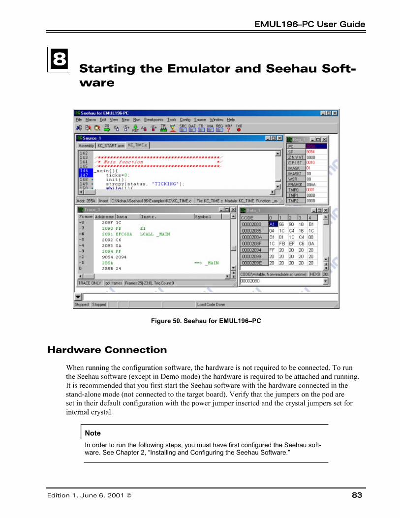
EMUL196–PC User GuideEMUL196–PC User GuideEMUL196–PC User GuideEMUL196–PC User Guide
Edition 1, June 6, 2001 © 838383
Starting the Emulator and Seehau Soft-ware
Figure 50. Seehau for EMUL196–PC
Hardware Connection
When running the configuration software, the hardware is not required to be connected. To runthe Seehau software (except in Demo mode) the hardware is required to be attached and running.It is recommended that you first start the Seehau software with the hardware connected in thestand-alone mode (not connected to the target board). Verify that the jumpers on the pod areset in their default configuration with the power jumper inserted and the crystal jumpers set forinternal crystal.
NoteIn order to run the following steps, you must have first configured the Seehau soft-ware. See Chapter 2, “Installing and Configuring the Seehau Software.”
Chapter 8. Starting the Emulator and Seehau SoftwareChapter 8. Starting the Emulator and Seehau SoftwareChapter 8. Starting the Emulator and Seehau SoftwareChapter 8. Starting the Emulator and Seehau Software
84848484 EMUL196–PC User Guide
Starting Seehau
To start the Seehau software, do the following:
1. Double-click the Seehau 196 icon. The Seehau main window opens (Figure 50). Seehau willload its configuration from the Startup.bas file. The macro is displayed in red at the bottom ofthe main window while Startup.bas is running.
2. While the software is starting, the reset light goes on and off, resetting the pod. Whenthe software has completed its startup, you can position and resize the main window toyour preference.
3. To open new windows, click the New menu, and then select the type of window you want fromthe list.
NoteIf you are using an HSP or USB box, make sure that you have the box powered onprior to starting the software. If the box is not powered on you will receive an errormessage when the software tries to initialize the hardware. In order to clear theerror, you may have to quit the software and restart it.
4. If you receive a fatal error when starting the Seehau software, see Appendix A, “Trouble-shooting”, or contact Nohau Technical Support at [email protected].
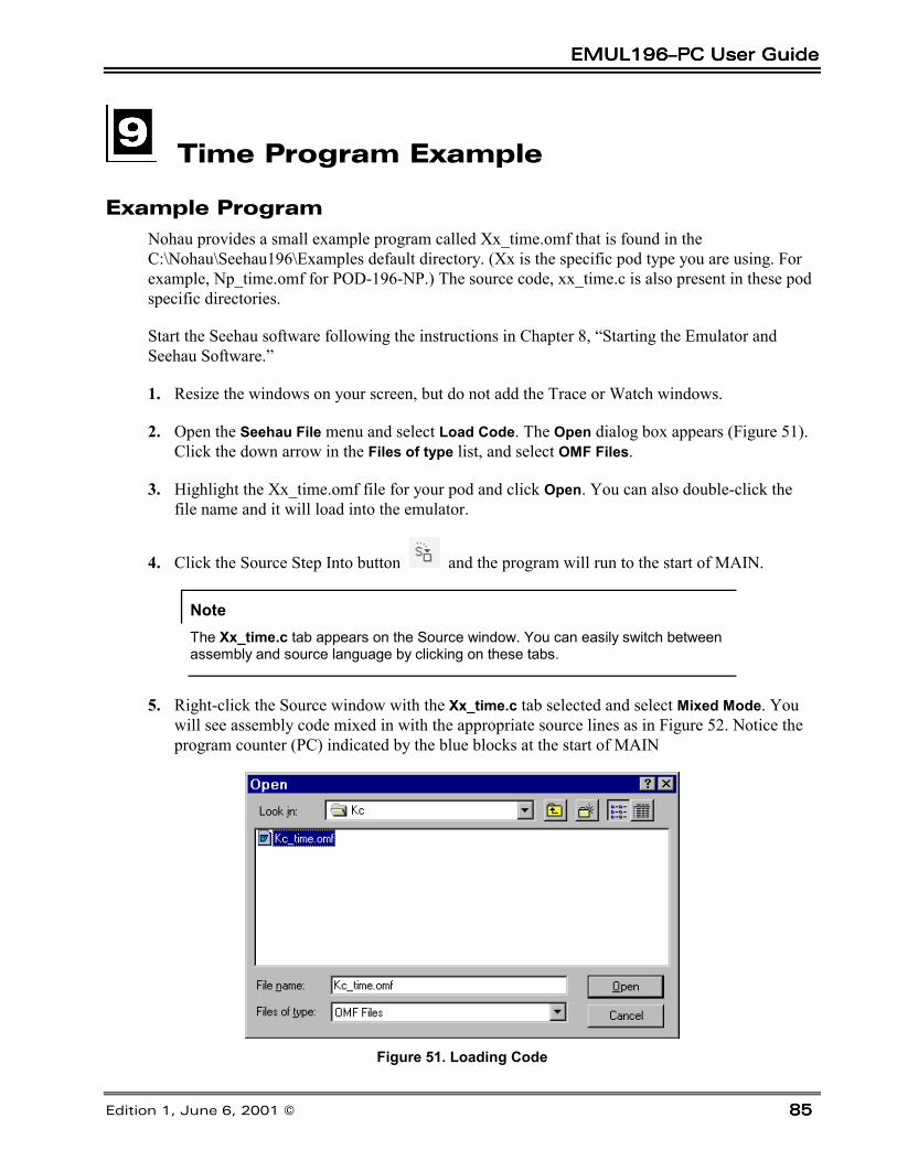
EMUL196–PC User GuideEMUL196–PC User GuideEMUL196–PC User GuideEMUL196–PC User Guide
Edition 1, June 6, 2001 © 858585
Time Program Example
Example ProgramNohau provides a small example program called Xx_time.omf that is found in theC:\Nohau\Seehau196\Examples default directory. (Xx is the specific pod type you are using. Forexample, Np_time.omf for POD-196-NP.) The source code, xx_time.c is also present in these podspecific directories.
Start the Seehau software following the instructions in Chapter 8, “Starting the Emulator andSeehau Software.”
1. Resize the windows on your screen, but do not add the Trace or Watch windows.
2. Open the Seehau File menu and select Load Code. The Open dialog box appears (Figure 51).Click the down arrow in the Files of type list, and select OMF Files.
3. Highlight the Xx_time.omf file for your pod and click Open. You can also double-click thefile name and it will load into the emulator.
4. Click the Source Step Into button and the program will run to the start of MAIN.
NoteThe Xx_time.c tab appears on the Source window. You can easily switch betweenassembly and source language by clicking on these tabs.
5. Right-click the Source window with the Xx_time.c tab selected and select Mixed Mode. Youwill see assembly code mixed in with the appropriate source lines as in Figure 52. Notice theprogram counter (PC) indicated by the blue blocks at the start of MAIN
Figure 51. Loading Code
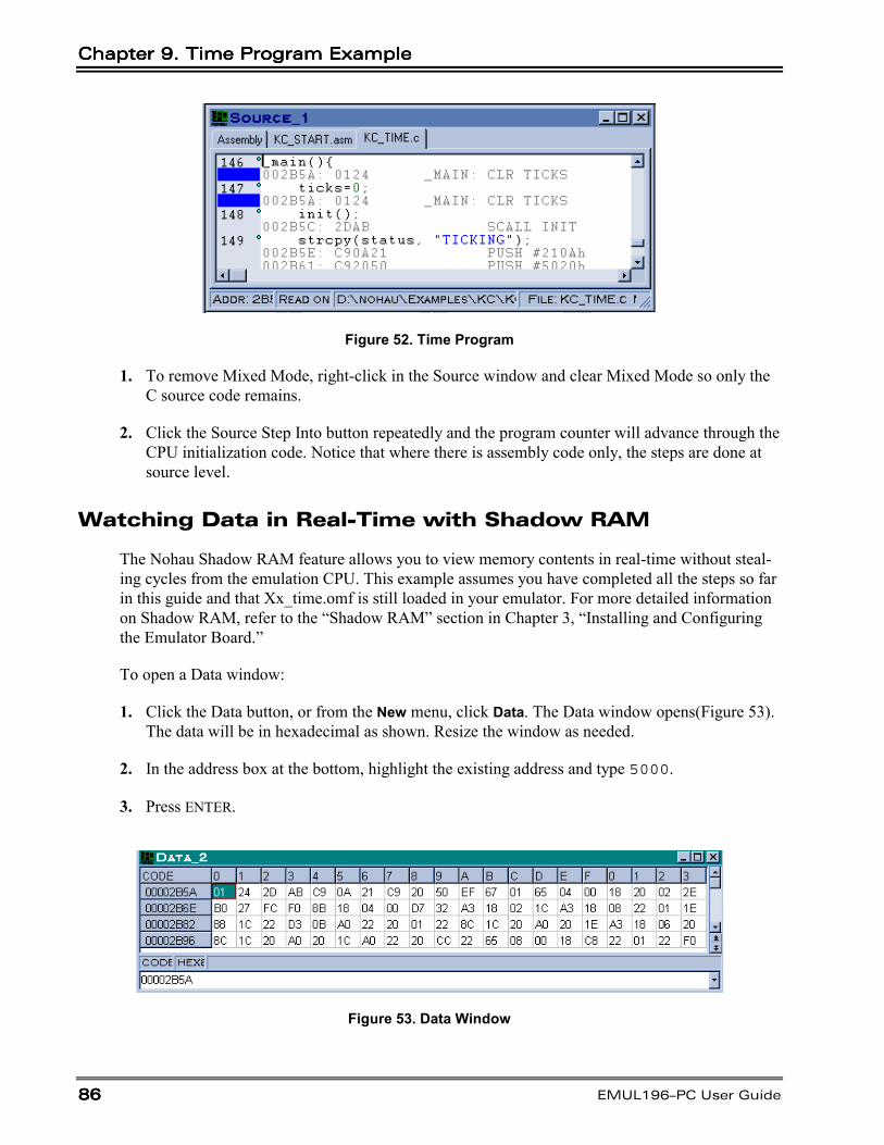
Chapter 9. Time Program ExampleChapter 9. Time Program ExampleChapter 9. Time Program ExampleChapter 9. Time Program Example
86868686 EMUL196–PC User Guide
Figure 52. Time Program
1. To remove Mixed Mode, right-click in the Source window and clear Mixed Mode so only theC source code remains.
2. Click the Source Step Into button repeatedly and the program counter will advance through theCPU initialization code. Notice that where there is assembly code only, the steps are done atsource level.
Watching Data in Real-Time with Shadow RAM
The Nohau Shadow RAM feature allows you to view memory contents in real-time without steal-ing cycles from the emulation CPU. This example assumes you have completed all the steps so farin this guide and that Xx_time.omf is still loaded in your emulator. For more detailed informationon Shadow RAM, refer to the “Shadow RAM” section in Chapter 3, “Installing and Configuringthe Emulator Board.”
To open a Data window:
1. Click the Data button, or from the New menu, click Data. The Data window opens(Figure 53).The data will be in hexadecimal as shown. Resize the window as needed.
2. In the address box at the bottom, highlight the existing address and type 5000.
3. Press ENTER.
Figure 53. Data Window
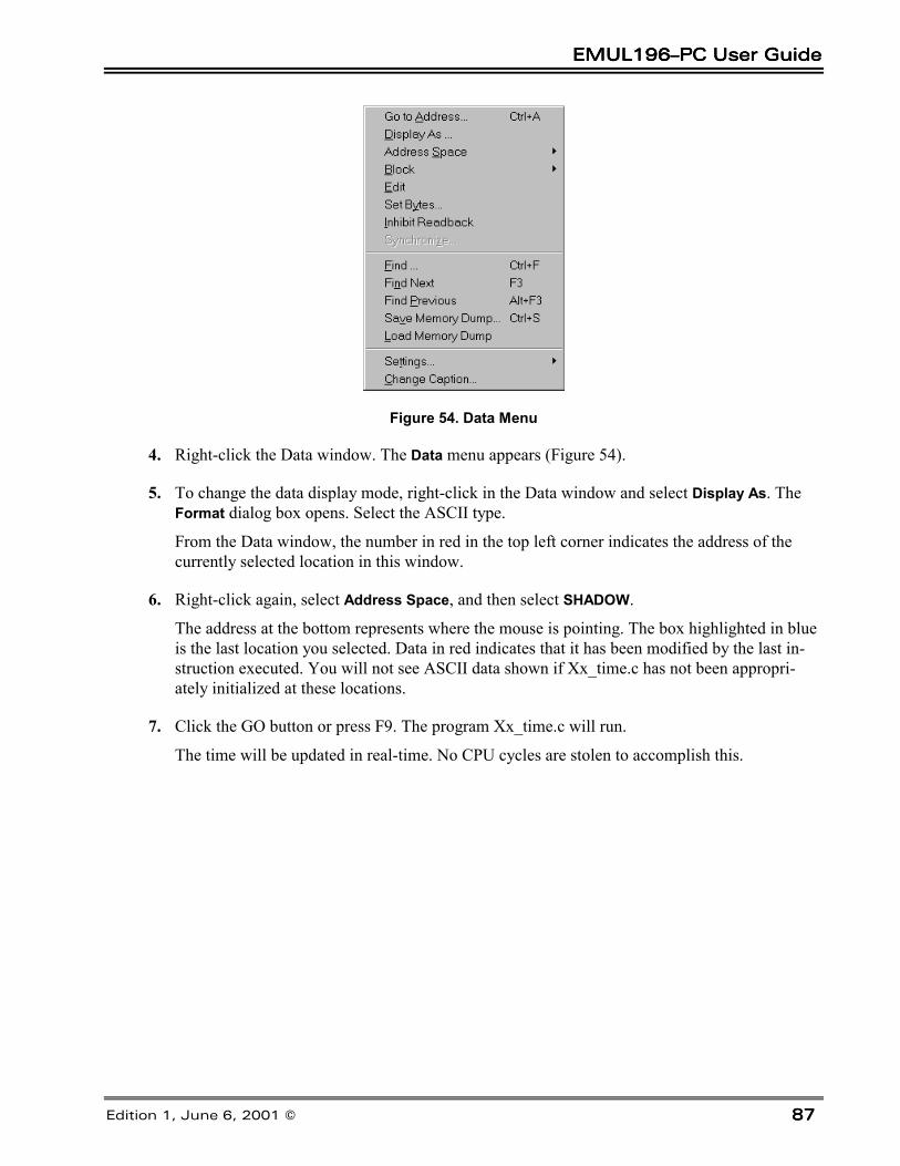
EMUL196–PC User GuideEMUL196–PC User GuideEMUL196–PC User GuideEMUL196–PC User Guide
Edition 1, June 6, 2001 © 878787
Figure 54. Data Menu
4. Right-click the Data window. The Data menu appears (Figure 54).
5. To change the data display mode, right-click in the Data window and select Display As. TheFormat dialog box opens. Select the ASCII type.
From the Data window, the number in red in the top left corner indicates the address of thecurrently selected location in this window.
6. Right-click again, select Address Space, and then select SHADOW.
The address at the bottom represents where the mouse is pointing. The box highlighted in blueis the last location you selected. Data in red indicates that it has been modified by the last in-struction executed. You will not see ASCII data shown if Xx_time.c has not been appropri-ately initialized at these locations.
7. Click the GO button or press F9. The program Xx_time.c will run.
The time will be updated in real-time. No CPU cycles are stolen to accomplish this.

Chapter 9. Time Program ExampleChapter 9. Time Program ExampleChapter 9. Time Program ExampleChapter 9. Time Program Example
88888888 EMUL196–PC User Guide
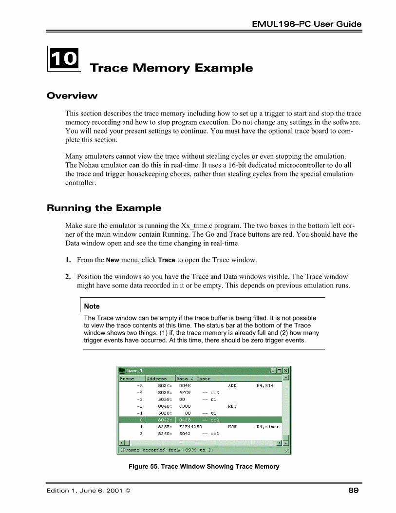
EMUL196–PC User GuideEMUL196–PC User GuideEMUL196–PC User GuideEMUL196–PC User Guide
Edition 1, June 6, 2001 © 898989
Trace Memory Example
Overview
This section describes the trace memory including how to set up a trigger to start and stop the tracememory recording and how to stop program execution. Do not change any settings in the software.You will need your present settings to continue. You must have the optional trace board to com-plete this section.
Many emulators cannot view the trace without stealing cycles or even stopping the emulation.The Nohau emulator can do this in real-time. It uses a 16-bit dedicated microcontroller to do allthe trace and trigger housekeeping chores, rather than stealing cycles from the special emulationcontroller.
Running the Example
Make sure the emulator is running the Xx_time.c program. The two boxes in the bottom left cor-ner of the main window contain Running. The Go and Trace buttons are red. You should have theData window open and see the time changing in real-time.
1. From the New menu, click Trace to open the Trace window.
2. Position the windows so you have the Trace and Data windows visible. The Trace windowmight have some data recorded in it or be empty. This depends on previous emulation runs.
NoteThe Trace window can be empty if the trace buffer is being filled. It is not possibleto view the trace contents at this time. The status bar at the bottom of the Tracewindow shows two things: (1) if, the trace memory is already full and (2) how manytrigger events have occurred. At this time, there should be zero trigger events.
Figure 55. Trace Window Showing Trace Memory
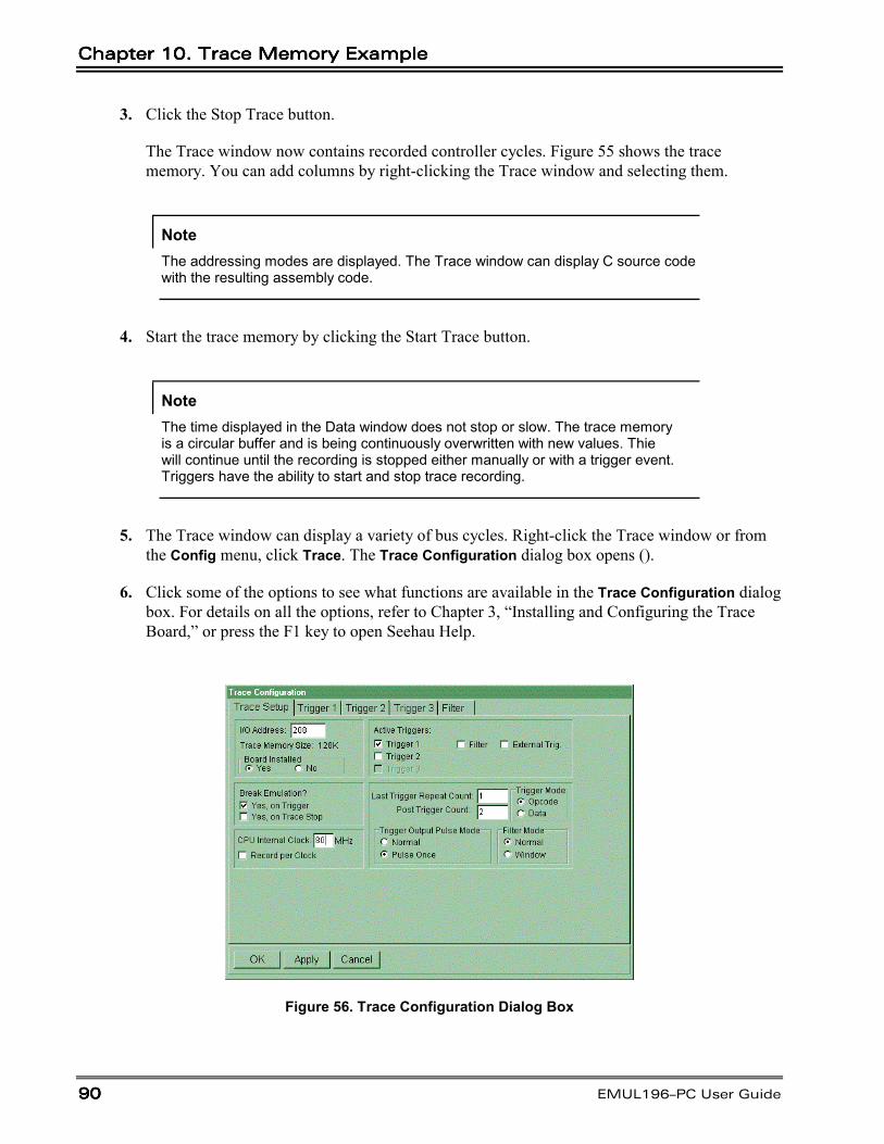
Chapter 10. Trace Memory ExampleChapter 10. Trace Memory ExampleChapter 10. Trace Memory ExampleChapter 10. Trace Memory Example
90909090 EMUL196–PC User Guide
3. Click the Stop Trace button.
The Trace window now contains recorded controller cycles. Figure 55 shows the tracememory. You can add columns by right-clicking the Trace window and selecting them.
NoteThe addressing modes are displayed. The Trace window can display C source codewith the resulting assembly code.
4. Start the trace memory by clicking the Start Trace button.
NoteThe time displayed in the Data window does not stop or slow. The trace memoryis a circular buffer and is being continuously overwritten with new values. Thiewill continue until the recording is stopped either manually or with a trigger event.Triggers have the ability to start and stop trace recording.
5. The Trace window can display a variety of bus cycles. Right-click the Trace window or fromthe Config menu, click Trace. The Trace Configuration dialog box opens ().
6. Click some of the options to see what functions are available in the Trace Configuration dialogbox. For details on all the options, refer to Chapter 3, “Installing and Configuring the TraceBoard,” or press the F1 key to open Seehau Help.
Figure 56. Trace Configuration Dialog Box
EMUL196–PC User GuideEMUL196–PC User GuideEMUL196–PC User GuideEMUL196–PC User Guide
Edition 1, June 6, 2001 © 919191
Saving the Configuration
1. To save the Emulator configuration, click the Config menu and select Save Emul Cfg.
2. To save the Trace configuration, click the Config menu and select Save Trace Cfg.
3. The Save Settings dialog box opens where you can choose the filename for the newly createdmacro. Enter a filename of your choosing and click Save.
The macro is ready to use and will be accurately recreate your emulator configuration settings.Configuration settings are also saved when general Seehau settings are saved.
Chapter 10. Trace Memory ExampleChapter 10. Trace Memory ExampleChapter 10. Trace Memory ExampleChapter 10. Trace Memory Example
92929292 EMUL196–PC User Guide
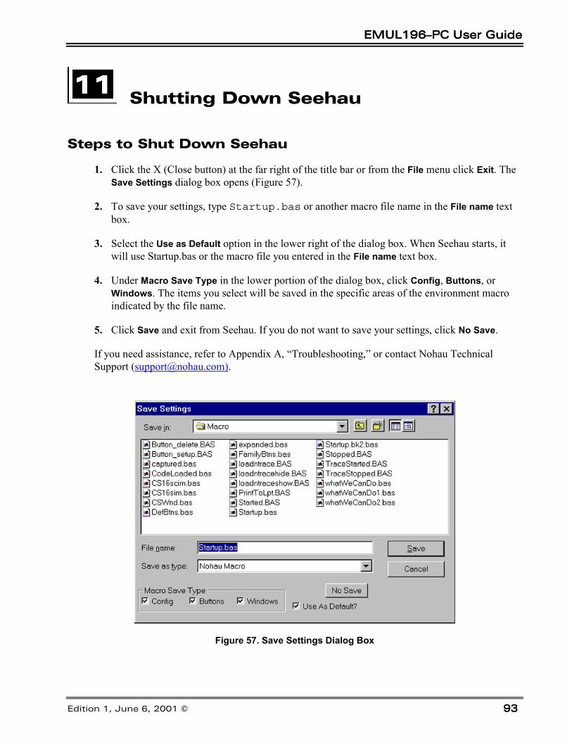
EMUL196–PC User GuideEMUL196–PC User GuideEMUL196–PC User GuideEMUL196–PC User Guide
Edition 1, June 6, 2001 © 939393
Shutting Down Seehau
Steps to Shut Down Seehau
1. Click the X (Close button) at the far right of the title bar or from the File menu click Exit. TheSave Settings dialog box opens (Figure 57).
2. To save your settings, type Startup.bas or another macro file name in the File name textbox.
3. Select the Use as Default option in the lower right of the dialog box. When Seehau starts, itwill use Startup.bas or the macro file you entered in the File name text box.
4. Under Macro Save Type in the lower portion of the dialog box, click Config, Buttons, orWindows. The items you select will be saved in the specific areas of the environment macroindicated by the file name.
5. Click Save and exit from Seehau. If you do not want to save your settings, click No Save.
If you need assistance, refer to Appendix A, “Troubleshooting,” or contact Nohau TechnicalSupport ([email protected]).
Figure 57. Save Settings Dialog Box
Chapter 11. Shutting Down SeehauChapter 11. Shutting Down SeehauChapter 11. Shutting Down SeehauChapter 11. Shutting Down Seehau
94949494 EMUL196–PC User Guide
Important Software and Hardware Notes
Always use Uninstall to unload any existing version of Seehau from your computer before loadinganother copy. Do not simply delete the Seehau files or folders. Do not install Seehau on top of anexisting copy.
To use Uninstall, do the following:
1. In My Computer, double-click Control Panel.
2. Double-click Add/Remove Programs.
3. A list of installed programs is shown.
4. Select (highlight) the Seehau 196 and click Add/Remove. (In this case it will remove theselected program.)
5. Backup your personal macros and source files into another directory before uninstalling theSeehau software. (The Macro subdirectory is not usually deleted on the uninstall, but as a pre-caution you should always backup your files before starting this process.)

EMUL196–PC User GuideEMUL196–PC User GuideEMUL196–PC User GuideEMUL196–PC User Guide
Edition 1, June 6, 2001 © 959595
Appendix A. Troubleshooting
Overview
In many cases, if you are having trouble with the Seehau software and need help one of the fastestand easiest ways to get an answer is to select Seehau Help. While this might not answer all ques-tions it is a valuable resource and should be used before calling technical support.
If you have trouble with your emulator, you can contact Nohau Technical Support at 1-888-886-6428 or email us at [email protected]. If you contact us, the engineer will likely lead youthrough the following steps to test for the most common problems. To save time, you can also testfor the problems by looking over this section to determine if your problem is describe here.
The items to check for are in order following this section. Start at the first item and continueuntil the emulator works or you have reached the end of the list. Each item is a short version ofa description from earlier in this guide. Most items have at least one chapter number where moredetails can be found.
If you encounter a problem when starting or running the emulator and/or Seehau, try the followingtroubleshooting tips. For detailed troubleshooting instructions, contact Nohau Technical Support [email protected].
WARNING
Always turn the power off before you plug in or unplug boards, ribbon cables, or the pod board toavoid hardware damage.
Before you start troubleshooting, first check the following items:
• Are the cables connected properly?
• If you are using an HSP or USB box, is the power turned on?
• Did you remove any foam that might be present on the bottom pins of the pod?
• If the pod is not connected to your target, are the power and crystal jumpers/switches in thePOD position?
• If the pod is connected to your target, is the target power turned on?
• Is the pod connected to the emulator board?
Appendix A. TroubleshootingAppendix A. TroubleshootingAppendix A. TroubleshootingAppendix A. Troubleshooting
96969696 EMUL196–PC User Guide
• Verify the proper pod type is selected, and jumper configurations match the default configu-ration. (Refer to Chapter 6, “Installing and Configuring the Pod Boards,” and Chapter 7, “PodBoards” for your specific pod type.)
• Determine if the emulator and pod operate together when not connected to the target system.Remove the pod from the target and attempt to start the system in stand-alone mode. Theemulator does not require a target. To troubleshoot in stand-alone mode, make sure the powerjumper is selected for internal power and the crystal (clock) jumpers are in the pod position.(Refer to Chapter 7, “Pod Boards.”)
• Did you configure Seehau correctly for your MCU and pod?
• Open the Task Manager and check that ncore is no longer running after an access violation.
• Verify there is no address conflict with the PC. If you are using the default emulator board ad-dress (200), make sure that there is no other device using 200 – 208 in your PC. For example,a game port is usually located at address 201. If there is a conflict, refer to Chapter 3,“Installing and Configuring the Emulator Board” on how to select another address.
• If you have trouble printing while the printer is connected to the HSP, be aware that the HSPmust be powered on for the printer to receive printer port signals. (See the “Debugging theParallel Port” section later in this chapter.
• Reload Seehau. To reload, use the Windows Add/Remove Programs option. This ensures allfiles and registry entries are properly deleted. To access the Add/Remove Programs Proper-ties dialog box, go to the Start menu and point to Settings. Click Control Panel. Double-clickAdd/Remove Programs.
• Try another PC.
Stack Pointer
Because the emulator pushes the return address on the stack, the Stack Pointer must point to validmemory. There must be room on the stack for two bytes (or four bytes for users of chips withlarger addressable ranges) to hold the address.
CAUTION
In addition, there is a lower limit to the stack pointer. The stack pointer must have a value greaterthan 0x50, or else your register contents cannot be saved correctly.
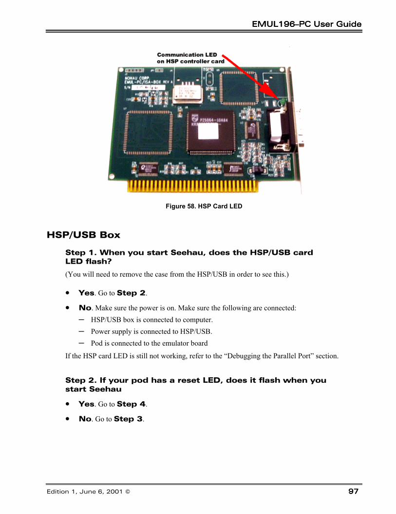
EMUL196–PC User GuideEMUL196–PC User GuideEMUL196–PC User GuideEMUL196–PC User Guide
Edition 1, June 6, 2001 © 979797
Figure 58. HSP Card LED
HSP/USB Box
Step 1. When you start Seehau, does the HSP/USB cardLED flash?
(You will need to remove the case from the HSP/USB in order to see this.)
• Yes. Go to Step 2.
• No. Make sure the power is on. Make sure the following are connected:– HSP/USB box is connected to computer.– Power supply is connected to HSP/USB.– Pod is connected to the emulator board
If the HSP card LED is still not working, refer to the “Debugging the Parallel Port” section.
Step 2. If your pod has a reset LED, does it flash when youstart Seehau
• Yes. Go to Step 4.
• No. Go to Step 3.
Appendix A. TroubleshootingAppendix A. TroubleshootingAppendix A. TroubleshootingAppendix A. Troubleshooting
98989898 EMUL196–PC User Guide
Step 3. Do board I/O addresses match the values in theSeehau configuration?
If your reset LED does not flash or your pod is not equipped with a reset LED, verify that theboard I/O addresses (for emulator and trace boards) match the values in the Seehau Configuration:
• Yes. The I/O addresses match the values:1. From the Start menu, select Programs.
2. Select Seehau196, then click Config. If the board I/O addresses match the values in theSeehau configuration, go to the “Configuring Address Settings with Windows OperatingSystems” section in Chapter 2. Pay specific attention to alternate addressing.
If you still encounter problems, contact Nohau Technical Support.
• No. The I/O addresses do not match the values:1. From the Start menu, select Programs.
2. Select SeehauHC11 and click Reconfig.
3. Enter the appropriate values.
• Yes. The reset LED flashes.
Does Seehau start?
– Yes. Troubleshooting is complete!– No. The reset LED does not flash. Contact Nohau Technical Support.
NoteWe suggest that you remove the pod from the target when you do the followingsteps.
EMUL196–PC User GuideEMUL196–PC User GuideEMUL196–PC User GuideEMUL196–PC User Guide
Edition 1, June 6, 2001 © 999999
Debugging the Parallel Port
Step 1. Disconnect other devices that might be sharing this parallel port (such as printers, zip,or jazz drives, parallel CD ROM drives, or software dongle keys).
Now is it working?
• Yes. You’re done. You might opt to purchase an additional parallel port card.
• No. Do the following:
Windows NT Users
Check the Nohau196 driver status by doing the following:
• To check the status, go to the Start menu. Select Control Panel. Then double-click Devices.
– If the status shows Started, go to Step 2.– If the status shows Stopped, check the ParPort driver for Started status.– If the ParPort driver shows Stopped click Start.
• Now re-check the driver status.– If the driver shows Started, try restarting Seehau.– If the ParPort driver still shows Stopped, go to NT Diagnostics:
1. From the Start menu, select Programs.
2. Then select Administrative Tools, and click Windows NT Diagnostics. The Windows NTDiagnostics window opens.
3. Click the Resources tab.
4. Click I/O Port. Scroll down to address 378 (LPT1) and look for a device at this address.
5. From the Control Panel, double-click Devices. Disable the device located at 378.
6. Attempt to restart Seehau. If this fails, go to Step 2.
Windows 9x Users
Check the parallel port mode. Go to Step 2.
Windows 2000 Users
Verify that the Nohau196 device driver is properly installed. Do the following:
1. From the Start menu, select Programs. Select Accessories, then click System Tools.
2. Double-click System Information. The System Information window opens (Figure 59).
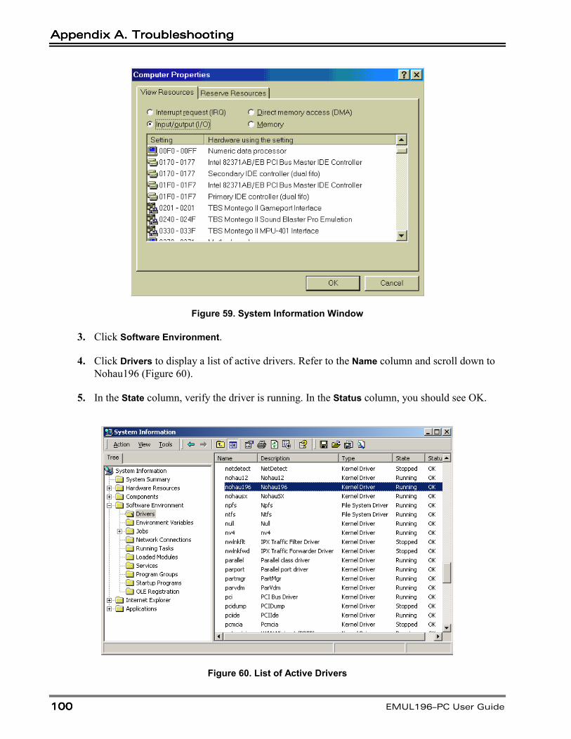
Appendix A. TroubleshootingAppendix A. TroubleshootingAppendix A. TroubleshootingAppendix A. Troubleshooting
100100100100 EMUL196–PC User Guide
Figure 59. System Information Window
3. Click Software Environment.
4. Click Drivers to display a list of active drivers. Refer to the Name column and scroll down toNohau196 (Figure 60).
5. In the State column, verify the driver is running. In the Status column, you should see OK.
Figure 60. List of Active Drivers
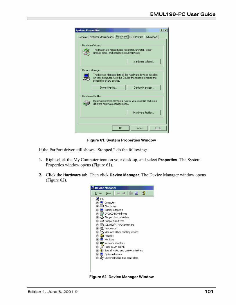
EMUL196–PC User GuideEMUL196–PC User GuideEMUL196–PC User GuideEMUL196–PC User Guide
Edition 1, June 6, 2001 © 101101101
Figure 61. System Properties Window
If the ParPort driver still shows “Stopped,” do the following:
1. Right-click the My Computer icon on your desktop, and select Properties. The SystemProperties window opens (Figure 61).
2. Click the Hardware tab. Then click Device Manager. The Device Manager window opens(Figure 62).
Figure 62. Device Manager Window
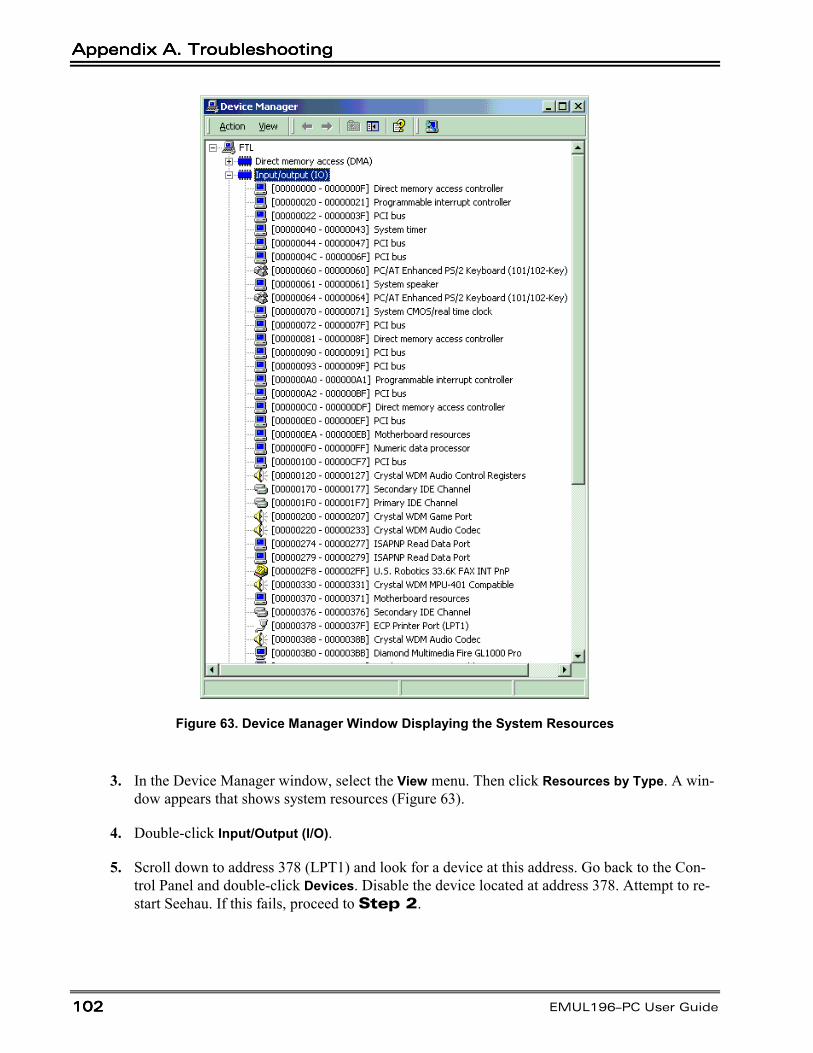
Appendix A. TroubleshootingAppendix A. TroubleshootingAppendix A. TroubleshootingAppendix A. Troubleshooting
102102102102 EMUL196–PC User Guide
Figure 63. Device Manager Window Displaying the System Resources
3. In the Device Manager window, select the View menu. Then click Resources by Type. A win-dow appears that shows system resources (Figure 63).
4. Double-click Input/Output (I/O).
5. Scroll down to address 378 (LPT1) and look for a device at this address. Go back to the Con-trol Panel and double-click Devices. Disable the device located at address 378. Attempt to re-start Seehau. If this fails, proceed to Step 2.
EMUL196–PC User GuideEMUL196–PC User GuideEMUL196–PC User GuideEMUL196–PC User Guide
Edition 1, June 6, 2001 © 103103103
Step 2. Check the parallel port mode.
1. Reboot and enter BIOS setup. From BIOS setup, check for one of the following parallel portmodes:– Normal– Standard– Compatible– Output only– Bi-directional– AT– PS/2
NoteThere might be more or other modes listed in your computer BIOS. You might tryseveral before the correct mode is found. (See the following Note.)
2. Ensure that one of these modes is selected.
3. Then try selecting another mode.
4. Save your settings and reboot.
NoteThe following modes have been known to cause problems: ECP, EPP, or ECP +EPP.
Appendix A. TroubleshootingAppendix A. TroubleshootingAppendix A. TroubleshootingAppendix A. Troubleshooting
104104104104 EMUL196–PC User Guide
ISA
Step 1. Does the pod reset LED flash when you start Seehau?
• Yes. Go to Step 3.
• No. Go to Step 2.
Step 2. Do board I/O addresses match the values in theSeehau configuration?
If your reset LED does not flash, verify that the board I/O addresses (for emulator and traceboards) match the values in the Seehau Configuration:
• Yes. The I/O addresses match the values:
1. From the Start menu, select Programs.
2. Select Seehau196, then click Config. If the board I/O addresses match the values in the Seehauconfiguration, go to the “Configuring Address Settings with Windows Operating Systems” section inChapter 2. Pay specific attention to alternate addressing.
If you still encounter problems, contact Nohau Technical Support.
• No. The I/O addresses do not match the values:
1. From the Start menu, select Programs.
2. Select Seehau196 and click Config.
3. Enter the appropriate values.
Now does the reset LED flash?
• Yes. The reset LED flashes.
Does Seehau start?
– Yes. Troubleshooting is complete!– No. Seehau does not start. Go to Step 3.– No. The reset LED does not flash. Contact Nohau Technical Support.
Step 3. Will Seehau start if you configure for test modeafter reset?
• Yes. Refer to Chapter 6, “Installing and Configuring the Pod Boards,” and Chapter 7,“Pod Boards.”
• No. Refer to Chapter 3, “Installing and Configuring the Emulator Board,” and Chapter 4,“Installing and Configuring the Trace Board.” Review the “Configuring Address SettingsWith Windows Operating Systems” section in Chapter 2.
EMUL196–PC User GuideEMUL196–PC User GuideEMUL196–PC User GuideEMUL196–PC User Guide
Edition 1, June 6, 2001 © 105105105
Is the problem solved?– Yes. Troubleshooting is complete!– No. Contact Nohau Technical Support.
If the Emulator Does Not Start When Connected to theTarget System
• Make sure power is applied to the target system.
• If the target has a watchdog timer, disconnect the watchdog circuitry on your target, or re-move JP14 on the pod. This will disconnect the reset signal going from your target to the resetpin on the controller.
• Try switching the crystal jumpers/switches to the TARGET position.
• Disconnect the target. Make sure you change the crystal and power jumpers/switches to thePOD position. Then try restarting the Seehau software.
• Check the orientation of the target adapter. Confirm that the adapter is inserted properly. Formore information start the “View Adapter” software included on the Nohau software CD.
• Check for grounding problems. The emulator and target should have a solid common ground.Targets that are improperly grounded or designed with a floating ground might experienceimproper operation. A closer examination of control signals might reveal excessive over /undershoot or ground noise.
• If you are able to start the emulator, the problem is with one or more of the following criticaltarget signals:
– address and data bus– clock
Board I/O Addresses
Confirm that the I/O address set in the jumpers on the emulator and trace boards both agree withthe software settings found in their respective configuration dialog boxes.
Appendix A. TroubleshootingAppendix A. TroubleshootingAppendix A. TroubleshootingAppendix A. Troubleshooting
106106106106 EMUL196–PC User Guide
Emulator Configuration Utility Screen
The Seehau software is used for all EMUL196–PC products. The type of target processor in thesoftware configuration must agree with the type of pod you are using. If not, you might see a FatalStartup error message. To ensure that you do not get this error, Nohau includes a utility that youcan run when you first install the emulator, and possibly, again when you run change your podtype. This utility is called Config. (You can also run this utility any time you want to check thevalues in the initialization file.)
To invoke Config:
1. Click on the Start icon in the lower corner of your monitor. A list of options will appear.
2. Move your cursor up until Programs is highlighted. A secondary list of programs and optionswill appear.
3. Move your cursor until you highlight Seehau 196. Another list will appear.
4. Move your cursor over the Config option and click on it. The Emulator Configuration (Com-munications) dialog box opens.
5. Select your method of connection (HSP, ISA, LC-ISA or USB).
6. Click on the picture that represents your equipment.
7. Click Next after each selection. After the last selection on the first dialog box, the Hdw Configdialog box opens.
8. Make the appropriate selection on the options you want.
9. When you are finished selecting your options, select Finish.
You are now ready to run your program with the options you selected and the emulator will start.
You can also start this procedure by clicking on the Seehau196 icon on your desktop and follow-ing the same procedure from the first frame of the Emulator Configuration dialog box. (Thismethod will require you to delete the file Startup.bas first.)
PWR and XTAL Jumpers
If there is a power supply on the target, remove the PWR jumper from the pod. If the crystal oroscillator on the target is running at a different frequency than the one on the pod board, move theXTAL jumpers to the target position.
For more information, see the section in Chapter 7, “Pod Boards” that describes the kind of podyou have.
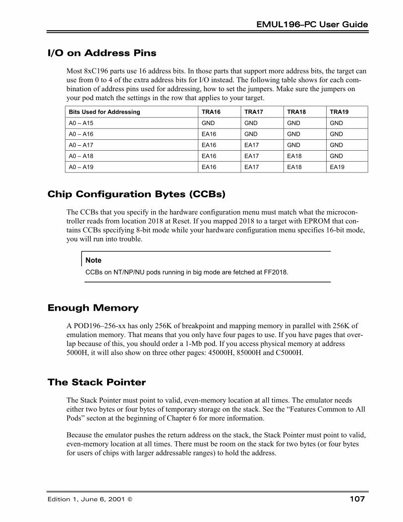
EMUL196–PC User GuideEMUL196–PC User GuideEMUL196–PC User GuideEMUL196–PC User Guide
Edition 1, June 6, 2001 © 107107107
I/O on Address Pins
Most 8xC196 parts use 16 address bits. In those parts that support more address bits, the target canuse from 0 to 4 of the extra address bits for I/O instead. The following table shows for each com-bination of address pins used for addressing, how to set the jumpers. Make sure the jumpers onyour pod match the settings in the row that applies to your target.
Bits Used for Addressing TRA16 TRA17 TRA18 TRA19
A0 – A15 GND GND GND GND
A0 – A16 EA16 GND GND GND
A0 – A17 EA16 EA17 GND GND
A0 – A18 EA16 EA17 EA18 GND
A0 – A19 EA16 EA17 EA18 EA19
Chip Configuration Bytes (CCBs)
The CCBs that you specify in the hardware configuration menu must match what the microcon-troller reads from location 2018 at Reset. If you mapped 2018 to a target with EPROM that con-tains CCBs specifying 8-bit mode while your hardware configuration menu specifies 16-bit mode,you will run into trouble.
NoteCCBs on NT/NP/NU pods running in big mode are fetched at FF2018.
Enough Memory
A POD196–256-xx has only 256K of breakpoint and mapping memory in parallel with 256K ofemulation memory. That means that you only have four pages to use. If you have pages that over-lap because of this, you should order a 1-Mb pod. If you access physical memory at address5000H, it will also show on three other pages: 45000H, 85000H and C5000H.
The Stack Pointer
The Stack Pointer must point to valid, even-memory location at all times. The emulator needseither two bytes or four bytes of temporary storage on the stack. See the “Features Common to AllPods” secton at the beginning of Chapter 6 for more information.
Because the emulator pushes the return address on the stack, the Stack Pointer must point to valid,even-memory location at all times. There must be room on the stack for two bytes (or four bytesfor users of chips with larger addressable ranges) to hold the address.
Appendix A. TroubleshootingAppendix A. TroubleshootingAppendix A. TroubleshootingAppendix A. Troubleshooting
108108108108 EMUL196–PC User Guide
CAUTION
In addition, there is a lower limit to the stack pointer. The stack pointer must have a value greaterthan 0x50, or else your register contents cannot be saved correctly.
Interrupt VectorsSupport for software breakpoints requires specific values for certain interrupt vectors. When trou-bleshooting target systems that use 16 bits of addressing, confirm that the following addresseshave the following values:
Address 0x0018 0x2010 0x2012
Value 0x0000 0x0019 0x0019
When troubleshooting a target design that uses a processor with 20 bits of addressing like the8xC196NP or 8xC196NT, add an address offset of 0xF0000 to each of the above addresses tolocate the interrupt vectors:
Address 0xF0018 0xF2010 0xF2012
Value 0x0000 0x0019 0x0019
If you map these addresses to the target ROM, be sure your ROM contains these values at thoseaddresses. If it does not, software breakpoints will not work.
Nonmaskable Interrupt (NMI) Pin (KR/NT only)When using the POD196–KR/NT without a target connected, you can connect the NMI pin toground to prevent spurious nonmaskable interrupts. The simplest way to do this is to connect theground micro-clip from the pod to the pin marked NMI on the pod. If your target does not use theNMI pin, you should still ground the NMI pin on the pod.
NoteThe KR/NT pod leaves the NMI pin floating.
Buswidth (CA/CB only)If you have trouble running with 8-bit mode accessing code RAM or running with the EA pinhigh, set the Bus Width: field in the Hardware Configuration dialog box to Dynamic. This will up-date the CCB registers and allow the processor to use either a 16-bit or an 8-bit buswidth. You canthen force the processor to use an 8-bit bus by grounding the BW pin. (You can ground the BWpin by putting two jumpers in two locations on one header: BW and GND on the BUSWIDTHheader.)
EMUL196–PC User GuideEMUL196–PC User GuideEMUL196–PC User GuideEMUL196–PC User Guide
Edition 1, June 6, 2001 © 109109109
NoteDo not ground the BW pin when the pod is connected to a design that pulls the BWpin high.
Single-Chip Mode
If you are using a PRU and intend to run in Single-chip mode (no external memory access), theuser interface must have no data windows open at external addresses or the software will requirethe pod to use external memory access.
Sample User Program
If you telephone Nohau’s Technical Support team, you will probably be asked to enter a sampleuser program:
1. Click the cursor in the Program window
2. Press CTRL –A
3. Insert 2080
4. Press ENTER
5. Type the following:
6. NOP then press ENTER
7. NOP then press ENTER
8. LJMP 2080 then press ENTER
9. Click on the GO button in the toolbar
10. Click on BREAK.

Appendix A. TroubleshootingAppendix A. TroubleshootingAppendix A. TroubleshootingAppendix A. Troubleshooting
110110110110 EMUL196–PC User Guide
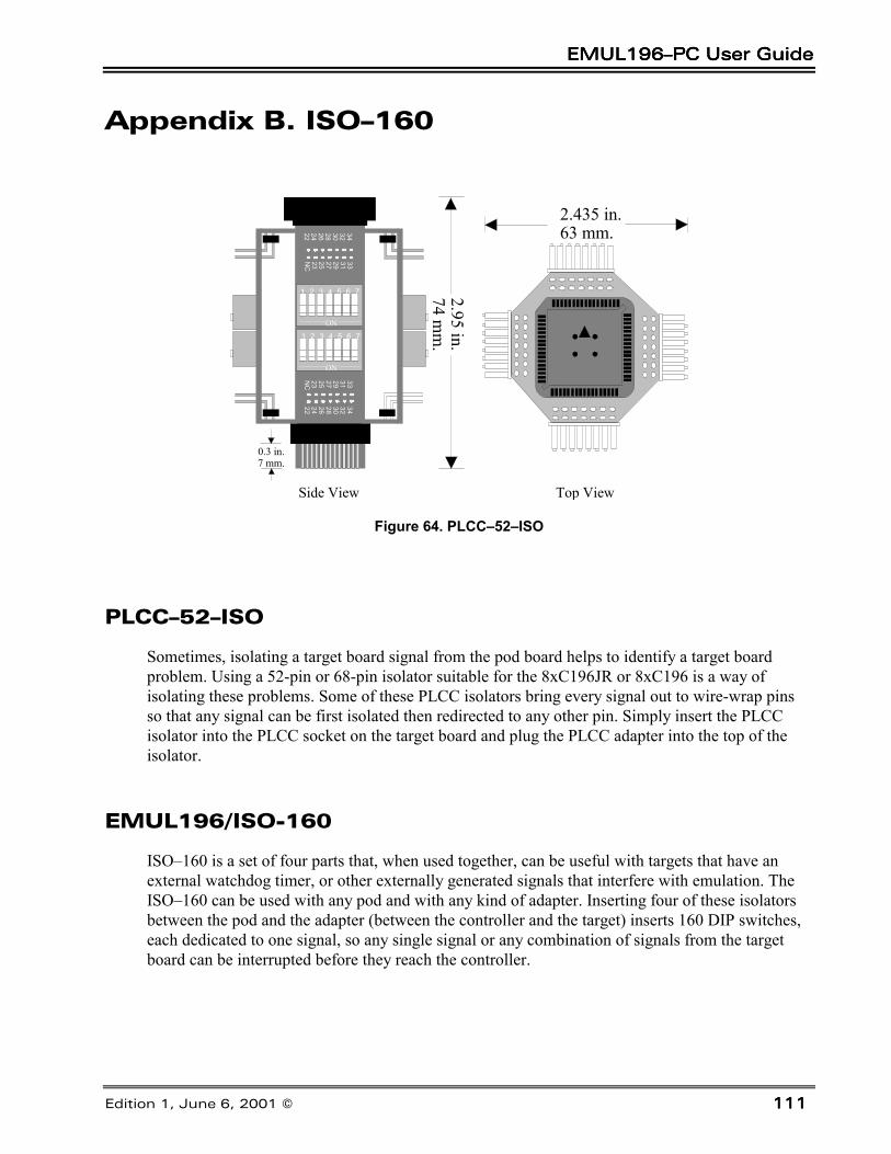
EMUL196–PC User GuideEMUL196–PC User GuideEMUL196–PC User GuideEMUL196–PC User Guide
Edition 1, June 6, 2001 © 111111111
Appendix B. ISO–160
333129272523NC
1 2 3 4 5 6 7
ON
ON
2.95 in.74 m
m.
2.435 in.63 mm.
1 2 3 4 5 6 7
34323028262422
333129272523NC
34323028262422
0.3 in.7 mm.
Side View Top View
Figure 64. PLCC–52–ISO
PLCC–52–ISO
Sometimes, isolating a target board signal from the pod board helps to identify a target boardproblem. Using a 52-pin or 68-pin isolator suitable for the 8xC196JR or 8xC196 is a way ofisolating these problems. Some of these PLCC isolators bring every signal out to wire-wrap pinsso that any signal can be first isolated then redirected to any other pin. Simply insert the PLCCisolator into the PLCC socket on the target board and plug the PLCC adapter into the top of theisolator.
EMUL196/ISO-160
ISO–160 is a set of four parts that, when used together, can be useful with targets that have anexternal watchdog timer, or other externally generated signals that interfere with emulation. TheISO–160 can be used with any pod and with any kind of adapter. Inserting four of these isolatorsbetween the pod and the adapter (between the controller and the target) inserts 160 DIP switches,each dedicated to one signal, so any single signal or any combination of signals from the targetboard can be interrupted before they reach the controller.
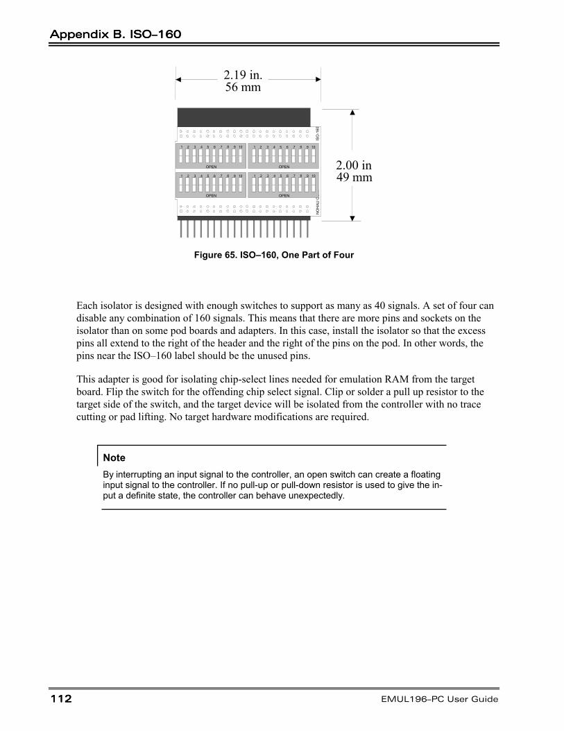
Appendix B. ISO–160Appendix B. ISO–160Appendix B. ISO–160Appendix B. ISO–160
112112112112 EMUL196–PC User Guide
NO
HAU
CO
RP
ISO
-160
21 3 4 5 6 7 8 9 10 21 3 4 5 6 7 8 9 10
21 3 4 5 6 7 8 9 1021 3 4 5 6 7 8 9 10
OPENOPEN
OPEN OPEN
2.19 in.56 mm
2.00 in.49 mm
Figure 65. ISO–160, One Part of Four
Each isolator is designed with enough switches to support as many as 40 signals. A set of four candisable any combination of 160 signals. This means that there are more pins and sockets on theisolator than on some pod boards and adapters. In this case, install the isolator so that the excesspins all extend to the right of the header and the right of the pins on the pod. In other words, thepins near the ISO–160 label should be the unused pins.
This adapter is good for isolating chip-select lines needed for emulation RAM from the targetboard. Flip the switch for the offending chip select signal. Clip or solder a pull up resistor to thetarget side of the switch, and the target device will be isolated from the controller with no tracecutting or pad lifting. No target hardware modifications are required.
NoteBy interrupting an input signal to the controller, an open switch can create a floatinginput signal to the controller. If no pull-up or pull-down resistor is used to give the in-put a definite state, the controller can behave unexpectedly.
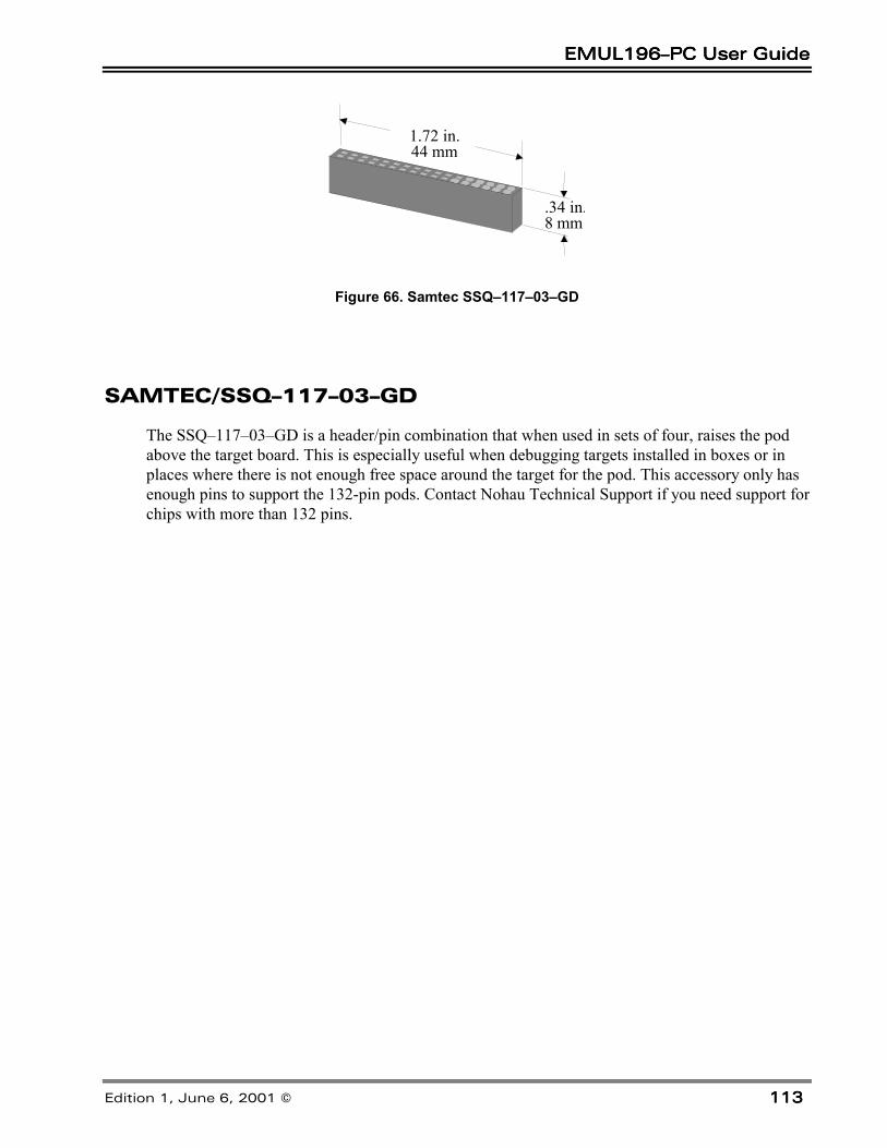
EMUL196–PC User GuideEMUL196–PC User GuideEMUL196–PC User GuideEMUL196–PC User Guide
Edition 1, June 6, 2001 © 113113113
.34 in.8 mm
1.72 in.44 mm
Figure 66. Samtec SSQ–117–03–GD
SAMTEC/SSQ–117–03–GD
The SSQ–117–03–GD is a header/pin combination that when used in sets of four, raises the podabove the target board. This is especially useful when debugging targets installed in boxes or inplaces where there is not enough free space around the target for the pod. This accessory only hasenough pins to support the 132-pin pods. Contact Nohau Technical Support if you need support forchips with more than 132 pins.

Appendix B. ISO–160Appendix B. ISO–160Appendix B. ISO–160Appendix B. ISO–160
114114114114 EMUL196–PC User Guide
EMUL196–PC User GuideEMUL196–PC User GuideEMUL196–PC User GuideEMUL196–PC User Guide
Edition 1, June 6, 2001 © 115115115
Appendix C. Compilers
Overview
In general, the Seehau software will accept a hex file or the absolute file from the linker. Thehex file will contain only hex information in Intel hex format, and not include any symbolicinformation. The absolute file from the linker will contain both the hex information and thesymbolic information.
There are two software packages currently supported by the Seehau 196 software:
• Tasking• IAR.
Refer to the appropriate sections in this guide for specific information.
Tasking
Compiler Notes
Like the assembler, the debug switch produces all the symbols needed by the debugger and putsthem in the unlinked object file. Set all other switches to match your target. For more informationabout other compiler command line settings, refer to the manual from Tasking. If the default isused within the compiler and linker, the output file to be loaded into Seehau 196 will have a .omfextension. This file will contain both the hex and symbolic information.
Assembler Notes
To do source level debugging, add two switches when assembling your code:
• debug• source
NoteThis applies only if you have V4.0, Rev. 3 or later of the Tasking assembler.Previous versions did not support this feature.
A typical command follows:asm196 cstart.asm md(nt) farcode debug source
Set all other switches to match your target. For more information about other assembler settings,refer to the Tasking manual.
Appendix C. CompilersAppendix C. CompilersAppendix C. CompilersAppendix C. Compilers
116116116116 EMUL196–PC User Guide
The example files on the release disk include a file called Cstart.asm. For simplicity, use that fileinstead of any of the startup example files shipped with the compiler when compiling examples.
NoteTo get line number/source information from Tasking V4.0, use the source switch.
IAR
Seehau 196 will only support the hex or UBROF format from this package. The UBROF forma-tion will contain both the hex information and the symbolic information. Other formats should notbe selected, as they will cause problems when trying to view symbols.
EMUL196–PC User GuideEMUL196–PC User GuideEMUL196–PC User GuideEMUL196–PC User Guide
Edition 1, June 6, 2001 © 117117117
Appendix D. Emulator / Trace AddressExamples
Figure 67. Pin Addressing 100 Hex Range
Appendix D. Emulator / Trace Address ExamplesAppendix D. Emulator / Trace Address ExamplesAppendix D. Emulator / Trace Address ExamplesAppendix D. Emulator / Trace Address Examples
118118118118 EMUL196–PC User Guide
Figure 68. Pin Addressing 200 Hex Range
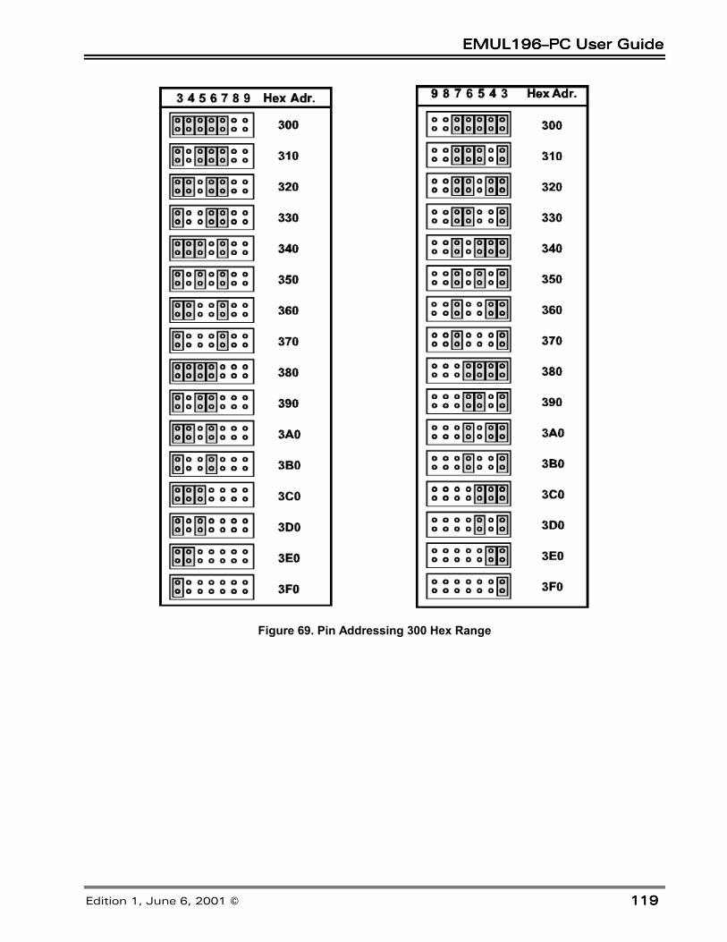
EMUL196–PC User GuideEMUL196–PC User GuideEMUL196–PC User GuideEMUL196–PC User Guide
Edition 1, June 6, 2001 © 119119119
Figure 69. Pin Addressing 300 Hex Range

Appendix D. Emulator / Trace Address ExamplesAppendix D. Emulator / Trace Address ExamplesAppendix D. Emulator / Trace Address ExamplesAppendix D. Emulator / Trace Address Examples
120120120120 EMUL196–PC User Guide
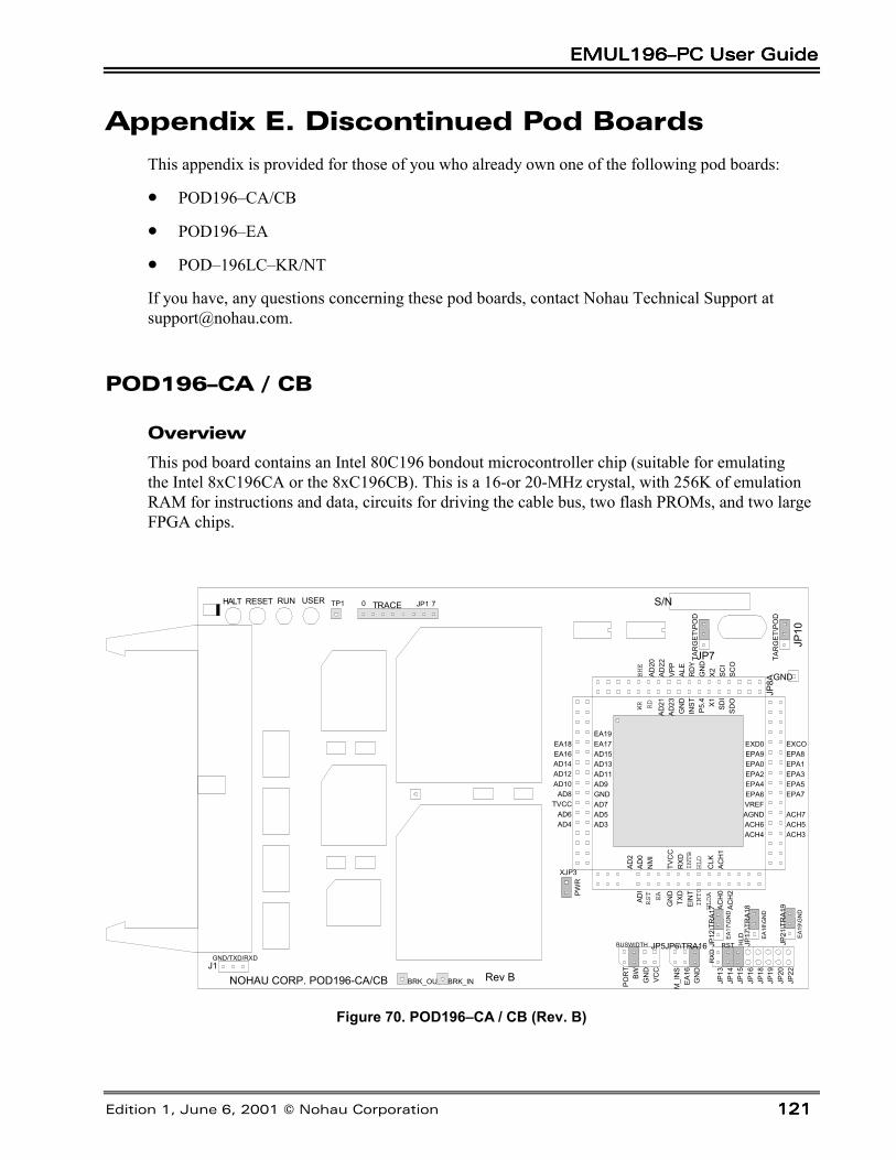
EMUL196–PC User GuideEMUL196–PC User GuideEMUL196–PC User GuideEMUL196–PC User Guide
Edition 1, June 6, 2001 © Nohau Corporation 121121121121
Appendix E. Discontinued Pod Boards
This appendix is provided for those of you who already own one of the following pod boards:
• POD196–CA/CB
• POD196–EA
• POD–196LC–KR/NT
If you have, any questions concerning these pod boards, contact Nohau Technical Support [email protected].
POD196–CA / CB
Overview
This pod board contains an Intel 80C196 bondout microcontroller chip (suitable for emulatingthe Intel 8xC196CA or the 8xC196CB). This is a 16-or 20-MHz crystal, with 256K of emulationRAM for instructions and data, circuits for driving the cable bus, two flash PROMs, and two largeFPGA chips.
NOHAU CORP. POD196-CA/CB
TP1
TAR
GET
\PO
D
JP10
XJP3
PWR
TRACE JP1 S/N
J1
EA19EA17AD15AD13AD11AD9GNDAD7AD5AD3
EA18EA16AD14AD12AD10
AD8TVCC
AD6AD4
AD2
AD0
NM
I
TVC
CR
XDINTB
HLD
CLK
ACH
1
ADI
RST
EA
GN
DTX
DEI
NT
INT0
HLDA
ACH
0AC
H2
JP7BHE
AD20
AD22
VPP
ALE
RD
YG
ND
X2 SCI
SCO
WR RD
AD21
AD23
GN
DIN
STP5
.4 X1 SDI
SDO
GND
JP8A
JP13
JP14
JP15
JP16
JP18
JP19
JP20
JP22
M_I
NS
EA16
GN
D
POR
TBW GN
DVC
C
EA17
\GN
D
EA18
\GN
D
EA19
\GN
D
RST HLD
EXD0EPA9EPA0EPA2EPA4EPA6VREFAGNDACH6ACH4
EXCOEPA8EPA1EPA3EPA5EPA7
ACH7ACH5ACH3
TAR
GET
\PO
D
Rev B
HALT RESET RUN USER 70
GND/TXD/RXD
JP5JP6\TRA16 JP12
\TR
A17
JP17
\TR
A18
JP21
\TR
A19
BUSWIDTH
RXD
BRK_OUT BRK_IN
Figure 70. POD196–CA / CB (Rev. B)
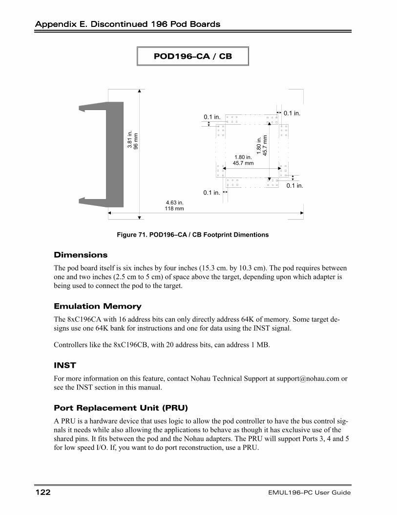
Appendix E. Discontinued 196 Pod BoardsAppendix E. Discontinued 196 Pod BoardsAppendix E. Discontinued 196 Pod BoardsAppendix E. Discontinued 196 Pod Boards
122122122122 EMUL196–PC User Guide
POD196–CA / CB
0.1 in. 0.1 in.
0.1 in.0.1 in.
1.8
0 in
.45
.7 m
m
1.80 in.45.7 mm
3.8
1 in
.96
mm
4.63 in.118 mm
Figure 71. POD196–CA / CB Footprint Dimentions
Dimensions
The pod board itself is six inches by four inches (15.3 cm. by 10.3 cm). The pod requires betweenone and two inches (2.5 cm to 5 cm) of space above the target, depending upon which adapter isbeing used to connect the pod to the target.
Emulation Memory
The 8xC196CA with 16 address bits can only directly address 64K of memory. Some target de-signs use one 64K bank for instructions and one for data using the INST signal.
Controllers like the 8xC196CB, with 20 address bits, can address 1 MB.
INST
For more information on this feature, contact Nohau Technical Support at [email protected] orsee the INST section in this manual.
Port Replacement Unit (PRU)
A PRU is a hardware device that uses logic to allow the pod controller to have the bus control sig-nals it needs while also allowing the applications to behave as though it has exclusive use of theshared pins. It fits between the pod and the Nohau adapters. The PRU will support Ports 3, 4 and 5for low speed I/O. If, you want to do port reconstruction, use a PRU.
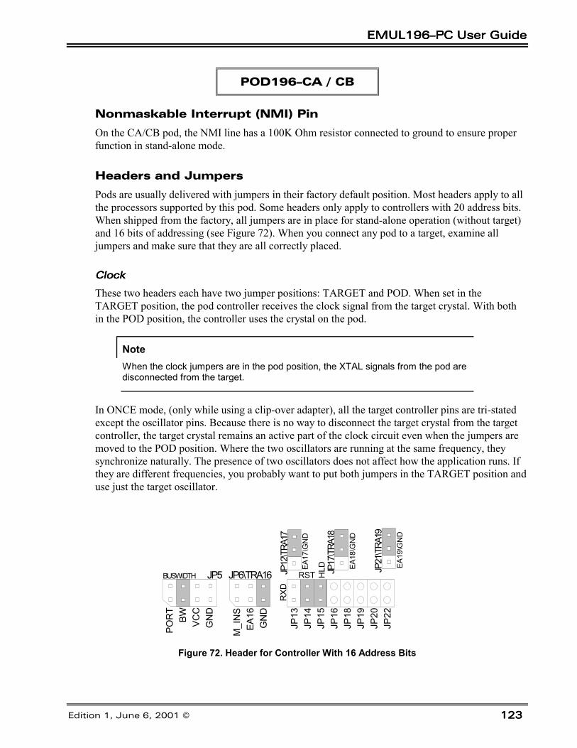
EMUL196–PC User GuideEMUL196–PC User GuideEMUL196–PC User GuideEMUL196–PC User Guide
Edition 1, June 6, 2001 © 123123123
POD196–CA / CB
Nonmaskable Interrupt (NMI) Pin
On the CA/CB pod, the NMI line has a 100K Ohm resistor connected to ground to ensure properfunction in stand-alone mode.
Headers and Jumpers
Pods are usually delivered with jumpers in their factory default position. Most headers apply to allthe processors supported by this pod. Some headers only apply to controllers with 20 address bits.When shipped from the factory, all jumpers are in place for stand-alone operation (without target)and 16 bits of addressing (see Figure 72). When you connect any pod to a target, examine alljumpers and make sure that they are all correctly placed.
ClockClockClockClock
These two headers each have two jumper positions: TARGET and POD. When set in theTARGET position, the pod controller receives the clock signal from the target crystal. With bothin the POD position, the controller uses the crystal on the pod.
NoteWhen the clock jumpers are in the pod position, the XTAL signals from the pod aredisconnected from the target.
In ONCE mode, (only while using a clip-over adapter), all the target controller pins are tri-statedexcept the oscillator pins. Because there is no way to disconnect the target crystal from the targetcontroller, the target crystal remains an active part of the clock circuit even when the jumpers aremoved to the POD position. Where the two oscillators are running at the same frequency, theysynchronize naturally. The presence of two oscillators does not affect how the application runs. Ifthey are different frequencies, you probably want to put both jumpers in the TARGET position anduse just the target oscillator.
JP13
JP14
JP15
JP16
JP18
JP19
JP20
JP22
M_I
NS
EA16
GN
D
POR
TBW VC
CG
ND
EA17
\GN
D
EA18
\GN
D
EA19
\GN
D
RST HLDJP5 JP6\TRA16 JP
12\T
RA17
JP17
\TRA
18
JP21
\TRA
19
BUSWIDTH
RXD
Figure 72. Header for Controller With 16 Address Bits
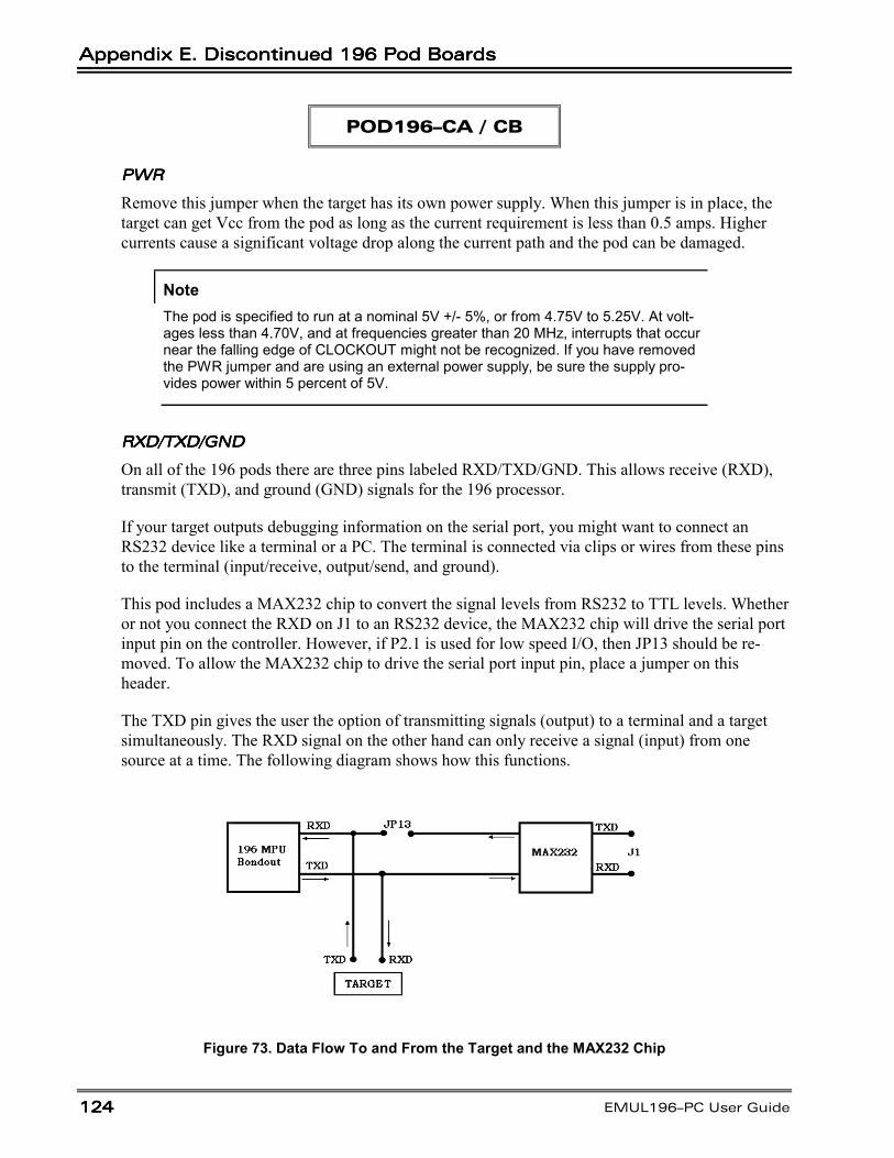
Appendix E. Discontinued 196 Pod BoardsAppendix E. Discontinued 196 Pod BoardsAppendix E. Discontinued 196 Pod BoardsAppendix E. Discontinued 196 Pod Boards
124124124124 EMUL196–PC User Guide
POD196–CA / CB
PWRPWRPWRPWR
Remove this jumper when the target has its own power supply. When this jumper is in place, thetarget can get Vcc from the pod as long as the current requirement is less than 0.5 amps. Highercurrents cause a significant voltage drop along the current path and the pod can be damaged.
NoteThe pod is specified to run at a nominal 5V +/- 5%, or from 4.75V to 5.25V. At volt-ages less than 4.70V, and at frequencies greater than 20 MHz, interrupts that occurnear the falling edge of CLOCKOUT might not be recognized. If you have removedthe PWR jumper and are using an external power supply, be sure the supply pro-vides power within 5 percent of 5V.
RXD/TXD/GNDRXD/TXD/GNDRXD/TXD/GNDRXD/TXD/GND
On all of the 196 pods there are three pins labeled RXD/TXD/GND. This allows receive (RXD),transmit (TXD), and ground (GND) signals for the 196 processor.
If your target outputs debugging information on the serial port, you might want to connect anRS232 device like a terminal or a PC. The terminal is connected via clips or wires from these pinsto the terminal (input/receive, output/send, and ground).
This pod includes a MAX232 chip to convert the signal levels from RS232 to TTL levels. Whetheror not you connect the RXD on J1 to an RS232 device, the MAX232 chip will drive the serial portinput pin on the controller. However, if P2.1 is used for low speed I/O, then JP13 should be re-moved. To allow the MAX232 chip to drive the serial port input pin, place a jumper on thisheader.
The TXD pin gives the user the option of transmitting signals (output) to a terminal and a targetsimultaneously. The RXD signal on the other hand can only receive a signal (input) from onesource at a time. The following diagram shows how this functions.
Figure 73. Data Flow To and From the Target and the MAX232 Chip
EMUL196–PC User GuideEMUL196–PC User GuideEMUL196–PC User GuideEMUL196–PC User Guide
Edition 1, June 6, 2001 © 125125125
POD196–CA / CB
WARNING
The processor cannot handle input from two different sources at the same time. If you are con-nected to a terminal, through the MAX232 chip you must be in stand-alone mode (not connected toa target). If you are connected to a target, the RXD jumper on JP13 must be removed, so you arenot connected to a terminal and a target at the same time.
RSTRSTRSTRST
Occasionally, a target might contain an external device designed to reset the controller by pullingthe /RST pin low (i.e., a watchdog timer). The signal from the target /RST pin passes throughthe RST header. Removing the RST jumper prevents the external device from resetting the podcontroller.
HLDHLDHLDHLD
The target /HLD signal passes through the HLD header. Removing this jumper will prevent thepod controller from receiving the Hold Request from a target device.
BUSWIDTHBUSWIDTHBUSWIDTHBUSWIDTH
This header controls the signal sent to the FLEX logic chips. The bondout chip does not correctlyassert the bus control signals when the CCBs are set to have an 8-bit wide bus. If you need toemulate an 8-bit bus, you can do so reliably by setting the CCBs to have a dynamic buswidth andadding a jumper to this header in the GND position. Have two jumpers on this header, one in theBW position and one in the GND position.
NoteThe pair of pins on the BUSWIDTH header with the PORT label is reserved for afeature not yet implemented. Do not place the jumper on this pair of pins.
WARNING
Whether you pull the BW pin high or low, make sure that the jumper settings agree with your targethardware design. If they are different, you can damage the pod, the target, or both. It is recom-mended that you leave the Vcc and GND jumpers off when you are plugged into the target. Thiswill allow the target to control the BW pin.
Appendix E. Discontinued 196 Pod BoardsAppendix E. Discontinued 196 Pod BoardsAppendix E. Discontinued 196 Pod BoardsAppendix E. Discontinued 196 Pod Boards
126126126126 EMUL196–PC User Guide
POD196–CA / CB
EA16-EA19EA16-EA19EA16-EA19EA16-EA19
The jumpers on these headers must remain in their default or grounded positions for all controllersthat use 16 address bits. Controllers like the 8xC196CB have 20 address bits and you will likelyneed to change these jumpers.
Each of these jumpers sits between the controller and the address signals going to the emulator andtrace boards. These address signals are used to correctly locate write cycles in Shadow RAM andtrace records of all kinds in the trace buffer.
If your application uses a controller with 20 address bits, for every address bit above 15 that theapplication uses for addressing, move the corresponding jumper from the GND position to theEA1x position. This will pass that address signal on to the emulator and trace boards. For eachof the bits that are used for I/O instead of addressing, put the jumper on the GND side. This also,applies to JP/TRA16 although it has a different geometry than the other headers.
WARNING
Do not put more than one jumper on EA16, also labeled JP6. Having two jumpers on this headercan damage the bondout controller or some other part of the pod.
87C196CB Bondout Errata
PRU with /#EA Pin HighPRU with /#EA Pin HighPRU with /#EA Pin HighPRU with /#EA Pin HighThe POD196–256–CA/CB, Rev. B, in a limited way, supports single chip customers using thePRU with the /#EA pin high. The CA device has a 32K internal EPROM/OTP. The CB devicehas a 56K internal EPROM/OTP. The POD196–256–CA/CB, Rev. B uses the 8xC196CB bond-out chip which has 48K, resulting in the following restrictions when using a PRU:
• CA device users cannot access external peripherals between A000 and DFFF with the PRUattached.
• CB device users cannot correctly support 56K-code emulation in single chip mode. Therefore,if code executes between E000 and FFFF or FE000 and FFFFF, accesses will go external andcorrupt the low speed I/O pins used on Port 3 and Port 4.
Extended Addressing BugsExtended Addressing BugsExtended Addressing BugsExtended Addressing Bugs
The POD196–256–CA/CB, Rev. B 8xC196CB bondout has a number of extended addressingbugs. These bugs do not appear on the 87C196CB component. They will be fixed on a subsequentstepping of the 8xC196CB-bondout silicon. Therefore, the 87C196CB emulator will behave dif-ferently than the 87C196CB component. Following is a list of these bugs and their suggested soft-ware workarounds:
EMUL196–PC User GuideEMUL196–PC User GuideEMUL196–PC User GuideEMUL196–PC User Guide
Edition 1, June 6, 2001 © 127127127
POD196–CA / CB
• EST/ELD Base-Indexed Addressing Mode Bug
• EST/ELD Indirect Addressing Mode Bug
• Aborted Interrupt Vectors to Lowest Priority Bug
• PTS Request During Interrupt latency Bug
• ILLEGAL Opcode Interrupt Vector Bug
• SJMP/Conditional Jumps Near Page Boundary
• EBR Dummy Prefetch Anomaly
The following section explains in detail the above noted workarounds:
BUG 1:EST/ELD Base-Indexed Addressing Mode
When executing from external memory, the EST/ELD instructions in base-indexed addressingmode do not access the correct memory locations.
The following text explains how extended base-indexed addressing should work:ELD destination_16bit, base_address_24bit [index_32bit]
After the above instruction is executed, the destination register contains the data at the effectiveaddress.destination_16bit <= [base_address24bit+index_32bit]
Note [ ] => the contents of
The effective address is calculated by the MICROCODE engine within the device.effective_address = base_address + index
An example of an extended base-indexed load instruction is shown below, let:
Register 20H = 0000 0002H (32 bit value)
Register 1CH = 000H (16-bit value)
The word at location 000602H contains 1234H
The word at location 020602H contains 5678H
ELD 1CH,000600H[20H] ; executing from somewhere in ; EXTERNAL MEMORY
Appendix E. Discontinued 196 Pod BoardsAppendix E. Discontinued 196 Pod BoardsAppendix E. Discontinued 196 Pod BoardsAppendix E. Discontinued 196 Pod Boards
128128128128 EMUL196–PC User Guide
POD196–CA / CB
The base address 000600H is added to the 32-bit register 20H to obtain the effective address, so:
Equation 1: Effective Address CalculationsBase address 000600H term ARegister 20H +00000002H term B
000602H
Therefore:
1CH should contain the value at location 000602H1CH should contain 1234H
However, with the 8xC196CB bondout, register 1CH contains 5678H after the above instruction isexecuted. 1CH is being loaded with the value at location 020602H.
Therefore, the 8xC196CB bondout is performing the add incorrectly (see Equation 1). The 24-bitadd is limited by the 16-bit internal buswidth. Since the internal bus is 16 bits wide, two adds needto be done to achieve a 24-bit add. When the first add is done:
Base address 0600H term ARegister 20H 0002H term B
0602H
Term B is left on the bus for the second 16-bit add, so:
Base address 00H term ARegister 20H 0002H term B (left over from first add)
02H
The incorrect calculation leads to an incorrect effective address: 020602H.
A: Assembly Language WorkaroundIf programming in assembly language, be aware of the bug and avoid using the extended base-indexed instruction. One workaround would be to replace the following extended base-indexedinstruction:ELD 1CH, 000600H [20H]
EMUL196–PC User GuideEMUL196–PC User GuideEMUL196–PC User GuideEMUL196–PC User Guide
Edition 1, June 6, 2001 © 129129129
POD196–CA / CB
With the following:;**************************************************************rseg at 20Heffective_address: dsl 1 ; 32-bit long word registerbase_address: dsl 1 ; 32-bit long word registerindex: dsl 1 ; 32-bit long word register
; only 24 bits needed for; address
clr effective_address ; zero out long wordsclr effective_address+2clr base_addressclr base_address+2clr indexclr index+2add effective_address, base_address, index
; add lower words of index; and base address
addcb effective_address+2, index+2; add upper byte from index to; upper byte of effective; address resulting in a 24-bit; add
ELD 1CH, [effective_address] ; straight indirect addressing; works correctly
;**************************************************************
B: C Compiler Workarounds
Recommendation 1: Limit Data Space to 64K
The bug can be avoided if you declare all data access to be within page 00H (64K page). This canbe accomplished with the C compiler directive called NEAR. At the top of the C source code,place the following directives:#PRAGMA FARCODE#PRAGMA NEARDATA
The FARCODE directive tells the compiler to use extended branching instructions (i.e. ECALL,EJMP) to reference any address within the 1-MB space. The NEARDATA directive tells the com-piler that ALL data references will be within page 00H (000000H – 00FFFFH). Hence, the com-piler will just use the nonextended load and store instructions (i.e. LD, ST).
Disadvantage
This (NEARDATA) limits any access to page 00H. Therefore, the user will only have 64K of dataspace. However, program space can extend the entire 1-MB of address space (FARCODE).
Appendix E. Discontinued 196 Pod BoardsAppendix E. Discontinued 196 Pod BoardsAppendix E. Discontinued 196 Pod BoardsAppendix E. Discontinued 196 Pod Boards
130130130130 EMUL196–PC User Guide
POD196–CA / CB
Recommendation 2: Limit Code Space to 9 INTERNAL Memory
Limit code accesses to just the internal (EP) ROM (page FFH). The bug does not exist when exe-cuting from internal memory. The C compiler directives are:#PRAGMA NEARCODE#PRAGMA FARDATA
The NEARCODE directive tells the compiler that all code branches will reside within page FFH(FF0000H – FFFFFFH). The FARDATA directive tells the compiler that data accesses can beanywhere within the 1-MB address space. Therefore, the compiler will use extended load and storeinstructions. (But the extended base-indexed instruction will work since all the code is executinginternally.)
Disadvantage
Code, which accesses FARDATA, is limited to 32K (internal EPROM size). Glossary ofC Compiler Terms:
• NEAR—constraints, data or code within page 00H (000000H through 00FFFFH). Examples:NEARCONST, NEARDATA, and NEARCODE
• FAR—constants, data or code that lie anywhere within 1-MB address range (000000Hthrough FFFFFFH)
BUG 2: EST/ELD Indirect Addressing Mode
The ELD/EST instructions in indirect addressing with auto-increment mode do not increment overthe 64K page. This bug does not exist on the CB silicon.
Example
;************************************************************** ld temp,#0FFFCH ld temp+2,#02H; upper word equal to 0002H eld value,[temp]+; after this instruction ; temp=0002FFFEH eld value, [temp]+; after this instruction ; temp=00030000H end;**************************************************************
Temp should contain 00030000H after the last auto-increment statement.
ERROR
Instead, temp contains 03020000H after the last auto-increment statement. Therefore, the bug isthat the upper byte in the 32-bit long word is being loaded with the incremented 64K page value(03H in this case). What should happen is that the lower word rolls over to 0000H (as it does). Inaddition, the upper word should increment to 0003H (as it does).
EMUL196–PC User GuideEMUL196–PC User GuideEMUL196–PC User GuideEMUL196–PC User Guide
Edition 1, June 6, 2001 © 131131131
POD196–CA / CB
Workaround
The workaround for this auto-increment bug is to do the incrementing with ADD and ADDCstatements on the index register (in this case, temp). To fix the code above, use the followingworkaround code:
;********************************************************************* ld temp,#0FFFF\CH ld temp+2,#0002H eld lch, [temp] ; get word from 0002FFFCH add temp,#2 ; increment by 1 addc temp+2#0 ; add in carry to the upper
; word or page value eld lch, [temp] ; get word from 0002FFFEH add temp,#1 addc temp+2,#0 eld lch, [temp] ; get word from 00030000H;*********************************************************************
BUG 3: Aborted Interrupt Vectors to Lowest Priority
In 24-bit mode, if an interrupt is aborted either intentionally or unintentionally, an undesiredbranch to the lowest priority interrupt vector (FF2000H) can occur even if the lowest priority inter-rupt is not enabled. This can occur if any bit in the INT_MASK, INT_MASK1, INT_PEND, orINT_PEND1 register is cleared after the corresponding INT_PEND or INT_PEND1 bit is set.
Example
If the EXTINT0 interrupt is enabled by setting INT_MASK3, and a rising edge on EXTINT0 oc-curs \,INT_PEND.3 is set. The following instruction might cause the CPU to vector to 0FF2000Hinstead of 0FF2006H.ANDB INT_MASK,#0F7H; masks EXTINT0
Workaround
If a disable interrupt (DI) instruction is used prior to clearing a bit in the INT_MASK,INT_MASK1, INT_PEND, or INT_PEND1, the problem will be avoided. The following code ex-ample demonstrates how to safely disable the EXTINT0 interrupt.DIANDB INT_MASK, #0F7HEI
An undesired branch to the lowest priority interrupt can occur if an interrupt is aborted, unless theworkaround is used.
Appendix E. Discontinued 196 Pod BoardsAppendix E. Discontinued 196 Pod BoardsAppendix E. Discontinued 196 Pod BoardsAppendix E. Discontinued 196 Pod Boards
132132132132 EMUL196–PC User Guide
POD196–CA / CB
BUG 4: PTS Request During interrupt Latency
In 24-bit mode, if a standard interrupt occurs at approximately the same time as a PTS servicedinterrupt, the PTS interrupt can be processed as a standard interrupt. The standard interrupt serviceroutine for PTS serviced interrupt (usually referred to as the End-of-PTS) is typically used tomodify the PTS control block and enable the PTS by setting the corresponding bit in the PTSSELregister. When this occurs, the End-of-PTS service routine will execute regardless of the value inPTSCOUNT. Therefore, an undetermined number of PTS cycles will not occur. This bug appliesto all interrupts serviced by the PTS.
Workaround
In the standard interrupt service routine (End-of-PTS) for each PTS enabled, the first instructionfollowing a PUSHA should determine if the associated bit in the PTSSEL register is set orcleared. Checking this bit will determine if the desired number of cycles were completed or a pre-mature End-of-PTS occurred. If the bit is set, the associated pending bit in the INT_PEND orINT_PEND1 should be set followed by a RET statement. This will cause a PTS cycle to occur. Ifthe associated bit in the PTSSEL register is cleared, the normal End-of-PTS procedure should beexecuted. The following is an example of a End-of-PTS service routine for the External Interrupt 0(EXTINT0).CSEG AT 0FF2006HDCW EXTINT0_END_OF_PTS
BUG 5: ILLEGAL Opcode Interrupt Vector
The ILLEGAL opcode interrupt should be generated when there is an attempt to execute an unde-fined opcode in the 196 core and should vector to address FF2012H to handle the interrupt. How-ever, in 24-bit mode, the vector address for the illegal opcode interrupt will not be generatedcorrectly, and a random vector address will be generated.
Workaround
Use a C-compiler or assembler that will flag the ILLEGAL opcode or put a RESET opcode, FFH,at the end of any data tables or unused memory locations.
There are only two ILLEGAL opcodes (10H and E5H) out of 256 opcodes. So if your codeaccidentally jumps into a data table, there is only a 0.8 per cent chance that one of the twoillegal opcodes will be found.
BUG 6: SJMP / Conditional Jumps Near Page Boundary
In 24-bit mode, the execution of a SJMP instruction with a negative offset occurring near a pageboundary will result in the device jumping to an incorrect page address. The upper bits of theaddress are corrupted during the jump and will contain the address of the preceding page. Thisbehavior is also exhibited during the execution of conditional jump instructions.
EMUL196–PC User GuideEMUL196–PC User GuideEMUL196–PC User GuideEMUL196–PC User Guide
Edition 1, June 6, 2001 © 133133133
POD196–CA / CB
Software Workaround
This described behavior of the SJMP and Conditional Jump instructions occurs only in 24-bitmode when the specific instruction is executed near a page boundary. In order to prevent this be-havior, the programmer must insure that these instructions are not executed near a page boundary.This can be accomplished by placing several NOP instructions at the top of all 64K pages, whichare used for code execution.
BUG 6: Extended Branch Indirect (EBR) Dummy Prefetch Anomaly
In 24-bit mode, the execution of an EBR instruction near a page boundary will result in an extracode prefetch to a dummy address. This extra prefetch can occur anywhere within the next page.Since this additional prefetch occurs when the Instruction Queue (IQ) is being flushed, the pre-fetched code is not loaded into the IQ registers, and therefore is not executed. Currently, no plansexist to fix this anomaly.
Software Workaround
This described behavior of the EBR instruction only occurs when the EBR instruction occurs neara page boundary. To prevent this behavior, the programmer must ensure the EBR instruction doesnot occur near a page boundary. This can be accomplished by placing several NOP instructions atthe top of all 64K pages, which are used for code execution.
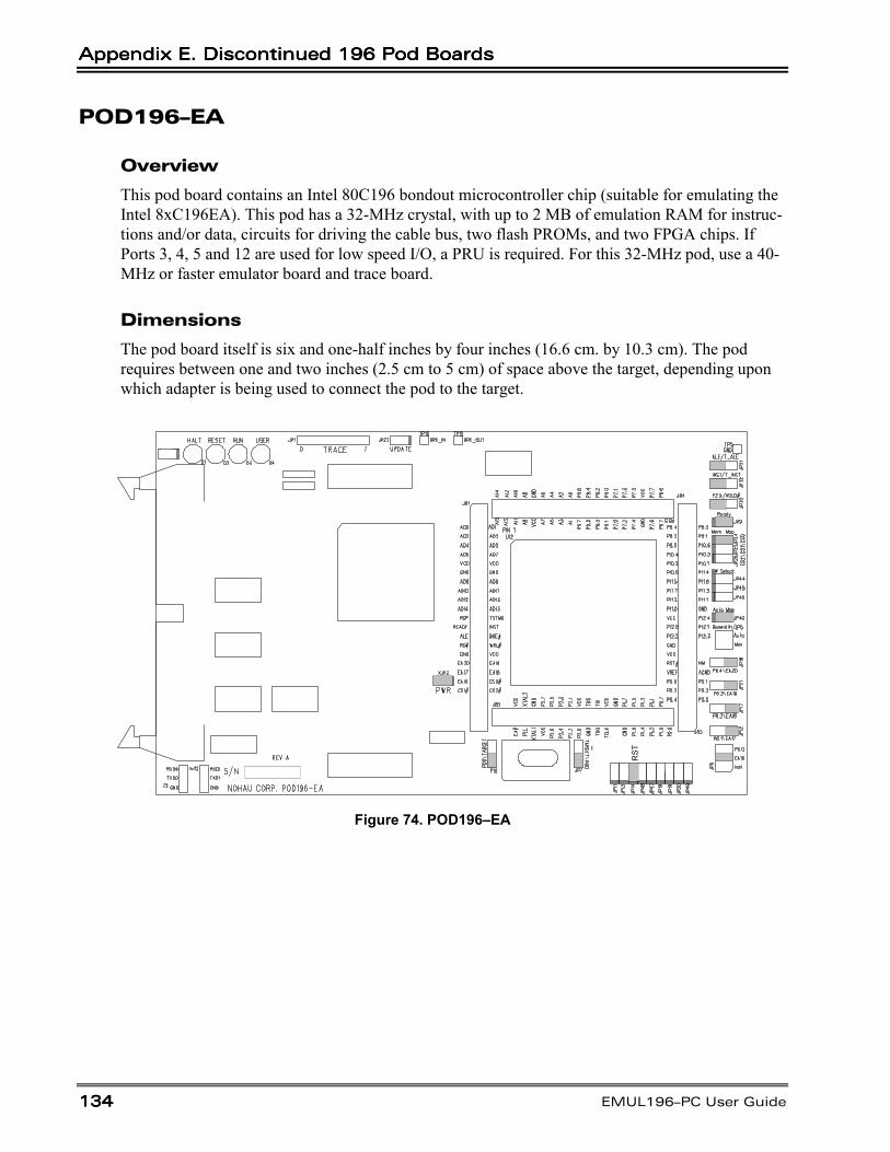
Appendix E. Discontinued 196 Pod BoardsAppendix E. Discontinued 196 Pod BoardsAppendix E. Discontinued 196 Pod BoardsAppendix E. Discontinued 196 Pod Boards
134134134134 EMUL196–PC User Guide
POD196–EA
Overview
This pod board contains an Intel 80C196 bondout microcontroller chip (suitable for emulating theIntel 8xC196EA). This pod has a 32-MHz crystal, with up to 2 MB of emulation RAM for instruc-tions and/or data, circuits for driving the cable bus, two flash PROMs, and two FPGA chips. IfPorts 3, 4, 5 and 12 are used for low speed I/O, a PRU is required. For this 32-MHz pod, use a 40-MHz or faster emulator board and trace board.
Dimensions
The pod board itself is six and one-half inches by four inches (16.6 cm. by 10.3 cm). The podrequires between one and two inches (2.5 cm to 5 cm) of space above the target, depending uponwhich adapter is being used to connect the pod to the target.
RS
T
Figure 74. POD196–EA
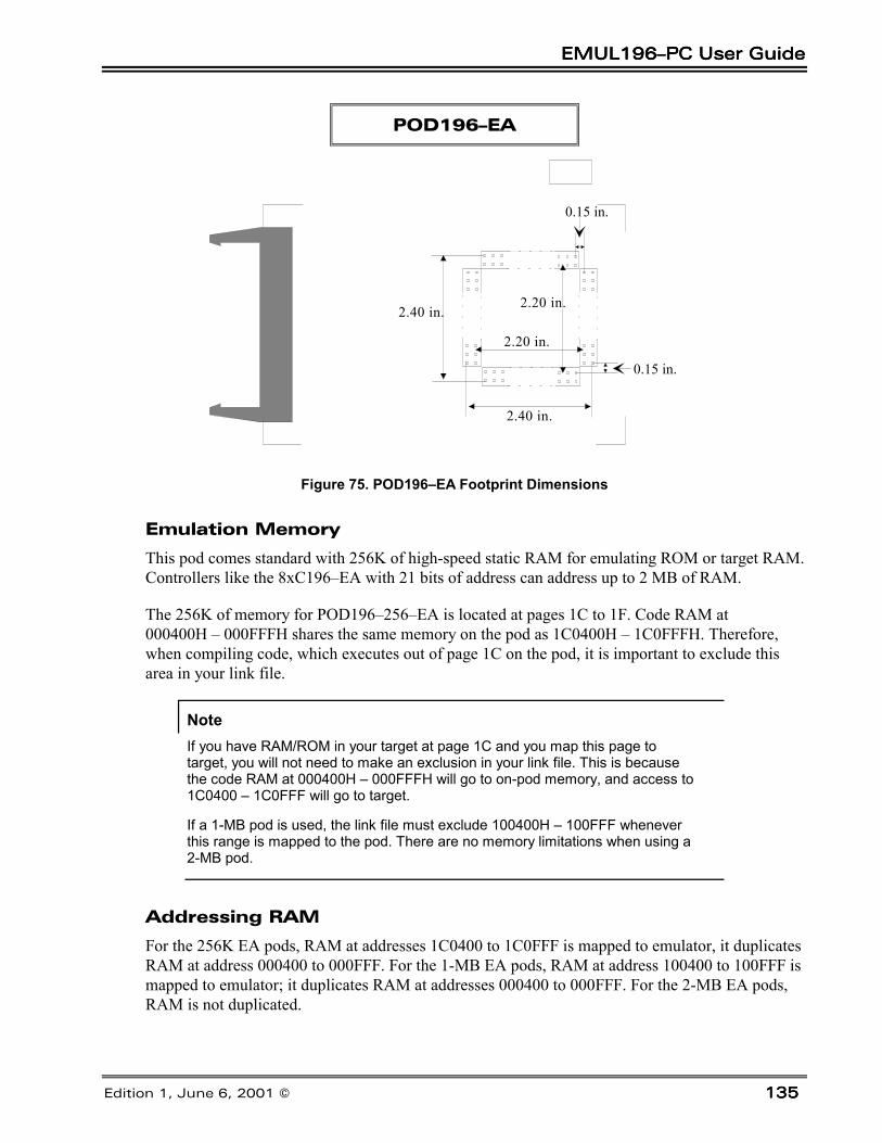
EMUL196–PC User GuideEMUL196–PC User GuideEMUL196–PC User GuideEMUL196–PC User Guide
Edition 1, June 6, 2001 © 135135135
POD196–EA
0.15 in.
2.20 in.
2.40 in.
2.40 in.2.20 in.
0.15 in.
Figure 75. POD196–EA Footprint Dimensions
Emulation Memory
This pod comes standard with 256K of high-speed static RAM for emulating ROM or target RAM.Controllers like the 8xC196–EA with 21 bits of address can address up to 2 MB of RAM.
The 256K of memory for POD196–256–EA is located at pages 1C to 1F. Code RAM at000400H – 000FFFH shares the same memory on the pod as 1C0400H – 1C0FFFH. Therefore,when compiling code, which executes out of page 1C on the pod, it is important to exclude thisarea in your link file.
NoteIf you have RAM/ROM in your target at page 1C and you map this page totarget, you will not need to make an exclusion in your link file. This is becausethe code RAM at 000400H – 000FFFH will go to on-pod memory, and access to1C0400 – 1C0FFF will go to target.
If a 1-MB pod is used, the link file must exclude 100400H – 100FFF wheneverthis range is mapped to the pod. There are no memory limitations when using a2-MB pod.
Addressing RAM
For the 256K EA pods, RAM at addresses 1C0400 to 1C0FFF is mapped to emulator, it duplicatesRAM at address 000400 to 000FFF. For the 1-MB EA pods, RAM at address 100400 to 100FFF ismapped to emulator; it duplicates RAM at addresses 000400 to 000FFF. For the 2-MB EA pods,RAM is not duplicated.
Appendix E. Discontinued 196 Pod BoardsAppendix E. Discontinued 196 Pod BoardsAppendix E. Discontinued 196 Pod BoardsAppendix E. Discontinued 196 Pod Boards
136136136136 EMUL196–PC User Guide
POD196–EA
8-Bit Mode and BHE Mode
If your target is 8-bit, it is required that the WRH/BHE pin be configured as BHE mode. Not doingso will cause the emulator to fail.
Headers and Jumpers
Pod boards are usually delivered with jumpers in their factory default position. Most headers applyto all the processors supported by this pod. When shipped from the factory, all jumpers are inplace for stand-alone operation. When you connect any pod to a target, examine all jumpers andmake sure that they are all correctly placed.
Clock Jumper (JP7, JP10)Clock Jumper (JP7, JP10)Clock Jumper (JP7, JP10)Clock Jumper (JP7, JP10)
These two headers each have two jumper positions: TARGET and POD. They must be moved as apair. When set in the TARGET position, the pod controller receives the clock signal from the tar-get crystal. With both in the POD position, the controller uses the crystal on the pod.
NoteWhen these jumpers are in the POD position, the XTAL signals from the pod arecompletely disconnected from the target.
PLLEN (JP47)PLLEN (JP47)PLLEN (JP47)PLLEN (JP47)
Install this jumper to connect target PLLEN to the bondout. The default position is with JP47installed.
Code RAM (JP49)Code RAM (JP49)Code RAM (JP49)Code RAM (JP49)
The 196–EA chip has a separate Vcc pin used to power the internal code RAM. Pin 66 is poweredby the user’s target supply. If the target supply is turned off, then the internal code RAM will belost unless Pin 66 remains at +5V. This jumper should only be installed if you have not consideredthis and plan to perform a power down/up sequence. The default position is with JP49 removed.
PWRPWRPWRPWR
Remove this jumper when the target has its own power supply. When this jumper is in place, thetarget can get Vcc from the pod, which can supply up to 0.5 amps. Higher currents cause a signifi-cant voltage drop along the current path and the pod can be damaged.
EMUL196–PC User GuideEMUL196–PC User GuideEMUL196–PC User GuideEMUL196–PC User Guide
Edition 1, June 6, 2001 © 137137137
POD196–EA
NoteThe pod is specified to run at a nominal 5V +/- 5%, or from 4.75V to 5.25V. At volt-ages less than 4.7V, and at frequencies greater than 16 MHz, interrupts that occurnear the falling edge of CLOCKOUT might not be recognized. If you have removedthe PWR jumper and are using an external power supply, be sure the supply pro-vides power within 5 percent of 5V.
RXD/TXD/GND (JP11 for RXD0 and JP13 for RXD1)RXD/TXD/GND (JP11 for RXD0 and JP13 for RXD1)RXD/TXD/GND (JP11 for RXD0 and JP13 for RXD1)RXD/TXD/GND (JP11 for RXD0 and JP13 for RXD1)
On all of the 196 pods except POD196–EA, there are three pins labeled RXD/TXD/GND.POD196–EA has six pins (RXD0/TXD0/GND0, and RXD1/TXD1/GND1). This allows receive(RXD), transmit (TXD), and ground (GND) signals for the 196 processor.
If your target outputs debugging information on the serial port, you might want to connect anRS232 device like a terminal or a PC. The terminal is connected via clips or wires from these pinsto the terminal (input, output, and ground).
This pod includes a MAX232 chip to convert the signal levels from RS232 to TTL levels. Whetheror not you connect the RXD on J1 and J2 to an RS232 device, the MAX232 chip will drive the se-rial port input pin on the controller. However, if P2.1 and P2.4 are used for low speed I/O, thenJP11 and JP13 should be removed. To allow the MAX232 chip to drive the serial port input pin,place a jumper on theses headers.
The TXD pin gives the user the option of transmitting signals (output) to a terminal and a targetsimultaneously. The RXD signal on the other hand can only receive a signal (input) from onesource at a time. The following diagram shows how this functions.
WARNING
The processor cannot handle input from two different sources at the same time. If you are con-nected to a terminal, through the MAX232 chip you must be in stand-alone mode (not connected toa target). If you are connected to a target the RXD jumper on JP13 must be removed, so you arenot connected to a terminal and a target at the same time.
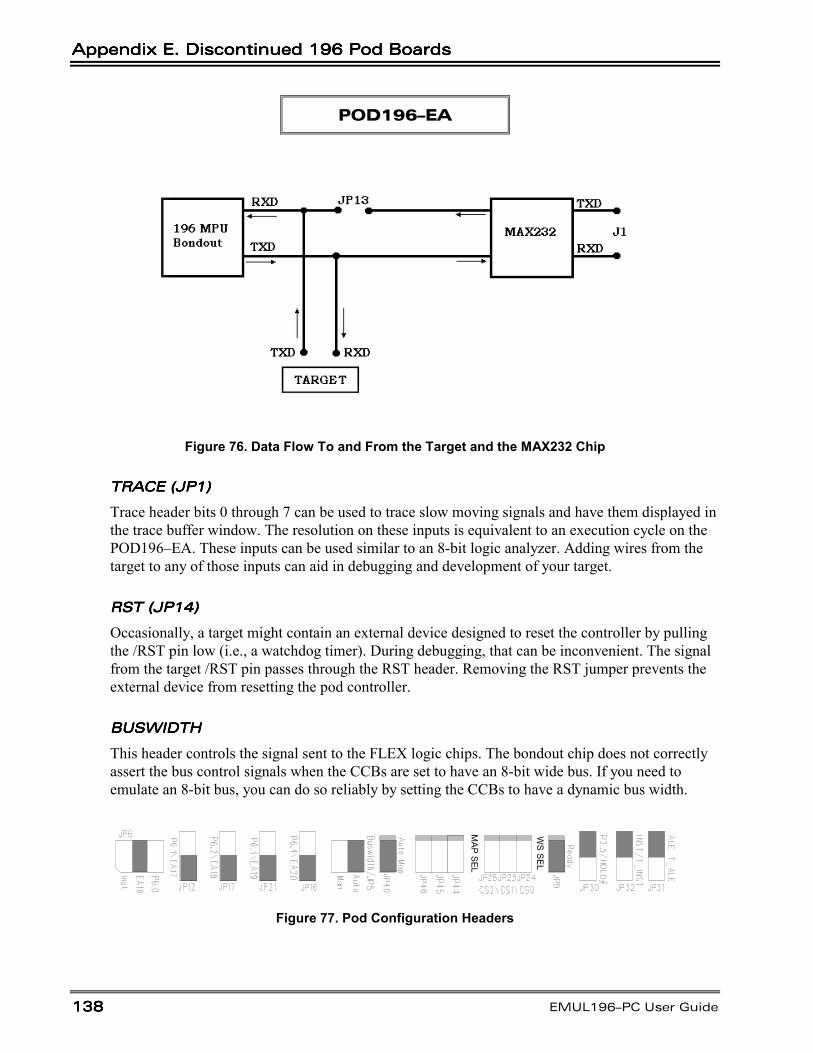
Appendix E. Discontinued 196 Pod BoardsAppendix E. Discontinued 196 Pod BoardsAppendix E. Discontinued 196 Pod BoardsAppendix E. Discontinued 196 Pod Boards
138138138138 EMUL196–PC User Guide
POD196–EA
Figure 76. Data Flow To and From the Target and the MAX232 Chip
TRACE (JP1)TRACE (JP1)TRACE (JP1)TRACE (JP1)
Trace header bits 0 through 7 can be used to trace slow moving signals and have them displayed inthe trace buffer window. The resolution on these inputs is equivalent to an execution cycle on thePOD196–EA. These inputs can be used similar to an 8-bit logic analyzer. Adding wires from thetarget to any of those inputs can aid in debugging and development of your target.
RST (JP14)RST (JP14)RST (JP14)RST (JP14)
Occasionally, a target might contain an external device designed to reset the controller by pullingthe /RST pin low (i.e., a watchdog timer). During debugging, that can be inconvenient. The signalfrom the target /RST pin passes through the RST header. Removing the RST jumper prevents theexternal device from resetting the pod controller.
BUSWIDTHBUSWIDTHBUSWIDTHBUSWIDTH
This header controls the signal sent to the FLEX logic chips. The bondout chip does not correctlyassert the bus control signals when the CCBs are set to have an 8-bit wide bus. If you need toemulate an 8-bit bus, you can do so reliably by setting the CCBs to have a dynamic bus width.
WS SEL
MAP SEL
Figure 77. Pod Configuration Headers
EMUL196–PC User GuideEMUL196–PC User GuideEMUL196–PC User GuideEMUL196–PC User Guide
Edition 1, June 6, 2001 © 139139139
POD196–EA
MAP SEL (JP44, JP45, JP46)MAP SEL (JP44, JP45, JP46)MAP SEL (JP44, JP45, JP46)MAP SEL (JP44, JP45, JP46)
Install a jumper on JP44 to map CS0 to pod memory. Removing JP44 will make all CS0 accessesgo to target. Jp45 (CS1) and JP46 (CS2) behave in a similar manner to JP44. When deciding to usethese jumpers, you must remove the Auto-Map JP40 first.
NoteIf you plan to install a jumper on JP44 – JP46, make sure you have enough podmemory first to match the ADDRMASK and ADDRCOM ranges or memory overlap-ping will occur.
Every time you have the emulator reset the controller, the emulator software writes$0000 to addresses $1E78 and $1E7A. This feature uses chip select 0 to activateemulation RAM throughout the entire address range and allows you to load code.Typically, your start-up code will reprogram the chip select registers and you'reapplication will then run normally.
AUTO MAP (JP40)AUTO MAP (JP40)AUTO MAP (JP40)AUTO MAP (JP40)
Remove this jumper when using the MAP SEL headers JP44 – JP46.
EA16-EA20 Headers (JP6, JP12, JP16, JP17, JP21)EA16-EA20 Headers (JP6, JP12, JP16, JP17, JP21)EA16-EA20 Headers (JP6, JP12, JP16, JP17, JP21)EA16-EA20 Headers (JP6, JP12, JP16, JP17, JP21)
Each of these jumpers sits between the controller and the address signals going to the emulator andtrace boards. These address signals are used to correctly address emulation RAM on the pod, lo-cate write cycles in Shadow RAM and assign addresses to trace records in the trace buffer.
If your application uses a controller with 16 address bits, for every address bit above 15 that theapplication uses for addressing, move the corresponding jumper from the P6.x position to theEA1x position. This will pass that address signal on to the emulator and trace boards. For each ofthe bits that are used for I/O instead of addressing, put the jumper on the P6.x side.
WARNING
Do not put more than one jumper on EA16, also labeled JP6. Having two jumpers on this headercan damage the bondout controller or some other part of the pod.
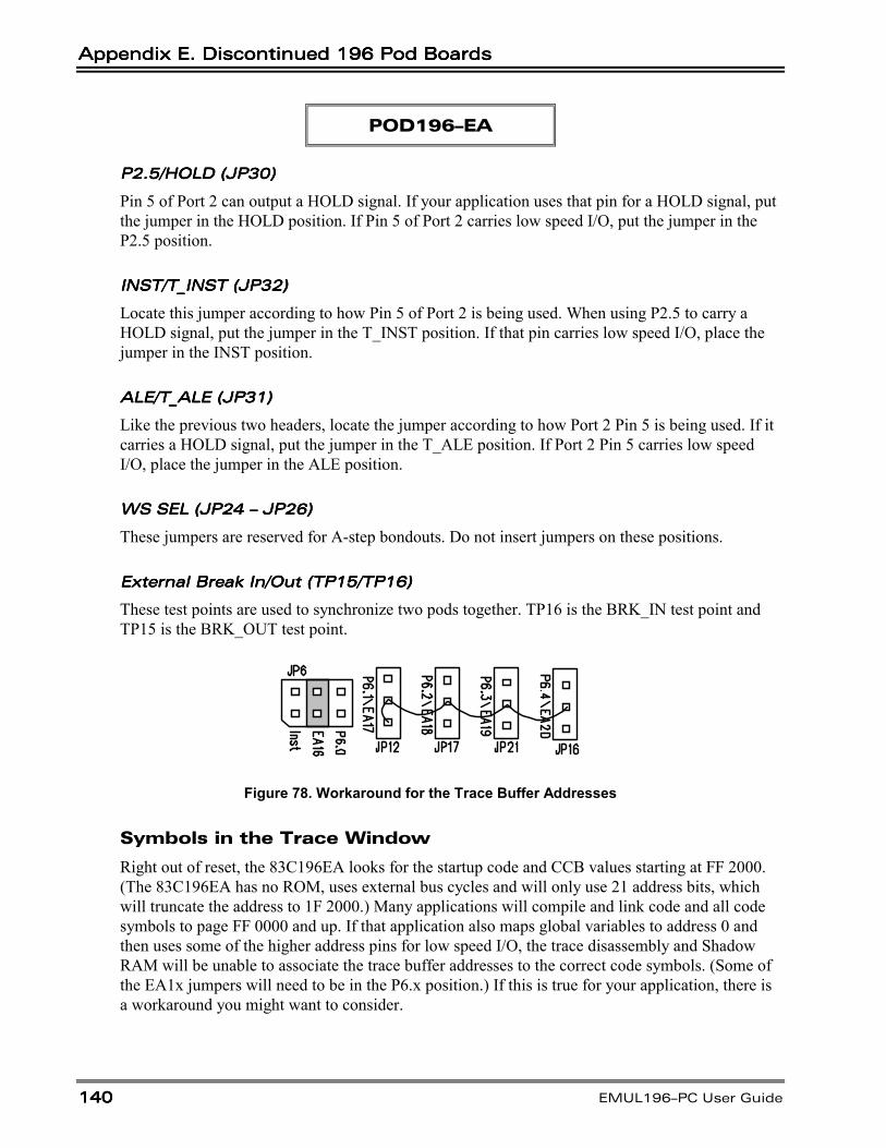
Appendix E. Discontinued 196 Pod BoardsAppendix E. Discontinued 196 Pod BoardsAppendix E. Discontinued 196 Pod BoardsAppendix E. Discontinued 196 Pod Boards
140140140140 EMUL196–PC User Guide
POD196–EA
P2.5/HOLD (JP30)P2.5/HOLD (JP30)P2.5/HOLD (JP30)P2.5/HOLD (JP30)
Pin 5 of Port 2 can output a HOLD signal. If your application uses that pin for a HOLD signal, putthe jumper in the HOLD position. If Pin 5 of Port 2 carries low speed I/O, put the jumper in theP2.5 position.
INST/T_INST (JP32)INST/T_INST (JP32)INST/T_INST (JP32)INST/T_INST (JP32)
Locate this jumper according to how Pin 5 of Port 2 is being used. When using P2.5 to carry aHOLD signal, put the jumper in the T_INST position. If that pin carries low speed I/O, place thejumper in the INST position.
ALE/T_ALE (JP31)ALE/T_ALE (JP31)ALE/T_ALE (JP31)ALE/T_ALE (JP31)
Like the previous two headers, locate the jumper according to how Port 2 Pin 5 is being used. If itcarries a HOLD signal, put the jumper in the T_ALE position. If Port 2 Pin 5 carries low speedI/O, place the jumper in the ALE position.
WS SEL (JP24 – JP26)WS SEL (JP24 – JP26)WS SEL (JP24 – JP26)WS SEL (JP24 – JP26)
These jumpers are reserved for A-step bondouts. Do not insert jumpers on these positions.
External Break In/Out (TP15/TP16)External Break In/Out (TP15/TP16)External Break In/Out (TP15/TP16)External Break In/Out (TP15/TP16)
These test points are used to synchronize two pods together. TP16 is the BRK_IN test point andTP15 is the BRK_OUT test point.
Figure 78. Workaround for the Trace Buffer Addresses
Symbols in the Trace Window
Right out of reset, the 83C196EA looks for the startup code and CCB values starting at FF 2000.(The 83C196EA has no ROM, uses external bus cycles and will only use 21 address bits, whichwill truncate the address to 1F 2000.) Many applications will compile and link code and all codesymbols to page FF 0000 and up. If that application also maps global variables to address 0 andthen uses some of the higher address pins for low speed I/O, the trace disassembly and ShadowRAM will be unable to associate the trace buffer addresses to the correct code symbols. (Some ofthe EA1x jumpers will need to be in the P6.x position.) If this is true for your application, there isa workaround you might want to consider.
EMUL196–PC User GuideEMUL196–PC User GuideEMUL196–PC User GuideEMUL196–PC User Guide
Edition 1, June 6, 2001 © 141141141
POD196–EA
Under these circumstances, to correctly associate addresses with symbols, the trace board needs toreceive an address that is different from the one appearing on the address pins. If you run a wirefrom the EA1x side of the highest TRA1x header not carrying an I/O signal to the center pins ofthe higher address headers, the trace board will get correct addresses for data space bus cycles.The following example will make it clearer.
The application in Figure 78 uses the three highest address pins for low speed I/O. The 256K x 8RAM chips need 18 address bits for holding data. These bits are bit 0 through bit 17. Again, theinstructions are mapped to the top of the address range: from FF 0000 to FF FFFF hex. Thiswiring ensures that when address Pin 17 is high, the trace boar will receive high signals forTRA17, TRA18 and TRA19. If this example application has global data symbols between20000 hex to 40000 hex, they will not be identified correctly in the Trace window. This wiringwill have no effect on how the trace displays global symbols below 20000 hex or local variablesfound on the stack.
Memory Mapping
While debugging your hardware and software, you typically want to use the RAM on your targetfor data and replace your EPROM with emulation RAM so you can reload and run your applica-tion quickly. Under most circumstances, this can be easily achieved with software memory map-ping. However, on pods with 256K of emulation RAM, only pages 1C to 1F are controlled bysoftware memory mapping. All other pages go to target.
If your requirement is for 256K of memory, but want it mapped at different pages, you use thehardware memory mapping. Remove JP40 (Auto-Map) and install JP44 though JP46 for the ap-propriate chip selects. You are required to program the chip selects and have jumpers installed forthe pod to access its memory.
NotePods sold with 2 MB of emulation RAM have the extra hardware to correctly mapevery address in software. On 1-MB pods, software memory mapping works onlyfor pages 10 – 1F. On a 2-MB pod, memory mapping works for the entire 0 – 1Faddress space.
Port Replacement Unit (PRU)
A PRU is a hardware device that uses logic to allow the pod controller to have the bus control sig-nals it needs while also allowing the applications to behave as though it has exclusive use of theshared pins. It fits between the pod and the Nohau adapters and is required to provide port signals.A 32-MHz PRU for POD196–EA, to provide Ports 3, 4, 5, and 12 as low-speed I/O.
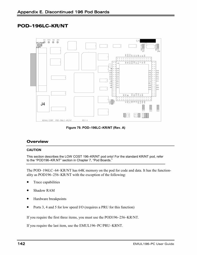
Appendix E. Discontinued 196 Pod BoardsAppendix E. Discontinued 196 Pod BoardsAppendix E. Discontinued 196 Pod BoardsAppendix E. Discontinued 196 Pod Boards
142142142142 EMUL196–PC User Guide
POD–196LC–KR/NT
J4
PC-PWR
XJP1
Figure 79. POD–196LC–KR/NT (Rev. A)
Overview
CAUTION
This section describes the LOW COST 196–KR/NT pod only! For the standard KR/NT pod, referto the “POD196–KR.NT” section in Chapter 7, “Pod Boards.”
The POD–196LC–64–KR/NT has 64K memory on the pod for code and data. It has the function-ality as POD196–256–KR/NT with the exception of the following:
• Trace capabilities
• Shadow RAM
• Hardware breakpoints
• Ports 3, 4 and 5 for low speed I/O (requires a PRU for this function)
If you require the first three items, you must use the POD196–256–KR/NT.
If you require the last item, use the EMUL196–PC/PRU–KRNT.
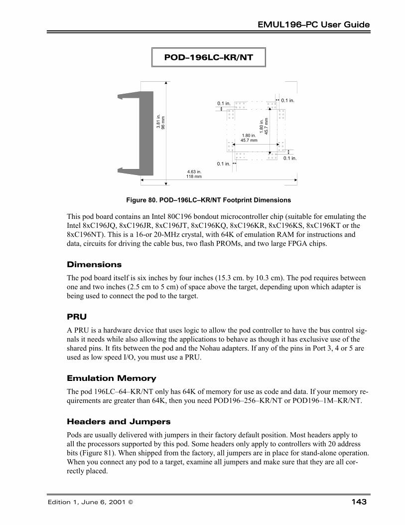
EMUL196–PC User GuideEMUL196–PC User GuideEMUL196–PC User GuideEMUL196–PC User Guide
Edition 1, June 6, 2001 © 143143143
POD–196LC–KR/NT
0.1 in. 0.1 in.
0.1 in.0.1 in.
1.8
0 in
.45
.7 m
m
1.80 in.45.7 mm
3.8
1 in
.96
mm
4.63 in.118 mm
Figure 80. POD–196LC–KR/NT Footprint Dimensions
This pod board contains an Intel 80C196 bondout microcontroller chip (suitable for emulating theIntel 8xC196JQ, 8xC196JR, 8xC196JT, 8xC196KQ, 8xC196KR, 8xC196KS, 8xC196KT or the8xC196NT). This is a 16-or 20-MHz crystal, with 64K of emulation RAM for instructions anddata, circuits for driving the cable bus, two flash PROMs, and two large FPGA chips.
Dimensions
The pod board itself is six inches by four inches (15.3 cm. by 10.3 cm). The pod requires betweenone and two inches (2.5 cm to 5 cm) of space above the target, depending upon which adapter isbeing used to connect the pod to the target.
PRU
A PRU is a hardware device that uses logic to allow the pod controller to have the bus control sig-nals it needs while also allowing the applications to behave as though it has exclusive use of theshared pins. It fits between the pod and the Nohau adapters. If any of the pins in Port 3, 4 or 5 areused as low speed I/O, you must use a PRU.
Emulation Memory
The pod 196LC–64–KR/NT only has 64K of memory for use as code and data. If your memory re-quirements are greater than 64K, then you need POD196–256–KR/NT or POD196–1M–KR/NT.
Headers and Jumpers
Pods are usually delivered with jumpers in their factory default position. Most headers apply toall the processors supported by this pod. Some headers only apply to controllers with 20 addressbits (Figure 81). When shipped from the factory, all jumpers are in place for stand-alone operation.When you connect any pod to a target, examine all jumpers and make sure that they are all cor-rectly placed.
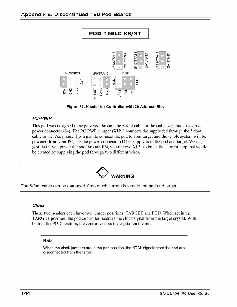
Appendix E. Discontinued 196 Pod BoardsAppendix E. Discontinued 196 Pod BoardsAppendix E. Discontinued 196 Pod BoardsAppendix E. Discontinued 196 Pod Boards
144144144144 EMUL196–PC User Guide
POD–196LC–KR/NT
BUSWIDTH JP6/TRA16 RST
BW
GN
D
VCC
M_I
NST
EA16
GN
D
JP13
JP14
JP15
JP12
\TR
A17
JP17
\TR
A18
EA17
\GN
D
EA18
\GN
D
JP21
\TR
A19
EA19
\GN
D
RXD HLD
JP5
Figure 81. Header for Controller with 20 Address Bits
PC-PWRPC-PWRPC-PWRPC-PWR
This pod was designed to be powered through the 5-foot cable or through a separate disk-drivepower connector (J4). The PC-PWR jumper (XJP1) connects the supply fed through the 5-footcable to the Vcc plane. If you plan to connect the pod to your target and the whole system will bepowered from your PC, use the power connector (J4) to supply both the pod and target. We sug-gest that if you power the pod through JP4, you remove XJP1 to break the current loop that wouldbe created by supplying the pod through two different wires.
WARNING
The 5-foot cable can be damaged if too much current is sent to the pod and target.
ClockClockClockClock
These two headers each have two jumper positions: TARGET and POD. When set in theTARGET position, the pod controller receives the clock signal from the target crystal. Withboth in the POD position, the controller uses the crystal on the pod.
NoteWhen the clock jumpers are in the pod position, the XTAL signals from the pod aredisconnected from the target.
EMUL196–PC User GuideEMUL196–PC User GuideEMUL196–PC User GuideEMUL196–PC User Guide
Edition 1, June 6, 2001 © 145145145
POD–196LC–KR/NT
In ONCE mode, (only while using a clip-over adapter), all the target controller pins are tri-statedexcept the oscillator pins. Because there is no way to disconnect the target crystal from the targetcontroller, the target crystal remains an active part of the clock circuit even when the jumpers aremoved to the POD position. Where the two oscillators are running at the same frequency, theysynchronize naturally. The presence of two oscillators does not affect how the application runs. Ifthey are different frequencies, you probably want to put both jumpers in the TARGET position anduse just the target oscillator.
PWRPWRPWRPWR
Remove this jumper when the target has its own power supply. When this jumper is in place, thetarget can get Vcc from the pod as long as the current requirement is less than 0.5 amps. Highercurrents cause a significant voltage drop along the current path and the pod can be damaged.
WARNING
For higher current requirements, use the power connector (J4) to supply both the pod and thetarget. Make sure to remove the PC-PWR jumper (XJP1).
RXD/TXD/GNDRXD/TXD/GNDRXD/TXD/GNDRXD/TXD/GND
This jumper is not functional. Do not insert a jumper on this header.
RSTRSTRSTRST
Occasionally, a target might contain an external device designed to reset the controller by pullingthe /RST pin low (i.e., a watchdog timer). The signal from the target /RST pin passes throughthe RST header. Removing the RST jumper prevents the external device from resetting the podcontroller.
HLDHLDHLDHLD
The target /HLD signal passes through the HLD header. Removing this jumper will prevent thepod controller from receiving the hold request from a target device.
BUSWIDTHBUSWIDTHBUSWIDTHBUSWIDTH
This header controls the signal sent to the FLEX logic chips. The bondout chip does not correctlyassert the bus control signals when the CCBs are set to have an 8-bit wide bus. If you need toemulate an 8-bit bus, you can do so reliably by setting the CCBs to have a dynamic bus width andadding a jumper to this header in the GND position. Have two jumpers on this header, one in theBW position and one in the GND position.
Appendix E. Discontinued 196 Pod BoardsAppendix E. Discontinued 196 Pod BoardsAppendix E. Discontinued 196 Pod BoardsAppendix E. Discontinued 196 Pod Boards
146146146146 EMUL196–PC User Guide
POD–196LC–KR/NT
If you have a PRU, refer to the Port Replacement Unit section for more information about the buswidth, the instruction width, and the CCB settings.
EA16-EA19EA16-EA19EA16-EA19EA16-EA19
The jumpers on these headers must remain in their default or grounded positions for all controllersthat use 16 address bits.
If your application uses a controller with 20 address bits, for every address above 15 that theapplication uses for addressing, move the corresponding jumper from the GND position to theEA1x position. This will pass that address signal to the on-pod memory. For each of the bitsthat are used for I/O instead of addressing, put the jumper on the GND side. This also appliesto JP\TRA16, even though it has a different geometry than the other headers.
WARNING
Do not put more than one jumper on EA16, also labeled JP6. Having two jumpers on this headercan damage the bondout controller or some other part of the pod.
INSTINSTINSTINST
The POD–196LC–KR/NT does not support this feature as it applies to customers whorequire more than 64K-address space. If this is the case, use the POD196–256–KR/NTor POD196–1M–KR/NT.
EMUL196–PC User GuideEMUL196–PC User GuideEMUL196–PC User GuideEMUL196–PC User Guide
Edition 1, June 6, 2001 © 147147147
GlossaryA
ABS file Many compiler assembler linker systemsput information about the source code, such assymbol definitions and line numbers in the ABSfile. Absolute load file generated by a linker op-eration after compiling/assembling the applicationcode. A superset of the 8051 OMF. A file con-taining absolute (i.e. fixed location) data to loadinto a computer.
Adapter The device that serves as an interface be-tween the system unit and the devices attached toit. A device used for making an electrical connec-tion between different package types, such asDIP40 to PLCC44. A connector or cable adapter,which changes one type of connector to another.
Address Refers to where a particular piece of data orother information is found. Also can refer to thelocation of a set of instructions. Normally, but notalways the words are 8-bit quantities. Some sys-tems might have a program memory with 12-bitwords and a data memory with 8-bit words.
Address Header The range of memory locationsthat are addressable by changing jumpers on theemulator and trace boards.
Address Space In Nohau emulators, there are oftenseveral address spaces. Each address space has adefined way of reading and usually writing to amemory. Several address spaces can address thesame physical memory in different ways that areconvenient for different usage. Some addressspaces can address spaces that cannot be accessedby any other address space. Some address spaces,such as Shadow might exist only in the NohauEmulator and not in the target system.
ASCII An acronym for American Standard Code forInformation Interchange. A coding scheme using 7or 8 bits that assigns numeric values up to 256characters.
Assembler An assembler is a program that convertsa symbolic representation of computer instructionsinto the representation that the computer requiresfor operation. In Nohau emulators, the assemblerwindow displays the contents of program memoryas a numeric quantity, and in a symbolic form thatis acceptable to an assembler for the processorbeing emulated. Information is lost in translation
when an assembler processes a program. Thesymbolic form that the Nohau emulator disassem-bles might not be exactly the original assemblerinput that produced the numeric quantity found inmemory.
B
Bank Number Translation In bank switching de-sign, cross-reference tables between bank numberand control byte pattern. This is necessary if thebit sequence of bank switching control signals isscrambled and not in order with the bit sequenceof control byte. This is not recommended.
Bank Switching A method of expanding the CodeMemory Space beyond that of microcontroller ad-dress bus limitation by creating additional high or-der address buses from a microcontroller 1/0 portor a memory mapped latch. The details varywidely. In general, one or more registers selectone of relatively large continuous banks of mem-ory to be accessed by a range of addresses. Seealso Memory window, page, paging, page register,and window.
Banking See also Bank Switching, Memory window,page, paging, page register, and window.
Base Register In the Motorola HCl2, HCl6, and683xx families a Special Register that sets thatstarting location of the block of Special Registersthat control the processor and the on-chip input /output devices.
Basic CPU Register The registers that Seehau ini-tially shows in the Register window. Some of theseregisters, such as the PC and SP can not be acces-sible in any other way. Others can be SpecialRegisters with a memory address that can beviewed and modified in several different ways inSeehau.
BDM An acronym for Background Debug Mode.This is a debugging mode available on some fami-lies of processors supported by Nohau emulators.The production processors dedicate a small num-ber of pins to the BDM functions. This allows asmall cable to connect an emulator and a produc-tion system that includes the processor. The emu-lator can then control the processor for debugging
GlossaryGlossaryGlossaryGlossary
148148148148 EMUL196–PC User Guide
in the production system. BDM emulator featuresare usually limited by the small size of the cable.
BERG connector A 10-pin connector used to con-nect a BDM pod to a target system.
Big Endian Having the bytes of a multi-byte numberordered with the most significant (biggest) bytefirst. Motorola usually uses this order. See alsoEndian, and Little Endian.
Binary Data Refers to the computer numbering sys-tem that consists of two numerals 0 and 1 Alsocalled base-2.
BNC connector An acronym for Bayonet Neil-Councelman, British Naval Connector, Baby N-connector, or Bayonet-Nut-Coupler. A connectorfor coaxial cables that locks when one connector isinserted onto another and rotated 90 degrees.Trace boards have two additional input / outputconnectors on the back called BNC connectors forTRIGGER-IN and TRIGGER-OUT recording.
Bondout Short for bondout chip. A special variationof a processor that brings out (bonds out to addi-tional pins) many extra internal signals. These ad-ditional internal signals allow the emulator todisplay and control internal states and functionsthat cannot be accessed in the mass productionversion of the processor.
Bondout Chip See also Bondout, Bondout Emula-tion, and Bondout Pod.
Bondout Emulation The emulation processor onthe pod is a special bondout processor, which usu-ally features more pins than a standard productionprocessor. Also they are more expensive due tolow production volume. See also Bondout,Bondout Chip, and Bondout Pod.
Bondout Pod A pod that has a bondout emulationprocessor. See also Bondout, Bondout Chip, andBondout Emulation.
Boot To load a program into the computer. The termcomes from the phrase pulling a boot on by thebootstrap.
Bootstrap A technique or device designed to bringitself into a desired state by means of its own ac-tion. The term is used to describe the process bywhich a device such as a PC goes from its initialpower-on condition to a running condition withouthuman intervention. See also Boot.
Break To stop the execution of a processor in a waythat allows the processor to resume execution as ifnothing had happened.
Breakpoint A debugging feature that breaks theprocessor at a particular location in a program orwhen a particular data item is accessed. This canbe a software breakpoint or a hardware breakpoint.See also Breakpoint Replacement.
Breakpoint Replacement If enabled, the emulatorwill stop right before the breakpoint, otherwise itwill stop right after the breakpoint. This appliesonly to hardware breakpoints. See also Break-point.
BSW See Bank Switching.
Buffer A block of memory used as a holding tank tostore data temporarily. A region of memory tohold data that is waiting to be transferred betweentwo locations as between an application's data andan 1/0 device.
Byte A collection of bits that makes up a character orother designation. Generally, a byte is 8 data bits.When referring to system RAM, an additionalparity bit is also stored, making the total 9 bits.
Byte Order The order of bytes in a word. Someprocessors (for example Motorola) store the mostsignificant byte first and others (for example Intel)store the least significant byte first. It appears thatthere is no decisive advantage to either scheme. Inmachines without hardware support for words (forexample the 8051) some compilers use one orderand some use the other. One compiler even usesone order for integers and the other for floatingpoint. See Big Endian and Little Endian.
C
CCR Acronym for (Emulator) Configuration ControlRegister. These registers are used to control theconfiguration of the emulator as contrasted withthe registers in the system being emulated.
EMUL196–PC User GuideEMUL196–PC User GuideEMUL196–PC User GuideEMUL196–PC User Guide
Edition 1, June 6, 2001 © 149149149
Chip An integrated circuit. Used to refer to processoror memory integrated circuits
Chip Select A type of signal generated by someprocessors that is suitable for connecting to a chipselect (CS) input of a memory chip. This allowsthe connection between the processor and thememory to be about as simple as connecting theaddress lines, the data lines, and the chip select.
Code coverage A feature of some Nohau emulatorsthat records the fetching (in the 196, 16, and 300)or the execution of instructions. Useful for evalu-ating the effectiveness of a test suite. If the test hasexecuted an instruction once, this gives assurancethat the instruction can be executed without faultin at least one case. If an instruction has not beenexecuted at all, there is a danger that it cannot beexecuted without causing an error.
COFF An acronym for Common Object File Format,a format for load files derived from the UNIXculture.
Command Line The line on the display screenwhere a command is expected. Generally, thecommand line is the line that contains the most re-cently displayed command prompt.
Command Set A named set of commands. A set ofcommands used to perform specific operations /tasks with the emulator. A list of instructions rec-ognized by a microcontroller.
Compiler A program that converts a symbolic de-scription of a computer program into a form thecomputer can execute. Compilers are distinguishedfrom assemblers in that they accept input that isnot directly related to the actual machine instruc-tions. The output from a compiler is called an ob-ject program. Most Nohau emulators support Cand C++ compilers by reading extra informationprovided by the compiler. This allows the emula-tors to display the compiler source code that cor-responds to a program location and to display thevalues of variables in a style appropriate to theway they were defined in the source program.
Core Command A core command is a hardwarespecific operation command issued by the userinterface. Core commands are processed by thecore part of Seehau to deal with the target hard-ware, file loading, and keeping the symbol table;unlike a GUI (Graphical User Interface) commandthat only affects the appearance of a window.
CPU symbol Default symbolic reference to the mi-crocontrollers Standard CPU registers. Symbolsused in the microcontroller CPU architecture defi-nition, especially for Special Function Registers(SFR), usually related with a SFR physical ad-dress.
CPU An acronym for Central Processing Unit. Thecomputational and control unit of a computer; thebrains. This device interprets and executes in-structions.
Crystal A frequency determining element. A reso-nating crystal used in a clock circuit for the micro-controller. A piece of silicon that oscillates at apredetermined frequency. An oscillator of somekind drives all microcontrollers. The device on thepod or the target that provides time base for theclock generation circuitry in microcontroller. Usu-ally required to be connected to two crystal pinson the microcontroller. It determines the operationspeed for the microcontroller. There is usually afrequency multiplier or divider involved, i.e. 5-MHz crystal *4 (multiplier) = 20-MHz SystemClock. See also Internal Crystal and ExternalCrystal.
Cycle Type A named sequence of events. A categoryof instruction action in a machine cycle usuallyrelated with a chip-select or strobe signal issuedby the microcontroller. For example, in the 8051family, there are Opcode Fetch Cycles (/PSEN),XData Write Cycles (IWR), and XData Read Cy-cles (/RD). Cycle type refers to the default symboltable that has been defined by Nohau for the mi-crocontrollers internal registers.
D
D connector See DB-25 connector.
Data Bus Width Override Determines how muchdata can be transmitted at one time. For example, a16-bit bus can transmit 16 bits of data, whereas a32-bit bus can transmit 32 bits of data.
Data Window A window in Seehau user interfacethat displays data stored in memory.
68HC12 MCU chip feature that allows a section ofthe 16-bit address space to address pages of dataspace. The DPAGE register controls the pagevisible in the window.
GlossaryGlossaryGlossaryGlossary
150150150150 EMUL196–PC User Guide
DB-25 connector A 25-pin D-shell connector pri-marily used for PC parallel ports. The mechanicalinterface of a 25-wire cable with a male (M) andfemale (F) DB-25 pin connector attached to eitherend. A plug with 25 pins or receptacles, each ofwhich is attached to a single wire with a specificfunction. Originally called an RS-232 (now EIA-232), the latest which defines not only the type ofconnectors to be used but also the specific cableand plugs and the functionally of each pin. In No-hau culture also referred to as a D connector.
Debug File A file generated by C Compilers / As-semblers, which contains both code and symbolcross-reference in the source file. The file usuallyhas a special filename extension such as OMF,ABS, or no extension at all. To get symbol infor-mation, the debug file should be loaded into theSeehau software. Hex files will not provide sym-bol information.
Delay The number of trace frames collected after atrigger event occurs.
Dialog box A special window displayed by the sys-tem or application to solicit a response from theuser.
Double A C floating point type usually representedin 64 bits.
DPRAM An acronym for Dual-ported RAM.DPRAM is a dual-ported random access memorywith separated ports of different bus width forREAD and WRITE function. The bus width is 1bit for READ and 16 bits for WRITE. The READand WRITE access can be performed simultane-ously or at independent clock rates at frequenciesup to 50 MHz.
DRAM An acronym for Dynamic Random AccessMemory. A form of semiconductor random accessmemory. Temporary storage that must be re-freshed over time.
DWARF An acronym for Debug With Arbitrary Rec-ord Format. The debugging information format as-sociated with the ELF load file format. Designedfor the better support of C++. See also ELF.
E
Edge connector The part of a circuit board con-taining a series of printed contact that is insertedinto an expansion slot or connector. The part ofthe expansion board that is inserted into the moth-erboard. See also Expansion Board.
EEPROM An acronym for Electrically Erasable Pro-grammable Read Only Memory. A type of non-volatile memory chip used to store semipermanentinformation. An EEPROM can be erased and re-programmed directly in the host system withoutspecial equipment. Read Only Memory (ROM)that can be electrically erased and programmedtoo repeatedly. Also called flash ROM. See alsoFlash Memory.
ELF An acronym for Executable and Linkable For-mat. A file format for program and data to beloaded into a processor. Usually associated withthe DWARF debugging information format. Seealso DWARF.
Emulator A piece of test apparatus that emulates orimitates the function of a particular chip. This de-vice runs the code in the same way and at the samespeed as the real microcontroller. The emulator fa-cilitates debugging by providing more informationabout internal operations of the microcontroller.The emulator gives better control of operationsand faster more flexible loading of programs.
Emulator Board An ISA card, which is pluggedinto PC or an HSP box with emulation memoryonboard. It is connected to a pod through a specialflat cable. In some emulators the functionality ofthe emulator board is integrated into the pod so, itmight not be available separately.
Emulator Memory Memory internal to the emula-tor. Some emulator memory can be used for theinternal purposes of the emulator that will notnormally be visible to the emulator user. Memoryprovided in the emulator that makes code debug-ging possible without a target. Overlay memoryfor the emulator to simulate the memory for On orOff chip memory.
EMUL196–PC User GuideEMUL196–PC User GuideEMUL196–PC User GuideEMUL196–PC User Guide
Edition 1, June 6, 2001 © 151151151
Emulation Mode The emulation processor on thepod running customer application code to enable itto simulate a real target processor.
Emulation Processor The processor provided onthe pod, which is used to emulate a target proces-sor. It might or might not be the same as the targetprocessor.
Endian The bytes, which are most significant in amulti-byte word. See Little Endian and Big En-dian.
Environment settings User interface setups for thedebug environment such as load path, source filepath(s), file load options, etc.
EPAGE A register in some Motorola 68HC12 familymembers that controls what page of Extra memoryit mapped into the Extra Page window. See theMotorola User’s Guide for the particular familymember for further information
EPC An acronym for Emulator Parallel Cable. A No-hau product that attaches an emulator to a laptopcomputer parallel (printer) port.
EPROM An acronym for Erasable ProgrammableRead Only Memory. A type of ROM that can beerased by exposure to ultraviolet light and pro-gramming repeatedly. See also EEPROM.
Expanded Mode See External Mode.
Expansion Board Any board that plugs into one ofthe computer's expansion slot. Expansion boardsinclude controller boards, trace boards, and emu-lator boards.
Expansion Card See Expansion Board.
External Crystal The crystal on the target is usedfor the crystal source of emulation processor.
External Mode The code and or data memory isexternal to the microcontroller. Some ports on themicrocontroller are functioning as data bus and/oraddress bus. See also Single Chip Mode.
External Mode Pod A pod whose emulation proc-essor works in External Mode. The same as astandard production processor.
External Power The emulation processor on thepod gets power from the target. Recommended forBondout pods and Low Voltage Emulation. Theexternal power can be used only when the target isconnected to the pod.
Extra Window A 68HC12 MCU chip feature thatallows a small section of the 16-bit address spaceto address pages of extra space. The EPAGE reg-ister controls the page visible in the window.
F
Fast Break Write A feature of some Nohau emula-tors that allows writing to target memory while thetarget is running. It causes minimal interruption tothe target execution. It does stop (break) the targetprocessor for a short time.
Filter A set of conditions that determine whichframes are allowed into the trace buffer. Filteringselects the type of information in an address range,and the type of data that is recorded in the tracememory. This is a distinct action separate fromFilter Mode.
Filter Mode This mode is different from filter. SeeWindow Filter and Normal Filter.
Flash ROM Flash ROM, also known as flash. A typeof EEPROM that has been optimized for faster(flash) erasing and programming. See alsoEPROM and EEPROM.
float A C type for floating point numbers. Often 32bits in length.
Floating Point The computer version of ScientificNotation for numbers. A fraction and an exponentrepresent the number.
Frame A unit of information in a trace buffer. Usu-ally a record of a target memory reference, but canrecord other events such as a low power state orthe passage of time.
Frame Number An arbitrary number assigned bythe emulator to each frame in a trace buffer. Posi-tive frame numbers occurred after the trigger andnegative frame numbers occurred before the trig-ger. If a trigger did not stop tracing, the last re-corded frame number is -1.
GlossaryGlossaryGlossaryGlossary
152152152152 EMUL196–PC User Guide
Frequency Multiplication Multiplying externalclock input signal's frequency by a factor and feedit to the CPU inside a microcontroller. Often doneby a Phase Lock Loop (PLL) circuit inside the mi-crocontroller. Electromagnetic Interference (EMI)is reduced this way. A factor used by a microcon-troller to multiply the crystal (oscillator) fre-quency, i.e. 5-MHz crystal *4(multiplier) = 20-MHz System Clock.
Frequency limit The maximum or minimum fre-quency at which an emulator is designed to oper-ate properly.
Full Emulator An emulator with the ability to addtrace capabilities. Full emulators often use theBDM pins on the processor to do some of theemulator functions in addition to providing trac-ing, shadow memory, and more breakpoints.
G
GPT An acronym for the General Purpose Timer, ahardware feature found on some Motorola embed-ded processors.
GUI Command GUI commands are graphical userinterface commands that allow you to choosecommands and functions by pointing to a graphi-cal icon using either a keyboard or pointing devicesuch as a mouse, trackball or touch pad. Seehauhas a GUI part that handles the display and controlfor the user. This part is common to all Nohauemulator families. The Seehau GUI sends com-mands to the core (see Core Command) which isspecific to a particular family of processors. Thesecommands can be recorded in macros. To allowmacros to affect the display, the GUI also sendscommands to itself.
H
Hardware Breakpoint A breakpoint function im-plemented in hardware, either in a processor chipor in an emulator. The distinguishing feature is thehardware, which does not require any softwaremodification to place the breakpoint. This allowsbreakpoints to be effective in ROM of all kinds.See also Breakpoint, and Software Breakpoint.
Hex Hexadecimal, a number encoded as base-16 in-stead of base-10. Widely used for display of mem-ory addresses and hardware registers becausehumans and computers more easily translate it intobits than standard decimal notation. See alsoHexadecimal.
Hex File An ASCII file consisting of a number ofHex records, which represent machine languagecode and / or constant data with hexadecimalnumbers. A load file or absolute file with the datain hexadecimal numbering (base-16). It is usuallyused to transfer the program and data that wouldbe stored in a ROM or EPROM. No symbol / de-bug information is included in the Hex file. Nohausupports a standard hex file format for each fam-ily, Motorola S-Record or S19 for Motorola fami-lies, and Intel Hex for Intel families. Othermanufacturers adopt one or the other as their hexfile format standard.
Hexadecimal A numbering system used in comput-ers. 16 characters: 0 through 9, and A through F(upper or lower case) to represent the numbers 0through 15. One hexadecimal digit is equal to 4bits, and one byte is two hexadecimal digits. Seealso Hex.
High Speed Parallel Box See HSP.
Hooks Emulation Mode The emulation processoron the pod is a standard production microcontrol-ler, but is put into a special Hook's mode, whichmakes the emulation possible.
Hooks Mode A special emulation mode that is builtinto specific microcontrollers. A special operationmode, in which the microcontroller provides extrainternal signals via unused bus cycles, emulatorcircuitry also controls the microcontroller throughthese cycles. It is an extra feature built into the mi-crocontroller. An emulation mode peculiar tosome 8051 derivatives.
Hooks Mode Pod A pod whose emulation proces-sor works in Hooks Emulation mode.
HSP A box with its own power supply, which canhold an emulator board and, or an optional traceboard. TheHSP box contains a motherboard with three ISAslots. The HSP box allows the use of the in-circuitemulator and optional trace board when no ISAslots are available in your PC. The HSP connectsto the PC printer port, so it can be used with alaptop computer or a standard PC. It is valued for
EMUL196–PC User GuideEMUL196–PC User GuideEMUL196–PC User GuideEMUL196–PC User Guide
Edition 1, June 6, 2001 © 153153153
power-up, and power-down emulator convenience.See also High Speed Parallel box.
HSP card An ISA board in the HSP that connects toa PC through a cable from the serial interface onthe card to the parallel port on the PC or laptopcomputer.
II/O Input/Output. A circuit path that enables inde-
pendent communications between the processorand external devices.
I/O Port Input/Output port. Used to communicate toand from devices, such as a printer or disk.
IC An acronym for Integrated Circuit. A completeelectronic circuit contained on a single chip. Seealso Chip.
IEEE–695 A widely supported load file format speci-fied by IEEE (Institute of Electrical and Electron-ics Engineers) standard 695.
Inspect Window A Seehau user interface windowthat displays current value of the selected item.The window is updated each time emulationbreaks. It can be used for evaluation and modifi-cation of some expressions as well as of C andC++ variables using the symbols of the currentlyloaded program.
int A C type for integer.
Integer A whole, or ordinal number. A number with-out a fractional part, for example 1.
Intel absolute object format Absolute file formatdefined by Intel. (INTEL OMF) A debug file for-mat defined by Intel Corporation in 1982. A su-perset of the 8051 OMF. See also ABS.
Intel Byte Order Having numbers represented by asequence of bytes with the first byte holding theleast significant 8 bits of the number. See also Lit-tle Endian.
Intel Hex A load file format. This format is a text filewith the addresses and the data to be loaded inhex. This format makes no provision for commu-nicating symbol values to the emulator software.
Internal Crystal The factory default crystal on thepod is used for the crystal source of emulationprocessor.
Internal Power The emulation processor on the podgets power from the emulator board. Recom-mended in all times except for bondout pods andlow voltage emulation.
Internal Symbol Table The default, built in sym-bols. See also Symbol Table.
Interrupt Vector Table A table, which keeps across-reference between interrupt source and thestarting address of the corresponding interruptservice subroutine. See also Vector Table.
ISA An acronym for Industry Standard Architecture.The original IBM PC-AT plug-in card format andbus structure. Some Nohau emulators plug intothis bus.
ISA slot A connection socket for a peripheral de-signed according to the ISA standard that appliesto the bus developed for use in the 80286 mother-board.
Isolator An adapter, which has many small switchesin the middle so the user can connect or discon-nect, signals selectively. Used in target connectiontroubleshooting.
JJargon File A dictionary widely available on the
Internet that defines many obscure informal com-puter terms, such as Big Endian and Little Endian.
Jumper A small, plastic-covered metal clip that slipsover two pins protruding from a circuit board.Sometimes also called a shunt. When in place, thejumper connects the pins electrically and closesthe circuit. By doing so, it connects the two termi-nals of a switch, turning it on. A group of jumpersare referred to as a jumper block.
LLC–ISA An acronym for Low Cost-Industry Standard
Architecture. This is aBackground Debugging Mode (BDM) pod. Seealso BDM.
GlossaryGlossaryGlossaryGlossary
154154154154 EMUL196–PC User Guide
LED An acronym for Light Emitting Diode. A semi-conductor diode that emits light when a current ispassed through it.
Linker A program that takes relocatable object filesproduced by compilers and assemblers and com-bines them with precompiled library programs intoa load file that can be loaded into a target proces-sor. The linker usually puts the symbols defined inthe source programs into the load file in a way theemulator loader can decode.
Little Endian Having the bytes of a multi-byte num-ber ordered with the least significant littlest bytefirst. Intel usually uses this order. See also BigEndian.
Load file A file that contains a program in binaryform to be loaded into the target. Nohau emulatorssupport many formats of load files. Most formatsinclude the final translated values of the symbolsused in the original source files.
Locator A term used for a linker that takes directivesfor setting the locations in the target processor ofthe various arts of the program.
long A C type for integer that is at least as big as int.Usually 32 bits or 64 bits.
Low Voltage Emulation The target works at avoltage lower than 5V DC, such as 3V DC. Exter-nal power is required. LPT PortLine Printer port,is a common system abbreviation for a parallelprinter port.
LSB First An acronym for Least Significant Bit first.Having numbers represented by sequence of byteswith the first byte holding the least significant 8bits of the number. See also Little Endian.
MMacro A set of keystrokes and instructions recorded
and saved under a short key or macro name. Usedto save time by replacing an often-used, some-times lengthy, series of strokes with a shorter ver-sion.
Maximum frequency The frequency limit on thepod.
MCU An acronym for Micro Controller Unit. Industryjargon for a single-chip computer of some kind.
Memory The storage parts of a computer. Usuallyorganized into addresses, which pick one of manylocations that each hold, the same number of bits.Often the contents are bytes of 8 bits.
Memory Dump The hexadecimal representation ofan area of memory. The copying of raw data fromone place to another with little or no formatting forreadability. Usually, dump refers to copying datafrom main memory to a display screen or a printer.Dumps are useful for diagnosing bugs.
Memory Image A copy of one area of memory inanother area of memory. See also Shadow RAM.
Memory Mapping Controls the operation of selec-tion between emulation memory and the users tar-get memory. Any memory address can be eithermapped to emulator memory or target memory. Ifit is mapped to emulator memory, it will bemapped to RAM on the emulator itself and thememory space on the target will be ignored. If it ismapped to target, whatever device on the target(RAM, ROM, I/O) will be used and the corre-sponding emulator memory (RAM) will be ig-nored.
(memory) Page A section of a memory with alarger address range that is accessed in a smallerwindow (Q.V.) in an address space with a smalleraddress range. The page (number) or page registersupplies the most significant bits of the larger ad-dress, and the address in the smaller window sup-plies the least significant bits of the address.
Individual families of processors, and individualmodels within families have unique variations inthe details of paged addressing schemes. If youhave to understand a particular scheme, read themanufacturer's documentation carefully. See alsobanking, bank switching, memory window, page,paging, page register, and window.
Memory Space Memort space is a range of memorythat is accessible to a microcontroller, and can beused for different purposes, but can occupy thesame addresses in memory. The number of addresslines used usually determines the size of thisspace. The property of physically or logicallyseparate memory blocks, which are accessed bydifferent type of instructions such as code, externaldata, and internal data.
Menu A list of options from which you can select inorder to perform a desired action.
EMUL196–PC User GuideEMUL196–PC User GuideEMUL196–PC User GuideEMUL196–PC User Guide
Edition 1, June 6, 2001 © 155155155
MHz An abbreviation for megahertz, a unit of meas-urement indicating the frequency of one millioncycles per second.
Micro-clip A series of wires connected to the DB-25connector on one end and small clips attached tothe wires on the other end. Rather than a ribboncable there are individual wires emanating fromthe connector that can be used for input and outputdata. The ends with the small clips can be attachedto the target system.
Mixed mode A display format for Seehau sourceand trace windows where the source lines are dis-played with the disassembled instructions thatwere compiled from the source line.
Monitor Mode The emulator actions are being ob-served in this mode. The emulation processor isrunning Emulator Monitor Code. Microcontrollerspecific code that runs when the emulator is notrunning the user application code. When there isno program execution going on, but we still haveto access memory, registers and set up windows,etc. Monitor mode runs everything except the tar-get program execution.
Motorola absolute object format Absolute fileformat defined by Motorola. (MOTOROLACOFF)
Motorola Byte Order Having numbers representedby a sequence of bytes with the first byte holdingthe most significant 8 bits of the number. See alsoBig Endian.
Motorola Families Groups of microcontrollers thatare closely related in characteristics that are manu-factured by Motorola.
MSB First An acronym for Most Significant Bit first.Having numbers represented by a sequence ofbytes with the first byte holding the most signifi-cant 8 bits of the number. See also Big Endian.
N
ncore.log Log file produced by the operation ofemulator, contains information of the data passedbetween the CORE level program and the usersinterface. The Log to file check box in the Envi-ronment Configuration, Options tab controls thewriting of this log file. The file is written to the di-rectory where Seehau.exe is installed.
New Hacker’s Dictionary A very useful dictionaryof computer jargon published by the MIT press.See also Jargon File.
Normal Filter Mode In this mode the last enabledtrigger can be assigned a repeat counter thatcauses the trace to look for this last trigger a num-ber of times before a trigger is recognized.
O
OLE automation An acronym for Object Linkingand Embedding. A distributed object system. Theability for an external program, that is or containsa programming language, to control another pro-gram.
OMF file A debug file format, abbreviation of ObjectModule Format. Object Meta File -industry basestandard. A load file format.
Oscillator A self-contained device which generates aclock signal of a specified frequency without theassistance of external feedback circuitry. Its outputusually can be fed directly to the clock-input pinof a microcontroller.
P
P & E A manufacturer of software. A symbol fileformat used with Motorola MCUs is named forthem.
Page A fixed-size block of memory whose physicaladdress can be changed through mapping hard-ware.
Paging A method of expanding a computer's mem-ory beyond the limits of an address size. A tech-nique for implementing virtual memory. Thevirtual address is divided into a number of fixed-sized blocks called pages, each of which can bemapped onto any of the physical addresses avail-able on the system. One or more registers selectone of relatively large continuous pages of mem-ory to be accessed by a range of addresses. Some-times used as a synonym for bank switching.
GlossaryGlossaryGlossaryGlossary
156156156156 EMUL196–PC User Guide
Paged Addressing See Bank Switching.
PC Common industry acronym for Program Counter,but also used to mean Personnel Computer. Seealso Program Counter.
Pipelined Architecture A computer architecturethat speeds up the instruction execution rate byexecuting each instruction in stages, and executingdifferent stages of several instructions at the sametime. A common set of stages is Instruction fetch,data fetch and data store. In a computer with thistype of pipelined architecture a single instructionwould progress through these stages in sequence.
At the same time the computer might be doing:fetch of instruction 3data fetch for instruction 2data store of the results of instruction 1
At the next cycle the computer would be doingfetch of instruction 4data fetch for instruction 3data store of the results of instruction 2
A confusing side effect of this architecture is thatthe memory references for instructions and data,can not be in the order one would expect fromwhat instructions the computer is executing. (No-tice that in the preceding example, instruction 3 isread from memory before the results of instruction2 are stored.)
The trace feature of Nohau emulators for proces-sors with pipelined architecture make an effort toclarify this confusing situation by giving either ahardware view showing the memory references inthe actual order on the memory bus, or a softwareview showing the memory references as they arelogically executed by the computer.
For historical reasons, the terms for the hardwareand software views are not uniform among the dif-ferent computer families supported by Nohau.
PLCC An acronym for Plastic Leaded-Chip Carrier.A popular chip-carrier package with J-Ieadsaround the perimeter of the package.
Plug-and-sleeve connector A connector type thathas nine or more different sizes that look almostthe same. It is necessary to get an exact size matchto get reliable operation.
Pod A small module of electronics or a circuit board,which contains an emulation processor and someaccessory circuitry that, connects the emulator tothe target via an adapter. This can be a small plas-tic container with a circuit board inside or an opencircuit board with exposed pins that connect to thetarget system. See also Bondout Pod, Hooks ModePod, and External Mode Pod.
Power Selection To determine whether to use in-ternal power or external power for the emulationprocessor on the pod. Usually controlled by ajumper on the pod.
Power supply (short and long tail) An electri-cal/electronic circuit that supplies all operatingvoltage and current to the system. There are twopower supply units for powering the emulators.Both of these units are 5-volt, 6-amp units, butwith one difference; one has a short tail (the lengthof the power cord from the converter to the plug)and the other a long tail. The long tail is used forpowering the BDM pods only, not the HSP box.The short tail power supply unit can be used forpowering the BDM pod or the HSP box.
PPA (Program Performance Analyzer) A statis-tical tool used to collect information from a cur-rently executing program. Displays the number ofclock cycle functions required for accessing data.
PPAGE A register in some Motorola 68HCl 2 familymembers that controls what page of programmemory it mapped into the Program Page Win-dow. See the Motorola User’s Guide for the par-ticular family member for further information.
Program counter A contraction of the more de-scriptive Program Location Counter. Often abbre-viated to PC. The program counter indicatorsprovide line number information supplied by com-piler manufacturers. The register in a computerthat holds the address of the current instruction.Normally it is incremented by the size of each in-struction as the instruction is fetched from memoryto be executed. (Jump, Branch and Call instruc-tions can change the PC to a new, out of sequencelocation.) Interrupts also change the PC.
Program Step General term for one of four emula-tor features that allow the user to see the results ofprogram execution in a step by step fashion. Theyare: Source Step Over, Source Step Into, Assem-bler Step Over and Assembler Step Into.
EMUL196–PC User GuideEMUL196–PC User GuideEMUL196–PC User GuideEMUL196–PC User Guide
Edition 1, June 6, 2001 © 157157157
Program Window A 68HC12 MCU chip featurethat allows a section of the 16-bit address space toaddress pages of program space, usually on chipflash memory. The PPAGE register controls thepage visible in the window.
PWM An acronym for Pulse Width Modulator orPulse Width Modulation. Embedded computersoften have a PWM output unit. This unit generateslogic outputs with variable widths and selectablerates. These pulses are frequently averaged to givea variable voltage between logic high and logiclow.
R
RAM An acronym for Random Access Memory. Allmemory accessible at any instant (randomly) by amicroprocessor. Used to refer to the read/writememory of an embedded computer system.
Register Storage area in memory having a specifiedstorage capacity, such as a bit, a byte, or a com-puter word, and intended for a special purpose.Something that holds a value. A set of high-speedmemory within a microprocessor or other elec-tronic device. A collection of electronic circuitsthat holds a number. Used in reference to memorylocations. In Seehau documentation, we refer tomany kinds of registers. Among them are SpecialFunction Registers (SFR), Configuration ControlRegister (Emulator (CCR)), Special Register, BaseRegister, Basic CPU Register and User-DefinedRegister.
Reset and Go A feature of Nohau emulators thatapplies a reset signal to the target system and thenstarts it immediately. This simulates the real-worldeffects of a short power failure. Useful for testinginitialize code, especially on systems that limit thewriting of some registers to a small fixed numberof cycles after a reset.
Ribbon cables A flat cable containing up to 100parallel wires for data and control lines. NohauCorporation uses these cables to connect the podboards to the PC or HSP and the trace board to theemulator board.
ROM An acronym for Read Only Memory. A type ofmemory that has values permanently or semiper-manently burned in. Often used in imbedded sys-tems for program storage. Older versions canrequire a special process at the semiconductor fa-
cility to program. See also EPROM, EEPROM,and Flash.
Rotational Cable A cable adapter that allows con-nection of a pod to a target with a thin cable thatcan go out over the target system in the directionof any side of the target processor. Very useful forconnecting an emulator to a cased target system
S
S19 A load file format. This format is a text file withthe addresses and the data to be loaded in hex.This format makes no provision for communicat-ing symbol values to the emulator software.
SAX A subset of Microsoft's Visual Basic. SAX is version of a micro code languagethat is somewhat compatible with VisualBasic.
Seehau A high-level language user interface thatallows you to perform many useful tasks includingthe following: Load, run, single-step and stop pro-grams based on C or Assembly code. Set tracetriggers and view trace. Modify and view memorycontents including Registers. Set breakpoints.Analyze code with Program Performance Analy-sis.
Set Breakpoints A directive to actually placehardware or software breakpoints into the targetsystem.
SFR An acronym for Special Function Register. Forsome microprocessor families, this has a precisemeaning spelled out in the microprocessor docu-mentation. For other families, it is used very im-precisely, but always to refer to registers in thesystem being emulated. See also Registers andSpecial Registers.
SFR branch Some Special Function Registers areBIT addressable, so the base register can bebranched to its BIT level definitions.
SFR symbol Default symbolic reference to the mi-crocontrollers Special Function Registers.
Shadow RAM A real time mapping of microcon-troller data memory. Updated in full speed emula-tion. Shadow RAM is used to duplicate thecontents of the target RAM. Every time the CPUgenerates a WRITE bus cycle, the pod captures
GlossaryGlossaryGlossaryGlossary
158158158158 EMUL196–PC User Guide
the address / data pair and the emulator boardwrites that data to the same address in ShadowRAM. The Nohau Shadow RAM feature allowsyou to view memory contents in real-time withoutstealing cycles from the emulation CPU.
short A C integer type that can be any size fromcharacter to integer.
Single-Chip Mode Code and/or data memory isinside the microcontroller. No address / data busavailable externally on microcontroller pins. Thismode can be emulated only by bondout pods orhooks mode pods. This mode cannot be emulatedwith external mode pods.
Software Breakpoint A breakpoint function im-plemented by replacing an instruction with anotherinstruction that causes the target system to stop inan orderly fashion (break). The distinguishingfeature is that no special purpose hardware is re-quired for placing the breakpoint. This allows alarge number of breakpoints. A software break-point can not function in ROM. See also Break-point and Hardware Breakpoint.
Solder Down A socket that is soldered down to aPCB in place of a microcontroller that allows anemulator adapter to be plugged in to the target cir-cuit. Some solder down sockets allow the micro-controller or the emulator adapter to be plugged.This usually consists of a detachable top half and asolder-down base, so that the pod can be easilyremoved. In contrast with a socketed connection.See also Solder Down Adapter and Solder DownBase.
Solder Down Adapter The adapter is soldereddown directly on the target surface mount foot-print, which replaces the socket. See also SolderDown and Solder Down Base.
Solder Down Base The lower half of a solderdown adapter assembly. Usually included in a sol-der down adapter assembly but can be orderedseparately.
Source A window in Seehau user interface that dis-plays the source program. See also Source Pro-gram.
Source Program An informal name for the programdescription that the software engineers or pro-grammers write for input to the compiler or as-sembler. The source of the intermediate files and
the final program that can be executed by thecomputer.
SP An acronym for Stack Pointer. See Stack Pointer.
Special Register In Motorola families, the memorylocations in the system being emulated that haveside-effects such as controlling input/output de-vices and processor configuration; as contrastedwith ordinary memory (RAM and ROM) locationsthat just hold data.
Seehau allows a user to add Registers - Add Reg-ister to define a new special register, Registers -Add Special Registers (SFR) to display a specialregister defined in a file and File - Load DefaultCPU Symbols to make the special register defini-tions available for disassembly and in-line assem-bly.
SRAM An acronym for Static Random Access Mem-ory. A type of RAM that will hold its contentswithout any electronic activity as long as power isapplied. See also DRAM (Dynamic Random Ac-cess Memory) which requires periodic electronicrefresh cycles to keep its contents.
Stack Overflow A situation where the Stack Pointerexceeds the maximum allowed value or falls shortof minimum possible value, and is pointing tosome address which, is not a stack. A conditionwhere the size of a stack has exceeded or at-tempted to exceed the memory allocated to thestack. Usually this happens when there is too manynested function calls. Not always recognizedautomatically, and generally prevents continuedcorrect operation of programs using the stack.
Stack Pointer A register that contains the currentlocation of the program stack.
Startup.bas A macro file that is used by Seehau toinput stored values for starting a previously setupproject.
Symbol A compiler symbol such as a variable orfunction name or an assembler symbol such as alabel or more generally, the information associatedwith a symbol. In Seehau, Loading Symbols refersto the process of reading the information that thecompiler and linker have provided about thesource of the program being loaded.
In addition to the detailed information about eachsymbol, this information includes the relation ofthe source file to the target processor instructions
EMUL196–PC User GuideEMUL196–PC User GuideEMUL196–PC User GuideEMUL196–PC User Guide
Edition 1, June 6, 2001 © 159159159
that are executed. If Seehau symbols are removed,information connecting the target memory with thesource code and symbols are also removed. There-fore, all source-related features such as the Sourcewindow and the Inspect/Watch window will ceaseto function.
Symbolic Data Included in many file load formatsto give the user the ability to debug their code withspecifics to symbol type, module, functions, etc.Symbolic data can be used to refer to files thatrepresent computer code with symbols, that is ei-ther assembler or compiler source files. It can alsorefer to compiler, assembler or linker output filesthat have preserved some of the original symbolicinformation for debugging.
Symbolic Format A format using identifiers ratherthan numbers. Accessing a component by its sym-bolic name.
System Clock The main CPU clock. The operatingfrequency of the microcontroller.
T
Target A general name for the embedded systembeing developed with the help of an emulator. Acustomer application circuit board, the microcon-troller on which is to be replaced by a pod duringemulation.
Time.bas A macro file used to run the timer programto test pods.
Timestamp A feature that displays the number ofmachine cycles that have elapsed since the begin-ning of program execution.
Trace A comprehensive tool used to analyze the mi-croprocessor environment. An emulator featurethat records detailed information about targetmemory accesses while the target system is in op-eration. Triggering features allow the trace to bestopped on conditions of interest so that the usercan look at the trace information and save it todisk without disturbing the operation of the target.
Trigger An event that stops trace buffer recording.
Tristated An output, which has a third state of highimpedance in addition to the regular high and lowstate. When tristated, there is a high impedanceseen by the rest of the circuit, there is no currentsourcing or sinking.
U
uP clock The uP Clock is the internal CPU clock ofthe microprocessor. This setting is used only forthe calculation of the trace time stamp.
User-Defined Register Registers added to the reg-ister window by a user using the Registers - AddSpecial Registers (SFR) menu item. They aresaved when the configuration settings are saved.Also used to refer to some of the symbols definedin a load file.
V
Vcc In electronic designs the supply for transistorcollectors originally, now usually the commonlyused positive power supply. The power supply inBipolar Integrated Circuits (IC) usually wired tothe transistor collector in the IC. Normally posi-tive 5 volts.
Vector Table A table of addresses to jump to whencertain actions occur. There is usually a start vec-tor where program execution starts, and an errorvector (hardware trap) where the controller jumpsto if a problem occurs, and many other vectors.
W
Window A portion of the screen that can contain itsown document or message.
A rectangular area of display on you monitor.
A section of target memory that is handled spe-cially. (For the HC12, see Program window, Datawindow and Extra window.)
Window Filter Mode Restricts the triggering logic,but allows recording only of references to program
GlossaryGlossaryGlossaryGlossary
160160160160 EMUL196–PC User Guide
or data areas of interest. More useful informationcan be collected in this mode before old informa-tion is overwritten in the trace memory.
Windows NT / 2000 / 95 / 98 Operating Systems(OS) produced by Microsoft Corporation. Win-dows 98 replaced Windows 95 and Windows 2000replaced Windows NT 4. These are the dominantOSs for PCs today.
X
XRAM Provides access to 2K of on-chip RAM.No external bus cycles are executed for theseaccesses.
EMUL196–PC User GuideEMUL196–PC User GuideEMUL196–PC User GuideEMUL196–PC User Guide
Edition 1, June 6, 2001 © 161161161
Index
3
3COM Etherlink III (905B or later) 10/100 PCI · 11
8
87C196CB Bondout Errata · 126Extended Addressing Bugs · 126PRU with /#EA Pin High · 126
8xC196 Port 5 Circuit · 80
A
Aborted Interrupt Vectors to Lowest Priority Bug · 131About This Guide · xAccessories and Adapters · 39Active Triggers · 33Adapters · 39
Clip-Over · 39Pin Grid Array · 39PLCC · 39Surface Mount QFP · 39Surface Mount SQFP · 39
address conflict · 96Address Cycle Type · 35Address Cycle Type/Data Trigger Mode · 37Address Cycle Type/Opcode Trigger Mode · 36address examples for emulator/trace
100 Hex Range · 117200 Hex Range · 118300 Hex Range · 119
Administrator Dialog Box · 17Alternative Addressing
for Windows 2000 · 20for Windows 95/98 · 12for Windows NT · 14
Assembler Notes · 115associating addresses with symbols · 71Autorun feature · 7
B
base address
for Windows 2000 · 20for Windows 95/98 · 12for Windows NT · 15
basic hardware · 125-pin to 50-pin cable · 1Emulator board · 1Five-foot ribbon cable · 1Pod board · 1Standard or Data trace board · 1Target adapter · 1
Bay Networks NetGear FA310TX 10/100 PCI · 11Bits Used for Addressing · 107black wire · 44BNC connectors · 29Break Emulation · 33BRK_IN · 42BRK_OUT · 42buswidth for CA/CB, troubleshooting · 108
C
CA device users · 126CB device users · 126CCB bits · 78CCB Settings · 79check list for troubleshooting · 95Checking Administrative Privileges
for Windows 2000 · 16for Windows NT · 13
Checking Your PC for Default Address Conflictsfor Windows 2000 · 18for Windows 95/98 · 12for Windows NT · 14
Chip Configuration Bytes (CCBs), troubleshooting · 107Chip Side of the KR/NT PRU · 74Clip-Over · 39clip-over adapter · 44Code coverage · 46Compiler Notes · 115
IndexIndexIndexIndex
162162162162 EMUL196–PC User Guide
CompilersIAR · 116–15Overview · 115Tasking · 115
Assembler Notes · 115Compiler Notes · 115
Configuring Address Settings for the Emulator and OptionalTrace Board · 11
Configuring Address Settings With Windows · 11Windows 2000 · 16Windows 95/98 · 12Windows NT · 13
Configuring Address Settings with Windows 2000 · 16Alternative Addressing · 20
base address · 20default address range · 20unused address range · 20
Checking Administrative Privileges · 16Checking Your PC for Default Address Conflicts · 18Driver Troubleshooting · 20Nohau196 Device Driver · 20
Configuring Address Settings with Windows 95/98 · 12Alternative Addressing · 12
base address · 12unused address range · 12
Checking Your PC for Default Address Conflicts · 12
Configuring Address Settings with Windows NT · 13Alternative Addressing · 14
base address · 15unused address range · 14
Checking Administrative Privileges · 13Checking Your PC for Default Address Conflicts · 14Driver Troubleshooting · 15Nohau196 Device Driver · 15
Configuring the Seehau Software · 7Connecting the Emulator to Your Pod Board with the
Ribbon Cable · 21contents of the trace buffer · 31Control Panel Devices Window · 15Creating a Shortcut to PicView · 40CS0 Initialization Bug · 73Cstart.asm · 116
D
data display mode, how to change · 87Data Flow To and From the Target and the
MAX232 Chip · 50, 59, 67, 124, 138Data in Real-Time with Shadow RAM · 86
Data menu screenshot · 87Data window screenshot · 86To change the data display mode · 87To open a Data window · 86
Data Menu (screenshot) · 87Data to Trigger On · 37
Begin · 38–37End · 38–37Trigger Mode · 38–37
Data Trigger Mode · 37Begin · 37Cycle Type · 37End · 37
Data Trigger Type · 35, 37Data Window (screenshot) · 86Data window, how to open · 86DB-25 connector · 28Debugging the Parallel Port, troubleshooting
Window NT usersNT Diagnostics · 99
Windows 2000 usersdevice driver · 99parallel port mode · 103ParPort driver · 101
Windows 9x users · 99Windows NT users
checking driver status · 99
Demo mode · 7Design Limitations for the PRU · 78Device Manager Window · 18Device Manager Window (screen shot) · 101Device Manager Window Displaying the System Resources
(screen shot) · 102Dimensions of pod board
POD196-CA/CB · 122POD196-EA · 134POD196-KC/KD · 47POD196-KR/NT · 56POD-196LC-KR/NT · 143POD196-NP/NU · 64
EMUL196–PC User GuideEMUL196–PC User GuideEMUL196–PC User GuideEMUL196–PC User Guide
Edition 1, June 6, 2001 © 163163163
Downloading EMUL196–PC Product Documentation · xDriver Troubleshooting
for Windows 2000 · 20for Windows NT · 15
E
ECP · 103ECP + EPP · 103EMUL196/ISO-160 · 111emulating single-chip applications · 46emulation controller · 43Emulation Memory for pod board
POD196-CA/CB · 122POD196-EA · 135POD196-KC/KD · 48POD196-KR/NT · 57POD-196LC-KR/NT · 143POD196-NP/NU · 65
Emulator / Trace Address Examples100 Hex Range · 117200 Hex Range · 118300 Hex Range · 119
emulator boards with 1-MB of Shadow RAM · 24Emulator Configuration (Communications) Dialog Box · 8Emulator Configuration Dialog Box for the ISA · 9emulator configuration utility screen · 106Emulator Does Not Start · 105Emulator I/O Address Header J2 · 24Emulator Memory · 45emulator settings, quick-save · 26enough memory, troubleshooting · 107Entering Addresses and Data · 36EPP · 103EST/ELD Base-Indexed Addressing Mode Bug · 127
Assembly Language Workaround · 128C Compiler Workarounds · 129
EST/ELD Indirect Addressing Mode Bug · 130European CE Requirements · viii
Special Measures · viiiUser Responsibility · viii
Extended Addressing BugsAborted Interrupt Vectors to Lowest Priority · 131EBR Dummy Prefetch Anomaly · 133EST/ELD Base-indexed Addressing Mode · 127EST/ELD Indirect Addressing Mode · 130Illegal Opcode Interrupt Vector · 132PTS Request During Interrupt Latency · 132
SJMP/Conditional Jumps Near Page Boundary · 132
extended base-indexed load instruction · 127Extended Branch Indirect (EBR) Dummy Prefetch
Anomaly Bug · 133
F
Features Common to All Pod Boards · 41Indicator Lights · 42
Halt · 42Reset · 42Run · 42User · 42
Stack Pointer · 41
Figure 1. HSP Box Connected to a Pod Board and LaptopComputer · 2
Figure 2. Steps for Installing and Configuring the EMUL196–PC and Seehau Software · 4
Figure 3. Steps for Installing the EMUL196–PC Hardware · 5Figure 4. Emulator Configuration (Communications)
Dialog Box · 8Figure 5. Emulator Configuration Dialog Box for the ISA · 9Figure 6. Hardware Configuration · 9Figure 7. System I/O Resources · 12Figure 8. User Manager Dialog Box for Windows NT · 13Figure 9. Local Group Properties Dialog Box for
Windows NT · 13Figure 10. NT Diagnostics Window · 14Figure 11. Control Panel Devices Window · 15Figure 12. Users and Passwords Window · 16Figure 13. Local Users and Groups Window · 16Figure 14. Local Users and Groups Window with
Groups Folder · 17Figure 15. Administrator Dialog Box · 17Figure 16. System Properties Window · 18Figure 17. Device Manager Window · 18Figure 18. System Resources · 19Figure 19. Connecting the Emulator to Your Pod Board with
the Ribbon Cable · 21Figure 20. Rev. D Emulator Board · 22Figure 21. Emulator I/O Address Header J2 · 24Figure 22. Trace Board I/O Address Header J1 · 27Figure 23. Trace Board Connectors · 29Figure 24. Trigger Conditions · 31Figure 25. Trace Window · 32Figure 26. Trace Menu · 32Figure 27. Trace Configuration/Trace Setup Tab · 33Figure 28. Pulses · 35Figure 29. Trace Configuration/Trigger and Filter Tabs · 35
IndexIndexIndexIndex
164164164164 EMUL196–PC User Guide
Figure 30. Address Cycle Type/Opcode Trigger Mode · 36Figure 31. Address Cycle Type/Data Trigger Mode · 37Figure 32. Data Trigger Type · 37Figure 33. POD196–KC / KD (Rev. B) · 47Figure 34. POD196–KC / KD Footprint Dimensions · 48Figure 35. Data Flow To and From the Target and the
MAX232 Chip · 50Figure 36. POD196–KR / NT (Rev. B) · 56Figure 37. POD196–KR / NT Footprint Dimensions · 57Figure 38. Data Flow to the Target and the
MAX232 Chip · 59Figure 39. Ready Functionality Jumper Solution · 62Figure 40. POD196–NP / NU (Rev. C and D) · 64Figure 41. POD196–NP / NU Footprint Dimensions · 65Figure 42. Data Flow to the Target and the
MAX232 Chip · 67Figure 43. POD196–NP / NU Configuration Headers · 67Figure 44. Wiring for the 256K by 8 RAM Chip · 71Figure 45. Schematic of Memory Mapping · 73Figure 46. Chip Side of the KR/NT PRU · 74Figure 47. Header Side of KR/NT PRU · 76Figure 48. 8xC196 Port 5 Circuit · 80Figure 49. PRU Port 5 Circuit · 81Figure 50. Seehau for EMUL196–PC · 83Figure 51. Loading Code · 85Figure 52. Time Program · 86Figure 53. Data Window · 86Figure 54. Data Menu · 87Figure 55. Trace Window Showing Trace Memory · 89Figure 56. Trace Configuration Dialog Box · 90Figure 57. Save Settings Dialog Box · 93Figure 58. HSP Card LED · 97Figure 59. System Information Window · 100Figure 60. List of Active Drivers · 100Figure 61. System Properties Window · 101Figure 62. Device Manager Window · 101Figure 63. Device Manager Window Displaying the System
Resources · 102Figure 64. PLCC–52–ISO · 111Figure 65. ISO–160, One Part of Four · 112Figure 66. Samtec SSQ–117–03–GD · 113Figure 67. Pin Addressing 100 Hex Range · 117Figure 68. Pin Addressing 200 Hex Range · 118Figure 69. Pin Addressing 300 Hex Range · 119Figure 70. POD196–CA / CB (Rev. B) · 121Figure 71. POD196–CA / CB Footprint Dimentions · 122Figure 72. Header for Controller With 16 Address Bits · 123Figure 73. Data Flow To and From the Target and the
MAX232 Chip · 124Figure 74. POD196–EA · 134
Figure 75. POD196–EA Footprint Dimensions · 135Figure 76. Data Flow To and From the Target and the
MAX232 Chip · 138Figure 77. Pod Configuration Headers · 138Figure 78. Workaround for the Trace Buffer Addresses · 140Figure 79. POD–196LC–KR/NT (Rev. A) · 142Figure 80. POD–196LC–KR/NT Footprint Dimensions · 143Figure 81. Header for Controller with 20 Address Bits · 144Filter Mode · 31, 34Footprint Dimensions
POD196-CA/CB · 122POD196-EA · 135POD196-KC/KD · 48POD196-KR/NT · 57POD-196LC-KR/NT · 143
H
Halt light · 42Hardware Configuration · 9Hardware Configuration, Summary · 44
RAM · 44target crystal · 44target power supply · 44target serial port · 44
hardware memory mapping · 141Hardware Notes · 94Header for Controller With 16 Address Bits · 123Header for Controller with 20 Address Bits · 144Header J4 · 24Header JP1 · 24Header JP2 for the PRU · 78
8xC196 vs. POD196 · 78Port 3 · 80Port 4 · 80Port 5 · 80
CCB Settings · 79ST instruction · 79STB instruction · 79
Header Side of KR/NT PRU · 76Headers and Jumpers
POD196-CA/CB · 123POD196-EA · 136POD196-KC/KD · 48POD196-KR/NT · 57POD-196LC-KR/NT · 143POD196NP/NU · 66
Headers and jumpers for the PRU · 75
EMUL196–PC User GuideEMUL196–PC User GuideEMUL196–PC User GuideEMUL196–PC User Guide
Edition 1, June 6, 2001 © 165165165
High-Speed Parallel (HSP) Box · 1, 2HLD signal · 42HSP Box Connected to a Pod Board and Laptop Computer · 2HSP Card LED (photo) · 97HSP/USB Box, troubleshooting · 97
Do board I/O addresses match? · 98Does the HSP/USB card LED flash? · 97Does the reset LED flash? · 97
I
I/O Address Jumpers · 23I/O addresses, troubleshooting · 105I/O on address pins, troubleshooting · 107IAR, compilers · 116If the hex address was changed · 28If you are purchasing the emulator board and the
trace board · 10Illegal Opcode Interrupt Vector Bug · 132Indicator Lights · 42
Halt · 42Reset · 42Run · 42User · 42
Installing and Configuring the Emulator Board · 21Installing and Configuring the Pod Board, Overview · 41Installing and Configuring the Seehau Software · 7
Configuring Seehau · 7Configuring Address Settings with Windows Operating
SystemsWindows 95/98 · 12Windows 2000 · 16Windows NT · 13
installing · 7Purchasers of Emulator and Trace Boards · 10Running the Configuration Software · 8
Installing and Configuring the Trace Board · 27Hardware Description · 27
External Inputs and Controls · 28I/O Address · 27Installation Instructions · 27
Trace Configuration · 33Data to Trigger On · 37Data Trigger Mode · 37Entering Addresses and Data · 36Opcode Trigger Mode · 36Other Controls · 38Trace Setup Tab · 33Trigger/Filter Configuration Tabs · 35
Trace menu · 32Trace Modes · 30
Filter mode · 31Normal mode · 30Window mode · 31
Trace Window · 31Frame number · 31Hexadecimal address · 31Hexadecimal data · 31opcode · 31
Tracing Overview · 30
Installing the Emulator Board · 22Addressing Examples · 24Header J4 · 24Header JP1 · 24I/O Addresses · 23If you are using the HSP box · 21If you are using the ISA card · 21into the ISA slot · 25Quick-Save Settings · 26Setting the I/O Address Jumpers · 23Shadow RAM · 25supported pod boards · 22
Installing the PRU · 75Intel Ether Express Pro 10/100 ISA · 11Internal Addressing · 45
EA pin · 45PRU · 45RAM and ROM · 45
interrupt vectors, troubleshooting · 108ISA slot, installing the emulator board into the · 25ISA, troubleshooting · 104
Do board I/O addresses match? · 104Does the pod reset LED flash? · 104Will Seehau start? · 104
IndexIndexIndexIndex
166166166166 EMUL196–PC User Guide
ISO–160EMUL196/ISO-160 · 111PLCC-52-ISO · 111SAMTEC/SSQ-117-03-GD · 113
ISO–160, One Part of Four (drawing) · 112isolating a target board signal from the pod board · 111isolating chip-select lines · 112
K
Known Device Driver Conflicts · 11solution · 11symptoms · 11
KR/NT Ready Functionality · 61
L
Last Trigger Repeat Count · 34layout, pod board · See pod board layoutList of Active Drivers (screen shot) · 100Loading Code · 85Local Group Properties Dialog Box for Windows NT · 13Local Users and Groups Window · 16Local Users and Groups Window with Groups Folder · 17Low-Cost Industry Standard Architecture (LC–ISA) · 1, 3
M
Macro subdirectory · 94MAX232 chip
POD196-CA/CB · 124POD196-EA · 138POD196-KC/KD · 50POD196-KR/NT · 59POD196-NP/NU · 67
Memory Map Configuration Requirements · 44Memory Mapping for pod board
POD196-EA · 141POD196-KC/KD · 53POD196-NP/NU · 72
modes known to cause problems · 103
N
ncore, troubleshooting · 96negative frame number · 31Nohau196 Device Driver
for Windows 2000 · 20for Windows NT · 15
nonmaskable interrupt · 41nonmaskable interrupts, troubleshooting · 108Normal Mode · 30NT Diagnostics Window · 14
O
Opcode · 34Opcode Trigger Mode · 36
Begin · 36Cycle Type · 36End · 36
Other Controls for Trace Configuration · 38Address Mask · 38Apply · 38Cancel · 38Data Mask · 38Enabled · 38OK · 38
Overview of the EMUL196–PC · 1High-Speed Parallel (HSP) Box · 2Low-Cost Industry Standard Architecture (LC-ISA) · 3PC Plug-In/Industry Standard Architecture (ISA) · 3Quick Start for Installing the Hardware · 5Quick Start for Installing Your Emulator System · 4Universal Serial Bus (USB) Box · 2User Interface · 3–2
Overview, pod boards · See pod board, overview
P
P34_DRV register · 77P5DIR · 78P5MODE · 78P5PIN · 78
EMUL196–PC User GuideEMUL196–PC User GuideEMUL196–PC User GuideEMUL196–PC User Guide
Edition 1, June 6, 2001 © 167167167
P5REG · 78PAL · 73PC Plug-In/Industry Standard Architecture (ISA) · 1, 3Pin Addressing 100 Hex Range · 117Pin Addressing 200 Hex Range · 118Pin Addressing 300 Hex Range · 119Pin Grid Array · 39PLCC · 39PLCC–52–ISO · 111PLCC–52–ISO (drawing) · 111pod board layout
POD196-CA/CB (Rev. B) · 121POD196-EA · 134POD196KC-KD (Rev. B · 47POD196-KR/NT (Rev. B) · 56POD-196-LC-KR/NT (Rev. A) · 142POD196-NP/NU (Rev. C and D) · 64
Pod board, installing and configuring overview · 41pod board, overview
POD196-CA/CB · 121POD196-EA · 134POD196-KC/KD · 47POD196-KR/NT · 56POD-196LC-KR/NT · 142POD196-NP/NU · 64
Pod BoardsCurrent
POD196-KC/KD · 47POD196-KR/NT · 56POD196-NP/NU · 64
DiscontinuedPOD196-CA/CB · 121POD196-EA · 134POD-196LC-KR/NT · 142
Pod Configuration Headers · 138POD196–CA / CB
87C196CB bondout errata · 121extended addressing bugs · 126PRUwith /#EA Pin High · 126
board layout · 121dimensions · 122emulation memory · 122Headers and Jumpers · 123
data flow · 124header for controller with 16 address bits · 123
INST · 122nonmaskable interrupt · 123Overview · 121PRU · 122
POD196–CA / CB (Rev. B), layout · 121POD196–CA / CB Footprint Dimentions · 122POD196–EA
8-Bit Mode · 136Addressing RAM · 135BHE Mode · 136board layout · 134Dimensions · 134Emulation Memory · 135footprint dimensions · 135Headers and Jumpers · 136
configuration headers · 138data flow · 138
memory mapping · 141Overview · 134PRU · 141Symbols in the Trace window · 140
POD196–EA (layout) · 134POD196–EA Footprint Dimensions · 135POD196–KC / KD · 47
Compiling · 54Data Flow · 50Dimensions · 47Download Procedure · 55Emulation Memory · 48Hardware Breakpoint Setup · 54Headers and Jumpers · 48Memory Mapping · 53Overview · 47Procedure to Test · 53Wait States · 48
POD196–KC / KD (Rev. B) board layout · 47POD196–KC / KD Footprint Dimensions · 48POD196–KR / NT · 56
Data Flow · 59Dimensions · 56Emulation Memory · 57Headers and Jumpers · 57KR/NT Ready Funcionality · 61NMI Pin · 57Overview · 56PRU · 57
POD196–KR / NT (Rev. B) board layout · 56POD196–KR / NT Footprint Dimensions · 57
IndexIndexIndexIndex
168168168168 EMUL196–PC User Guide
POD–196LC–KR/NTboard layout · 142dimensions · 143Emulation Memory · 143footprint dimensions · 143Header controller with 20 address bits · 144Headers and Jumpers · 143Overview · 142PRU · 143
POD–196LC–KR/NT (Rev. A), layout · 142POD–196LC–KR/NT Footprint Dimensions · 143POD196–NP / NU · 64
Configuration Headers · 67Data Flow · 67Dimensions · 64Emulation Memory · 65Headers and Jumpers · 66Memory Mapping using Chip Selects · 72
1-MB pod boards · 72procedure · 72schematic · 73
Overview · 64Trace window symbols · 71
associating addresses with symbols · 71wiring for the 256K by 8 RAM Chip · 71
Wait States · 65
POD196–NP / NU (Rev. C and D) board layout · 64POD196–NP / NU Configuration Headers · 67POD196–NP / NU Footprint Dimensions · 65Port 3 · 76Port 3 and 4 Reconstruction · 77
actual value · 77passing the address/data bus to the user · 77passing the address/data to the target · 77push/pull · 77
Port 4 · 76Port 5 · 77Port 5 Reconstruction · 78
CCB bits · 78function · 78P5DIR · 78P5MODE · 78P5PIN · 78P5REG · 78
Port Replacement Unit · 46, 74chip side of the KR/NT PRU · 74design limitations · 78Header JP2 · 78
8xC196 vs. POD196 · 79CCB settings · 79ST instruction · 79STB instruction · 79
Header side of the KR/NT PRU · 76Headers and Jumpers · 75installing · 75Overview · 74Silicon Bugs · 78–77Special Function Registers · See Special Function
Registers for the PRUsupport for processors · 75When to use a PRU · 74
positive frame number · 31Post Trigger Count · 34power supply · 43printing, troubleshooting · 96Product Notes · viii
European CE Requirements · viiiSpecial Measures · viiiUser Responsibility · viii
Minimum System Requirements · ix–viiiWarnings · viii
Program Performance Analyzer · 46PRU for pod board
POD196-CA/CB · 122POD196-EA · 141POD196-KR/NT · 57POD-196LC-KR/NT · 143
PRU Header JP2 · See Header JP2 for the PRUPRU Port 5 Circuit · 81PRU Special Function Registers · 76PTS Request During Interrupt Latency Bug · 132Pulses · 35PWR jumper, troubleshooting · 106
Q
Quick Start for Installing the Hardware · 5Quick Start for Installing Your Emulator System · 4
EMUL196–PC User GuideEMUL196–PC User GuideEMUL196–PC User GuideEMUL196–PC User Guide
Edition 1, June 6, 2001 © 169169169
R
Ready Functionality Jumper Solution · 62reloading Seehau · 96Replacing ports for 196-KR/NT and 196-CA/CB · 45Reset light · 42Reset Values for the PRU · 77resetting the controller · 41Resource selection for pod boards · 42
Clip-over adapter · 44crystal · 43emulation controller · 43power supply · 43
Rev. D Emulator Board · 22Run light · 42Running the trace memory example · 89
S
sample user program · 109Samtec SSQ–117–03–GD (drawing) · 113SAMTEC/SSQ–117–03–GD · 113Save Settings Dialog Box (screenshot) · 93saving the emulator configuration · 91Schematic of Memory Mapping · 73Seehau
configuring · 7installing · 7shutting down · 93starting · 84–83uninstalling · 94–93
Seehau for EMUL196–PC (screenshot) · 83Seehau software, how to install · 7Seehau Software, starting · 83setting up a trigger to start and stop the trace memory
recording · 89Shadow RAM · 25Shutting Down Seehau · 93Silicon Bugs for the PRU · 78Single-Chip Mode · 45
EA pin · 45PRU · 45RAM and ROM · 45
Single-chip mode, troubleshooting · 109SJMP / Conditional Jumps Near Page Boundary Bug · 132Software Notes · 94source level debugging · 115Special Function Registers for the PRU · 76
Port 3 · 76Port 3 and 4 Reconstruction · 77
actual value · 77passing address/data to the target · 77passing the address/data bus to the user · 77
push/pull · 77
Port 4 · 76Port 5 · 77Port 5 Reconstruction · 78
CCB bits · 78function · 78P5DIR · 78P5MODE · 78P5PIN · 78P5REG · 78
Reset Values · 77
ST instruction · 79Stack Pointer · 41Stack Pointer, troubleshooting · 96stand-alone mode, troubleshooting in · 96Starting Seehau · 83, 84
If you are using an HSP or USB box · 84If you receive a fatal error · 84reset light · 84Startup.bas file · 84
Starting the Emulator · 83Starting the Emulator and Seehau Software · 83
Hardware Connection · 83Seehau for the EMUL196-PC (screenshot) · 83Starting Seehau · 84
Startup.bas · 7STB instruction · 79Steps for Installing and Configuring the EMUL196–PC and
Seehau Software · 4Steps for Installing the EMUL196–PC Hardware · 5Stopping code execution on two emulators
simultaneously · 42BRK_IN · 42BRK_OUT · 42
stopping program execution · 89Support for software breakpoints · 108Surface Mount QFP · 39Surface Mount SQFP · 39Symbols in the Trace Window
POD196-EA · 140POD196-NP/NU · 71
system configurations · 1High-Speed Parallel (HSP) Box · 2, 1
IndexIndexIndexIndex
170170170170 EMUL196–PC User Guide
Low-Cost Industry Standard Architecture (LC-ISA) · 3, 1PC Plug-In/Industry Standard Architecture (ISA) · 3, 1Universal Serial Bus (USB) Box · 2, 1
System I/O Resources · 12System Information Window (screen shot) · 100System Properties Window · 18System Properties Window (screen shot) · 101System Requirements · ixSystem Resources · 19
T
Target Crystal, selecting · 44Target Power Supply, selecting · 44Target Serial Port, selecting · 44Tasking V4.0, Rev. 3 · 115Tasking, compilers · 115Time Program (screenshot) · 86Time Program Example · 85
loading code · 85location of example · 85Time Program screenshot · 86Watching Data in Real-Time with Shadow RAM · 86Xx_time.c tab · 85Xx_time.omf · 85
Trace Board Connectors · 29trace board hardware description · 27
External Inputs and Controls · 28DB-25 connector · 28trace board connectors · 29
I/O Address · 27Installation Instructions · 27
Trace Board I/O Address Header J1 · 27trace buffer · 30Trace Configuration · 33
Entering Addresses and Data · 36–35Opcode Trigger Mode · 36Trace Setup Tab · 33Trigger/Filter Configuration Tabs · 35
Trace Configuration Dialog Box (screenshot) · 90Trace Configuration/Trace Setup Tab · 33Trace Configuration/Trigger and Filter Tabs · 35trace history · 30Trace Input Pins · 42Trace Memory Example · 89
Overview · 89Running the Example · 89
Saving the Configuration · 91–90Trace window showing trace memory (screenshot) · 89
Trace Menu · 32Trace Modes · 30
Filter Mode · 31Normal Mode · 30Window Mode · 31
Trace Setup Tab · 33Active Triggers · 33Break Emulation · 33Filter Mode · 34–33Last Trigger Repeat Count · 34Post Trigger Count · 34Trace Type · 33Trigger Mode · 34Trigger Output Pulse Mode · 34
Trace Type · 33Trace Window · 31, 32
Frame number · 31Hexadecimal address · 31Hexadecimal data · 31opcode · 31
Trace Window Showing Trace Memory (screenshot) · 89Tracing Overview · 30Tracing starts when · 31Tracing stops when · 31Trigger / Filter ConfigurationTabs · 35
Address Cycle Type · 35Data Trigger Type · 35
Trigger Conditions · 31Trigger Mode · 34Trigger Output Pulse Mode · 34TRIGGER_IN · 29TRIGGER_OUT · 29triggers · 29Troubleshooting · 95
Board I/O Addresses · 105buswidth · 108Check list · 95Chip Configuration Bytes (CCBs) · 107Debugging the Parallel Port · 99
Windows 2000 Users · 99Windows 9x Users · 99Windows NT Users · 99
Emulator Configuration Utility Screen · 106emulator does not start · 105HSP/USB box · 97I/O Address Pins · 107
EMUL196–PC User GuideEMUL196–PC User GuideEMUL196–PC User GuideEMUL196–PC User Guide
Edition 1, June 6, 2001 © 171171171
interrupt vectors · 108ISA · 104memory · 107nonmaskable interrupt · 108Overview · 95PWR Jumper · 106Sample User Program · 109Single-chip mode · 109Stack Pointer · 96, 107XTAL Jumper · 106
U
UBROF format · 116Unexecuted/untested code · 46Uninstall Seehau · 94Universal Serial Bus (USB) Box · 1, 2unused address range
for Windows 2000 · 20for Windows 95/98 · 12for Windows NT · 14
unwanted breakpoints · 69updating the CCB registers · 108User Interface · 3User light · 42User Manager Dialog Box for Windows NT · 13Users and Passwords Window · 16
V
verify the orientation of your adapter · 39
W
Wait StatesPOD196-KC/KD · 48POD196-NP/NU · 65
Warnings · viiiWhen to Use a Port Replacement Unit · 74Window Mode · 31Windows NT Installation · 11Wiring for the 256K by 8 RAM Chip · 71
Workaround for the Trace Buffer Addresses · 140
X
XTAL · 43XTAL jumper, troubleshooting · 106Xx_time.c tab · 85Xx_time.omf · 85
Y
Yes, on Trace Stop · 33Yes, on Trigger · 33

Sales Offices, Representatives and DistributorsSales Offices, Representatives and DistributorsSales Offices, Representatives and DistributorsSales Offices, Representatives and Distributors
10101010–Sales Offices and Reps EMUL196–PC User Guide