energy harvesting - electrical conversion of gsm …
TRANSCRIPT

ENERGY HARVESTING - ELECTRICAL CONVERSION OF GSM SIGNAL
FOR BATTERY CHARGING APPLICATION
By
SITI NOR AINU BT MOHD SHAKRI
FINAL YEAR PROJECT
Submitted to the Department of Electrical & Electronic Engineering
in Partial Fulfillment of the Requirements
for the Degree
Bachelor of Engineering (Hons)
(Electrical and Electronics Engineering)
Universiti Teknologi PETRONAS
Bandar Seri Iskandar
31750 Tronoh
Perak Darul Ridzuan
© Copyright 2014
by
Siti Nor Ainu Bt Mohd Shakri, 2014

ii
CERTIFICATION OF APPROVAL
ENERGY HARVESTING - ELECTRICAL CONVERSION OF GSM SIGNAL
FOR BATTERY CHARGING APPLICATION
by
Siti Nor Ainu Bt Mohd Shakri
A project dissertation submitted to the
Department of Electrical and Electronics Engineering
Universiti Teknologi PETRONAS
In partial fulfilment of the requirement for the
Bachelor of Engineering (Hons)
(Electrical and Electronics Engineering)
Approved:
Dr. Nor Zaihar Bin Yahaya,
Project Supervisor
UNIVERSITI TEKNOLOGI PETRONAS
TRONOH, PERAK
JANUARY 2014

iii
CERTIFICATION OF ORIGINALITY
This is to certify that I am responsible for the work submitted in this project, that the
original work is my own except as specified in the references and
acknowledgements, and that the original work contained herein have not been
undertaken or done by unspecified sources or persons.
Siti Nor Ainu Bt Mohd Shakri

iv
ABSTRACT
This project is about harvesting GSM energy to provide alternative sources
for battery charging application. Global System for Mobile (GSM) band is one of the
signal that are widely available in RF range with the frequency between 890 MHz –
960 MHz. As the energy levels harvested in the environment are very low and not
enough to charge mobile phone, voltage multiplier rectifier circuit and current
amplifier are designed to increase the output voltage and current respectively. The
aim is to prove that low energy could be increased to achieve charging load voltage
and current requirement of 3.7 V and 1.5 A respectively. The multi-stage rectifier
(AC-DC) voltage multiplier and low-dropout micro power regulator (LDO) is
simulated using Multisim software and presented. Different type of Schottky diodes
performance is also studied and simulated in this work. The steps taken to
accomplish the projectare discussed in detail.
Keywords-energy harvesting; GSM; Schottky diode; voltage multiplier; voltage
regulator

v
ACKNOWLEDGEMENTS
First and foremost, I would like to praise Allah the Almighty for his guidance
and blessings me in the completion of final year project I and II. My utmost
appreciation and gratitude to my supervisor, Dr. Nor Zaihar Bin Yahaya for his
supervision, patience and endless support throughout completing this project.
Without his comment, assistance and advice, I would not reach this far.
Furthermore, I would like to express my gratitude to the FYP committee for
their management, lab technologist for their technical aid and guidance in making all
projects run smoothly. Not forgetting to my family members and fellow friends for
their concern and encouragement throughout this project. Last but not least, special
thanks to everybody who has contributed directly or indirectly towards completing
this project.

vi
TABLE OF CONTENT
LIST OF TABLES ..................................................................................................... vii
LIST OF FIGURES .................................................................................................. viii
LIST OF ABBREVIATIONS ..................................................................................... ix
INTRODUCTION ....................................................................................................... 1
1.1 Background of study .................................................................................. 1
1.2 Problem statement ..................................................................................... 2
1.3 Objectives and scope of study ................................................................... 3
1.4 Significance of the project ......................................................................... 3
LITERATURE REVIEW ............................................................................................ 4
2.1 Radio frequency (RF) ...................................................................................... 5
2.2 Global system for mobile (GSM) .................................................................... 8
2.3 Antenna .......................................................................................................... 8
2.4 Charge pump/ voltage multiplier rectifier circuit ........................................... 9
2.6 Literature review summary table .................................................................. 11
METHODOLOGY..................................................................................................... 13
3.1 Procedures ................................................................................................ 13
3.2 Key milestone .......................................................................................... 16
3.3 Proposed Topology .................................................................................. 19
3.3.1 Charge pump/ voltage multiplier ......................................................... 19
3.3.2 Current amplifier .................................................................................. 25
3.4 Experimental setup .................................................................................. 26
3.5 List of tools .............................................................................................. 27
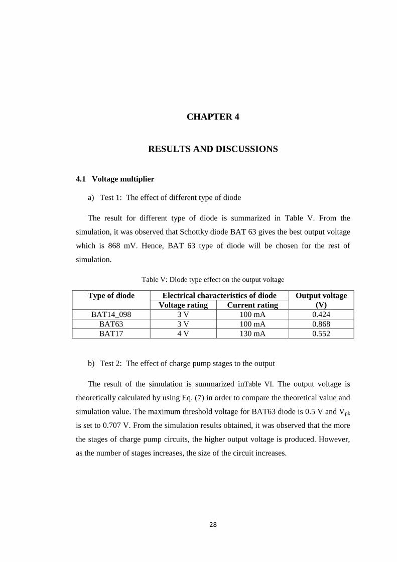
RESULTS AND DISCUSSIONS .............................................................................. 28
4.1 Voltage multiplier........................................................................................... 28
4.2 Current amplifier ............................................................................................ 32
4.3 Experimental result.......................................................................................... 33
CONCLUSION .......................................................................................................... 34
REFERENCES........................................................................................................... 35
APPENDICES ........................................................................................................... 37

vii
LIST OF TABLES
Table I: Comparison of power Density of energy harvesting methods ...................... 4
Table II: Literature review summary table ................................................................ 11
Table III: Summary of Milestone.............................................................................. 18
Table IV: List of tools ................................................................................................ 27
Table V: Diode type effect on the output voltage ...................................................... 28
Table VI : Stages number effect on the output voltage .............................................. 29
Table VIII : simulation vs. experimental result for voltage multiplier ...................... 33

viii
LIST OF FIGURES
Figure 1 Basic block diagram of RF energy harvesting .............................................. 6
Figure 2 Step of RF energy harvesting ....................................................................... 6
Figure 3: Spectrum of signals in the range from 100 KHz to 3 GHz [14] ................... 7
Figure 4 voltage multiplier circuit [9, 24] .................................................................. 10
Figure 5 Flow chart ................................................................................................... 15
Figure 6 Key milestones for FYP 1 .......................................................................... 16
Figure 7 Key milestones for FYP 2 .......................................................................... 17
Figure 8: Proposed block diagram of energy harvesting system ............................... 19
Figure 9: Basic design of charge pump ...................................................................... 20
Figure 10 Single stage charge pump with Schottky diode BAT14_098 .................... 21
Figure 11 Single stage charge pump with Schottky diode BAT63 ............................ 22
Figure 12 Single stage charge pump with Schottky diode BAT17 ............................ 22
Figure 13 : 3 Stages of charge pump circuit .............................................................. 23
Figure 14 : 5 Stages of charge pump circuit .............................................................. 23
Figure 15 : 7 Stages of charge pump circuit .............................................................. 24
Figure 16 : 9 Stages of charge pump circuit .............................................................. 24
Figure 17: 11 Stages of charge pump circuit ............................................................. 25
Figure 18: LT1763 micropower regulator circuit ...................................................... 25
Figure 19: voltage multiplier circuit on testing .......................................................... 26
Figure 20: Equipment setup ....................................................................................... 27
Figure 21 : Graph of output voltage vs number of stages of voltage multiplier ........ 29
Figure 22: Output waveform of 3 stages voltage multiplier ...................................... 30
Figure 23: Output waveform of 5 stages voltage multiplier ...................................... 30
Figure 24: Output waveform of 7 stages voltage multiplier ...................................... 30
Figure 25: Output waveform of 9 stages voltage multiplier ...................................... 31
Figure 26: Output waveform of 11 stages voltage multiplier .................................... 31
Figure 27: ripples at DC output voltage ..................................................................... 32
Figure 28 : Output waveform for LT1763 ................................................................. 33

ix
LIST OF ABBREVIATIONS
AC : Alternating Current
BSS : Base Station Subsystem
DC : Direct Current
GSM : Global System for Mobile
Hz : Hertz
IC : Integrated Circuit
LAN : Local Area Network
LDO : Low Drop Out
mAh : milliamp hours
NSS :Network and Switching Subsystem
OSS : Operation Support Subsystem
RF : Radio Frequency
W : Watt
WiMAX : Worldwide Interoperability for Microwave

1
CHAPTER 1
INTRODUCTION
1.1 Background of study
Nowadays mobile communication is one of the fast growing market tools and
widely used by people in all over the world. Throughout the year, cellular phone
technology is shrinking not only the ICs size but also the batteries. The need for
automatic charging technique is required instead of wired charging via USB or AC
socket. Recently there are lots of studies conducted about supplying power to
electronics devices using wireless power transmission technology. It is expected that
by eliminating the need for power cables, charging batteries can be done anywhere
without the need of power supply. Hence, most users do not have to worry that their
handheld devices to run out of battery anymore.
Energy harvesting is a conversion of ambient energy present in the
environment into electrical energy. There is an abundance of energy propagates all
around us at all times. There are some applications such as radio and television
towers, satellites orbiting earth and even the cellular phone antennas are constantly
transmitting energy. Energy can be harvested from sources such as vibrations,
thermal and RF (radio frequency) sources. RF is a general term used to encompass
the frequency within the electromagnetic spectrum in the range of about 3 kHz to
300 GHz [1], which corresponds to the frequency of radio waves and the alternating
currents to carry radio signal. The advent of wireless broadcasting and
communication has increased the availability of free RF energy. Harvesting ambient
energy would offer an alternate energy source for low power applications [2]. Global
system for mobile (GSM) is one example of energy present in RF range.
GSM is the second-generation cellular system standard or known as 2G.
GSM was developed to work out the fragmentation problems of the first cellular
systems. Recently, GSM system is the most popular digital cellular
2
telecommunications system and widely used in the world. The range of GSM system
utilizes within 25 MHz, 890-915 MHz and 935-960 MHz for transmitting and
receiving bands of the mobile system respectively [3].
1.2 Problem statement
The fast growing of wireless device and products in market has become the
most popular demand among the consumers. Unfortunately the wireless devices are
constrained in terms of their batteries due to the inability to operate independently of
centralized power sources for an unlimited duration. Nowadays, there have been
studies that discovered new method for wired battery charging problem such as
power bank and also by shrinking the charger in order to make it easier to carry
along with chargeable electronic devices. Although the charger becomes smaller, but
it still needs to be plugged into wall outlet.
As the wired charging method was inconvenient method, the better way to
transfer power is by wireless power transfer using energy harvesting method instead
of traditional methods using power cables. By eliminating the need for power cables,
most users do not have to worry in carrying along the charger during travel and also
in case of no power supply.
The project is addressed to implement wireless technique for battery charging
module. By having such development, mobile or tablet users do not have to worry
about finding AC outlet or USB port because the charging is done automatically
through novel energy harvesting technique. The aim is to use the harvested GSM
energy in order to supply electrical power in places where electrical energy sources
cannot be found. Therefore, users are able to get their handheld items powered up
wirelessly anywhere.
The availability of the GSM energy is the limitation of the project. The
energy levels that can be harvested in the environment are very low that no electronic
device can use them. Therefore the output voltage must be boosted before it can be
used to power up an electronics devices.
3
1.3 Objectives and scope of study
The main objective of this work is to improve the current wired battery charging
by developing new alternative technique using energy harvesting method. In
particular, this study aims:
a) to understand the basic principle of RF, GSM and operation of mobile
communication.
b) to design and simulate the converter to produce 3.7 V output voltage and
1.5 A output current for specific mobile or tablet load application.
c) to design and simulate the current amplifier circuit to increase the output
current.
d) to develop the voltage multiplier circuit and test the design.
1.4 Significance of the project
The project is significant in term of applying new method for battery
charging module. By using energy harvesting method, the charging can be done
automatically without need for power cable. At the same time the electricity
consumption can be reduced. Consequently, it provide an alternative source of the
energy especially in the current situation where the most of the energy produced
depends on non-renewable energy such as oil and gas sources.

4
CHAPTER 2
LITERATURE REVIEW
The idea of harvesting energy from ambient sources has been around since
the invention of piezoelectric materials [4]. The usable energy can be obtained from
piezoelectric materials by using simple electronic embedded in mobile phone to
convert into electrical energy. The recent studies [2, 4] have shown that energy could
also be harvested by the RF energy in the environment. The received radio energy
can be converted to DC by using rectifier and conversion technique then supplied
energy to the battery. Besides, researchers found that not only RF energy could be
harvested but also from various energy sources, such as mechanical vibrations,
electromagnetic sources, light, acoustic, airflow, heat and temperature variations. In
real situation, the energy transmitted by wireless sources is much higher, but only
small amount can be harvested in environment as the rest is converted into heat or
absorbed by other materials [5]. Table I shows the comparison of the estimated
power and challenges of various ambient energy sources in a recent study by [6].
Table I: Comparison of power Density of energy harvesting methods
Energy Source Power Density & Performance
Acoustic Noise 0.003 μW/cm3@75 db
0.96 μW/cm3 @ 100 db
Temperature Variation 10 μW/cm3
Ambient Radio Frequency 1 μW/cm2
Ambient Light 100 mW/cm2 (direct sun)
100 _W/cm2 (illuminated office)
Thermoelectric 60 _W/cm2
Vibration 4 _W/cm3 (human motion—Hz)

5
(micro generator) 800 _W/cm3 (machines—kHz)
Vibrations (Piezoelectric) 200 μW/cm3
Airflow 1 μW/cm2
Push buttons 50 _J/N
Hand generators 30 W/kg
Heel strike 7 W/cm2
Values in the Table I were derived from a combination of published studies, theory
and information from textbooks. Mostly the energy sources as shown in the Table I
are highly dependent on the application. Thermal energy for instance is limited
because differences on temperature across a chip are typically low [6].
2.1 Radio frequency (RF)
Radio frequency is present everywhere in the environment, in the form of signals
transmission from mobile phone (GSM), wireless LAN (WiFi, WiMAX), radio, TV,
Bluetooth, etc [5]. Study has been done in urban area in order to identify the density
of RF energy. From the experiment, it has been reported that RF energy density can
be as high as 0.5 µW/cm2 in urban area.
This value corresponds to an input power
level of 16.6 µW (-17.6 dBm) at 1800 MHz [7]. RF can be classified as one of the
categories of energy carrying wave which is identified in the electromagnetic
spectrum. RF and microwaves are two different types of electromagnetic waves. RF
has range of frequencies between 3 kHz to 300 GHz whilst microwaves frequencies
are between 300 MHz (0.3 GHz) to 300 GHz [8]. RF energy harvesting can be used
as alternate power source for low power applications such as battery charging in
mobile communication. Although this method is a good alternative for battery
charging, however there are several challenges to implement this method [2] :
a) Required high gain antenna for all frequency bands due to available power
varies with distance and gain of the receiver antenna.
b) Broadband impedance matching network is necessary for maximum power
transfer due to non linear dependence of the rectifier impedance on the
frequency and power.

6
c) It required higher efficiencies of RF-DC conversion and low power DC-DC
converter.
Figure 1 shows the basic block diagram of RF-DC conversion system. A good
design of RF energy harvesting system should reduce power dissipation by
minimizing the numbers of components [2].
Figure 1 Basic block diagram of RF energy harvesting
RF energy harvesting model is divided into three (3) subsystems. They are
receiving antenna subsystem, rectifying subsystem and energy storage subsystem.
Figure 2 shows the main step in harvesting method; transducer, energy conditioning
stage and energy storage unit [9, 10].
.
Figure 2 Step of RF energy harvesting
Transducer consists of antenna for converting RF energy to electrical form. The
transducer design should be efficient in order to convert more RF energy into the
system. Voltage doublers (charge pump) or voltage multiplier circuit is to amplify
the incoming signal in order to increase output voltage. The last component is energy

7
storage unit. As the incoming RF energy is not constant over the time, storage unit is
essential to fulfil the demand of the devices.
The amount of energy that could be harvested is required as an input for this
project. For this purpose, the actual amount is referred from previous study done by
some researchers. The value of energy that could be harvested in environment is
mentioned by [11] . A spectrum analyzer is used for this purpose. However the
output power of RF is limited by some regulations due to safety and health concern
offered by EM radiations. According to [12], the maximum theoretical power
available for RF energy harvesting in distance 40 meters is about 7.0 µW and 1.0 µW
for 900 MHz and 2.4 GHz respectively. The power available in the environment is
estimated around 50 mW to 100 mW. However the energy that could be harvested
from environment is about 10 µW to 100 µW [13]. 250 mW energy can be harvested
from electro-magnetic noise generated from a fluorescent lamp while 60 µW of RF
energy was harvested from TV tower. Figure 3 shows the spectrum of RF signals
existing in frequency range of 100 KHz to 3 GHz at a distance of 400 m.
Figure 3: Spectrum of signals in the range from 100 KHz to 3 GHz [14]
As can be observed from Figure 3, there are different values of power at
different ranges of frequencies. The signals in frequency within 950 MHz to 960
MHZ experienced more power and less hopping than other frequency range [15].
The amount of received power actually depends on the distance decay, which can be
calculated as stated in Eq. (1):

8
𝑊𝑎 =𝜆2
4𝜋𝑧 𝐺𝑎𝑡 𝐺𝑎𝑟𝑊𝑡 (1)
where 𝑊𝑎 , λ, 𝑧, 𝐺𝑎𝑡 , 𝐺𝑎𝑟 and 𝑊𝑡 are received RF power, the wavelength, the distance
between the transmitter and receiver, the transmitter antenna gain, the receiver
antenna gain, and transmission power respectively.
However, ambient energy sources are usually unstable and cannot be
harvested during a certain period of time. For instance, RF energy from TV
broadcasts can obtain power all day except during the maintenance period. The
actual value of energy harvested from TV broadcasts could not be estimated properly
because the RF power attenuated due to the multipath effect, reflection, shielding
object, etc. The study done by [11] shows that the amount of harvested power
decreases every day at midnight, i.e. from around 1:00 a.m. to 6:00 a.m. due to
maintenance factor.
2.2 Global system for mobile (GSM)
Early GSM cellular phone has some weaknesses in terms of the battery
management which could only allow for less than an hour of talk time [16]. Hence,
second generation of GSM cellular system standard purposely developed to improve
the limitation of first cellular system. The system was put forward into European
since 1991 [3]. According to [3], there are three major subsystems of the GSM
network architecture: Base Station Subsystem BSS, Network and Switching
Subsystem NSS and operation support Subsystem OSS. There are five parts of GSM
services which include internet, mobile fax, secure corporate, LAN access, cell
broadcast, and short message. According to [14], the power of air signals can be as
high as 30 dBm for GSM frequency which is relatively high and can be used for low
power application. For GSM-900 mobile phone, a scavenged power of 1.9 mW is
predicted at a distance of 1 m [17].
2.3 Antenna
Previous researchers have done the survey to find out the availability of RF
signal by using spectrum analyser and antenna. They have found that RF signal are
widely available in GSM (global system for mobile communication) band with

9
frequency between 890 MHz – 960 MHz. Hence, antenna is used since the RF
energy is available in form of electromagnetic waves [9]. It works as converter which
converts energy in to electrical form besides of transmitting and receiving signal.
There are 3 types of antenna that commonly used: monopole, dipole and micro strip
antenna [18]. Most of antenna in rectenna application uses micro strip patch antenna
instead of monopole and dipole antenna because micro strip antenna is most efficient
since it has less loss and small in size. ―Rectenna‖ is short name for rectifying
antenna that used to capture and convert RF or microwave power to DC power. The
efficiency of RF to DC conversion (ηRF to DC) can be calculated according to the
following definitions [19] as given by Eq. (2) and Eq. (3) :
𝜂𝑅𝐹 𝑡𝑜 𝐷𝐶, 𝑟𝑒𝑐𝑡𝑒𝑛𝑛𝑎 =𝑃𝑂𝑈𝑇 ,𝐷𝐶
𝑆𝑅𝐹𝐴𝐺=
𝑉2𝐷𝐶
𝑅𝐿𝑂𝐴𝐷
1
𝑆𝑅𝐹𝐴𝐺 (2)
𝜂𝑅𝐹 𝑡𝑜 𝐷𝐶,𝑅𝑒𝑐𝑡𝑖𝑓𝑖𝑒𝑟 = 𝑃𝑂𝑈𝑇 ,𝐷𝐶
𝑃𝑅𝐼𝐶 ,𝑅𝐹=
𝑉2𝐷𝐶
𝑅𝐿𝑂𝐴𝐷
1
𝑆𝑅𝐹𝐴𝑒𝑓𝑓 (3)
where 𝑆𝑅𝐹 is the power density incident on the antenna, VDC is the DC output
voltage, 𝑅𝐿𝑂𝐴𝐷 is resistive load, 𝐴𝐺 is the geometric area of the antenna and 𝐴𝑒𝑓𝑓 is
its effective area. The aim of the formula given in Eq. (2) is to emphasize the
efficiency of the antenna in collecting the electromagnetic radiation. RF to DC
conversion efficiency of rectifier is given in Eq. (3).
Other type of antenna to consider is known as patches. This type of antenna
have two major problems analyzed by [20] where it needs to be quite large in size.
Second problem is that it is highly directional; meaning that it will receive radiation
in one direction. In order to increase the power/area ratio, multiple energy harvesting
antennas in one area was proposed and studied by [21, 22]. The studies found that as
the area increases, the power generated is also increasing.
2.4 Charge pump/ voltage multiplier rectifier circuit
The energy levels that can be harvested in the environment are so low that no
electronic device can use them. Output voltage must be boosted before it can be used
to power electronics devices [23]. The researcher found that the maximum
theoretical power available for energy harvesting is 7.0 µW for 900 MHz frequency
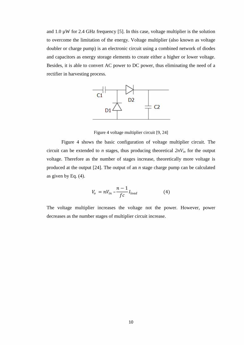
10
and 1.0 µW for 2.4 GHz frequency [5]. In this case, voltage multiplier is the solution
to overcome the limitation of the energy. Voltage multiplier (also known as voltage
doubler or charge pump) is an electronic circuit using a combined network of diodes
and capacitors as energy storage elements to create either a higher or lower voltage.
Besides, it is able to convert AC power to DC power, thus eliminating the need of a
rectifier in harvesting process.
Figure 4 voltage multiplier circuit [9, 24]
Figure 4 shows the basic configuration of voltage multiplier circuit. The
circuit can be extended to n stages, thus producing theoretical 2nVin for the output
voltage. Therefore as the number of stages increase, theoretically more voltage is
produced at the output [24]. The output of an n stage charge pump can be calculated
as given by Eq. (4).
𝑉𝑜 = 𝑛𝑉𝑖𝑛 –𝑛 − 1
𝑓𝑐𝐼𝑙𝑜𝑎𝑑 (4)
The voltage multiplier increases the voltage not the power. However, power
decreases as the number stages of multiplier circuit increase.
11
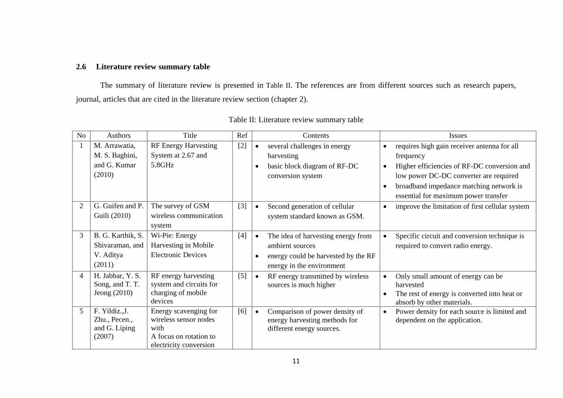
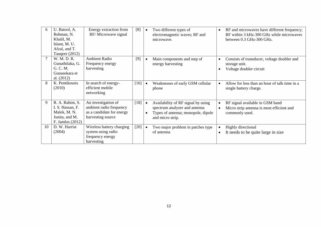
2.6 Literature review summary table
The summary of literature review is presented in Table II. The references are from different sources such as research papers,
journal, articles that are cited in the literature review section (chapter 2).
Table II: Literature review summary table
No Authors Title Ref Contents Issues
1 M. Arrawatia,
M. S. Baghini,
and G. Kumar
(2010)
RF Energy Harvesting
System at 2.67 and
5.8GHz
[2] several challenges in energy
harvesting
basic block diagram of RF-DC
conversion system
requires high gain receiver antenna for all
frequency
Higher efficiencies of RF-DC conversion and
low power DC-DC converter are required
broadband impedance matching network is
essential for maximum power transfer
2 G. Guifen and P.
Guili (2010)
The survey of GSM
wireless communication
system
[3] Second generation of cellular
system standard known as GSM.
improve the limitation of first cellular system
3 B. G. Karthik, S.
Shivaraman, and
V. Aditya
(2011)
Wi-Pie: Energy
Harvesting in Mobile
Electronic Devices
[4] The idea of harvesting energy from
ambient sources
energy could be harvested by the RF
energy in the environment
Specific circuit and conversion technique is
required to convert radio energy.
4 H. Jabbar, Y. S.
Song, and T. T.
Jeong (2010)
RF energy harvesting
system and circuits for
charging of mobile
devices
[5] RF energy transmitted by wireless
sources is much higher
Only small amount of energy can be
harvested
The rest of energy is converted into heat or
absorb by other materials.
5 F. Yildiz.,J.
Zhu., Pecen.,
and G. Liping
(2007)
Energy scavenging for
wireless sensor nodes
with
A focus on rotation to
electricity conversion
[6] Comparison of power density of
energy harvesting methods for
different energy sources.
Power density for each source is limited and
dependent on the application.
12
6 U. Batool, A.
Rehman, N.
Khalil, M.
Islam, M. U.
Afzal, and T.
Tauqeer (2012)
Energy extraction from
RF/ Microwave signal
[8] Two different types of
electromagnetic waves; RF and
microwave.
RF and microwaves have different frequency;
RF within 3 kHz-300 GHz while microwaves
between 0.3 GHz-300 GHz.
7 W. M. D. R.
Gunathilaka, G.
G. C. M.
Gunasekara et
al. (2012)
Ambient Radio
Frequency energy
harvesting
[9] Main components and step of
energy harvesting
Consists of transducer, voltage doubler and
storage unit.
Voltage doubler circuit
8 K. Pentikousis
(2010)
In search of energy-
efficient mobile
networking
[16] Weaknesses of early GSM cellular
phone
Allow for less than an hour of talk time in a
single battery charge.
9 R. A. Rahim, S.
I. S. Hassan, F.
Malek, M. N.
Junita, and M.
F. Jamlos (2012)
An investigation of
ambient radio frequency
as a candidate for energy
harvesting source
[18] Availability of RF signal by using
spectrum analyzer and antenna
Types of antenna; monopole, dipole
and micro strip.
RF signal available in GSM band
Micro strip antenna is most efficient and
commonly used.
10 D. W. Harrist
(2004)
Wireless battery charging
system using radio
frequency energy
harvesting
[20] Two major problem in patches type
of antenna
Highly directional
It needs to be quite large in size
13
CHAPTER 3
METHODOLOGY
3.1 Procedures
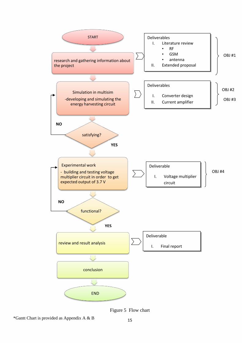
This project shall include three execution phases as described below. The summary
for project activities is summarized in flow chart as shown in Figure 5.
3.1.1 Research and literature review
In the early stage of the project, literature review has to be done in order to
get an insight and understanding energy harvesting method. The study also
emphasizes on the basic concepts of radio frequency propagation, global system for
mobile application and mobile network communication. The important point and
basic understanding has been established as described in Chapter 2. Review must be
done to get as much understanding as possible from research papers, journals,
articles, and other sources available on internet. Attention shall be given to two
components, which are the conversion circuit and amplifier circuit.
3.1.2 Designing and simulation the circuit
Conversion circuit consisting of voltage multiplier rectifier is designed to
achieve charging output voltage of 3.7 V. Then amplifier circuit is another important
circuit designed to increase the output current for the load to meet the requirement of
1.5 A load. These two circuit models will be analyzed with the use of circuit
simulation software such as Multisim 12.0. If the simulation results are incorrect,
improvement in the circuit design should be carried out. When required simulation
results are obtained, list of components and devices will be identified for fabrication.
3.1.3 Testing and Prototyping
The fabrication of voltage multiplier will be done and testing is required to
validate the functionality of the prototype. During the testing, the input is fed by

14
signal generator or AC power transformer using generic value of input
voltage getting from previous research. It will be used as reference throughout this
project. The output is monitored by using multimeter and the result is analysed. If the
testing phase meets the requirement, the result analysis will be then carried out. The
analysis on how to have better outcome is carried out consequently. Besides,
recommendation is made for further improvement in the future design.
15
Figure 5 Flow chart
START
research and gathering information about the project
Simulation in multisim
-developing and simulating the energy harvesting circuit
satisfying?
Experimental work
- building and testing voltage multiplier circuit in order to get expected output of 3.7 V
functional?
review and result analysis
conclusion
END
Deliverables I. Literature review
• RF • GSM • antenna
II. Extended proposal
Deliverables
I. Converter design
II. Current amplifier
Deliverable
I. Voltage multiplier
circuit
Deliverable
I. Final report
OBJ #1
OBJ #2
OBJ #3
OBJ #4
NO
YES
NO
YES
*Gantt Chart is provided as Appendix A & B
16
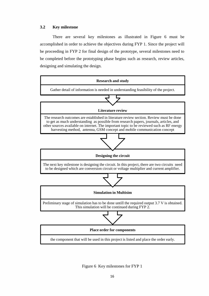
3.2 Key milestone
There are several key milestones as illustrated in Figure 6 must be
accomplished in order to achieve the objectives during FYP 1. Since the project will
be proceeding in FYP 2 for final design of the prototype, several milestones need to
be completed before the prototyping phase begins such as research, review articles,
designing and simulating the design.
Figure 6 Key milestones for FYP 1
Place order for components
the component that will be used in this project is listed and place the order early.
Simulation in Multisim
Preliminary stage of simulation has to be done untill the required output 3.7 V is obtained. This simulation will be continued during FYP 2.
Designing the circuit
The next key milestone is designing the circuit. In this project, there are two circuits need to be designed which are conversion circuit or voltage multiplier and current amplifier.
Literature review
The research outcomes are established in literature review section. Review must be done to get as much understanding as possible from research papers, journals, articles, and
other sources available on internet. The important topic to be reviewed such as RF energy harvesting method, antenna, GSM concept and mobile communication concept
Research and study
Gather detail of information is needed in understanding feasibility of the project.
17
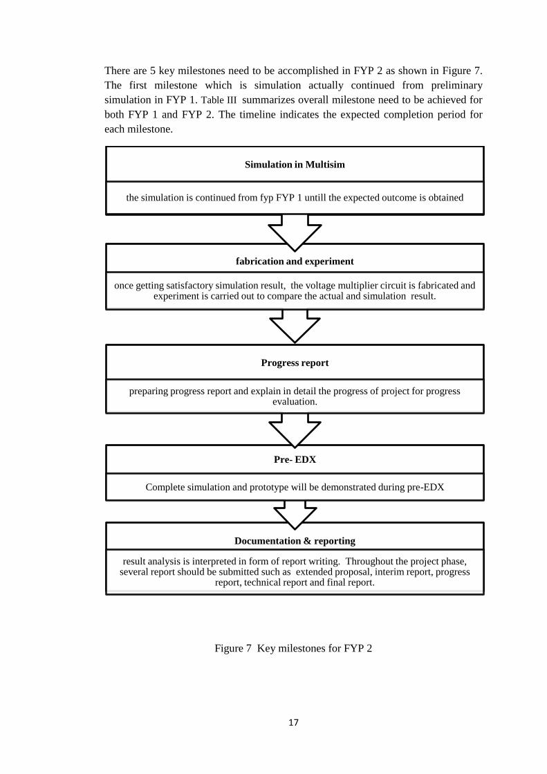
There are 5 key milestones need to be accomplished in FYP 2 as shown in Figure 7.
The first milestone which is simulation actually continued from preliminary
simulation in FYP 1. Table III summarizes overall milestone need to be achieved for
both FYP 1 and FYP 2. The timeline indicates the expected completion period for
each milestone.
Figure 7 Key milestones for FYP 2
Documentation & reporting
result analysis is interpreted in form of report writing. Throughout the project phase, several report should be submitted such as extended proposal, interim report, progress
report, technical report and final report.
Pre- EDX
Complete simulation and prototype will be demonstrated during pre-EDX
Progress report
preparing progress report and explain in detail the progress of project for progress evaluation.
fabrication and experiment
once getting satisfactory simulation result, the voltage multiplier circuit is fabricated and experiment is carried out to compare the actual and simulation result.
Simulation in Multisim
the simulation is continued from fyp FYP 1 untill the expected outcome is obtained

18
Table III: Summary of Milestone
MILESTONE
MONTH (2013/2014)
MAY ’13
JUNE ’13
JULY ’13
AUG ’13
SEPT ’13
OCT ’13
NOV ’13
DEC ’13
JAN ‘14
Understanding the project
principle
Design converter and current
amplifier circuit
Preliminary simulation of the
circuit design
Experiments, data collection and
analysis
Project presentation and
evaluation
Final Report writing
Project completion

19
3.3 Proposed Topology
Figure 8 illustrates the proposed block diagram of energy harvesting
technique in order to power up the load.
Figure 8: Proposed block diagram of energy harvesting system
The conversion circuit consists of charge pump used to achieve the charging
output voltage that is suitable to charge mobile phone. Hence, the specification of
battery is required in this project in order to know the battery requirement for
charging. The battery specifications are as follow:
i. Battery type: Lithium-ion
ii. Nominal voltage: 3.7 V
iii. Charge current: 0.5 A
iv. Discharge current: 1 A
v. Capacity: 1600 mAh
Since the nominal voltage for battery is 3.7 V, the charge pump shall be designed to
increase the output voltage up to 3.7 V.
3.3.1 Charge pump/ voltage multiplier
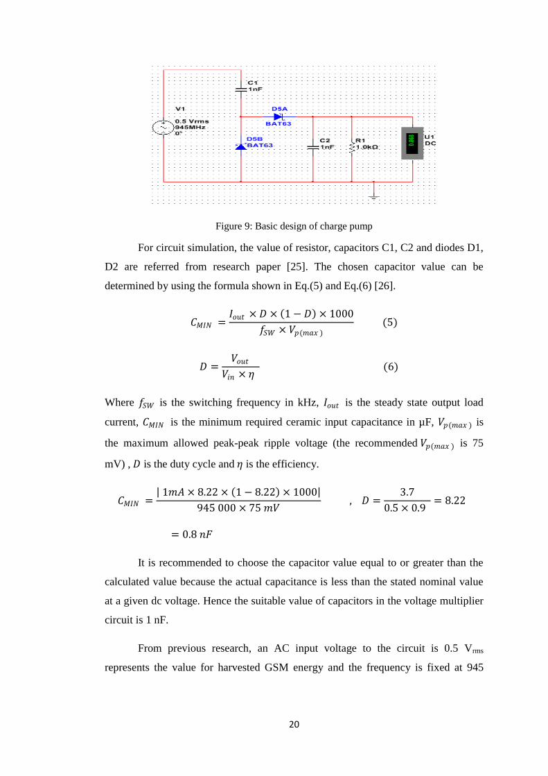
Figure 9 shows the basic design of charge pump simulated in Multisim.
Simulation has been done for better understanding of the voltage multiplier circuits
which functions as transformers in order to increase the output voltage. The output of
the charge pump is measured by DC multimeter. The simulation for charge pump is
focused on determining the most efficient values of the capacitors (number of stages)
in the charge pumps and the suitable type of diode to be used as described in section
4.1.
GSM energy
Voltage Multiplier
(Conversion circuit)
Current amplifier
Load (Battery)
20
Figure 9: Basic design of charge pump
For circuit simulation, the value of resistor, capacitors C1, C2 and diodes D1,
D2 are referred from research paper [25]. The chosen capacitor value can be
determined by using the formula shown in Eq.(5) and Eq.(6) [26].
𝐶𝑀𝐼𝑁 =𝐼𝑜𝑢𝑡 × 𝐷 × 1 − 𝐷 × 1000
𝑓𝑆𝑊 × 𝑉𝑝(𝑚𝑎𝑥 ) (5)
𝐷 =𝑉𝑜𝑢𝑡
𝑉𝑖𝑛 × 𝜂 (6)
Where 𝑓𝑆𝑊 is the switching frequency in kHz, 𝐼𝑜𝑢𝑡 is the steady state output load
current, 𝐶𝑀𝐼𝑁 is the minimum required ceramic input capacitance in µF, 𝑉𝑝(𝑚𝑎𝑥 ) is
the maximum allowed peak-peak ripple voltage (the recommended 𝑉𝑝(𝑚𝑎𝑥 ) is 75
mV) , 𝐷 is the duty cycle and 𝜂 is the efficiency.
𝐶𝑀𝐼𝑁 = 1𝑚𝐴 × 8.22 × 1 − 8.22 × 1000
945 000 × 75 𝑚𝑉 , 𝐷 =
3.7
0.5 × 0.9 = 8.22
= 0.8 𝑛𝐹
It is recommended to choose the capacitor value equal to or greater than the
calculated value because the actual capacitance is less than the stated nominal value
at a given dc voltage. Hence the suitable value of capacitors in the voltage multiplier
circuit is 1 nF.
From previous research, an AC input voltage to the circuit is 0.5 Vrms
represents the value for harvested GSM energy and the frequency is fixed at 945
21
MHz, the performance of the circuit with different number of stages were observed
and analysed to choose the maximum output delivered to the load.
The output voltage can be calculated theoretically as shown in Eq.(7). There
will be a small difference between theoretical value and simulated output as a result
of the parasitic capacitances of the diode and the saturation current.
𝑉𝑜𝑢𝑡 = 2𝑁(𝑉𝑝𝑘 − 𝑉𝑡ℎ) (7)
where 𝑉𝑝𝑘 is 2 𝑉𝑟𝑚𝑠 , 𝑁 is number of stage, and 𝑉𝑡ℎ is threshold voltage for diode.
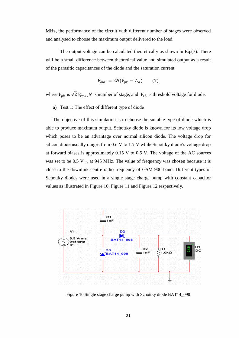
a) Test 1: The effect of different type of diode
The objective of this simulation is to choose the suitable type of diode which is
able to produce maximum output. Schottky diode is known for its low voltage drop
which poses to be an advantage over normal silicon diode. The voltage drop for
silicon diode usually ranges from 0.6 V to 1.7 V while Schottky diode’s voltage drop
at forward biases is approximately 0.15 V to 0.5 V. The voltage of the AC sources
was set to be 0.5 Vrms at 945 MHz. The value of frequency was chosen because it is
close to the downlink centre radio frequency of GSM-900 band. Different types of
Schottky diodes were used in a single stage charge pump with constant capacitor
values as illustrated in Figure 10, Figure 11 and Figure 12 respectively.
Figure 10 Single stage charge pump with Schottky diode BAT14_098
22
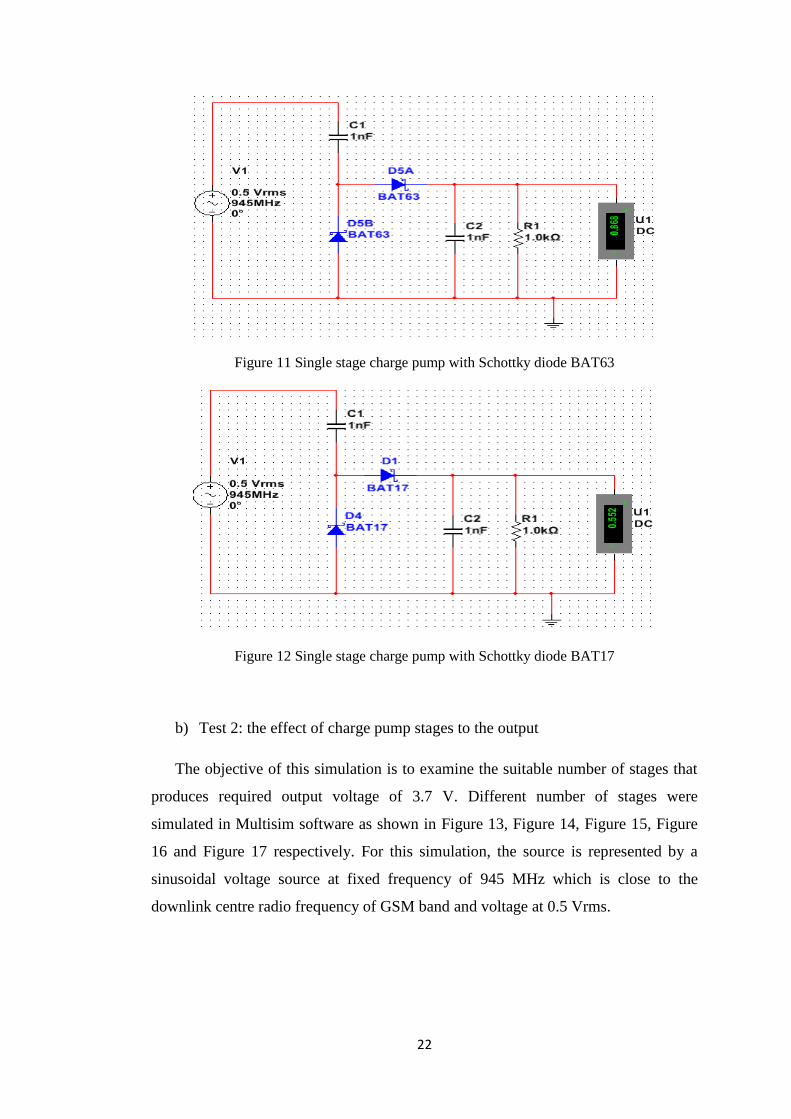
Figure 11 Single stage charge pump with Schottky diode BAT63
Figure 12 Single stage charge pump with Schottky diode BAT17
b) Test 2: the effect of charge pump stages to the output
The objective of this simulation is to examine the suitable number of stages that
produces required output voltage of 3.7 V. Different number of stages were
simulated in Multisim software as shown in Figure 13, Figure 14, Figure 15, Figure
16 and Figure 17 respectively. For this simulation, the source is represented by a
sinusoidal voltage source at fixed frequency of 945 MHz which is close to the
downlink centre radio frequency of GSM band and voltage at 0.5 Vrms.

23
Figure 13 : 3 Stages of charge pump circuit
Figure 14 : 5 Stages of charge pump circuit

24
Figure 15 : 7 Stages of charge pump circuit
Figure 16 : 9 Stages of charge pump circuit

25
Figure 17: 11 Stages of charge pump circuit
Since the required output voltage is achieved at eleventh stages of charge
pump, the current is measured at the output as shown in Figure 17 in order to know
the period for battery to fully charge.
3.3.2 Current amplifier
The circuit simulation in Figure 17 shows that the output current at eleventh
stages of charge pump is too small. Hence the current need to be increased in order to
charge the battery for shorter period. The LT1763 series low dropout regulator is
used for this purpose.
Figure 18: LT1763 micropower regulator circuit

26
The LT1763 series are micropower, low dropout (LDO) regulator that
capable to supply 500mA of output current with a dropout voltage of 300mV. This
device can be found in many applications such as cellular phone, battery-powered
system and noise-sensitive instrumentation system. Figure 18 shows the pinout
configuration for LT 1763 in order to increase the output current. The input voltage
V1 is referred to output voltage of 11th
stages of voltage multiplier circuit. The value
of C1, C2 and C3 are taken from component datasheet that is provided in appendix D
while R1 is example of load resistor. The LT1763 series come in fixed output
voltages of 1.5 V, 1.8 V, 2.5 V, 3.3 V and 5 V. In this project, LT1763CS8-5 is used
in order to get the maximum output voltage of 5 V.
3.4 Experimental setup
The experiment was carried out using direct AC input generated from
regulated AC power transformer. This part of experiment is to verify that the voltage
multiplier circuit works as specified in theory and simulation.
Voltage multiplier circuit was tested on the board as shown in Figure 19. Due
to the unavailability of BAT63 Schottky diode, the initial design utilized the
germanium diode based on the fact that Germanium diode also has low voltage drop
of 0.3 V. The datasheet for OA 90 germanium diode can be found in the appendix C.
The circuit consists of OA 90 germanium diode, 1 nF capacitor, 1 kΩ resistor and
wire.
Figure 19: voltage multiplier circuit on testing

27
Figure 20: Equipment setup
The equipment setup for the experiment is shown in Figure 20. An Ac power
transformer was regulated to 0.5 Vac as input voltage for voltage multiplier circuit.
This value is generic representation of an AC signal for GSM energy that is
harvested from the surrounding. The multimeter reading of output voltage is
tabulated in section 4.3.
3.5 List of tools
Several software and hardware equipment were utilized to achieve the project’s goal
as shown in Table IV.
Table IV: List of tools
No. Name of component Manufacturer/
supplier Qty
Price/unit
(RM)
Total price
(RM)
1 Germanium diode
(OA 90) RS Components 15 2.554 38.31
2 Donut board
20x8.5 cm Cytron 1 15.00 15.00
3 Capacitor (1 nF) EE store 12 - -
4 Resistor (1 Ω) EE store 2 - -
6 NI Multisim 12.0 Downloaded N/A N/A N/A
TOTAL (RM) 53.31
Lab equipments:
Function generator, Fluke Multimeter, AC power transformer, and Solder
tools.
28
CHAPTER 4
RESULTS AND DISCUSSIONS
4.1 Voltage multiplier
a) Test 1: The effect of different type of diode
The result for different type of diode is summarized in Table V. From the
simulation, it was observed that Schottky diode BAT 63 gives the best output voltage
which is 868 mV. Hence, BAT 63 type of diode will be chosen for the rest of
simulation.
Table V: Diode type effect on the output voltage
Type of diode Electrical characteristics of diode Output voltage
(V) Voltage rating Current rating
BAT14_098 3 V 100 mA 0.424
BAT63 3 V 100 mA 0.868
BAT17 4 V 130 mA 0.552
b) Test 2: The effect of charge pump stages to the output
The result of the simulation is summarized inTable VI. The output voltage is
theoretically calculated by using Eq. (7) in order to compare the theoretical value and
simulation value. The maximum threshold voltage for BAT63 diode is 0.5 V and Vpk
is set to 0.707 V. From the simulation results obtained, it was observed that the more
the stages of charge pump circuits, the higher output voltage is produced. However,
as the number of stages increases, the size of the circuit increases.
29
Table VI : Stages number effect on the output voltage
Number
of
stages
Output voltage (V)
Output
current
(mA)
Power loss
(mW)
Calculation
Simulation
Percentage
differences
(%)
Simulation Calculation
= 𝐼2 × 𝑅
𝑉𝑜𝑢𝑡
= 2𝑁(𝑉𝑝𝑘− 𝑉𝑡ℎ)
3 1.242 1.643 26 1.41 1.98
5 2.07 2.340 13 2.36 5.56
7 2.898 3.035 4 3.04 9.24
9 3.726 3.670 1.5 3.78 14.29
11 4.554 4.25 6.7 4.25 18.06
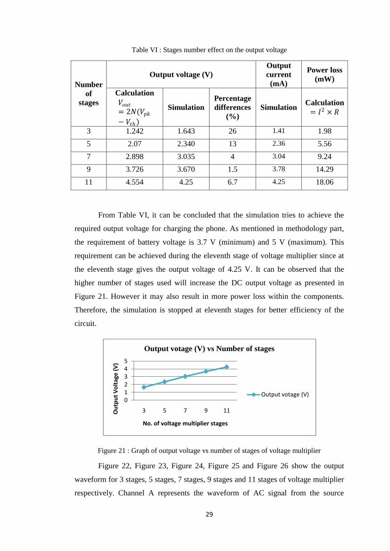
From Table VI, it can be concluded that the simulation tries to achieve the
required output voltage for charging the phone. As mentioned in methodology part,
the requirement of battery voltage is 3.7 V (minimum) and 5 V (maximum). This
requirement can be achieved during the eleventh stage of voltage multiplier since at
the eleventh stage gives the output voltage of 4.25 V. It can be observed that the
higher number of stages used will increase the DC output voltage as presented in
Figure 21. However it may also result in more power loss within the components.
Therefore, the simulation is stopped at eleventh stages for better efficiency of the
circuit.
Figure 21 : Graph of output voltage vs number of stages of voltage multiplier
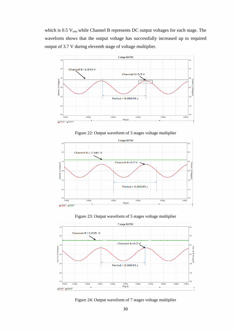
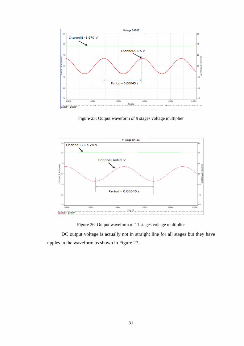
Figure 22, Figure 23, Figure 24, Figure 25 and Figure 26 show the output
waveform for 3 stages, 5 stages, 7 stages, 9 stages and 11 stages of voltage multiplier
respectively. Channel A represents the waveform of AC signal from the source
012345
3 5 7 9 11Ou
tpu
t V
olt
age
(V
)
No. of voltage multiplier stages
Output votage (V) vs Number of stages
Output votage (V)
30
which is 0.5 Vrms while Channel B represents DC output voltages for each stage. The
waveform shows that the output voltage has successfully increased up to required
output of 3.7 V during eleventh stage of voltage multiplier.
Figure 22: Output waveform of 3 stages voltage multiplier
Figure 23: Output waveform of 5 stages voltage multiplier
Figure 24: Output waveform of 7 stages voltage multiplier
31
Figure 25: Output waveform of 9 stages voltage multiplier
Figure 26: Output waveform of 11 stages voltage multiplier
DC output voltage is actually not in straight line for all stages but they have
ripples in the waveform as shown in Figure 27.

32
Figure 27: ripples at DC output voltage
4.2 Current amplifier
As described in section 3.3.2, LT1763 low dropout micropower voltage
regulator is simulated to increase the output current. By using LT1763, it can be
observed that the output current can be increased while the output voltage is slightly
decreasing due to 300 mV dropout voltage characteristic of the LT1763 series. The
simulation of LT1763CS8-5 as shown in section 3.3.2 shows that the regulator is
able to increase the current up to 800 mA and gives the output voltage of 4.231 V if
no load connected at the output. Hence by using this circuit, it can decrease the
charging period for the battery. For example, if the battery capacity is 1600 mAh, it
can fully charge within two hours if the current output of the regulator is 800 mA.
The circuit is tested with the load connected at the output to measure the new output
with the load present. For the simulation purpose, 4.7 ohm load resistor is connected
at the output as a load. As a result, the voltage produced at the output is 3.80 V which
is indicates the minimum output voltage of the regulator circuit. The special
characteristic of this regulator is limiting the output voltage up to 5 V maximum,
means that for any voltage enter the regulator (input voltage) that is exceed 5 V, the
output produced by this regulator is still fixed to 5 V. Hence, it is suitable to battery
charging and prevents any over voltage to occur although the input fed into regulator
is higher than 5 V. The output DC current waveform is shown in Figure 28.

33
Figure 28 : Output waveform for LT1763
4.3 Experimental result
The simulation and experimental findings of voltage multiplier is tabulated in Table
VII.
Table VII : simulation vs. experimental result for voltage multiplier
Number of stages
DC Output voltage (V)
Simulation Experiment
Differences
(|simulation-
experiment|) 3 1.643 0.930 0.713
5 2.340 1.296 1.044
7 3.035 2.720 0.315
9 3.670 2.960 0.71
11 4.250 3.975 0.275
From the experiment, it is verified that the voltage multiplier can be used to
increase the output voltage. The experimental value is slightly different with
simulation due to the different type of diode is used during the experiment. The
germanium diode is used instead of Schottky diode due to the unavailability of BAT
63 Schottky diode. Although the different type of diode is used, the diode rating does
not vary that much. However, the differences not give as much effect to the actual
required output since the chosen germanium diode having quite similar
characteristics with BAT 63.

34
CHAPTER 5
CONCLUSION
For overall, this project is presented as having three implementation phases.
Further research and study has been carried out in first phase, thus give an idea for
circuit designing and simulation in second phase. From the circuit simulation done in
Multisim 12.0, it shows that the load requirement of 3.7 V can be achieved at
eleventh stage of voltage multiplier circuit. BAT63 silicon schottky diode is used
since it gives the best output voltage rather than other type of diode, very small in
size and low threshold voltage level. The simulation shows that the output voltage at
eleventh stage voltage multiplier is 4.2 V with low output current. Hence the current
amplifier circuit is added at the voltage multiplier in order to increase the output
current.
In this project, LT1763 low dropout micropower regulator is chosen for
current amplifier circuit which can increases the current up to 800 mA and gives the
stable DC output voltage for maximum of 5 V. Based on the fact that it is capable to
limit the output voltage for maximum 5 V, the over voltage phenomena can be
avoided. The output voltage of eleventh stage voltage multiplier is slightly decreased
to 3.8 V when it is passing through current amplifier due to dropout voltage
characteristic of LT 1763.
As a conclusion, the objectives are successfully achieved by designing
eleventh stages of voltage multiplier and current amplifier circuit with the output
voltage and current of 4.2 V and 809 mA respectively. By using these results it can
say that it is possible to charge the battery using GSM energy that can be harvested
in the surrounding. In the future work, the actual prototype by using phone battery
will be demonstrated to show the real project achievement. Besides, the circuit
should be small in size in order to be fabricated in the phone.

35
REFERENCES
[1] K. Classic. (2011). Radiofrequency (RF) Radiation. Available:
http://hps.org/hpspublications/articles/rfradiation.html
[2] M. Arrawatia, M. S. Baghini, and G. Kumar, "RF Energy Harvesting System
at 2.67 and 5.8GHz," in Microwave Conference Proceedings (APMC), 2010
Asia-Pacific, pp. 900-903, 2010.
[3] G. Guifen and P. Guili, "The survey of GSM wireless communication
system," in Computer and Information Application (ICCIA), 2010
International Conference on, pp. 121-124, 2010.
[4] B. G. Karthik, S. Shivaraman, and V. Aditya, "Wi-Pie: Energy Harvesting in
Mobile Electronic Devices," in Global Humanitarian Technology Conference
(GHTC), 2011 IEEE, pp. 398-401, 2011.
[5] H. Jabbar, Y. S. Song, and T. T. Jeong, "RF energy harvesting system and
circuits for charging of mobile devices," Consumer Electronics, IEEE
Transactions on, vol. 56, pp. 247-253, 2010.
[6] F. Yildiz., J. Zhu., Pecen., and G. Liping., "Energy Scavenging For Wireless
Sensor Nodes With A Focus On Rotation To Electricity Conversion," 2007.
[7] L. Bo, S. Xi, N. Shahshahan, N. Goldsman, T. S. Salter, and G. M. Metze,
"Antenna-coupled dual band RF energy harvester design," in Semiconductor
Device Research Symposium (ISDRS), 2011 International, pp. 1-2, 2011.
[8] U. Batool, A. Rehman, N. Khalil, M. Islam, M. U. Afzal, and T. Tauqeer,
"Energy extraction from RF/ Microwave signal," in Multitopic Conference
(INMIC), 2012 15th International, pp. 165-170, 2012.
[9] W. M. D. R. Gunathilaka, G. G. C. M. Gunasekara, H. G. C. P. Dinesh, K. M.
M. W. N. Narampanawe, and J. V. Wijayakulasooriya, "Ambient Radio
Frequency energy harvesting," in Industrial and Information Systems (ICIIS),
2012 7th IEEE International Conference on, pp. 1-5, 2012.
[10] P. Nintanavongsa, U. Muncuk, D. R. Lewis, and K. R. Chowdhury, "Design
Optimization and Implementation for RF Energy Harvesting Circuits,"
Emerging and Selected Topics in Circuits and Systems, IEEE Journal on, vol.
2, pp. 24-33, 2012.
[11] H. Nishimoto, Y. Kawahara, and T. Asami, "Prototype implementation of
ambient RF energy harvesting wireless sensor networks," in Sensors, 2010
IEEE, pp. 1282-1287, 2010.
[12] N. Md. Din, C. K. Chakrabarty, A. B. Ismail, K. K. A. Devi, and W.Y.Chen,
"Design of Energy Harvesting System for Energizing Low Power Devices,"
Prgress In Electromagnetics Research, vol. 132, pp. 49-69, 2012.

36
[13] Tune In, Charge Up: Energy Harvesting Shows its Potetial. Available:
http://www.digikey.com/us/en/techzone/energy-
harvesting/resources/articles/tune-in-charge-up-rf-energy-harvesting.html
[14] M. Asefi, S. H. Nasab, L. Albasha, and N. Qaddoumi, "Energizing low power
circuits by using an RF signal harvester," vol. 16th Telecommunications
Forum TELFOR, Nov. 2008.
[15] N. Md. Din, C. K. Chakrabarty, A. Bin Ismail, K. K. A. Devi, and W.-Y.
Chen, "Design of RF energy harvesting system for energizing low power
devices," Progress In Electromagnetics Research, vol. 105, 273-294, 2012.
[16] K. Pentikousis, "In search of energy-efficient mobile networking,"
Communications Magazine, IEEE, vol. 48, pp. 95-103, 2010.
[17] H. J. Visser, A. C. F. Reniers, and J. A. C. Theeuwes, "Ambient RF Energy
Scavenging: GSM and WLAN Power Density Measurements," Microwave
Conference, 2008. EuMC 2008. 38th European, pp. 721-724, 2008.
[18] R. A. Rahim, S. I. S. Hassan, F. Malek, M. N. Junita, and M. F. Jamlos, "An
investigation of ambient radio frequency as a candidate for energy harvesting
source," in Industrial Electronics and Applications (ISIEA), 2012 IEEE
Symposium on, pp. 95-99, 2012.
[19] G. Monti and F. Congedo, "UHF rectenna using a bowtie antenna," Progress
In Electromagnetics Research C, vol. 26, pp. 181-192, 2012.
[20] D. W. Harrist, "Wireless battery charging system using radio frequency
energy harvesting," University of Pittsburgh, 2004.
[21] A. Harb, "Energy harvesting: State-of-the-art," Renewable Energy, vol. 36,
pp. 2641-2654, 2011.
[22] M. Minhong, M. H. Mickle, C. Capelli, and H. Swift, "RF energy harvesting
with multiple antennas in the same space," Antennas and Propagation
Magazine, IEEE, vol. 47, pp. 100-106, 2005.
[23] N. M. Roscoe and M. D. Judd, "Optimization of Voltage Doublers for Energy
Harvesting Applications," Sensors Journal, IEEE, vol. 13, pp. 4904-4911,
2013.
[24] K. Devi, N. Din, and C. Chakrabarty, "Optimization of the Voltage Doubler
Stages in an RF-DC Convertor Module for Energy Harvesting," Circuits and
System, vol. 3, pp. 216-222, 2012.
[25] H. M. G. E. D. M. El-Anzeery, M. A. E. A. S. El-Bagouri, and R. Guindi,
"Novel Radio Frequency Energy Harvesting model," in Power Engineering
and Optimization Conference (PEDCO) Melaka, Malaysia, 2012 Ieee
International, pp. 209-213, 2012.
[26] J. Arrigo, "Input and Output Capacitor Selection," Texas Intruments,2006.

37
APPENDICES
APPENDIX TITLE
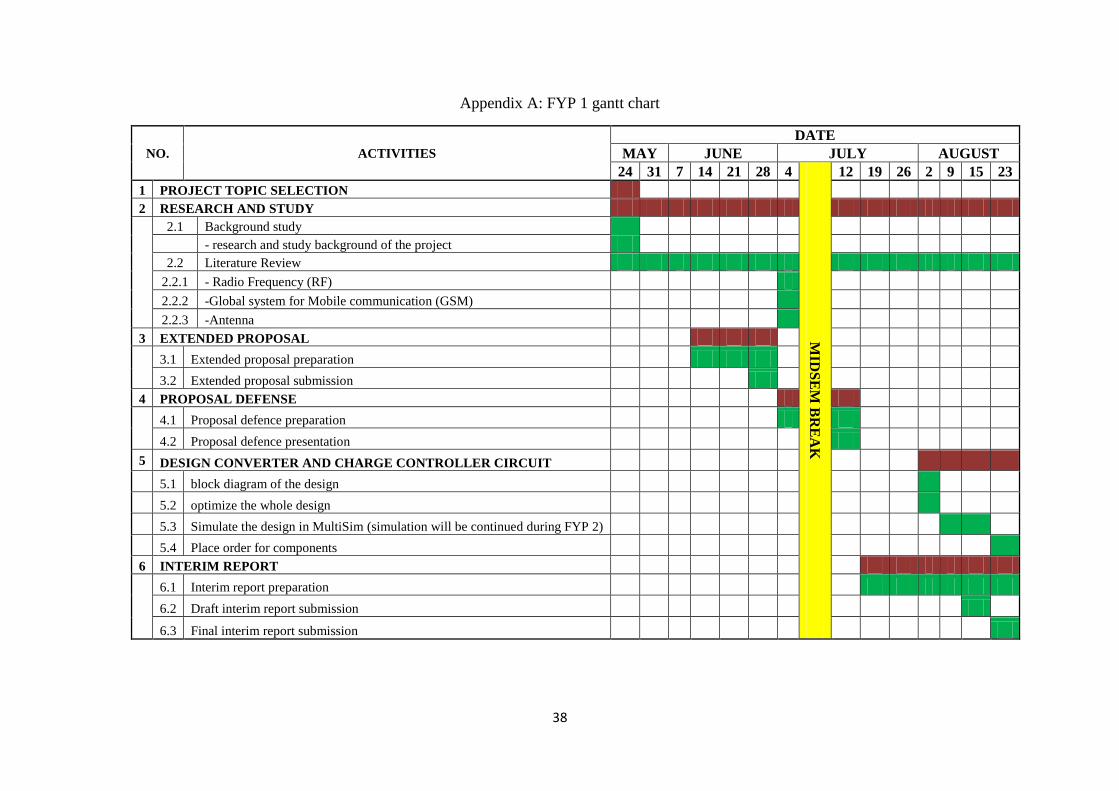
A FYP 1 Gantt Chart
B FYP 2 Gantt Chart
C Datasheet for OA 90 germanium diode
D Datasheet for LT 1763
38
Appendix A: FYP 1 gantt chart
NO. ACTIVITIES
DATE
MAY JUNE JULY AUGUST
24 31 7 14 21 28 4
MID
SE
M B
RE
AK
12 19 26 2 9 15 23
1 PROJECT TOPIC SELECTION
2 RESEARCH AND STUDY
2.1 Background study
- research and study background of the project
2.2 Literature Review
2.2.1 - Radio Frequency (RF)
2.2.2 -Global system for Mobile communication (GSM)
2.2.3 -Antenna
3 EXTENDED PROPOSAL
3.1 Extended proposal preparation
3.2 Extended proposal submission
4 PROPOSAL DEFENSE
4.1 Proposal defence preparation
4.2 Proposal defence presentation
5 DESIGN CONVERTER AND CHARGE CONTROLLER CIRCUIT
5.1 block diagram of the design
5.2 optimize the whole design
5.3 Simulate the design in MultiSim (simulation will be continued during FYP 2)
5.4 Place order for components
6 INTERIM REPORT
6.1 Interim report preparation
6.2 Draft interim report submission
6.3 Final interim report submission

39
Appendix B: FYP 2 gantt chart
NO. ACTIVITIES
DATE
SEP OCT NOV DEC JAN
27 4 11 18 25
MID
SE
M B
RE
AK
4 11 22 29 4 13 16 23 31 10
1 SIMULATION
1.1 Simulation in Multisim
1.2 analyze the output current and voltage
2 PROTOTYPE
2.1 circuit fabrication
2.1.1 voltage multiplier
2.1.2 current amplifier
2.2 testing on circuits
2.3 final prototyping
3 PROGRESS REPORT
3.1 Progress report preparation
3.2 Progress report submission
4 PRE- EDX
4.1 Pre- EDX preparation
4.2 Pre- EDX presentation
5 TECHNICAL REPORT
5.1 Technical report preparation
5.2 Technical report submission
6 FINAL REPORT
6.1 Final report preparation
6.2 draft final report submission
6.3 final report submission
6.4 final report (hard bound) submission
7 VIVA

40