energy& rsc events 2013 environmental...
TRANSCRIPT

ISSN 1754-5692
Energy&Environmental Sciencewww.rsc.org/ees Volume 6 | Number 3 | March 2013 | Pages 681–1048
REVIEW ARTICLECharles M. Lieber et al.Semiconductor nanowires: a platform for exploring limits and concepts for nano-enabled solar cells
Register with us and keep ahead in your field
RSC Events 2013Advancing knowledge in the chemical sciences
Major Scientific ConferencesFabrication, Structure and Reactivity of Anchored Nanoparticles (FD162)10-12 April 2013, Berlin, Germanyhttp://rsc.li/fd162
Photo-initiated Quantum Molecular Dynamics (FD163)15-17 April 2013, Nottingham, UKhttp://rsc.li/fd163
Challenges in Organic Materials & Supramolecular Chemistry (ISACS10)18-21 June 2013 , Kyoto, Japanhttp://rsc.li/isacs10
Electroanalysis at the Nanoscale (FD164)1-3 July 2013, Durham, UKhttp://rsc.li/fd164
Analytical Research Forum (ARF13)8-10 July 2013, Hertfordshire, UKhttp://rsc.li/arf13
11th International Conference on Materials Chemistry (MC11)8-11 July 2013, University of Warwick, UKhttp://rsc.li/mc11
Tropospheric Aerosol - Formation, Transformation, Fate and Impacts (FD165)22-24 July 2013, Leeds, UKhttp://rsc.li/fd165
23rd International Symposium: Synthesis in Organic Chemistry22-25 July 2013 , Oxford, UKhttp://rsc.li/os23
Challenges in Chemical Biology (ISACS11)23-26 July 2013, Boston, USAhttp://rsc.li/isacs11
Challenges in Chemical Renewable Energy (ISACS12)3-6 September 2013, Cambridge, UKhttp://rsc.li/isacs12
Advancing the Chemistry of the Actinides (DD14)16-18 September 2013, Edinburgh, UKhttp://rsc.li/dd14
Self-Assembly of Biopolymers (FD166)16-18 September 2013, Bristol, UKhttp://rsc.li/fd166
Mesostructure and Dynamics in Liquids and Solutions (FD167)18-20 September 2013, Bristol, UKhttp://rsc.li/fd167
http://rsc.li/eventsRegistered charity number 207890

Energy &Environmental Science
REVIEW
Semiconductor na
aDepartment of Chemistry and Chemical B
Massachusetts 02138, USA. E-mail: cml@cmbSchool of Engineering and Applied Sci
Massachusetts 02138, USAcDepartment of Physics, Korea University, Se
Cite this: Energy Environ. Sci., 2013, 6,719
Received 25th November 2012Accepted 16th January 2013
DOI: 10.1039/c3ee24182c
www.rsc.org/ees
This journal is ª The Royal Society of
nowires: a platform for exploringlimits and concepts for nano-enabled solar cells
Thomas J. Kempa,a Robert W. Day,a Sun-Kyung Kim,ac Hong-Gyu Parkc
and Charles M. Lieber*ab
Over the past decade extensive studies of single semiconductor nanowire and nanowire array photovoltaic
devices have explored the potential of these materials as platforms for a new generation of efficient and
cost-effective solar cells. This feature review discusses strategies for implementation of semiconductor
nanowires in solar energy applications, including advances in complex nanowire synthesis and
characterization, fundamental insights from characterization of devices, utilization and control of the
unique optical properties of nanowires, and new strategies for assembly and scaling of nanowires into
diverse arrays that serve as a new paradigm for advanced solar cells.
Broader context
The solar power received by the earth dwarfs global power demands by several orders-of-magnitude. Photovoltaics convert light to electrical energy and have thepotential to partially replace current energy technologies that rely on carbon-based fuels. At present, however, a lack of infrastructure and the high costs ofphotovoltaics prevent realizing this attractive goal. New ideas and materials are being explored to develop next-generation solar cells that could operate moreefficiently and be produced at lower cost. Nanowires have emerged as one promising platform to explore such new concepts. Their small dimensions allow forefficient charge separation and light absorption properties that are unique as compared to bulk materials. Furthermore, the synthesis and fabrication ofnanowire devices differs signicantly from traditional wafer-based technologies, thus presenting new opportunities such as use of less abundant materials orcheaper substrates. Here, we discuss the benets and remaining challenges of nanowires for photovoltaics and review progress towards understanding andoptimizing the electrical and optical performance of nanowire devices. We focus on single nanowire studies that can dene intrinsic limits for what is achievablewhen multiple nanowires are assembled. Challenges and initial progress towards scaling are presented, and, for the rst time, we articulate unique capabilitiesof solar cells derived from multiple, distinct nanowires.
1 Introduction
The energy received by the earth from the sun in one hourcould provide 80% of the energy that was consumed globally in2008 at an average rate of �17 TW.1 Photovoltaic (PV) solar cellsare the most common form of light to electrical powerconverter. For over two decades, single- and poly-crystallinesilicon solar cells have dominated the world market for PVswith recent average annual growth in capacity exceeding 70%.2
Nevertheless, installed PV capacity levels (40 GW in 2010)2
represent only �0.2% of total energy consumption, and remainlow largely due to a PV efficiency to cost metric that isuncompetitive3 with conventional power generation strategiessuch as fossil fuel or nuclear. Although there are lower costtechnologies based on thin lm solar cells such as CuInx-
Ga1�xSe2, CdTe, and amorphous silicon,4–7 these solar cellssacrice efficiency and have not reached grid parity.3
iology, Harvard University, Cambridge,
liris.harvard.edu
ences, Harvard University, Cambridge,
oul 136-701, Republic of Korea
Chemistry 2013
Fundamentally, the high cost of solar power3 is driven byexpensive feedstock (e.g. high purity Si), scarcity of feedstock(e.g. rare semiconductors), and expensive material processing/purication (e.g. high temperature or high vacuum syntheses),while low efficiencies result from incomplete light absorption,carrier recombination, and thermalization losses.8,9 Seeking tobreak this impasse, research in next-generation solar cells aimsto achieve greater than 20% solar to electric power conversionefficiencies at a specic cost of less than $0.50 per peak Watt.3
While conventional technologies have steadily improved anddecreased cost, there are ample opportunities to explore newmaterials and concepts that could lead toward high-efficiencyand low-cost solar cells.
2 Nanowires as a PV platform
The eld of nanoscience has provided scientists and engi-neers with a diverse set of materials including nano-particles,10–13 one-dimensional (1D)14–18 and 2D19,20 carbonmaterials, and metallic and semiconductor 1D nanowires21–25
(NWs). Over the past decade, several motivations have fueledintensive research in NWs and how these materials
Energy Environ. Sci., 2013, 6, 719–733 | 719
Energy & Environmental Science Review
could increase efficiency and reduce cost in solar cells. Oneproposed motivation is that bottom-up syntheses could yieldnew device architectures difficult or impossible to realize byconventional planar fabrication strategies. For example, it hasbeen shown that larger lattice mismatches can be accommo-dated during heteroepitaxial growth of nanoscale semi-conductor heterostructures.26,27,55 Second, it is possible toprepare NWs with lower thermal budgets and with less complexfabrication steps than typically required for top-down manu-facture of conventional solar cells.28�30 Third, the use of exibleand/or transparent substrates could reduce cost and expand theubiquity of solar cells in applications ranging from building-integrated to fabric-integrated PV. Fourth, the unique charac-teristics of light interaction with subwavelength NWs and
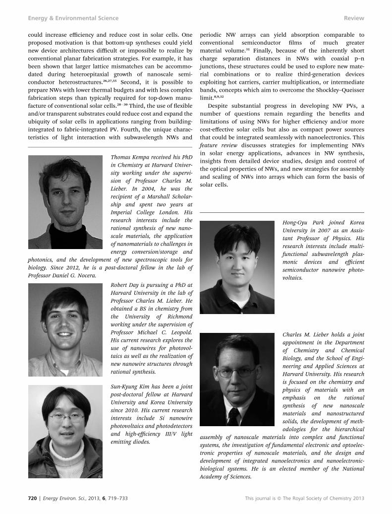
Thomas Kempa received his PhDin Chemistry at Harvard Univer-sity working under the supervi-sion of Professor Charles M.Lieber. In 2004, he was therecipient of a Marshall Scholar-ship and spent two years atImperial College London. Hisresearch interests include therational synthesis of new nano-scale materials, the applicationof nanomaterials to challenges inenergy conversion/storage and
photonics, and the development of new spectroscopic tools forbiology. Since 2012, he is a post-doctoral fellow in the lab ofProfessor Daniel G. Nocera.
Robert Day is pursuing a PhD atHarvard University in the lab ofProfessor Charles M. Lieber. Heobtained a BS in chemistry fromthe University of Richmondworking under the supervision ofProfessor Michael C. Leopold.His current research explores theuse of nanowires for photovol-taics as well as the realization ofnew nanowire structures throughrational synthesis.
Sun-Kyung Kim has been a jointpost-doctoral fellow at HarvardUniversity and Korea Universitysince 2010. His current researchinterests include Si nanowirephotovoltaics and photodetectorsand high-efficiency III/V lightemitting diodes.
720 | Energy Environ. Sci., 2013, 6, 719–733
periodic NW arrays can yield absorption comparable toconventional semiconductor lms of much greatermaterial volume.31 Finally, because of the inherently shortcharge separation distances in NWs with coaxial p–njunctions, these structures could be used to explore new mate-rial combinations or to realize third-generation devicesexploiting hot carriers, carrier multiplication, or intermediatebands, concepts which aim to overcome the Shockley–Queisserlimit.8,9,32
Despite substantial progress in developing NW PVs, anumber of questions remain regarding the benets andlimitations of using NWs for higher efficiency and/or morecost-effective solar cells but also as compact power sourcesthat could be integrated seamlessly with nanoelectronics. Thisfeature review discusses strategies for implementing NWsin solar energy applications, advances in NW synthesis,insights from detailed device studies, design and control ofthe optical properties of NWs, and new strategies for assemblyand scaling of NWs into arrays which can form the basis ofsolar cells.
Hong-Gyu Park joined KoreaUniversity in 2007 as an Assis-tant Professor of Physics. Hisresearch interests include multi-functional subwavelength plas-monic devices and efficientsemiconductor nanowire photo-voltaics.
Charles M. Lieber holds a jointappointment in the Departmentof Chemistry and ChemicalBiology, and the School of Engi-neering and Applied Sciences atHarvard University. His researchis focused on the chemistry andphysics of materials with anemphasis on the rationalsynthesis of new nanoscalematerials and nanostructuredsolids, the development of meth-odologies for the hierarchical
assembly of nanoscale materials into complex and functionalsystems, the investigation of fundamental electronic and optoelec-tronic properties of nanoscale materials, and the design anddevelopment of integrated nanoelectronics and nanoelectronic-biological systems. He is an elected member of the NationalAcademy of Sciences.
This journal is ª The Royal Society of Chemistry 2013

Review Energy & Environmental Science
3 Strategies for implementation ofnanowire solar cells
One strategy for NW solar cells relies on synthesis of NWbuilding blocks and the subsequent assembly of these intocomplex multi-component devices (Fig. 1). In this paradigm,sophisticated NW building blocks are synthetically encodedwith distinct electrical and optical properties and then tested onthe level of single devices. Results from single NW devicecharacterization can subsequently provide feedback for thedesign of new functional NWs. Finally, NWs can be assembledto form highly differentiated structures that have propertiesdistinct frommonolithic or top-down processed semiconductorarchitectures.
To illustrate the logic of this paradigm, we propose a uniqueNW-enabled solar cell: the assembled NW ‘multi-junction’ solarcell. In an example of our concept (Fig. 1C), 3 distinct NWs aresynthesized to absorb efficiently blue, green, and red light. Bystacking and interconnecting these horizontally oriented NWsin the appropriate vertical order, one can realize a multi-junc-tion solar cell with efficient absorption of solar spectrum, whilesimultaneously eliminating many of the signicant challengesand costs associated with traditional multi-junction thin-lmsolar cells, such as epitaxial growth or wafer-bonding of III/Vmaterials.33,55
This bottom-up approach41,42 has been used previously torealize numerous nanoscale functional devices,34–40 and also hasadvantages43 for the development of next-generation solar cells:(1) synthesis can encode functionality in the form of chemical(e.g. doping) and structural (e.g. interfaces, grain boundaries,morphologies) compositions which can be tuned from themicro-, nano-, to atomic length-scales; and (2) assembly cancombine diverse NW materials and structures on varioussubstrates (e.g. glass, foil, plastic) to build a complex multi-component system with properties distinct from the individualbuilding blocks.
Simultaneously, numerous groups have investigated analternative strategy based on growth of large-area NW or
Fig. 1 Bottom-up design of NW based solar cells. (A) Schematic of coaxial NWbuilding blocks (blue indicates p-type doped core and beige indicates n-typedoped shells). (B) Schematic of typical silicon core/shell NW device fabricatedfrom one NW building block from (A) on arbitrary substrate with integrated back-side reflector. (C) Schematic illustrating potential for new device architectureusing distinct NW building blocks within each layer. Colors indicate peak wave-length of light absorbed for particular NW morphology.
This journal is ª The Royal Society of Chemistry 2013
microwire arrays wherein the wires are oriented with their longaxis perpendicular to the substrate and where the deviceconguration is xed during subsequent device fabrication.44
Such an approach can deliver several benets including: (1)device fabrication which is potentially scalable to large-areadevices/modules; and (2) enhanced absorption due to longoptical path-lengths and photonic effects which can persist inperiodic vertically oriented NW arrays.45,46 As an example,research groups investigating arrays of Si microwires havedemonstrated light scattering/trapping effects from periodicand random arrangement of high-refractive index semi-conductor microwire arrays.45 As another example, a ZnO NWphotoanode was utilized to enhance the current density in adye-sensitized solar cell due to increased loading of Ru-dye ontoZnO NW surfaces and improved charge percolation.47 There arealso challenges associated with this vertical NW array approach,including formation of good electrical contacts to both sides ofthe PV junction and uncertain cost competitiveness relative totraditional technologies stemming primarily from reliance onpreparation of NW arrays from crystalline wafers. Detaileddiscussion of vertically oriented arrays is beyond the scope ofthis review but has been recently reviewed.31,93
4 Nanowire synthesis, characterization andcontrol
Nanowire PV devices can incorporate p-type/intrinsic/n-type (p–i–n) dopant modulation for carrier separation in 2 distinctmotifs: (1) axial geometry with junction encoded along thegrowth direction of the NW, and (2) radial geometry withjunction encoded between the core and coaxial shells. Sche-matics of a single p–i–n axial and radial nanowire diode areshown in Fig. 2, where pink, yellow, and blue regions denote p-type, intrinsic, and n-type diode segments, respectively. In thesestructures, electron–hole pairs are generated upon absorptionof photons whose energies are equal to or greater than the band-gap of silicon (Eg ¼ 1.12 eV for single-crystal silicon). Carriergeneration and separation are most efficient within the deple-tion region due to the built-in eld established across the p–i–njunction.34–36,48 Photogenerated holes (electrons) dri in thepresence of the electric eld through the p-type (n-type) regionsand are ultimately collected as photocurrent by ohmic metal
Fig. 2 Axial and radial structures form basis of NW PV. Top: coaxial NW withcarrier separation occurring in the radial direction. Bottom: axial NW with carrierseparation occurring along the axial direction. Pink indicates p-type doping,yellow indicates intrinsic (undoped), and blue indicates n-type doping.
Energy Environ. Sci., 2013, 6, 719–733 | 721

Energy & Environmental Science Review
contacts. In the axial conguration, the p-type and n-typeregions can be made arbitrarily short since their main purposeis to provide contact to the junction encoded within the nano-wire. One attractive consequence of this is that the active devicearea can be kept small so as to enhance integration with othernanodevices or nanoelectronic circuits. In the radial congu-ration, the p–i–n interface extends along the length of thenanowire allowing carrier separation to take place in the radialversus the longer axial direction. In this structure, carriercollection distances are smaller or comparable to the minoritycarrier diffusion length4,46 meaning that photogeneratedcarriers can reach the p–i–n junction with high efficiencywithout substantial bulk recombination, even in poor-quality orlow-mobility materials.
Fig. 3 Introduction to synthesis examples of techniques. (A–F) Schematics forVLS core growth (A, C and E) using metal catalyst at lower temperature, and shellgrowth (B, D and F) at higher temperatures. (G) SEM image of facetted Si core/shell p/in NW synthesized by CVD; scale bar 150 nm. (H) TEM image of solution-processed core/shell CdS/Cu2S NW. (I) SEM images of InAs NWs exhibiting peri-odic coherent twin superlattice structures and their associated three-dimensionalatomic model. Panels A–F reproduced with permission from ref. 91 ª The RoyalSociety. Panels H and I reproduced with permission from ref. 52 and 53 ª Mac-millan Publishers Limited.
4.1 Synthesis of nanowires
Semiconductor NWs are typically synthesized using the nowwell-established metal nanocluster-catalyzed vapour–liquid–solid (VLS) growth process.21,22,41,49 In this process (Fig. 3A), avapour-phase semiconductor source dissolves in the liquidmetal/semiconductor droplet maintained at a temperature nearor above the metal/semiconductor eutectic point. Continuedsupply of the gaseous source supersaturates the droplet and thechemical potential between the gas–liquid and liquid–solidinterfaces acts as a driving force for nucleation of the solidsemiconductor. During growth, the liquid–solid interface is thesite for continued incorporation of crystalline solid materialinto the elongating NW.
Axial NWs are obtained through VLS growth as illustrated inFig. 3C and E. Growth of NW axial heterostructures entails useof various reactant sources (e.g. dopant or other semiconductorprecursors) and it is therefore important to select a nanoclustercatalyst that can maintain a stable eutectic under compatibleconditions. Radial or core/shell heterostructures are obtainedby shiing growth conditions from VLS to a vapour–solidgrowth regime where dissociation and deposition of reactants ispromoted on the NW surface (Fig. 3B) resulting in concentricshells.27 Radial NWs encode function in the form of coaxialshells (Fig. 3D and F) and afford several advantages ascompared to VLS-grown axial NWs, including: (1) orthogonali-zation of carrier separation and collection into radial and axialcomponents, (2) atomically sharp interfaces are accessible dueto the layer-by-layer vapour-phase growth mechanism, and (3)greater freedom to synthesize new structures because of thebroad range of parameters for shell growth, which will be dis-cussed below.
A diversity of solution-phase and gas-phase techniques existsfor the synthesis of semiconductor NWs. Chemical vapordeposition (CVD) has been broadly adopted for growth of groupIV, III/V, and II/VI semiconductor NWs and, in a few instances,molecular beam epitaxy (MBE) from gas50 and solid-stateprecursors has also been utilized. Metal–organic chemicalvapour deposition (MOCVD)51 has been extensively applied forgrowth of compound semiconductor NWs.54–56 Silicon core/multi-shell NWs with high-quality electronic interfaces wererecently synthesized using a low-pressure CVD method tailored
722 | Energy Environ. Sci., 2013, 6, 719–733
to elicit a polymorphic crystal structure with very low defectdensities.34 A scanning electron microscopy (SEM) image ofsuch a Si NW (Fig. 3G) reveals smooth facet surfaces distinctfrom the disordered and un-faceted nanocrystalline morphol-ogies previously reported.36 In this work, the high-quality NWmaterial led to the rst demonstration of Si NW solar cells withlarge VOC's of 0.5 V. In addition, low-temperature, solution-phase doping of CdS NWs with Cu (Fig. 3H) has been used toform active devices with good electrical properties, includingVOC's of ¼ 0.6 V and efficiencies of 5.4%.52 In addition, theSamuelson group has pioneered the use of molecular organicvapour phase epitaxy (MOVPE) to grow III/V NWs. In a recentwork, the Samuelson group demonstrated the ability to selec-tively incorporate polytypic and twin-plane superlattices in InAs
This journal is ª The Royal Society of Chemistry 2013

Review Energy & Environmental Science
NWs (Fig. 3I) and showed how these crystallographic manipu-lations can be tuned with well-dened synthetic parametersincluding temperature and diameter.53 Together, these reportsunderscore the range of synthetic systems available for growthof semiconductor NWs.
4.2 Nanowires: diversity in material, structure, andmorphology
Synthetic advances in the growth of group IV, III/V, and II/VIsemiconductor NWs have correspondingly enabled substantialprogress in transistor, laser, and solar-cell devices. For example,Ge/Si core/shell nanowires were rst prepared by nanocluster-catalyzed VLS-growth of crystalline Ge cores followed by low-temperature deposition of an a-Si shell that was subsequentlyannealed.27 The resulting high-resolution transmission electronmicroscopy (TEM) images and energy dispersive X-ray spec-troscopy (EDS) maps of Si and Ge (Fig. 4A) conrmed that thenanowire heterostructures possessed abrupt and crystallineinterfaces. MOCVD synthesis of defect-free InGaN/GaN NWswith 26 multiple quantum well (MQW) structures54 (Fig. 4B andC) further demonstrated the potential for implementingcomplex structures at the nanoscale using materials whoselarge lattice mismatches could not be easily accommodated inthin lms.57 Finally, it has been demonstrated recently that axialNWs can be induced to kink at specic points through transient
Fig. 4 Material and structural diversity. (A) Bright-field TEM images of Ge/Si core/simage of the cross-section of an InGaN/GaN multiple quantum well NW; scale barerointerfaces; scale bar 10 nm. (D) SEM image of a multiply kinked CdS NW grown by27, 54 and 58 ª Macmillan Publishers Limited.
This journal is ª The Royal Society of Chemistry 2013
modulation of growth pressure and that multiple kinks can beencoded through iterative application of such modulations.58 Inaddition to Si and Ge kinked NWs, group II/VI multiply kinkedCdS NWs were synthesized (Fig. 4D), thus demonstrating thegenerality of this approach.
In addition to the many semiconductor materials andstructural types accessible via controlled synthesis, uniquemorphologies are possible through tailored synthesis of Si NWs.It is possible to synthesize NWs with hexagonal, octagonal, andrectangular cross-sections (Fig. 5A) through modication of theaforementioned core/shell synthesis (e.g. shell growth temper-ature, silane partial pressure, etc.). Specically, bright-eld TEMimages of Si core/multi-shell NWs sectioned ca. perpendicularto their axes reveal a hexagonal cross-section34 with well-denedsurface facets (Fig. 5B). By growing the nal, n-type doped, shellof this NW at 860 �C instead of the typical 775 �C, Si depositioncan be accelerated on the {113} facets59 leading to a NW with anapproximately rectangular cross-section (Fig. 5B). Control ofmorphology is also possible through subtle modulations incrystal structure within the cross-section of a NW. A dark-eldTEM image (Fig. 5C) of the hexagonal Si cross-section shown inFig. 5B reveals more detail regarding the internal crystal struc-ture of the NW. A thin polycrystalline region surrounding the100 nm NW core is visible as brighter contrast, as are otherdistinct features such as grain boundaries. Although structuralheterogeneity exists in the NW, its electron diffraction pattern
hell NW with EDS mapping of Ge (red) and Si (blue) elements. (B) Dark-field TEM, 100 nm. (C) Bright-field TEM image of an InGaN/GaN structure illustrating het-VLS mechanism; scale bar, 1 mm. Panels A–D reproduced with permission from ref.
Energy Environ. Sci., 2013, 6, 719–733 | 723

Fig. 5 Si NW PV: Characterization and control over morphology. (A) SEM imagesof various core/shell NW building blocks enabled by rational control of synthesis.(B) Bright-field TEM images of cross-sections of hexagonal and rectangular core/shell NWs; scale bars, 50 nm. (C) Dark-field image of the cross-section of a core/multi-shell Si NW showing distinct crystallographic interfaces and its accompa-nying electron diffraction pattern along the [112] direction. Panel B left and panelC right reproduced with permission from ref. 34 ª National Academy of Sciencesof the United States of America. Panel B right reproduced with permission fromref. 59 ª American Chemical Society.
Fig. 6 Si NW PV: Control of interfaces and doping. (A) Left: schematic of dopingand morphology of p/pin core/shell NW. Right: high resolution, aberration cor-rected TEM image of Si shell from area indicated in purple box of schematic. Blueindicates n-type doping, white indicates intrinsic (undoped), and red indicates p-type doping. (B) EDSmapping of phosphorus atoms within Si core/shell p/pin NWacquired on STEM. Panel B reproduced with permission from ref. 34 ª NationalAcademy of Sciences of the United States of America.
Energy & Environmental Science Review
(Fig. 5C) is consistent with reections from the diamond cubiclattice of Si oriented along h211i, from which we conclude thatthe individual crystal domains share the same orientation asthe core. Interestingly, variations in internal crystal morphologyand cross-sectional morphology can have signicant effects onlight absorption in these subwavelength cavities. These featuresand their implications for NW PV devices will be discussed indetail below.
724 | Energy Environ. Sci., 2013, 6, 719–733
The realization of well-dened nanoscale interfaces forcharge separation is vital to the electrical performance of NWsolar cells. Representative high-resolution TEM images of cross-sections of core/multi-shell Si NWs (Fig. 6A) show clear (111)lattice fringes continuing up to the amorphous SiO2 coating atthe outermost edge of the NW.34 These data reveal that over anarea of the cross-section spanning the width of the p–i–njunction there are minimal crystal defects. Low defect densitiesare an important criterion for high-quality electrical interfacesin photodetector, photonic, or solar cell applications. In addi-tion, EDS mapping data were used to characterize the phos-phorous dopant and oxygen proles in a Si core/shell cross-sectional sample (Fig. 6B). The phosphorous prole exhibits twopeaks coincident with the le and right sides of the outer n-shell which have peak widths, 20–30 nm, in good agreementwith the expected n-shell thickness of 25 nm based onmeasured growth rates.34 Such measurements verify that well-dened, nanoscale dopant variations can be encoded in core/shell NWs and, more generally, demonstrate the controlpossible with bottom-up synthesis.
5 Device electrical transport andperformance
Fundamental studies of NWs for next-generation solar cellsinvolves two important steps: (1) synthesis of NW componentswith precisely dened structural and chemical properties, and(2) elucidation of PV properties at the single NW level, whichpermits determination of the optoelectronic properties,intrinsic limits, and potential benets of NWs for solar cells.
For device fabrication, NWs must be transferred from theirgrowth substrates to a host substrate that will support the NW
This journal is ª The Royal Society of Chemistry 2013
Review Energy & Environmental Science
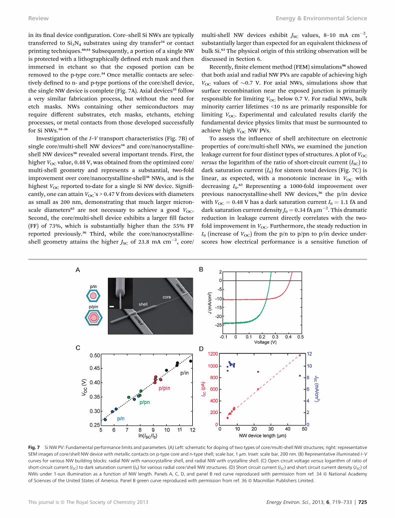
in its nal device conguration. Core–shell Si NWs are typicallytransferred to Si3N4 substrates using dry transfer34 or contactprinting techniques.60,61 Subsequently, a portion of a single NWis protected with a lithographically dened etch mask and thenimmersed in etchant so that the exposed portion can beremoved to the p-type core.34 Once metallic contacts are selec-tively dened to n- and p-type portions of the core/shell device,the single NW device is complete (Fig. 7A). Axial devices35 followa very similar fabrication process, but without the need foretch masks. NWs containing other semiconductors mayrequire different substrates, etch masks, etchants, etchingprocesses, or metal contacts from those developed successfullyfor Si NWs.34–36
Investigation of the I–V transport characteristics (Fig. 7B) ofsingle core/multi-shell NW devices34 and core/nanocrystalline-shell NW devices36 revealed several important trends. First, thehigher VOC value, 0.48 V, was obtained from the optimized core/multi-shell geometry and represents a substantial, two-foldimprovement over core/nanocrystalline-shell36 NWs, and is thehighest VOC reported to-date for a single Si NW device. Signi-cantly, one can attain VOC's > 0.47 V from devices with diametersas small as 200 nm, demonstrating that much larger micron-scale diameters62 are not necessary to achieve a good VOC.Second, the core/multi-shell device exhibits a larger ll factor(FF) of 73%, which is substantially higher than the 55% FFreported previously.36 Third, while the core/nanocrystalline-shell geometry attains the higher JSC of 23.8 mA cm�2, core/
Fig. 7 Si NW PV: Fundamental performance limits and parameters. (A) Left: schemaSEM images of core/shell NW device with metallic contacts on p-type core and n-typcurves for various NW building blocks: radial NW with nanocrystalline shell, and radshort-circuit current (ISC) to dark saturation current (I0) for various radial core/shell NNWs under 1-sun illumination as a function of NW length. Panels A, C, D, and paof Sciences of the United States of America. Panel B green curve reproduced with p
This journal is ª The Royal Society of Chemistry 2013
multi-shell NW devices exhibit JSC values, 8–10 mA cm�2,substantially larger than expected for an equivalent thickness ofbulk Si.63 The physical origin of this striking observation will bediscussed in Section 6.
Recently, nite element method (FEM) simulations96 showedthat both axial and radial NW PVs are capable of achieving highVOC values of �0.7 V. For axial NWs, simulations show thatsurface recombination near the exposed junction is primarilyresponsible for limiting VOC below 0.7 V. For radial NWs, bulkminority carrier lifetimes <10 ns are primarily responsible forlimiting VOC. Experimental and calculated results clarify thefundamental device physics limits that must be surmounted toachieve high VOC NW PVs.
To assess the inuence of shell architecture on electronicproperties of core/multi-shell NWs, we examined the junctionleakage current for four distinct types of structures. A plot of VOCversus the logarithm of the ratio of short-circuit current (ISC) todark saturation current (I0) for sixteen total devices (Fig. 7C) islinear, as expected, with a monotonic increase in VOC withdecreasing I0.63 Representing a 1000-fold improvement overprevious nanocrystalline-shell NW devices,36 the p/in devicewith VOC ¼ 0.48 V has a dark saturation current I0 ¼ 1.1 fA anddark saturation current density J0¼ 0.34 fA mm�2. This dramaticreduction in leakage current directly correlates with the two-fold improvement in VOC. Furthermore, the steady reduction inI0 (increase of VOC) from the p/n to p/pn to p/in device under-scores how electrical performance is a sensitive function of
tic for doping of two types of core/multi-shell NW structures; right: representativee shell; scale bar, 1 mm. Inset: scale bar, 200 nm. (B) Representative illuminated I–Vial NW with crystalline shell. (C) Open circuit voltage versus logarithm of ratio ofW structures. (D) Short circuit current (ISC) and short circuit current density (JSC) ofnel B red curve reproduced with permission from ref. 34 ª National Academyermission from ref. 36 ª Macmillan Publishers Limited.
Energy Environ. Sci., 2013, 6, 719–733 | 725

Energy & Environmental Science Review
synthetically encoded junction properties. Notably, thetemperature coefficient of VOC extracted from I/V data acquireddown to 60 K is �1.9 mV K�1 and close to the value dVOC/dT ¼�1.7 mV K�1 calculated for bulk single-crystalline Si solarcells,64 which attests to the good transport characteristics ofcore/multi-shell NW devices. Interestingly, data obtained oncore/multi-shell NW devices with lengths spanning over 1 orderof magnitude (Fig. 7D) exhibit linear scaling of ISC and nearlyconstant JSC. This result conrms that NW device performanceis preserved over a large range of NW lengths and encouragesuse of these building blocks in future large-area arrays whichcould be fabricated solely by standard photolithography.Together, these data demonstrate that precise synthetic controlof NW structures is a powerful determinant of improvements inVOC, FF, and I0.
Several groups have proposed that metal nanocluster cata-lysts, especially gold, used in NW growth could enhancerecombination and adversely affect VOC in NW devices.65 Tofurther investigate this possibility, NWs were synthesized usingAl catalyst65 which, unlike Au, does not act as a mid-band gaptrap state in Si.66 Nevertheless, the best illuminated I–V curve forthe core/multi-shell diode geometry (Fig. 8A, grey curve) yields aVOC, 0.23 V, �2 times smaller than the value for analogous Au-catalyzed devices. Furthermore, even devices where Au wasremoved by wet-chemical etching of as-grown NW cores (Fig. 8,red curve) yielded a VOC, 0.44 V, similar to the best resultsobtained on core/multi-shell devices prepared without removalof the catalyst. Together, these results suggest that proposed Auimpurities do not signicantly lower VOC and again affirm thatthe overall quality of the core/multi-shell structure, as dictatedby synthesis, is the most important driver of good electricalperformance.
Fig. 8 Role of metal catalyst on PV performance. Left: illuminated I–V curves forSi core/shell p/i/n devices. Red curve corresponds to device from NW where Auwas etched prior to shell deposition. Grey curve corresponds to device from NWgrown with an Al catalyst. Bottom: SEM images of Au-etched and Al-catalyzedNWs; scale bar, 2 mm and 1 mm. Reproduced with permission from ref. 34 ªNational Academy of Sciences of the United States of America.
726 | Energy Environ. Sci., 2013, 6, 719–733
Several reports have also focused on the role of NW surfacestates in recombination of charge carriers. Using near-eldscanning optical microscopy (NSOM) to locally excite chargecarriers in a reverse-biased axial NW device, researchers foundthat a 10 nm a-Si shell can serve as effective passivation with a100-fold reduction in surface recombination.67 Furthermore,Kelzenberg et al. have performed scanning photocurrentmapping experiments on single Si microwire devices with p–njunctions and diameters between 1.2 and 1.8 mm. They discov-ered that while a thin a-Si:H passivation layer can provide asurface recombination velocity of S � 450 cm s�1, a-SiNx:Hprovides superior passivation with S � 70 cm s�1 and a corre-spondingly very long minority-carrier diffusion length Ln [
30 mm.62 Together, these results argue that with proper passiv-ation it is possible to improve the electrical performance ofNW devices.
6 Light absorption in nanowires
In addition to good electrical performance, a solar cell mustabsorb signicant light in order to achieve high efficiency.Conventional semiconductor devices, such as bulk crystallineor thin-lm solar cells, achieve greater light absorption by use ofthicker absorbing layers68 and/or anti-reection techniques (e.g.surface texturing69–71 or a quarter-wave dielectric coating72,73).However, increased material usage and additional fabricationsteps typically increase cost.74 Absorption of light by NWs issignicantly distinct from bulk material absorption. Severalgroups have shown that subwavelength size, high-refractiveindex NWs can absorb a signicant amount of light using afraction of the volume needed with bulk semiconductormaterial.34,59,75
To develop more efficient NW PV devices, signicant efforthas focused on how the absorption properties of NWs depend onmaterial, size, and cross-sectional morphology.34,59,75–77 Syntheticcontrol over these parameters may allow the design of NWdevices with absorption characteristics distinct from traditionalcrystalline wafer or thin-lm structures.34,59 In addition to lightabsorption at the single NW level, horizontally75,78 or verticallyoriented45,79NWarrays with appropriately chosen pitch size havebeen shown to exhibit broadband anti-reection as well asenhanced light-scattering. The following sections discuss theorigin of distinct light absorption, and strategies to tune lightabsorption in single NWs and their assembled structures. Weemphasize that synthesis affords a high degree of control to tuneand optimize light absorption in these materials for PV.
6.1 Introduction and basic theory
Semiconductor NWs are subwavelength optical cavities that cansupport resonant modes. To exploit the optical properties ofNWs it is necessary to quantify their optical resonances throughcalculation34,59,75–77,80,81 and measurement.34,59,75–77,82 Simulationsillustrate how a NW interacts with incident light and candescribe in detail the properties (e.g. prole and amplitude) ofresonant modes. Measurements, typically photocurrent spectraof single NW devices, provide crucial verication of simulation
This journal is ª The Royal Society of Chemistry 2013

Review Energy & Environmental Science
and combined with calculations allow for design of new NW-based optical cavities.
Analytical Lorentz–Mie theory75,76,80,81 or numerical full-eldelectromagnetic simulations34,59,77 have been widely used forstudying light–matter interaction in nanowires. For example, innite-difference time-domain (FDTD) simulations, a normallyincident plane wave with a specic wavelength and polarizationstate (i.e. transverse-electric (TE) or transverse-magnetic (TM))interacts with a NW cavity, as shown in Fig. 9A. The calculatedelectric eld distribution illustrates that a Si NW can, at specicwavelengths, absorb incident photons beyond its physical cross-section; this phenomenon is called the ‘optical antennaeffect’.34,75,77,83,84 The absorption mode prole at a specicwavelength (Fig. 9B) can be obtained by recording J$E at eachgrid point within a NW, where J and E are the polarizationcurrent density and electric eld, respectively. The NW cavitymodes have localized spatial proles, including Fabry–Perot,whispering gallery, and higher-order complex modes at partic-ular wavelengths. A combination of optical antenna effects anddistinct resonant modes in NWs leads to light absorption thatdiffers signicantly from bulk material absorption.
Experiments to verify and quantify simulated optical prop-erties of NWs have been carried out by measuring photocurrentspectra of single NW PV devices34,59,62 or photodiodes.75�77,85 Forexample, external quantum efficiency (EQE) values of �0.15have been reported for micro-wire devices based on Al–SiSchottky junctions.85 Relative EQE values have been alsoreported for Si75,77 and Ge76 nanowire devices acting as photo-detectors. Signicantly, measurement of the absolute EQE from
Fig. 9 Optical resonant modes in NWs and measurement of absolute EQE. (A) Eleccavity. (B) Various absorption mode profiles corresponding to different peaks in EQEmode. (C) Experimental (black) and simulated (red) EQE spectrum of core/shell hexthickness of bulk Si plotted in green for comparison. (D) Relative absorption efficiencypermission from ref. 59 ª American Chemical Society. Panels B and C reproduced wiAmerica. Panel D reproduced with permission from ref. 92 ª Macmillan Publishers
This journal is ª The Royal Society of Chemistry 2013
Si NW PV devices has been reported in several instances.34,59
Shown in Fig. 9C is a representative result of the absolute EQEversus wavelength acquired for a p–i–n core/multi-shell NWdevice and a simulated spectrum of the same structure. Boththe experimental and simulated spectra are highly structured,with good agreement in the peak wavelengths and amplitudes,where the only adjustable parameter in the FDTD simulationwas the size of the NW. By comparing the experimental andsimulated spectra, peaks in the experimental spectrum areassigned to specic resonant absorption modes (Fig. 9B).Finally, the EQE spectrum approaches and even exceeds unityfor wavelengths in the range of 400–500 nm which is a mani-festation of the optical antenna effect.34,62,83 This effect is purelyclassical and caused by the sub-wavelength diameter of the NW.To calculate EQE from photocurrent or from simulatedabsorption data, the projected area of the NW (normal tosubstrate plane) was used. EQE values greater than unity can beobtained because the absorption cross-section of a single NWcan exceed its physical cross-section for some photon energies.Fig. 9D presents the normalized absorption spectra for Ge NWphotodetectors with diameters ranging from 10 to 110 nm.92
Taken together, these ndings demonstrate that semiconductorNWs can sustain distinct wavelength-dependent absorptioncharacteristics across a large range of the solar spectrum.
6.2 Size and morphology effects
One attractive feature of subwavelength size cavities is that nechanges to their structure can lead to dramatic alteration of
tric field intensity distribution illustrating vertically incident light coupling into NWspectrum. Arrow indicates relative wavelength of light needed to excite resonantagonal NW device with height ¼ 240 nm. Simulated EQE spectrum of equivalentfor Ge photodetector devices as function of wavelength. Panel A reproduced withth permission from ref. 34 ª National Academy of Sciences of the United States ofLimited.
Energy Environ. Sci., 2013, 6, 719–733 | 727
Energy & Environmental Science Review
their optical properties.86–88 Recent studies have revealed howmorphological changes (i.e. size and cross-sectionalmorphology) in NWs inuence their absorption characteris-tics.34,59,75–77 In general, the ability to signicantly tailorabsorption in NWs as compared to conventional planar struc-tures could drive development of efficient photovoltaic devicesas well as other photonic applications.
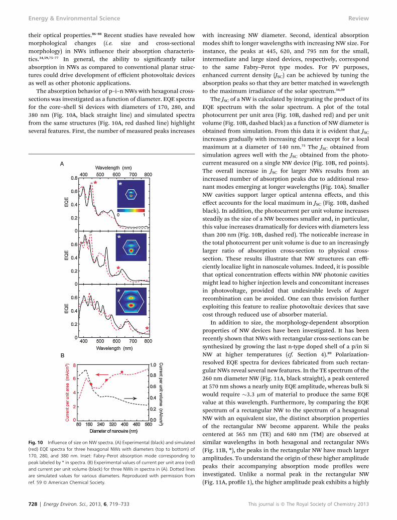
The absorption behavior of p–i–n NWs with hexagonal cross-sections was investigated as a function of diameter. EQE spectrafor the core–shell Si devices with diameters of 170, 280, and380 nm (Fig. 10A, black straight line) and simulated spectrafrom the same structures (Fig. 10A, red dashed line) highlightseveral features. First, the number of measured peaks increases
Fig. 10 Influence of size on NW spectra. (A) Experimental (black) and simulated(red) EQE spectra for three hexagonal NWs with diameters (top to bottom) of170, 280, and 380 nm. Inset: Fabry–Perot absorption mode corresponding topeak labeled by * in spectra. (B) Experimental values of current per unit area (red)and current per unit volume (black) for three NWs in spectra in (A). Dotted linesare simulated values for various diameters. Reproduced with permission fromref. 59 ª American Chemical Society.
728 | Energy Environ. Sci., 2013, 6, 719–733
with increasing NW diameter. Second, identical absorptionmodes shi to longer wavelengths with increasing NW size. Forinstance, the peaks at 445, 620, and 795 nm for the small,intermediate and large sized devices, respectively, correspondto the same Fabry–Perot type modes. For PV purposes,enhanced current density (JSC) can be achieved by tuning theabsorption peaks so that they are better matched in wavelengthto the maximum irradiance of the solar spectrum.34,59
The JSC of a NW is calculated by integrating the product of itsEQE spectrum with the solar spectrum. A plot of the totalphotocurrent per unit area (Fig. 10B, dashed red) and per unitvolume (Fig. 10B, dashed black) as a function of NW diameter isobtained from simulation. From this data it is evident that JSCincreases gradually with increasing diameter except for a localmaximum at a diameter of 140 nm.75 The JSC obtained fromsimulation agrees well with the JSC obtained from the photo-current measured on a single NW device (Fig. 10B, red points).The overall increase in JSC for larger NWs results from anincreased number of absorption peaks due to additional reso-nant modes emerging at longer wavelengths (Fig. 10A). SmallerNW cavities support larger optical antenna effects, and thiseffect accounts for the local maximum in JSC (Fig. 10B, dashedblack). In addition, the photocurrent per unit volume increasessteadily as the size of a NW becomes smaller and, in particular,this value increases dramatically for devices with diameters lessthan 200 nm (Fig. 10B, dashed red). The noticeable increase inthe total photocurrent per unit volume is due to an increasinglylarger ratio of absorption cross-section to physical cross-section. These results illustrate that NW structures can effi-ciently localize light in nanoscale volumes. Indeed, it is possiblethat optical concentration effects within NW photonic cavitiesmight lead to higher injection levels and concomitant increasesin photovoltage, provided that undesirable levels of Augerrecombination can be avoided. One can thus envision furtherexploiting this feature to realize photovoltaic devices that savecost through reduced use of absorber material.
In addition to size, the morphology-dependent absorptionproperties of NW devices have been investigated. It has beenrecently shown that NWs with rectangular cross-sections can besynthesized by growing the last n-type doped shell of a p/in SiNW at higher temperatures (cf. Section 4).89 Polarization-resolved EQE spectra for devices fabricated from such rectan-gular NWs reveal several new features. In the TE spectrum of the260 nm diameter NW (Fig. 11A, black straight), a peak centeredat 570 nm shows a nearly unity EQE amplitude, whereas bulk Siwould require �3.3 mm of material to produce the same EQEvalue at this wavelength. Furthermore, by comparing the EQEspectrum of a rectangular NW to the spectrum of a hexagonalNW with an equivalent size, the distinct absorption propertiesof the rectangular NW become apparent. While the peakscentered at 565 nm (TE) and 680 nm (TM) are observed atsimilar wavelengths in both hexagonal and rectangular NWs(Fig. 11B, *), the peaks in the rectangular NW have much largeramplitudes. To understand the origin of these higher amplitudepeaks their accompanying absorption mode proles wereinvestigated. Unlike a normal peak in the rectangular NW(Fig. 11A, prole 1), the higher amplitude peak exhibits a highly
This journal is ª The Royal Society of Chemistry 2013

Fig. 11 Influence of nanowire morphology on absorption. (A) Tranverse-electric EQE spectrum of rectangular morphology crystalline-Si NW device. Right: absorptionmode profiles corresponding to numbered peaks in spectrum. (B) Comparison of hexagonal versus rectangular EQE spectrum of unpolarized light. Data are from FDTDsimulations which assume equivalent height and diameters for both morphologies. (C) Simulated JSC values as a function of NW size for various morphologies ofamorphous silicon NWs. (D) Simulated absorption spectra for morphologies in (C). (E) Electric field intensity distribution for a particular resonant mode excited in thevarious morphologies shown in (C). Panels A and B reproduced with permission from ref. 59ª American Chemical Society. Panels C–E reproduced with permission fromref. 75 ª American Chemical Society.
Review Energy & Environmental Science
symmetric mode prole (Fig. 11A, prole 2). Since the lattermode matches with the cross-sectional morphology of therectangular NW it experiences lower optical loss.90 In conclu-sion, design of cross-sectional morphology can provide afeasible method to enhance absorption efficiency at specicwavelengths.
Recently, the morphology-dependent absorption propertiesof NWs with various cross-sections (i.e. square, circular,hexagonal, and triangular) were explored by performing full-eld electromagnetic simulations, as shown in Fig. 11C–E.75 Inthis simulation, amorphous Si NWs were considered. Theresults uncovered several trends that depend on the cross-section of a NW, including a wavelength shi of peaks between650 and 800 nm and a variation of JSC. However, this simulationdoes not reproduce the pronounced peaks at longer wave-lengths for a NW with rectangular cross-section as discussed inthe preceding paragraph. The discrepancy between these tworeported results lies in the absorber material: crystalline Si isinherently less absorptive than amorphous Si. For moreabsorptive materials, the short attenuation depth of photonsreduces optical feedback within the cavity, leading to a weakdependence on morphological differences. In this case, differ-ences in absorption are due to differences in cross-sectionalarea of the simulated structures rather than their morphology.In general, designs for efficient NW photovoltaics could includea combination of highly absorptive and highly tunable NWoptical components, where the latter could be achieved withsynthetic control of morphology.
From these studies, it is clear that NWs absorb light differ-ently from thick semiconductor lms that are traditionally used
This journal is ª The Royal Society of Chemistry 2013
for photovoltaics. The NWs subwavelength size and high-refractive index allow for these structures to absorb light fromoutside their projected area and sustain optical resonant modeswith distinct spatial mode proles. Taken together, lightabsorption in NWs is determined by the following: (i) absorp-tion coefficient of the NW material, (ii) spatial prole of NWcavity modes, (iii) optical antenna effect, and (iv) wavelengthmatching between NW cavity modes and irradiance of the solarspectrum. We see considerable promise in further tuningabsorption in NWs through synthetic manipulations directed atcontrolling not only the cross-sectional but also the internalmorphology of NWs.
7 Assembly and scaling of nanowires forphotovoltaic applications
Single NW photovoltaics are an ideal platform for elucidatingfundamental factors dictating performance34 and can be usedto power nanoelectronic elements.36 Nevertheless, one mustconsider the potential for assembly and scaling of thesefunctional elements into arrays that will be required forgeneral purpose solar cells. As outlined at the beginning of thisreview, we have proposed a ‘multi-junction’ solar cell consist-ing of stacked NWs (Fig. 1), each of which has been syntheti-cally optimized to absorb a signicant fraction of the solarspectrum.
Signicantly, recent experimental results have begun toaddress the prospects for integration and assembly of largenumbers of NWs into efficient photovoltaic arrays.60,61,78 As aninitial step, core/multi-shell NW elements were integrated in
Energy Environ. Sci., 2013, 6, 719–733 | 729
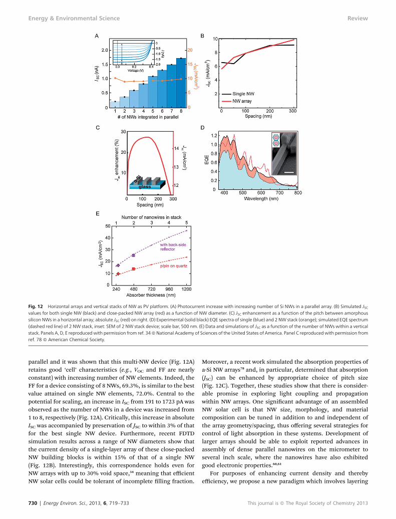
Fig. 12 Horizontal arrays and vertical stacks of NW as PV platform. (A) Photocurrent increase with increasing number of Si NWs in a parallel array. (B) Simulated JSCvalues for both single NW (black) and close-packed NW array (red) as a function of NW diameter. (C) JSC enhancement as a function of the pitch between amorphoussilicon NWs in a horizontal array; absolute JSC (red) on right. (D) Experimental (solid black) EQE spectra of single (blue) and 2 NW stack (orange); simulated EQE spectrum(dashed red line) of 2 NW stack, inset: SEM of 2 NW stack device; scale bar, 500 nm. (E) Data and simulations of JSC as a function of the number of NWs within a verticalstack. Panels A, D, E reproduced with permission from ref. 34ªNational Academy of Sciences of the United States of America. Panel C reproducedwith permission fromref. 78 ª American Chemical Society.
Energy & Environmental Science Review
parallel and it was shown that this multi-NW device (Fig. 12A)retains good ‘cell’ characteristics (e.g., VOC and FF are nearlyconstant) with increasing number of NW elements. Indeed, theFF for a device consisting of 8 NWs, 69.3%, is similar to the bestvalue attained on single NW elements, 72.0%. Central to thepotential for scaling, an increase in ISC from 191 to 1723 pA wasobserved as the number of NWs in a device was increased from1 to 8, respectively (Fig. 12A). Critically, this increase in absoluteISC was accompanied by preservation of JSC to within 3% of thatfor the best single NW device. Furthermore, recent FDTDsimulation results across a range of NW diameters show thatthe current density of a single-layer array of these close-packedNW building blocks is within 15% of that of a single NW(Fig. 12B). Interestingly, this correspondence holds even forNW arrays with up to 30% void space,34 meaning that efficientNW solar cells could be tolerant of incomplete lling fraction.
730 | Energy Environ. Sci., 2013, 6, 719–733
Moreover, a recent work simulated the absorption properties ofa-Si NW arrays78 and, in particular, determined that absorption(JSC) can be enhanced by appropriate choice of pitch size(Fig. 12C). Together, these studies show that there is consider-able promise in exploring light coupling and propagationwithin NW arrays. One signicant advantage of an assembledNW solar cell is that NW size, morphology, and materialcomposition can be tuned in addition to and independent ofthe array geometry/spacing, thus offering several strategies forcontrol of light absorption in these systems. Development oflarger arrays should be able to exploit reported advances inassembly of dense parallel nanowires on the micrometer toseveral inch scale, where the nanowires have also exhibitedgood electronic properties.60,61
For purposes of enhancing current density and therebyefficiency, we propose a new paradigm which involves layering
This journal is ª The Royal Society of Chemistry 2013
Review Energy & Environmental Science
and interconnecting optimized core/multi-shell NW compo-nents. Demonstrating the potential of this new concept, recentwork has shown how a well-aligned vertical stack of 2 p/pincore–shell NWs can be assembled on a quartz substrate andconnected electrically in parallel (Fig. 12D, inset). Transportmeasurements for such a device yield a JSC of 14.0 mA cm�2, a1.4� increase compared to the best single NW device. Signi-cantly, the experimental EQE spectrum for this double NWdevice (Fig. 12D) shows that peaks coincide in wavelength withthose for a single NW device and that EQE amplitudes for theformer are increased by a factor of 1.0–2.0 across the spectrum.Notably, FDTD simulations reproduce the EQE enhancementfor the double NW stack conguration and predict a compa-rable 41% increase in JSC. Finally, additional simulations haveshown that a layered stack of ve NWs can yield JSC values of 24and >40 mA cm�2 without and with a back-side reector,respectively (Fig. 12E). These values coupled with the high VOCvalues reported for the single core/multi-shell NW devices(Section 5), which have been shown to be preserved uponparallel integration (Fig. 12A), could yield power-conversionefficiencies >15%.
8 Conclusions and prospects for futureresearch
Moving forward into the future there are substantial opportu-nities in a number of areas, including (i) the synthesis of newnanoscale materials with enhanced photovoltaic proper-ties,34,59,94 (ii) the development of robust methods for large-scaleassembly needed to produce the arrays necessary for large-scalephotovoltaic applications, and (iii) the exploration and devel-opment of self-powered nanosystems.36 First, in addition to thenovel synthetic directions outlined in this review, there existsubstantial opportunities in exploring more complexmorphologies as well as heteroepitaxial growth to furtherenhance light-absorption and open circuit voltages in sub-wavelength NW structures. NW design96 and synthesis effortsshould also address more practical issues such as NW size anddoping heterogeneity, because variations in these parameterscan limit the power conversion efficiency of the system.97 Othersynthetic advances, including nanowire growth by aerotaxy98
and lower temperature processes,52 may also enable costreductions of the building blocks. Second, while existingtransfer techniques60,61,95 can pattern NWs over large-areas andat high density, yet additional improvements and/or newmethods allow assembly independent of NW size ormorphology, reduce packing defects in assembled arrays, andallow for end-to-end registry. These features, when combined,could facilitate large arrays and ultimate manufacturing of NWsolar cells. Third, and independent of these further improve-ments needed for commercially viable solar cells, we stress thata growing opportunity exists for exploiting the power-genera-tion now available from NW PVs for self-powered nanosystems,including nanosensors, which might be embedded in thehuman body for continuously monitoring health, andnanoprocessors.36
This journal is ª The Royal Society of Chemistry 2013
References
1 International Energy Outlook 2011, U. S. Energy InformationAdministration, 2011.
2 Renewables 2011, Global Status Report, Renewable EnergyPolicy Network, 2011.
3 D. M. Powell, M. T. Winkler, H. J. Choi, C. B. Simmons,D. B. Needleman and T. Buonassisi, Energy Environ. Sci.,2012, 5, 5874–5883.
4 N. S. Lewis, Science, 2007, 315, 798–801.5 N. S. Lewis and G. Crabtree, Basic Research Needs for SolarEnergy Utilization, U. S. Department of Energy Office ofScience, 2005.
6 Form EIA-63B, Annual Photovoltaic Module/Cell ManufacturersSurvey, U.S. Energy Information Administration, 2006.
7 D. Ginley, M. A. Green and R. Collins, MRS Bull., 2008, 33,355–364.
8 M. A. Green, Third Generation Photovoltaics: Advanced SolarEnergy Conversion, Springer Science, Boston, 2003.
9 Next Generation Photovoltaics: High efficiency through fullspectrum utilization, ed. A. Marti and A. Luque, Institute ofPhysics Publishing, Bristol, 2003.
10 P. V. Kamat, J. Phys. Chem. C, 2008, 112, 18737–18753.11 D. L. Klein, R. Roth, A. K. L. Lim, A. P. Alivisatos and
P. L. McEuen, Nature, 1997, 389, 699–701.12 S. Nie and R. N. Zare, Annu. Rev. Biophys. Biomol. Struct.,
1997, 26, 567–596.13 D. V. Talapin, J. S. Lee, M. V. Kovalenko and
E. V. Shevchenko, Chem. Rev., 2010, 110, 389–458.14 T. W. Odom, J. Huang, P. Kim and C.M. Lieber,Nature, 1998,
391, 62–64.15 H. W. Zhu, J. Q. Wei, K. L. Wang and D. H. Wu, Sol. Energy
Mater. Sol. Cells, 2009, 93, 1461–1470.16 L. B. Hu, D. S. Hecht and G. Gruner, Chem. Rev., 2010, 110,
5790–5844.17 M. S. Fuhrer, J. Nygard, L. Shih, M. Forero, Y. G. Yoon,
M. S. C. Mazzoni, H. J. Choi, J. Ihm, S. G. Louie, A. Zettland P. L. McEuen, Science, 2000, 288, 494–497.
18 M. S. Dresselhaus, G. Dresselhaus, R. Saito and A. Jorio,Phys. Rep., 2005, 409, 47–99.
19 A. H. Castro Neto, F. Guinea, N. M. R. Peres, K. S. Novoselovand A. K. Geim, Rev. Mod. Phys., 2009, 81, 109–162.
20 A. K. Geim, Science, 2009, 324, 1530–1534.21 C. M. Lieber, Solid State Commun., 1998, 107, 607–616.22 J. Hu, T. W. Odom and C. M. Lieber, Acc. Chem. Res., 1999,
32, 435–445.23 X. Duan, Y. Huang, Y. Cui, J. Wang and C. M. Lieber, Nature,
2001, 409, 66–69.24 B. Tian, T. J. Kempa and C. M. Lieber, Chem. Soc. Rev., 2009,
38, 16–24.25 W. Lu and C. M. Lieber, J. Phys. D: Appl. Phys., 2006, 39, 387–
406.26 Y. Li, F. Qian, J. Xiang and C. M. Lieber, Mater. Today, 2006,
9, 18–27.27 L. Lauhon, M. Gudiksen, D. Wang and C. M. Lieber, Nature,
2002, 420, 57–61.28 M. A. Green, Prog. Photovoltaics, 2001, 9, 123–135.
Energy Environ. Sci., 2013, 6, 719–733 | 731

Energy & Environmental Science Review
29 C. Brabec, MRS Bull., 2005, 30, 50–52.30 G. Conibeer, Mater. Today, 2007, 10, 42–50.31 A. Polman and H. A. Atwater, Nat. Mater., 2012, 11, 174–177.32 W. Shockley and H. J. Queisser, J. Appl. Phys., 1961, 32, 510–
519.33 H. Cotal, C. Fetzer, J. Boisvert, G. Kinsey, R. King, P. Hebert,
H. Yoon and N. Karam, Energy Environ. Sci., 2009, 2, 174–192.34 T. J. Kempa, J. F. Cahoon, S.-K. Kim, R. W. Day, D. C. Bell,
H.-G. Park and C. M. Lieber, Proc. Natl. Acad. Sci. U. S. A.,2012, 109, 1407–1412.
35 T. J. Kempa, B. Tian, D. Kim, J. Hu, X. Zheng andC. M. Lieber, Nano Lett., 2008, 8, 3456–3460.
36 B. Tian, X. Zheng, T. J. Kempa, Y. Fang, N. Yu, G. Yu,J. Huang and C. M. Lieber, Nature, 2007, 449, 885–890.
37 B. Tian, T. Cohen-Karni, Q. Qing, X. Duan, P. Xie andC. M. Lieber, Science, 2010, 329, 831–834.
38 T. Cohen-Karni, B. P. Timko, L. E. Weiss and C. M. Lieber,Proc. Natl. Acad. Sci. U. S. A., 2009, 106, 7309–7313.
39 W. Lu, J. Xiang, B. P. Timko, Y. Wu and C. M. Lieber, Proc.Natl. Acad. Sci. U. S. A., 2005, 102, 10046–10051.
40 F. Qian, S. Gradecak, Y. Li, C. Y. Wen and C. M. Lieber, NanoLett., 2005, 5, 2287–2291.
41 C. M. Lieber, MRS Bull., 2003, 28, 486–491.42 J. D. Meindl, Q. Chen and J. A. Davis, Science, 2001, 293,
2044–2049.43 J. R. Heath, P. J. Kuekes, G. S. Snider and R. S. Williams,
Science, 1998, 280, 1716–1721.44 S. W. Boettcher, J. M. Spurgeon, M. C. Putnam, E. L. Warren,
D. B. Turner-Evans, M. D. Kelzenberg, J. R. Maiolo,H. A. Atwater and N. S. Lewis, Science, 2010, 327, 185–187.
45 M. D. Kelzenberg, S. W. Boettcher, J. A. Petykiewicz,D. B. Turner-Evans, M. C. Putnam, E. L. Warren,J. M. Spurgeon, R. M. Briggs, N. S. Lewis andH. A. Atwater, Nat. Mater., 2010, 9, 239–244.
46 B. M. Kayes, H. A. Atwater and N. S. Lewis, J. Appl. Phys.,2005, 97, 114302.
47 M. Law, L. E. Greene, J. C. Johnson, R. Saykally and P. Yang,Nat. Mater., 2005, 4, 455–459.
48 S. M. Sze and K. K. Ng, Physics of Semiconductor Devices, JohnWiley & Sons, Inc., Hoboken, NJ, 2007.
49 A. M. Morales and C. M. Lieber, Science, 1998, 279, 208–211.50 J. L. Liu, S. J. Cai, G. L. Jin, S. G. Thomas and K. L. Wang, J.
Cryst. Growth, 1999, 200, 106–111.51 K. Haraguchi, T. Katsuyama, K. Hiruma and K. Ogawa, Appl.
Phys. Lett., 1992, 60, 745–747.52 J. Tang, Z. Huo, S. Brittman, H. Gao and P. Yang, Nat.
Nanotechnol., 2011, 6, 568–572.53 P. Caroff, K. A. Dick, J. Johansson, M. E. Messing, K. Deppert
and L. Samuelson, Nat. Nanotechnol., 2009, 4, 50–55.54 F. Qian, Y. Li, S. Gradecak, H.-G. Park, Y. Dong, Y. Ding,
Z. L. Wang and C. M. Lieber, Nat. Mater., 2008, 7, 701–706.55 Y. Dong, B. Tian, T. J. Kempa and C. M. Lieber, Nano Lett.,
2009, 9, 2183–2187.56 Y. Li, J. Xiang, F. Qian, S. Gradecak, Y. Wu, H. Yan,
D. A. Blom and C. M. Lieber, Nano Lett., 2006, 6, 1468–1473.
57 F. Dimroth and S. Kurtz, MRS Bull., 2007, 32, 230–235.
732 | Energy Environ. Sci., 2013, 6, 719–733
58 B. Tian, P. Xie, T. J. Kempa, D. C. Bell and C. M. Lieber, Nat.Nanotechnol., 2009, 4, 824–829.
59 S. K. Kim, R. W. Day, J. F. Cahoon, T. J. Kempa, K. Deok,H.-G. Park and C. M. Lieber, Nano Lett., 2012, 12, 4971–4976.
60 Z. Y. Fan, J. C. Ho, Z. A. Jacobson, R. Yerushalmi, R. L. Alley,H. Razavi and A. Javey, Nano Lett., 2008, 8, 20–25.
61 A. Javey, S. W. Nam, R. S. Friedman, H. Yan and C. M. Lieber,Nano Lett., 2007, 7, 773–777.
62 M. D. Kelzenberg, D. B. Turner-Evans, M. C. Putnam,S. W. Boettcher, R. M. Briggs, J. Y. Baek, N. S. Lewis andH. A. Atwater, Energy Environ. Sci., 2011, 4, 866–871.
63 L. G. Jeffery,Handbook of Photovoltaic Science and Engineering,ed. S. Hegedus and A. Luque, Wiley, New York, 2004.
64 P. Wurfel, Physics of Solar Cells, From Principles to NewConcepts, Wiley-VCH Verlag GmbH & Co. KGaA, Weinheim,2005.
65 Y. Ke, X. Weng, J. M. Redwing, C. M. Eichfeld, T. R. Swisher,S. E. Mohney and Y. M. Habib, Nano Lett., 2009, 9, 4494–4499.
66 V. Schmidt, J. V. Wittemann and U. Gosele, Chem. Rev., 2010,110, 361–388.
67 Y. Dan, K. Seo, K. Takei, J. H. Meza, A. Javey andK. B. Crozier, Nano Lett., 2011, 11, 2527–2532.
68 A. Goetzberger, J. Luther and G. Willeke, Sol. Energy Mater.Sol. Cells, 2002, 74, 1–11.
69 O. Klutha, B. Recha, L. Houbena, S. Wiedera, G. Schopea,C. Benekinga, H. Wagnera, A. Lofflb and H. W. Schockb,Thin Solid Films, 1999, 351, 247–253.
70 S. Koynov, M. S. Brandt and M. Stutzmann, Appl. Phys. Lett.,2006, 88, 203107.
71 P. Bermel, C. Luo, L. Zeng, L. C. Kimerling andJ. D. Joannopoulos, Opt. Express, 2007, 15, 16986–17000.
72 J. Zhao and M. A. Green, IEEE Trans. Electron Devices, 1991,38, 1925–1934.
73 S. Chhajed, M. F. Schubert, J. K. Kim and E. F. Schubert,Appl. Phys. Lett., 2008, 93, 251108.
74 R. Corkish, Solar Progress, 1997, 18, 16–17.75 L. Cao, P. Fan, A. P. Vasudev, J. S. White, Z. Yu, W. Cai,
J. A. Schuller, S. Fan and M. L. Brongersma, Nano Lett.,2010, 10, 439–445.
76 L. Cao, J.-S. Park, P. Fan, B. Clemens and M. L. Brongersma,Nano Lett., 2010, 10, 1229–1233.
77 E. S. Barnard, R. A. Pala and M. L. Brongersma, Nat.Nanotechnol., 2011, 6, 588–593.
78 D. Tham and J. R. Heath, Nano Lett., 2010, 10, 4429–4434.79 J. Zhu, C. M. Hsu, Z. Yu, S. Fan and Y. Cui, Nano Lett., 2010,
10, 1979–1984.80 G. Bronstrup, N. Jahr, C. Leiterer, A. Csaki, W. Fritzsche and
S. Christiansen, ACS Nano, 2010, 4, 7113–7122.81 W. F. Liu, J. I. Oh and W. Z. Shen, Nanotechnology, 2011, 22,
125705–125708.82 K. Seo, M. Wober, P. Steinvurzel, E. Schonbrunt, Y. Dan,
T. Ellenbogen and K. B. Crozier, Nano Lett., 2011, 11,1851–1856.
83 L. Novotny and N. van Hulst, Nat. Photonics, 2011, 5, 83–90.84 A. Kinkhabwala, Z. Yu, S. Fan, Y. Avlasevich, K. Mullen and
W. E. Moerner, Nat. Photonics, 2009, 3, 654–657.
This journal is ª The Royal Society of Chemistry 2013
Review Energy & Environmental Science
85 M. D. Kelzenberg, D. B. Turner-Evans, B. M. Kayes,M. A. Filler, M. C. Putnam, N. S. Lewis and H. A. Atwater,Nano Lett., 2008, 8, 710–714.
86 P. L. Gourley, Nature, 1994, 371, 571–577.87 J.-H. Kang, M.-K. Seo, S.-K. Kim, S.-H. Kim, M.-K. Kim,
H.-G. Park, K.-S. Kim and Y.-H. Lee, Opt. Express, 2009, 17,6074–6081.
88 S.-K. Kim, S.-H. Kim, G.-H. Kim, H.-G. Park, D.-J. Shin andY.-H. Lee, Appl. Phys. Lett., 2004, 84, 861–863.
89 B. Cho, J. Bare~no, Y. L. Foo, S. Hong, T. Spila, I. Petrov andJ. E. Greene, J. Appl. Phys., 2008, 103, 123530.
90 H.-Y. Ryu, S.-H. Kim, H.-G. Park, J.-K. Hwang and Y.-H. Lee,Appl. Phys. Lett., 2002, 80, 3883–3885.
91 L. J. Lauhon, M. S. Gudiksen and C. M. Lieber, Philos.Trans.R. Soc., A, 2004, 362, 1247–1260.
This journal is ª The Royal Society of Chemistry 2013
92 L. Cao, J. S. White, J.-S. Park, J. A. Schuller, B. M. Clemensand M. L. Brongersma, Nat. Mater., 2009, 8, 643–647.
93 E. C. Garnett, M. L. Brongersma, Y. Cui and M. D. McGehee,Annu. Rev. Mater. Res., 2011, 41, 269–295.
94 M. J. Bierman and S. Jin, Energy Environ. Sci., 2009, 2, 1050–1059.
95 G. Yu, A. Cao and C. M. Lieber, Nat. Nanotechnol., 2007, 2,372–377.
96 J. D. Christesen, X. Zhang, C. W. Pinion, T. A. Celano,C. J. Flynn and J. F. Cahoon, Nano Lett., 2012, 12, 6024–6029.
97 J. M. Foley, M. J. Price, J. I. Feldblyum and S. Maldonado,Energy Environ. Sci., 2012, 5, 5203–5220.
98 M. Heurlin, M. H. Magnusson, D. Lindgren, M. Ek,L. R. Wallenberg, K. Deppert and L. Samuelson, Nature,2012, 492, 90–94.
Energy Environ. Sci., 2013, 6, 719–733 | 733