engineering design progress report
TRANSCRIPT

Portland State University
Winter 2011
JTAG Connector Engineering Design Progress Report
March 7, 2011
A Joint Project with the
Intel Corporation Hawthorn Farm Campus
Group members:
David Stepnowski
Jeremiah Martin
Khaled Alshaiban
Long Nguyen
Tinh Tran
Intel Sponsors:
Michelle L. Seale
Frank W. Joyce
PSU Advisor: Chien Wern
1
Executive Summary
The JTAG project was proposed to the Mechanical Engineering Department at PSU by
Intel. Its objective is to design a hand operated device that can reduce the connecting time
between a JTAG testing board and a test circuit board. Intel currently employs a process
which involves attaching a small testing circuit board, called a surfboard, and block of
contact pins using nuts and bolts for attachment to the circuit board to be tested. This
process takes three to four minutes. A reduction of the overall connecting time to less
than 30 seconds is desired. There is very little space available near the pad contact area of
the circuit boards to be tested, which acts as an important constraint on possible designs.
The following document outlines the progress of the JTAG project and describes the
design process that the JTAG team has followed.
The JTAG capstone team has completed the following: a Product Design Specification
(PDS) document, internal and external research, and concept evaluation and selection. All
milestones were achieved on time. The external research was performed to identify any
related products and to quantify their ability to meet the design criteria outlined in the
PDS report. None of the products identified in the external research were capable of
meeting all the necessary requirements. The internal research phase yielded 17 concepts.
Concept screening, evaluation, and selection processes were preformed to reduce the
original 17 designs down to one. The Holding Block design received the highest ratings
in the selection process and was selected to move onto the detailed design phase. The
Holding Block design will incorporate the surfboard and pin block components that are
used in the current process.
The Holding block design concept is in compliance with the PDS document. The design
is expected to: have an application time of less than 30 seconds, exceed the life cycle
target of 1000 duty cycles, require no maintenance over the life cycle, and provide a
consistent and evenly distributed contact force. A simplified model of the selected design
was presented to the customer at Intel and was well received.
2
Contents
EXECUTIVE SUMMARY .......................................................................... 1
INTRODUCTION ........................................................................................ 3
MISSION STATEMENT ............................................................................. 4
PROJECT PLAN .......................................................................................... 4
PDS SUMMARY ........................................................................................... 5
EXTERNAL SEARCH................................................................................. 5
INTERNAL SEARCH .................................................................................. 7
TOP LEVEL DESIGN EVALUATION ................................................... 77
DETAILED DESIGN PROGRESS........................................................... 11
CONCLUSION ........................................................................................... 12
BIBLIOGRAPHY ....................................................................................... 14
APPENDICES ............................................................................................ 14

3
Introduction
JTAG, also known as boundary-scan, is a name given to the IEEE 1149.1 standard (1).
The name is taken from Joint Test Action Group, the body that originally created the
standard (2). JTAG is used for board level testing.
The current method in use at Intel to make board connections for JTAG testing involves
the installation of a small circuit board (called a surfboard) to the device under test
(DUT). There are two disadvantages of this method that are desirable to improve. Firstly,
the surfboard is attached to the DUT with screws and nuts, which require the operator to
use a screwdriver to remove the surfboard after every PCB (printed circuit board) is
tested. Some DUTs are composed of two printed circuit boards clamped together by nuts
and bolts, so they also need to be disassembled before the surfboard can be connected.
This installation and removal process is considered overly time consuming. Secondly, the
assembly includes many small components that have a possibly of being misplaced.
Therefore, the objective of this project is to produce a prototype that will decrease the
connection/disconnection time and reduce the probability of lost components while
maintaining signal integrity. The JTAG connector must also be capable of attaching to a
variety of PCB assemblies as shown in Figure 1.
Figure 1: Shows the current method used to fasten a JTAG Surfboard to a bi-level PCB
test assembly.
PCB Fasteners
Surfboard
DUT Fasteners
4
Mission statement
The JTAG capstone team will design a small hand operated device that will attach testing
connectors to a circuit board. The time to apply or remove the testing connectors must be
shorter than the currently employed methods. This device should not require operator
assembly to function and needs to provide sufficient contact force to maintain signal
integrity between the surfboard and the test PCB. This device must not interfere with any
existing components on the circuit board and must meet Intel’s ergonomic requirements.
A working prototype of the connector will be delivered to Intel’s representatives no later
than June 2011.
Project Plan
The following project milestones have been completed: PDS report, external/internal
research and final concept evaluation. The next phase of the project is detailed design.
During this phase of the project the final selected design will be broken down into
functional subsystems. Each one of these subsystems will be subject to an individual
engineering design optimization process. Models of these detailed designs will be created
in a 3D format using the CAD software, SolidWorks. These solid models will be utilized
in the fabrication of the first prototypes. System level detailed designs are to be finished
and discussed with the sponsors by April 12th. The first prototypes are to be fabricated
no later than April 28th, allowing time for design optimization, revision and testing. The
final prototype design will be accompanied by a user's guide and other documentation
that outlines the functional specifications for the JTAG connector. The deliverables will
be handed over to the project team sponsors at Intel during the week of June 13th, 2011.
The project schedule may be subject to change, if unforeseen complications arise.
Currently, the project is on schedule and within budget.
5
PDS Summary
The purpose of the Product Design Specification (PDS) is to focus the efforts of the
design team on creating a product that best suits the customer's needs. The PDS report is
referenced at every step of the design process to validate design decisions and create
design evaluation and selection metrics. Adhering to the process of referencing the PDS,
making design decisions, and validating design decisions will ensure a prototype of the
JTAG connector that should meet and/or exceed all the customer's needs. A summary of
the Product Design Specification table can be found in Appendix 1.
External Search
The external search presented a wide range of solutions to the JTAG connecter issue. An
external search was performed to indentify competing and related products. Currently,
there are many products which are designed to provide electrical connections between
printed circuit boards. The following are three examples of devices found:
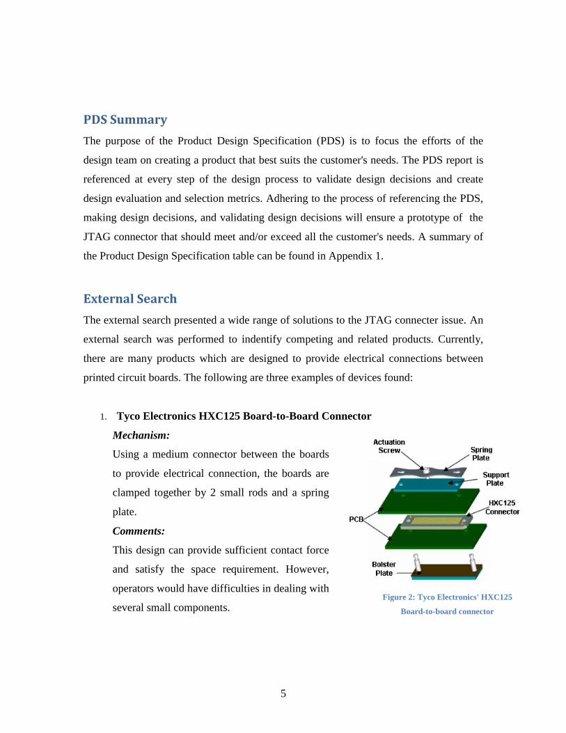
1. Tyco Electronics HXC125 Board-to-Board Connector
Mechanism:
Using a medium connector between the boards
to provide electrical connection, the boards are
clamped together by 2 small rods and a spring
plate.
Comments:
This design can provide sufficient contact force
and satisfy the space requirement. However,
operators would have difficulties in dealing with
several small components.
Figure 2: Tyco Electronics' HXC125
Board-to-board connector
6
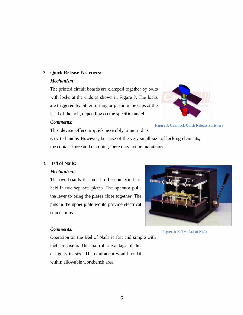
2. Quick Release Fasteners:
Mechanism:
The printed circuit boards are clamped together by bolts
with locks at the ends as shown in Figure 3. The locks
are triggered by either turning or pushing the caps at the
head of the bolt, depending on the specific model.
Comments:
This device offers a quick assembly time and is
easy to handle. However, because of the very small size of locking elements,
the contact force and clamping force may not be maintained.
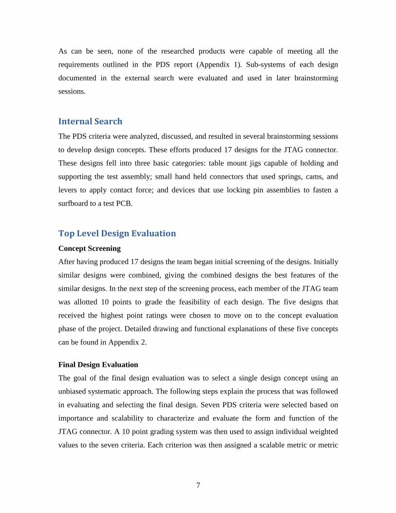
3. Bed of Nails:
Mechanism:
The two boards that need to be connected are
held in two separate plates. The operator pulls
the lever to bring the plates close together. The
pins in the upper plate would provide electrical
connections.
Comments:
Operation on the Bed of Nails is fast and simple with
high precision. The main disadvantage of this
design is its size. The equipment would not fit
within allowable workbench area.
Figure 3: Cam-lock Quick Release Fasteners
Figure 4: X-Test Bed of Nails
7
As can be seen, none of the researched products were capable of meeting all the
requirements outlined in the PDS report (Appendix 1). Sub-systems of each design
documented in the external search were evaluated and used in later brainstorming
sessions.
Internal Search
The PDS criteria were analyzed, discussed, and resulted in several brainstorming sessions
to develop design concepts. These efforts produced 17 designs for the JTAG connector.
These designs fell into three basic categories: table mount jigs capable of holding and
supporting the test assembly; small hand held connectors that used springs, cams, and
levers to apply contact force; and devices that use locking pin assemblies to fasten a
surfboard to a test PCB.
Top Level Design Evaluation
Concept Screening
After having produced 17 designs the team began initial screening of the designs. Initially
similar designs were combined, giving the combined designs the best features of the
similar designs. In the next step of the screening process, each member of the JTAG team
was allotted 10 points to grade the feasibility of each design. The five designs that
received the highest point ratings were chosen to move on to the concept evaluation
phase of the project. Detailed drawing and functional explanations of these five concepts
can be found in Appendix 2.
Final Design Evaluation
The goal of the final design evaluation was to select a single design concept using an
unbiased systematic approach. The following steps explain the process that was followed
in evaluating and selecting the final design. Seven PDS criteria were selected based on
importance and scalability to characterize and evaluate the form and function of the
JTAG connector. A 10 point grading system was then used to assign individual weighted
values to the seven criteria. Each criterion was then assigned a scalable metric or metric
8
system. The following list shows the seven PDS criteria that were selected, their
individual weights, and associated metric or metric system:
Application Time; Estimated time spent by an operator to apply the JTAG
connector.
o Weight: 3.5
o Metric: The PDS criteria target requires an application time of less than 30
seconds. Each team member was timed while acting out a mock assembly
process. Their times were normalized with the PDS target value of 30
seconds. This quotient was then subtracted from 1 and then multiplied by
5 to arrive at score.
Ease of Use: Educated guess as to the operational ease of use.
o Weight: 1.5
o Metric: This criterion was broken down into 3 sub-categories:
A.) Required effort to operate the connector (e.g. repetitive motion
or application of excessive force).
B.) Effort spent on locating the board in the device and aligning
the connection holes.
C.) Accessibility to the DUT after assembly for further testing.
The three sub categories were given individual weighted values
based on a 5 point scale. The weighted values of the three sub-
categories are (A = 2), (B = 3), and (C = 4).
o Each design concept was evaluated using the 3 sub-categories and
received 0-5 points, 5 being the best grade. The 3 sub-category point
values were summed and divided by 15. This normalized point value was
then multiplied by 5 to get a total score for the main Ease of use criterion.
Life Cycle: The ability of the connector to meet or exceed the PDS target of 1000
cycles before replacement.
o Weight: 1.04
o Metric: A thought experiment was done on each of the design concepts to
determine likely points of failure. The JTAG team members then assigned
9
each design concept a value of 1-5. A score of 5 indicating that a design
would be less likely to fail during the first 1000 operational cycles.
Supports the Weight of the Test Assembly: The ability of the design concept to
support the weight of the PCB without causing damage to any part of the
assembly.
o Weight: 0.72
o Metric: A thought experiment was done for each concept design to
determine the likelihood of catastrophic failure in the connector. The
JTAG team members then assigned each concept design a value of 1-5. A
point value of 5 subjectively indicating a design that is impervious to
catastrophic failure.
Cost: The cost of prototyping, and manufacturing.
o Weight: 1.0
o Metric: The total cost is broken down into two categories: prototype cost,
and manufacturing cost.
Prototype Cost: Assumptions #1:
Shop or machining time cost $100 per hour.
Each machined feature takes 15 minutes to complete.
Refer to Appendix 4 for an example of the cost calculation.
Manufacturing Costs: Assumptions #2:
Costs are proportional to the prototyping cost depending on
the manufacturing processes involved in mass production.
The proportionality constant is a value of = 0.1 to 1. A
value of = 1 would indicate that each new connector
would cost as much as the first to manufacture.
The grading of the Cost criteria for each of the design
concepts is completed by first calculating the prototyping
cost using Assumption #1. The manufacturing cost is then
calculated by finding the product of the prototyping cost
and the manufacturing cost proportionality constant ( )
using Assumption #2. The sum of the prototyping cost and
10
manufacturing cost is given a relative score of 1 to 5. A
score of 5 indicating that the design will be relatively
inexpensive compared to the other designs. Refer to
Appendix 4 for an example of the total cost calculation.
Maintenance: Whether or not the design concept will require maintenance before
its life cycle is complete.
o Weight: 0.64
o Metric: A thought experiment was done on each of the design concepts to
determine the likelihood of required maintenance. Factors taken into
consideration during the thought experiment were: number of total parts,
number of moving parts, durability of design, and materials used in
construction. A subjective value of 1 through 5 was given to each of the
designs. A value of 5 indicating that the design concept would not require
maintenance.
Contact Force: The criterion was subdivided into two separate categories:
consistency and distribution. Each sub-category was weighted evenly
o Weight: 1.6
o Metric: Consistency and Distribution
Consistency refers the ability of the design concept to apply a
consistence force over the life cycle of the connector.
Distribution refers to the ability of the design concept to apply an
evenly distributed load over the contact area.
The JTAG team members then assigned each design concept a
value of 1-5 for each sub-category. The sum of the two sub-
categories scores was normalized and multiplied by 5. A high
score of 5 for this criterion indicates that the design applies a
constant, evenly distributed contact force over the contact area. A
low score for this criterion indicates that the design could apply an
inconsistent contact force, or one away from the pad area.
11
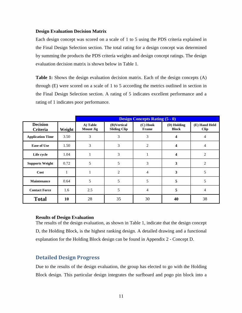
Design Evaluation Decision Matrix
Each design concept was scored on a scale of 1 to 5 using the PDS criteria explained in
the Final Design Selection section. The total rating for a design concept was determined
by summing the products the PDS criteria weights and design concept ratings. The design
evaluation decision matrix is shown below in Table 1.
Table 1: Shows the design evaluation decision matrix. Each of the design concepts (A)
through (E) were scored on a scale of 1 to 5 according the metrics outlined in section in
the Final Design Selection section. A rating of 5 indicates excellent performance and a
rating of 1 indicates poor performance.
Design Concepts Rating (5 - 0)
Decision
Criteria Weight A) Table
Mount Jig (B)Vertical
Sliding Clip (C) Hook
Frame (D) Holding
Block (E) Hand Held
Clip
Application Time 3.50 3 3 3 4 4
Ease of Use 1.50 3 3 2 4 4
Life cycle 1.04 1 3 1 4 2
Supports Weight 0.72 5 5 3 3 2
Cost 1 1 2 4 3 5
Maintenance 0.64 5 5 5 5 5
Contact Force 1.6 2.5 5 4 5 4
Total 10 28 35 30 40 38
Results of Design Evaluation
The results of the design evaluation, as shown in Table 1, indicate that the design concept
D, the Holding Block, is the highest ranking design. A detailed drawing and a functional
explanation for the Holding Block design can be found in Appendix 2 - Concept D.
Detailed Design Progress
Due to the results of the design evaluation, the group has elected to go with the Holding
Block design. This particular design integrates the surfboard and pogo pin block into a
12
holding block. The connecting pins are held in the locked position by springs. The
operator pulls up on the control knob thereby creating a gap for the PCB to be inserted.
The block is then aligned with the PCB holes and the control knob is released. A pressure
plate pushes down on the surfboard and pogo pin assembly with the required contact
force.
Several issues will be resolved during the detail design process. The block shape will be
modified to allow for connection of the test cables to the surfboard. The control knob will
be properly sized to meet Intel’s ergonomic standards. An external search will be
performed to identify any possible off the shelf components which could reduce the total
cost of the prototype. Failure points in the design will be analyzed to determine if stress
reduction is possible. The materials used in the Holding Block design will be analyzed
for mechanical and electrical properties, performance, and cost.
To optimize the overall performance of the JTAG holding block, the design will be
decomposed into 5 subsystems. Each subsystem will checked against the PDS criteria
and analyzed, as necessary, for purposes of material selection and possible form changes.
Effects of variations in dimensions and geometry will be considered for purposes of
tolerancing. Small scale changes to the parts and subsystems will be considered to better
meet PDS requirements.
Conclusion
The JTAG project is up to date and on schedule up through the Concept Evaluation and
Selection phase. A Product Design Specification or PDS report was developed to address
design criteria, customer requirements and priorities. This document has been used as a
guideline for any decisions made in the steps that follow.
In the external search phase of the project, many board to board connectors were studied.
The external search verified that an off the shelf, hand-operated connector which meets
the requirements defined in the PDS report is not available on the market. Therefore, a
design for an original JTAG connector is necessary.
13
In the internal search phase of the project, 17 concepts were generated; five of which
were chosen to be evaluated. The seven decision criteria selected from the PDS in order
of importance are: application time, contact force, ease of use, life cycle, ability to
support board weight, cost (exclude operation time), and maintenance. The seven criteria
were used in a decision matrix to select the final design, Holding Block (Appendix 2 –
Concept D).
The Holding Block design concept was checked against the PDS report to assure full
compliance. The Holding Block design exceeds many of the PDS target guidelines:
reduces application by an estimated 20 seconds, expected to meet and exceed the life
cycle target of 1000 duty cycles, require little or no maintenance over the design's life
cycle, and provide a consistent and evenly distributed contact force. A simplified model
of the final design was presented, explained and well received by the customers at Intel.
The next phase of the JTAG project will be detail design, modeling, prototyping, and
testing. During the detail design of Holding Block, it will be decomposed into functional
subsystems which will be analyzed for optimization. Each subsystem will be subject to an
individual design process before a full design is created. Finally, the working prototype
will be fabricated for testing and validation. The complete prototype and all
documentations are expected to be delivered to the customer by June 2011.

14
Bibliography
1. Corelis Inc. JTAG Tutorial. www.corelis.com. [Online] 2010.
www.corelis.com/education/JTAG_Tutorial.htm.
2. Texas Instruments. IEEE Std 1149.1 (JTAG) Testability. 1997.
3. Intel Inc. Ergonomics Design Guidelines & Assessment Methods. 2009.
15
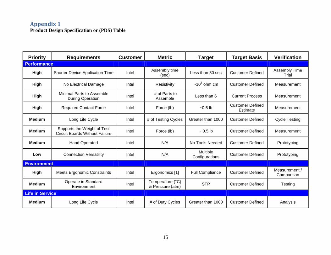
Appendix 1 Product Design Specification or (PDS) Table
Priority Requirements Customer Metric Target Target Basis Verification
Performance
High Shorter Device Application Time Intel Assembly time
(sec) Less than 30 sec Customer Defined
Assembly Time Trial
High No Electrical Damage Intel Resistivity ~108 ohm cm Customer Defined Measurement
High Minimal Parts to Assemble
During Operation Intel
# of Parts to Assemble
Less than 6 Current Process Measurement
High Required Contact Force Intel Force (lb) ~0.5 lb Customer Defined
Estimate Measurement
Medium Long Life Cycle Intel # of Testing Cycles Greater than 1000 Customer Defined Cycle Testing
Medium Supports the Weight of Test
Circuit Boards Without Failure Intel Force (lb) ~ 0.5 lb Customer Defined Measurement
Medium Hand Operated Intel N/A No Tools Needed Customer Defined Prototyping
Low Connection Versatility Intel N/A Multiple
Configurations Customer Defined Prototyping
Environment
High Meets Ergonomic Constraints Intel Ergonomics [1] Full Compliance Customer Defined Measurement /
Comparison
Medium Operate in Standard
Environment Intel
Temperature (°C) & Pressure (atm)
STP Customer Defined Testing
Life in Service
Medium Long Life Cycle Intel # of Duty Cycles Greater than 1000 Customer Defined Analysis
16
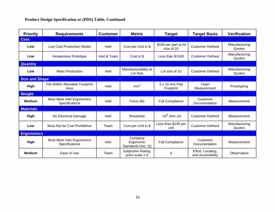
Product Design Specification or (PDS) Table, Continued
Priority Requirements Customer Metric Target Target Basis Verification
Cost
Low Low Cost Production Model Intel Cost per Unit in $ $100 per part at lot
size of 10 Customer Defined
Manufacturing Quotes
Low Inexpensive Prototype Intel & Team Cost in $ Less than $1500 Customer Defined Manufacturing
Quotes
Quantity
Low Mass Production Intel Manufacturability at
Lot Size Lot size of 10 Customer Defined
Manufacturing Quotes
Size and Shape
High Fits Within Allowable Footprint
Area Intel mm
2
5 x 10 mm Pad Footprint
Team Measurement
Prototyping
Weight
Medium Must Meet Intel Ergonomics
Specifications Intel Force (lb) Full Compliance
Customer Documentation
Measurement
Materials
High No Electrical Damage Intel Resistivity ~108 ohm cm Customer Defined Measurement
Low Must Not be Cost Prohibitive Team Cost per Unit in $ Less than $100 per
unit Customer Defined
Manufacturing Quotes
Ergonomics
High Must Meet Intel Ergonomics
Specifications Intel
Company Ergonomic
Standards Doc. [1] Full Compliance
Customer Documentation
Measurement
Medium Ease of Use Team Subjective Rating:
point scale 1-5 5
Effort, Locating, and Accessibility
Observation

17
Product Design Specification or (PDS) Table, Continued
Priority Requirements Customer Metric Target Target Basis Verification
Quality and Reliability
Medium Requires no Maintenance Intel N/A No Maintenance Customer Defined Manufacturing
Quotes
Medium Supports the Weight of Test
Circuit Boards Intel Pounds (lb)
Greater than or equal to 0.5 lb
Customer Defined Measurement
Disposal
Low Creates no Disposables Until
Life Cycle is Complete Intel Life Cycle
Greater than 1000 Cycles
Customer Defined Testing
Documentation
High Final Report PSU Due Date June-2011 PSU Grading
High 3D Models and Drawings Intel Project Completion June-2011 PSU Receipt
Medium PDS PSU Due Date February 9th PSU Grading
Medium Progress Report PSU Due Date March 7th PSU Grading
18
Appendix 2
Internal Search Concepts
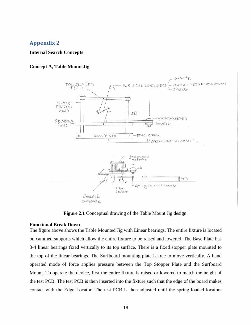
Concept A, Table Mount Jig
Figure 2.1 Conceptual drawing of the Table Mount Jig design.
Functional Break Down
The figure above shows the Table Mounted Jig with Linear bearings. The entire fixture is located
on cammed supports which allow the entire fixture to be raised and lowered. The Base Plate has
3-4 linear bearings fixed vertically to its top surface. There is a fixed stopper plate mounted to
the top of the linear bearings. The Surfboard mounting plate is free to move vertically. A hand
operated mode of force applies pressure between the Top Stopper Plate and the Surfboard
Mount. To operate the device, first the entire fixture is raised or lowered to match the height of
the test PCB. The test PCB is then inserted into the fixture such that the edge of the board makes
contact with the Edge Locator. The test PCB is then adjusted until the spring loaded locators
19
slide into the PCB's test port holes. Once the test PCB is in place the Surf Board assembly is
clamped down into position via a lever mechanism, gravity, spring assembly, or other force
applying device.
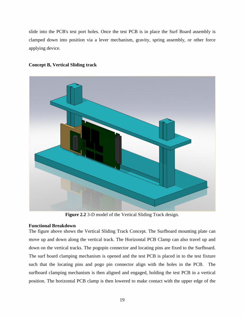
Concept B, Vertical Sliding track
Figure 2.2 3-D model of the Vertical Sliding Track design.
Functional Breakdown
The figure above shows the Vertical Sliding Track Concept. The Surfboard mounting plate can
move up and down along the vertical track. The Horizontal PCB Clamp can also travel up and
down on the vertical tracks. The pogopin connector and locating pins are fixed to the Surfboard.
The surf board clamping mechanism is opened and the test PCB is placed in to the test fixture
such that the locating pins and pogo pin connector align with the holes in the PCB. The
surfboard clamping mechanism is then aligned and engaged, holding the test PCB in a vertical
position. The horizontal PCB clamp is then lowered to make contact with the upper edge of the
20
test PCB. This contact should apply enough force to hold the test PCB in place for the duration
of the test. The surfaces that contact the edges of the test PCB will be covered with a non
conductive rubber like material. The clamping mechanism could utilize a spring clip, hinge and
spring setup, variable height knob, cammed leaver, or other clamping force device.
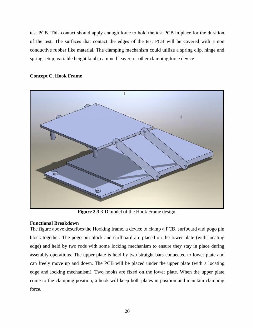
Concept C, Hook Frame
Figure 2.3 3-D model of the Hook Frame design.
Functional Breakdown
The figure above describes the Hooking frame, a device to clamp a PCB, surfboard and pogo pin
block together. The pogo pin block and surfboard are placed on the lower plate (with locating
edge) and held by two rods with some locking mechanism to ensure they stay in place during
assembly operations. The upper plate is held by two straight bars connected to lower plate and
can freely move up and down. The PCB will be placed under the upper plate (with a locating
edge and locking mechanism). Two hooks are fixed on the lower plate. When the upper plate
come to the clamping position, a hook will keep both plates in position and maintain clamping
force.
21
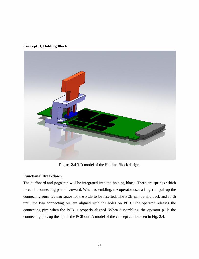
Concept D, Holding Block
Figure 2.4 3-D model of the Holding Block design.
Functional Breakdown
The surfboard and pogo pin will be integrated into the holding block. There are springs which
force the connecting pins downward. When assembling, the operator uses a finger to pull up the
connecting pins, leaving space for the PCB to be inserted. The PCB can be slid back and forth
until the two connecting pin are aligned with the holes on PCB. The operator releases the
connecting pins when the PCB is properly aligned. When dissembling, the operator pulls the
connecting pins up then pulls the PCB out. A model of the concept can be seen in Fig. 2.4.
22
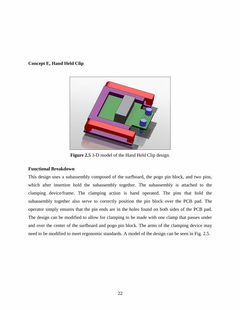
Concept E, Hand Held Clip
Figure 2.5 3-D model of the Hand Held Clip design.
Functional Breakdown
This design uses a subassembly composed of the surfboard, the pogo pin block, and two pins,
which after insertion hold the subassembly together. The subassembly is attached to the
clamping device/frame. The clamping action is hand operated. The pins that hold the
subassembly together also serve to correctly position the pin block over the PCB pad. The
operator simply ensures that the pin ends are in the holes found on both sides of the PCB pad.
The design can be modified to allow for clamping to be made with one clamp that passes under
and over the center of the surfboard and pogo pin block. The arms of the clamping device may
need to be modified to meet ergonomic standards. A model of the design can be seen in Fig. 2.5.
23
Appendix 3
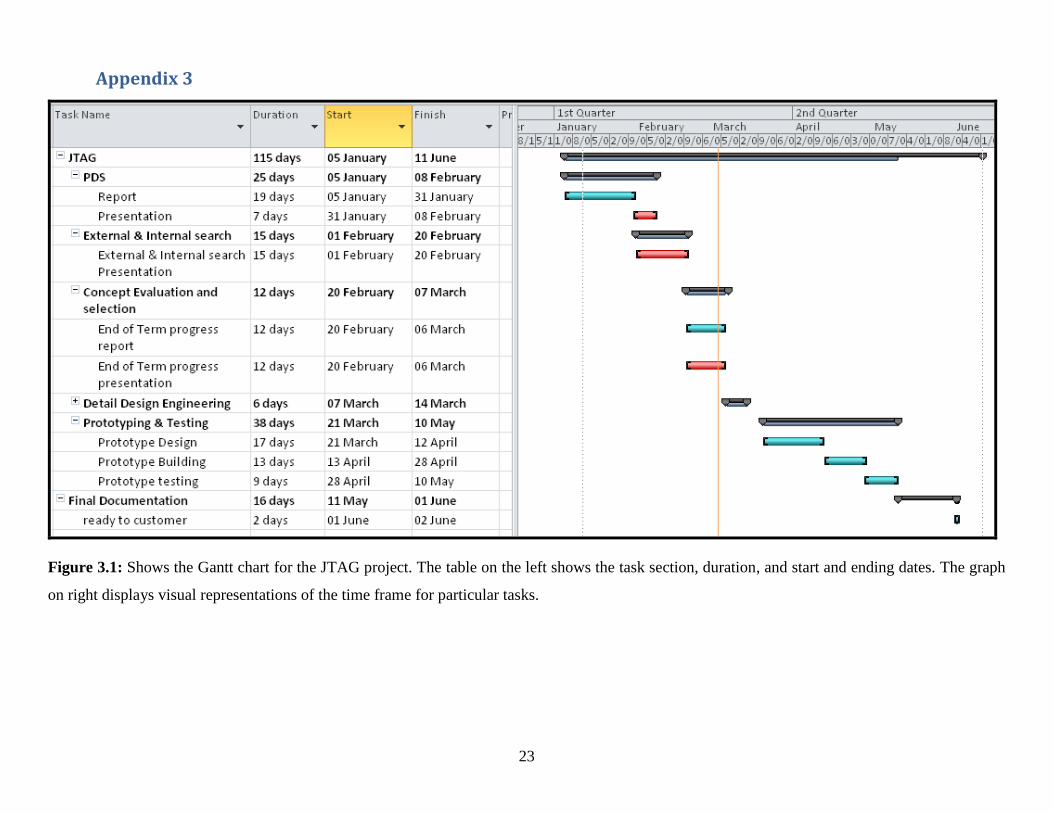
Figure 3.1: Shows the Gantt chart for the JTAG project. The table on the left shows the task section, duration, and start and ending dates. The graph
on right displays visual representations of the time frame for particular tasks.
24
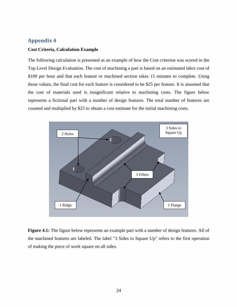
Appendix 4
Cost Criteria, Calculation Example
The following calculation is presented as an example of how the Cost criterion was scored in the
Top Level Design Evaluation. The cost of machining a part is based on an estimated labor cost of
$100 per hour and that each feature or machined section takes 15 minutes to complete. Using
those values, the final cost for each feature is considered to be $25 per feature. It is assumed that
the cost of materials used is insignificant relative to machining costs. The figure below
represents a fictional part with a number of design features. The total number of features are
counted and multiplied by $25 to obtain a cost estimate for the initial machining costs.
Figure 4.1: The figure below represents an example part with a number of design features. All of
the machined features are labeled. The label "3 Sides to Square Up" refers to the first operation
of making the piece of work square on all sides.
2 Holes
1 Ridge
3 Sides to
Square Up
1 Flange
3 Fillets

25
Table 4.1: Shows the total number of features and associated cost
Features Qty. Cost/Feature Cost $
Holes 2 $25 50
Ridges 1 $25 25
Flanges 1 $25 25
Fillets 3 $25 75
Squared Sides 3 $25 75
Total 10 $25 250
As Table 4.1 indicates the estimated initial fabrication cost for the part shown in Figure 4.1 is
$250. The production cost is assumed to be proportional to the initial fabrication cost, materials
used and manufacturing process cost. This proportionality is signified by the constant which
has a value of 0 to 1. A value of = 1 indicates that the production cost is roughly the same as
the initial fabrication cost. For the sake of the costing example it will be assumed that the part
will cost roughly = 1/2 of the initial fabrication cost. The following is an example calculation
used estimate the total cost of production.
Initial fabrication cost = $250
Production Proportionality = 0.5
Lot Size = 10 each
CostTotal _
1500$102505.0250
The estimated total cost to fabricate and produce the part shown in Figure 4.1 is $1500. This
value is by no means representative of the true cost to fabricate and produce the part. This cost
estimating system is only used to compare each of the design cost against each other.