engineering two-dimensional electronics by semiconductor...
TRANSCRIPT

R
E
Da
b
Cc
a
ARRAA
C
h1
Nano Today 16 (2017) 30–45
Contents lists available at ScienceDirect
Nano Today
journa l h om epa ge: www.elsev ier .com/ locate /nanotoday
eview
ngineering two-dimensional electronics by semiconductor defects
an Wanga, Xian-Bin Lia,∗, Dong Hanb, Wei Quan Tianc, Hong-Bo Suna,∗
State Key Laboratory on Integrated Optoelectronics, College of Electronic Science and Engineering, Jilin University, Changchun 130012, ChinaState Key Laboratory of Luminescence and Applications, Changchun Institute of Optics, Fine Mechanics and Physics, Chinese Academy of Sciences,hangchun 130033, ChinaCollege of Chemistry and Chemical Engineering, Chongqing University, Huxi Campus, Chongqing 401331, China
r t i c l e i n f o
rticle history:eceived 19 May 2017eceived in revised form 4 July 2017ccepted 6 July 2017vailable online 25 September 2017
a b s t r a c t
Two-dimensional (2D) semiconductors have attracted considerable attentions from electronic-engineering community due to their unique electronic properties. Especially, the inherent advantageof scaling semiconductor into atomic thickness has raised the prospect of possible extension of theMoore’s law. To achieve 2D electronics, a full comprehension of semiconductor defect physics and chem-istry is indispensable due to its decisive role in controlling electrical performance of 2D materials andfunctionalizing their devices. In this review, first we explain why 2D semiconductors is important fornanoelectronics and optoelectronics. Second, we elucidate how native defects or intentional impuritiesaffect and control electrical characteristic in 2D semiconductors, such as carrier concentration and theirconductive type. In this section, experimental pictures of defects and several updated theoretical methodsto evaluate ionization energies of defects and their conductive type are introduced in detail. Third, typi-
cal device experiments are shown to demonstrate a direct role of defects to functionalize 2D electronicdevice. Furthermore, a database of popular defects and their electrical properties in current popular 2Dsemiconductors is summarized for references. Last, we discuss the challenges and potential prospects ofdefect engineering for 2D devices. The present paper offers important viewpoints from semiconductordefects to design the emerging 2D electronics.© 2017 Elsevier Ltd. All rights reserved.
ontents
Introduction . . . . . . . . . . . . . . . . . . . . . . . . . . . . . . . . . . . . . . . . . . . . . . . . . . . . . . . . . . . . . . . . . . . . . . . . . . . . . . . . . . . . . . . . . . . . . . . . . . . . . . . . . . . . . . . . . . . . . . . . . . . . . . . . . . . . . . . . . . . . . . . 30Experimental characterization of defect . . . . . . . . . . . . . . . . . . . . . . . . . . . . . . . . . . . . . . . . . . . . . . . . . . . . . . . . . . . . . . . . . . . . . . . . . . . . . . . . . . . . . . . . . . . . . . . . . . . . . . . . . . . . . . . . . 32
Atomic resolution imaging . . . . . . . . . . . . . . . . . . . . . . . . . . . . . . . . . . . . . . . . . . . . . . . . . . . . . . . . . . . . . . . . . . . . . . . . . . . . . . . . . . . . . . . . . . . . . . . . . . . . . . . . . . . . . . . . . . . . . . . . . . 32Raman and photoluminescence spectroscopy . . . . . . . . . . . . . . . . . . . . . . . . . . . . . . . . . . . . . . . . . . . . . . . . . . . . . . . . . . . . . . . . . . . . . . . . . . . . . . . . . . . . . . . . . . . . . . . . . . . . . . 34
Theoretical evaluation on carrier ionization energy of defect for conductivity . . . . . . . . . . . . . . . . . . . . . . . . . . . . . . . . . . . . . . . . . . . . . . . . . . . . . . . . . . . . . . . . . . . . . . . . . 35Ionization energy (evaluated by ground-state electronic structure) . . . . . . . . . . . . . . . . . . . . . . . . . . . . . . . . . . . . . . . . . . . . . . . . . . . . . . . . . . . . . . . . . . . . . . . . . . . . . . . 35The difference between single-particle levels and transition levels . . . . . . . . . . . . . . . . . . . . . . . . . . . . . . . . . . . . . . . . . . . . . . . . . . . . . . . . . . . . . . . . . . . . . . . . . . . . . . . 37Ionization energy (evaluated by transition level) . . . . . . . . . . . . . . . . . . . . . . . . . . . . . . . . . . . . . . . . . . . . . . . . . . . . . . . . . . . . . . . . . . . . . . . . . . . . . . . . . . . . . . . . . . . . . . . . . . 37
Roles of defect in engineering 2D electronic devices . . . . . . . . . . . . . . . . . . . . . . . . . . . . . . . . . . . . . . . . . . . . . . . . . . . . . . . . . . . . . . . . . . . . . . . . . . . . . . . . . . . . . . . . . . . . . . . . . . . . 40Realization of n/p-type conductivity for devices by defect . . . . . . . . . . . . . . . . . . . . . . . . . . . . . . . . . . . . . . . . . . . . . . . . . . . . . . . . . . . . . . . . . . . . . . . . . . . . . . . . . . . . . . . . . 40Device performances associated with defects . . . . . . . . . . . . . . . . . . . . . . . . . . . . . . . . . . . . . . . . . . . . . . . . . . . . . . . . . . . . . . . . . . . . . . . . . . . . . . . . . . . . . . . . . . . . . . . . . . . . . . 41
Conclusion and prospect . . . . . . . . . . . . . . . . . . . . . . . . . . . . . . . . . . . . . . . . . . . . . . . . . . . . . . . . . . . . . . . . . . . . . . . . . . . . . . . . . . . . . . . . . . . . . . . . . . . . . . . . . . . . . . . . . . . . . . . . . . . . . . . . . .44Acknowledgements . . . . . . . . . . . . . . . . . . . . . . . . . . . . . . . . . . . . . . . . . . . . . . . . . . . . . . . . . . . . . . . . . . . . . . . . . . . . . . . . . . . . . . . . . . . . . . . . . . . . . . . . . . . . . . . . . . . . . . . . . . . . . . . . . . . . .44References . . . . . . . . . . . . . . . . . . . . . . . . . . . . . . . . . . . . . . . . . . . . . . . . . . . . . . . . . . . . . . . . . . . . . . . . . . . . . . . . . . . . . . . . . . . . . . . . . . . . . . . . . . . . . . . . . . . . . . . . . . . . . . . . . . . . . . . . . . . . . . 44
∗ Corresponding authors.E-mail addresses: [email protected] (X.-B. Li), [email protected] (H.-B. Sun).
ttp://dx.doi.org/10.1016/j.nantod.2017.07.001748-0132/© 2017 Elsevier Ltd. All rights reserved.
Introduction
Two-dimensional (2D) materials are substances with atomicthickness in which electrons are allowed to move freely in 2Dplane but restricted in out-of-plane direction [1–3]. Dimensional-ity reduction brings 2D materials quantum confinement and weak
o Toda
d[otetagdFtpsnisnb[dmid
tTtSsleeegptmedfoetcmotWldsMmnl2pucios(bpF
D. Wang et al. / Nan
ielectric screening which in turn endow them unique properties4–6]. The era of 2D materials begins with the successful isolationf graphene [7]. While it shows great potential in many advancedechnological fields, especially in electronics due to its ultrahighlectron mobility [8,9], the lack of bandgap limits its applica-ion in high-performance filed effect transistors (FETs) [8–10]. Toddress this, researchers make great efforts to open a sizeableap of graphene [11–17]. At the same time, mining 2D semicon-ucting counterparts has also sparked the community’s interests.ollowing graphene, more than ten different layered semiconduc-ors including silicene [18], germanene [19], stanene [20,21], blackhosphorus (BP) [22–24], group-III monochalcogenides [25], tran-ition metal dichalcogenides (TMDs) [26–29], and hexagonal boronitride (BN) [3,30,31] have been successfully prepared by exper-
ments. Their bandgaps range from a few millielectronvolts toeveral electronvolts. Moreover, the band structures depend on theumber of layers [32], such as a transition from indirect gap in theulk MoS2 (1.2 eV) to direct gap in monolayer MoS2 (1.8–2.8 eV)28,33]. In addition, these materials can be stacked layer by layer inesired sequence to create new functional counterparts. Further-ore, the ultrathin nature of 2D semiconductors which allows high
ntegration density has motivated the research in 2D electronicevices.
Following the Moore’s law, the dimensions of FETs continueo decrease [2]. However, FETs cannot be scaled down infinitely.he scaling limitation of Si FETs is predicted to be 5 nanome-ers under which severe short channel effects (SCE) occur [2,34].CE refers to the difficulty of heat dissipation caused by increasedtatic power, which is associated with increased source-to-draineakage current [35,36]. Plentiful researches has been devoted toxplore new channel materials which can mitigate SCE and thenxtend the Moore’s law. In fact, 2D semiconductors are consid-red as one of the most promising candidates due to their excellentate electrostatics and the reduced SCE, which could result in lowerower consumption and high-level device integration [2]. For FETs,he mobile charges distribute widely in three-dimensional (3D)
aterials (Fig. 1(a)) whereas in 2D materials the charged carri-rs are confined in the atomically thin 2D channel with a narrowistribution (Fig. 1(b)). Hence, the carriers are more easily and uni-ormly controlled via gate voltage in 2D materials [37]. On thether hand, Reducing thickness of 3D materials will enhance gatelectrostatic but degrade its FET performance [38]. The degrada-ion comes from the carrier scattering and interface trap statesaused by the undesirable dangling bonds in the surfaces of 3Daterials (see left of Fig. 1(a)). In contrast, 2D materials are free
f dangling bonds (see left of Fig. 1(b)). In fact, MoS2 has beenheoretically predicted to be superior to Si [27,39,40]. With the
entzel-Kramers-Brillouin approximation, Desai et al. [27] calcu-ated the source-to-drain tunneling currents in the OFF state forifferent channel thickness and gate lengths of Si and MoS2, ashown in Fig. 1(c) and (d). For the same gate length (Fig. 1(c)), inoS2, the source-to-drain currents in OFF state are two order ofagnitude smaller than that in silicon. For similar channel thick-
ess (Fig. 1(d)), MoS2 transistor can be scaled to shorter gateength than Si. These results reveal the potential advantages ofD semiconductors as next-generation channel materials for high-erformance devices. More encouragingly, a 1-nm-gate-length FETsing single-walled carbon nanotube as gate and bilayer MoS2 ashannel has been demonstrated at the end of 2016 [27], as shownn Fig. 1(e). It exhibits near ideal switching characteristics with ann-off current ratio of 106 and a subthreshold swing of 65 mV/dec,ee Fig. 1(f). Also, a complementary metal oxide semiconductor
CMOS) technology made from n-type and p-type WSe2 FETs haseen demonstrated [41]. Furthermore, in 2017 Wachter et al. [42]resented a microprocessor consisting of 115 MoS2 transistors, seeig. 1(g). The device shows good operability and then demonstratesy 16 (2017) 30–45 31
the feasibility of using 2D semiconductors to realize complex digitalcircuit.
In addition to the nanoelectronic devices above, 2D semi-conductors also have a potential in optoelectronics [43,44]. p-njunctions, which are the basic building blocks of traditional 3D-semiconductor optoelectronic devices including photodetector,light-emitting diode, and solar cell, have been demonstrated in2D materials. For example, Pospischil et al. [45] reported a lat-eral p-n junction based on electrostatically doped WSe2, as shownin Fig. 2(a). Two splitting gate electrodes are coupled to two dif-ferent regions of a WSe2 flake. Biasing one gate with a positivevoltage and the other with a negative voltage draws electrons andholes into the channel respectively, and thus a p-n junction is real-ized. Under optical illumination, the junctions show photo-voltaicresponse, see the green solid line in Fig. 2(b). Also, Lee et al. [46]realized a vertical p-n junction consisting of monolayer MoS2 (n-type) and WSe2 (p-type) as shown in Fig. 2(c). The metal contactswere fabricated on each layer (D1 and D2 for WSe2; S1 and S2for MoS2), see the bottom right of Fig. 2(c). When the metal elec-trodes D1 (WSe2) and S1 (MoS2) are coupled, the p-n junction isformed between the two 2D semiconductors. The natural n- andp-type channel characteristics of MoS2 and WSe2 are ascribed tothe unintentional doping present in each 2D crystal. They observeda gate-tunable photovoltaic response from the I-Vds curves of thejunction in the gate range of −30 V to 30 V under white-light illumi-nation, as shown in Fig. 2(d)-i. The colour plot of the photocurrentand the photocurrent map of the device are also shown in Fig. 2(d)-ii–iii.
Though 2D materials hold great promise in future electronics,the industrialization of 2D electronic devices faces many chal-lenges. The major one is the development of controllable and stabledoping of 2D semiconductors which must be overcome to real-ize both n-channel and p-channel FETs (two essential componentsfor integrated electronics) just like those in traditional three-dimensional (3D) electronics based on silicon or GaAs. Moreover, ahigh-performance 2D FET requires a low contact resistance whichcan be achieved through degenerate doping in the contact region of2D semiconductors. In addition, optoelectronic devices also requirep-n junctions. As such, defect engineering is indispensable for tai-loring carrier type and concentration of 2D electronic materials andthen facilitate the realization of 2D devices. In addition to the bene-ficial facilitation of offering carriers, defects can also be detrimentalfor device performance as they also can act as undesirable carriertraps, or scattering center, or nonradiative recombination centers.A representative case is the significantly lower electron mobility ofMoS2 reported in experiments than that in theoretical limit, whichmainly points to the mid-gap states induced by defects [47,48]. Infact, 2D materials should be viewed as real materials with defects,rather than perfect 2D layer from the perspective of thermody-namics [49]. Therefore, enhancing our knowledge on the defectphysics of 2D semiconductors should advance the development oflow-power, high-integration electronic devices based on them. Theintentional electronic-properties control for conduction type andconductivity is mainly achieved by engineering point defect (forexample vacancy, substitution, and interstitial). It should be notedthat some large-scale defects such as grain boundary, dislocation,and edges, which may exist in chemically synthesized 2D materi-als, also influence the electronic properties of the materials [50]. Forexample, Zhou et al. [51] discovered two types of 60◦grain bound-aries in MoS2, which introduce dispersive bands crossing the Fermilevel of no-defect MoS2 and then serve as perfect one-dimensionalmetallic quantum wires. In this review, point defects and their
influence on the material properties and device performances aremainly concentrated on.In this review, we will focus on the recent developments ofpoint defect study in 2D semiconductors and their roles on engi-
32 D. Wang et al. / Nano Today 16 (2017) 30–45
Fig. 1. Advantages of 2D semiconductors compared with 3D semiconductors for FETs. Schematic illustration of advantages of 2D materials compared with 3D materials forapplication in FETs: (a) left, 3D semiconductors with reduced thickness, right, gate electrostatics and mobile charge distribution in 3D materials. (b) left, 2D materials, right,gate electrostatics and mobile charge distribution in 2D materials. (c) source-to-drain leakage current ISD-LEAK in the OFF state with Wentzel-Kramers-Brillouin approximationas a function of channel thickness TCH for silicon and MoS2. (d) ISD-LEAK as a function of gate length LG for silicon and MoS2 with different TCH. (e) Schematic of the FET withc cteriso yrightC 7, Nat
neiitetcictccrdTcmo
hannel of bilayer MoS2 and gate of single-walled carbon nanotube. (f) ID-VGS charaf 115 MoS2 transistors. (a) and (b), reprinted with permission from Ref. [37], Copopyright 2016, AAAS. (g), reprinted with permission from Ref. [42], Copyright 201
eering 2D electronic devices. First, the identification of defects byxperimental characterization, including atomic resolution imag-ng observed with electron microscope techniques and structuralnformation probed by Raman and photoluminescence (PL) spec-roscopy, is introduced. Second, the evaluation of defect properties,specially the ability to tune conductivity by two recent developedheoretical methods for carrier ionization from defect in 2D semi-onductors, are clarified. Third, discussions of the role of defectsn electronic device performance including carrier concentration,arrier type, carrier mobility, subthreshold slope, and contact resis-ance, are presented. Fourth, a database including some decisiveharacteristics of frequently studied defects in popular 2D semi-onductors is summarized for references. Finally, we conclude theeview with an outlook for the potential challenges and futureirection of 2D electronics engineered by semiconductor defects.he present review should be useful for the electronic engineering
ommunity and scientists in other field work together to enable theaking and modelling of 2D materials to result in the manufacturef electronic device.
tics of the FET shown in (e). (g) Microscope image of the microprocessor consisting 2014, SPIE Journals and Proceedings. (c)–(f), reprinted with permission Ref. [27],ure Publishing Group.
Experimental characterization of defect
Atomic resolution imaging
Characterization of atomic structures of defects are founda-tions for the exploration of defect behaviors. Knowledge fromatomic resolution imaging of defects is benefit for understanding ofthe material’s properties. Transmission electron microscopy (TEM)and scanning tunneling microscopy (STM) are two main charac-terization tools, furthermore the TEM with equipped aberrationcorrector (AC) have realized atomic resolution [52]. In fact, thenature of down-scaled dimensions in 2D semiconductors enablesmore straightforward insights into atomic structure by the TEM orSTM technique. Here, several typical 2D semiconductors are takenas examples to review the identification of their point defects withAC-TEM or STM. For example, Jin et al. [53] distinguished individ-
ual boron and nitrogen atoms and resolved the intrinsic defects inmonolayer BN by high-resolution TEM (HRTEM). The electron beamirradiation preferentially removes boron atoms resulting in forma-tion of boron vacancies as shown in Fig. 3(a)-i. Accompanied with
D. Wang et al. / Nano Today 16 (2017) 30–45 33
Fig. 2. p-n junction based on 2D semiconductors. (a) Schematic of the WSe2 p-n junction device. Two splitting electrodes are coupled to different regions. Biasing one gatewith a positive voltage and the other with a negative voltage draws electrons and holes into the channel respectively, and thus a p-n junction is realized. (b) I–V characteristicof the p-n junction (VG1 = −40 V, VG2 = 40 V, green solid line) under optical illumination with 1400 Wm−2. Other lines are for different biasing conditions. (c) Bottom left,schematic diagram of a van der Waals heterojunctions. Top, atomic structures of MoS2 and WSe2. Bottom right, optical image of the device. D1 and D2 (S1 and S2) representthe metal contacts of WSe2 (MoS2). When the metal electrodes D1 (WSe2) and S1 (MoS2) are coupled, the p-n junction is formed between the two 2D semiconductors. (d)-i,P (d)-ii,( ermisw
bdi(sovrA
AsseiMm(tpoe
hotoresponse characteristics at different gate voltages under optical illumination;
d)-iii, Photocurrent map of the device presented in (c). (a) and (b), reprinted with pith permission from Ref. [46], Copyright 2014, Nature Publishing Group.
oron vacancies, some larger vacancies in triangle shape are alsoiscriminated. Krivank et al. [52] identified the atomic substitutions
n liquid-phase exfoliated monolayer BN using annular dark-fieldADF) imaging in an AC scanning transmission electron micro-cope (STEM), including carbon substituting for boron/nitrogen andxygen substituting for nitrogen, as shown in Fig. 3(a)-ii. Boronacancies are also identified in bilayer BN (Fig. 3(a)-iii) and theesultant distortions with interlayer bonding are uncovered bylem et al. [54].
Other examples are from the structurally complex TMDs [55,56].mong them, the most popular MoS2 has been experimentallyynthesized by mechanical exfoliation, or chemical vapor depo-ition (CVD), or physical vapor deposition (PVD). Zhou et al. [51]mployed AC-STEM to visualize the intrinsic structural defectsncluding point defects, grain boundaries, and edges in monolayer
oS2 grown by CVD. The commonly observed point defects areonosulfur vacancy VS, disulfur vacancy VS2, multivacancy VMoS3
removing one Mo and its neighboring three S), and another mul-
ivacancy VMoS6 (removing one Mo and its neighboring three Sairs) as shown in Fig. 3(b)-i–iv. Among them, VS is most frequentlybserved. This is consistent with the lowest theoretical formationnergy of VS. Meanwhile, antisite defects are occasionally found inColor plot of the photocurrent as a function of voltages Vds (x axis) and Vg (y axis);sion from Ref. [45], Copyright 2014, Nature Publishing Group. (c) and (d), reprinted
CVD-grown MoS2. Instead, according to the study by Hong et al.[57], antisite defects including MoS (one Mo substituting one Satom, see Fig. 3(b)-v) and MoS2 (one Mo substituting two S atoms,see Fig. 3(b)-vi) are easily observed in PVD grown samples. Theyrevealed that the dominant defect species of monolayer MoS2 issensitive to the growth method and changes from S vacancy in CVDand mechanical exfoliation samples to Mo antisites in PVD samples.Carrying out HRTEM experiments, Komsa et al. [58] showed thatS vacancies including VS and VS2 can be produced under a 80-kVelectron beam irradiation. The further filling of the vacancy siteswith other atomic species is also observed. For intentional doping,Lin et al. [59] demonstrated the successful doping of MoS2 withRe and Au through STEM studies, as can be seen in Fig. 3(c)-i–ii.Re is identified to occupy Mo site whereas Au preferably adsorbson top of Mo, S, or the hollow center. For other candidates in theTMD family, in Nb-doped WS2 Gao et al. [60] identified the posi-tion of Nb sitting at W site (see Fig. 3(d)) with AC-STEM. Cho et al.[61] studied the structural transition in monolayer MoTe2 from
semiconducting hexagonal phase to metallic monoclinic phase. Thetransition is driven by Te vacancy, which is also observed by STEM,see Fig. 3(e). Recently, a new member of the TMDs family, PtSe2also receives significant attention. Wang et al. successfully fabri-
34 D. Wang et al. / Nano Today 16 (2017) 30–45
Fig. 3. Imaging of defects in 2D materials. (a)-i, HRTEM image of boron vacancy in monolayer BN; (a)-ii, TEM image of boron vacancy in bilayer BN; (a)-iii, ADF image of BNdoped by C and O. Red: B; green: N; yellow: C; blue: O. (b)-i–v, STEM-ADF images of intrinsic defects (VS, VS2, VMoS3, VMoS6) in CVD-synthesized MoS2; (b)-v–vi, STEM-ADFimages of intrinsic defects (MoS, MoS2) in PVD-synthesized MoS2. (c)-i and (c)-ii, ADF image of Re-doped and Au-doped MoS2. (d) AC-STEM image of Nb-doped WS2. (e) STEMimage of Te vacancy of MoTe2. (a)-i, reprinted with permission from Ref. [53], Copyright 2009, American Physical Society. (a)-ii, reprinted with permission from Ref. [52],Copyright 2010, Nature Publishing Group. (a)-iii, reprinted with permission from Ref. [54], Copyright 2011, American Physical Society. (b)-i–iv, reprinted with permissionf h permw ed witw
csatfStja2
R
tvr[pTaAwlivab
rom Ref. [51], Copyright 2013, American Chemical Society. (b)-v–vi, reprinted witith permission from Ref. [59], Copyright 2014, Wiley Publishing Group. (d), reprintith permission from Ref. [61], Copyright 2015, AAAS.
ated the monolayer 1T PtSe2 film on a Pt (111) substrate by directelenization [62]. On that basis, Lin et al. [63] demonstrated that
PtSe2 monolayer can be grown in the form of a triangular pat-ern of alternating 1T and 1H phases. The phase transformationrom semiconducting 1T to metallic 1H is also defect-assisted (bye vacancy), which is observed by STM. The intrinsically-grown pat-erned 2D materials potentially provide ideal semiconductor-metalunctions for electronic devices. These characterizations describedbove straightforwardly confirm the existence of various defects inD materials.
aman and photoluminescence spectroscopy
Raman spectroscopy is a popular nondestructive-and-efficientool to detect defects in 2D materials according to the fingerprints ofibrational signals [64]. One of such cases is the well-known defect-elated D and D’ peaks of graphene probed by Raman spectroscopy65]. Another example is that perfect monolayer MoS2 has tworominent Raman-active peaks denoted as E’ and A1
′ [64,66,67].he E’ mode originate from the opposite in-plane vibrations of Mond S atoms (namely, in-plane vibrations of two Mo-S bonds). The1
′ mode corresponds to out-of-plane vibrations of the Mo-S bondsith static center Mo atoms. Parkin et al. [66] observed the evo-
ution of the Raman modes with varying amounts of S vacancy
nduced by electron beam irradiation. They found that when Sacancies are induced, the peaks of E’ and A1′ behave redshiftnd blueshift, respectively, see Fig. 4(a). The frequency differenceetween E’ and A1
′ almost increases linearly with increasing S
ission from Ref. [57], Copyright 2015, Nature Publishing Group. (c)-i–ii, reprintedh permission from Ref. [60], Copyright 2016, Wiley Publishing Group. (e), reprinted
vacancy concentration, as shown in Fig. 4(b). The removal of topS atom leads to in-plane vibration of only one Mo-S bond, and con-sequently weaker restoring force constant and lower E’ phononfrequency (redshift). For A1
′, the missing Mo-S bond activates theout-of-plane vibration of originally static Mo atom and thus risesthe frequency (blueshift). Nipane et al. also witnessed the signif-icant broadening of E’ peak in MoS2 flake during the process ofphosphorus implantation, which indicates the damage of the flake[67]. In addition to the changes of the E’ and A1
′ peaks, Mignuzziet al. also observed some new defect-activated Raman peaks inMn+-bombarded MoS2, as shown in Fig. 4(c) [68]. These peaks cor-relates with Brillouin-zone-edge phonons, which may be activatedby the momentum contribution of defects. The most prominentpeak at 227 cm−1 is attributed to the LA phonons with momentumq /= 0 (at M point). The similar modes at zone edge also appear inWSe2 with defects [69].
Besides, photoluminescence (PL) spectroscopy can be also usedto obtain defect-related information. Defects can usually act astraps for carriers or excitons with introducing mid-gap states,which significantly influence the electronic and optical propertiesof the host materials [64]. Radiative recombination of the excitonsbound to defects will lead to light emission, which can be capturedby PL spectroscopy. For example, Wu et al. [70] employed elec-tron beam irradiation to produce defects in WSe2 (Fig. 4(d)) and
observed the PL emission signals of the irradiated specimen andthe pristine one at a low temperature (83 K) in Fig. 4(e). The pristineWSe2 exhibits two PL peaks X0 and X+, which originate from theemissions of excitons and trions, respectively. However, the irradi-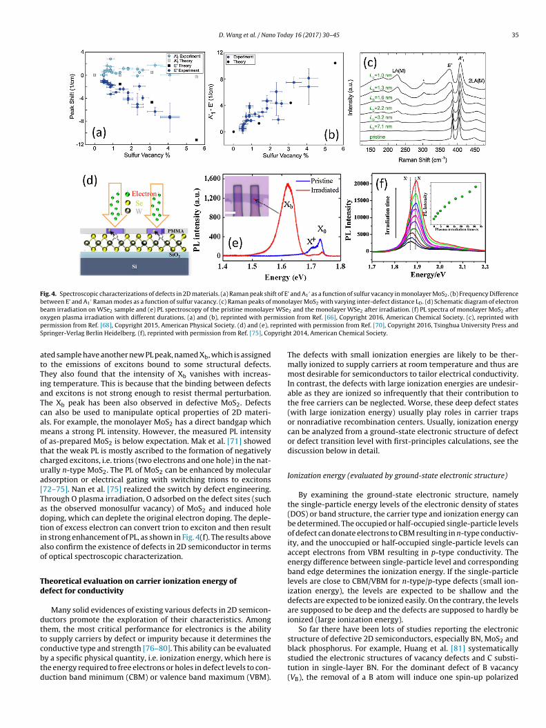
D. Wang et al. / Nano Today 16 (2017) 30–45 35
Fig. 4. Spectroscopic characterizations of defects in 2D materials. (a) Raman peak shift of E’ and A1′ as a function of sulfur vacancy in monolayer MoS2. (b) Frequency Difference
between E’ and A1′ Raman modes as a function of sulfur vacancy. (c) Raman peaks of monolayer MoS2 with varying inter-defect distance LD. (d) Schematic diagram of electron
beam irradiation on WSe2 sample and (e) PL spectroscopy of the pristine monolayer WSe2 and the monolayer WSe2 after irradiation. (f) PL spectra of monolayer MoS2 aftero missip eprinS pyrigh
atTiaTcamotcua[Tadtiao
Td
dttcbtd
xygen plasma irradiation with different durations. (a) and (b), reprinted with perermission from Ref. [68], Copyright 2015, American Physical Society. (d) and (e), rpringer-Verlag Berlin Heidelberg. (f), reprinted with permission from Ref. [75], Co
ted sample have another new PL peak, named Xb, which is assignedo the emissions of excitons bound to some structural defects.hey also found that the intensity of Xb vanishes with increas-ng temperature. This is because that the binding between defectsnd excitons is not strong enough to resist thermal perturbation.he Xb peak has been also observed in defective MoS2. Defectsan also be used to manipulate optical properties of 2D materi-ls. For example, the monolayer MoS2 has a direct bandgap whicheans a strong PL intensity. However, the measured PL intensity
f as-prepared MoS2 is below expectation. Mak et al. [71] showedhat the weak PL is mostly ascribed to the formation of negativelyharged excitons, i.e. trions (two electrons and one hole) in the nat-rally n-type MoS2. The PL of MoS2 can be enhanced by moleculardsorption or electrical gating with switching trions to excitons72–75]. Nan et al. [75] realized the switch by defect engineering.hrough O plasma irradiation, O adsorbed on the defect sites (suchs the observed monosulfur vacancy) of MoS2 and induced holeoping, which can deplete the original electron doping. The deple-ion of excess electron can convert trion to exciton and then resultn strong enhancement of PL, as shown in Fig. 4(f). The results abovelso confirm the existence of defects in 2D semiconductor in termsf optical spectroscopic characterization.
heoretical evaluation on carrier ionization energy ofefect for conductivity
Many solid evidences of existing various defects in 2D semicon-uctors promote the exploration of their characteristics. Amonghem, the most critical performance for electronics is the abilityo supply carriers by defect or impurity because it determines the
onductive type and strength [76–80]. This ability can be evaluatedy a specific physical quantity, i.e. ionization energy, which here ishe energy required to free electrons or holes in defect levels to con-uction band minimum (CBM) or valence band maximum (VBM).on from Ref. [66], Copyright 2016, American Chemical Society. (c), reprinted withted with permission from Ref. [70], Copyright 2016, Tsinghua University Press andt 2014, American Chemical Society.
The defects with small ionization energies are likely to be ther-mally ionized to supply carriers at room temperature and thus aremost desirable for semiconductors to tailor electrical conductivity.In contrast, the defects with large ionization energies are undesir-able as they are ionized so infrequently that their contribution tothe free carriers can be neglected. Worse, these deep defect states(with large ionization energy) usually play roles in carrier trapsor nonradiative recombination centers. Usually, ionization energycan be analyzed from a ground-state electronic structure of defector defect transition level with first-principles calculations, see thediscussion below in detail.
Ionization energy (evaluated by ground-state electronic structure)
By examining the ground-state electronic structure, namelythe single-particle energy levels of the electronic density of states(DOS) or band structure, the carrier type and ionization energy canbe determined. The occupied or half-occupied single-particle levelsof defect can donate electrons to CBM resulting in n-type conductiv-ity, and the unoccupied or half-occupied single-particle levels canaccept electrons from VBM resulting in p-type conductivity. Theenergy difference between single-particle level and correspondingband edge determines the ionization energy. If the single-particlelevels are close to CBM/VBM for n-type/p-type defects (small ion-ization energy), the levels are expected to be shallow and thedefects are expected to be ionized easily. On the contrary, the levelsare supposed to be deep and the defects are supposed to hardly beionized (large ionization energy).
So far there have been lots of studies reporting the electronicstructure of defective 2D semiconductors, especially BN, MoS2 and
black phosphorus. For example, Huang et al. [81] systematicallystudied the electronic structures of vacancy defects and C substi-tution in single-layer BN. For the dominant defect of B vacancy(VB), the removal of a B atom will induce one spin-up polarized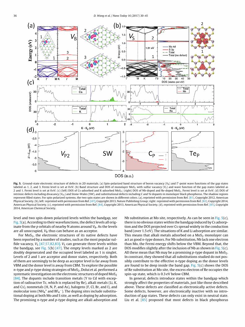
36 D. Wang et al. / Nano Today 16 (2017) 30–45
Fig. 5. Ground-state electronic structure of defects in 2D materials. (a) Spin-polarized band structure of boron vacancy (VB) and �-point wave functions of the gap stateslabeled as 1, 2, and 3. Fermi level is set at 0 eV. (b) Band structure and DOS of monolayer MoS2 with sulfur vacancy (VS) and wave function of the gap states labeled as2 and 1. Fermi level is set at 0 eV. (c) (left) DOS of Cs-adsorbed and K-adsorbed MoS2; (right) DOS of Nb-doped and Re-doped MoS2. Fermi level is set at 0 eV. (d) DOS ofintrinsic defects including divacancy (VP2) and Stone-Wales (SW), and substitutional defects including C and Te dopants in monolayer black phosphorus. The shadow regionsrepresent filled states. For spin-polarized systems, the two spin states are shown in different colors. (a), reprinted with permission from Ref. [81], Copyright 2012, AmericanP atureA 2013,
2
lFia
bfitdLoVns[tamtT
hysical Society. (b), left: reprinted with permission from Ref. [47], Copyright 2013, Nmerican Physical Society. (c), reprinted with permission from Ref. [84], Copyright
014, American Chemical Society.
evel and two spin-down polarized levels within the bandgap, seeig. 5(a). According to their wavefunctions, the defect levels all orig-nate from the p orbitals of nearby N atoms around VB. As the levelsre all unoccupied, VB thus can behave as an acceptor.
For MoS2, the electronic structures of its native defects haveeen reported by a number of studies, such as the most popular sul-de vacancy, VS [47,57,82,83]. VS can generate three levels withinhe bandgap, see Fig. 5(b) [47]. The empty levels marked as 2 areoubly degenerated and the occupied level labeled as 1 is singlet.evels of 2 and 1 are acceptor and donor states, respectively. Bothf them are seemingly to be deep as acceptor level is far away fromBM and the donor level is away from CBM. To explore the possible-type and p-type doing strategies of MoS2, Dolui et al. performed aystematic investigation on the electronic structures of doped MoS284]. The dopants include transition metals (Y to Cd with excep-ion of radioactive Tc, which is replaced by Re), alkali metals (Li, K,nd Cs), nonmetals (H, N, P, and As), halogens (F, Cl, Br, and I), and
olecular ions (NH4+ and BF4−). The doping sites include substitu-
ional doping at both Mo and S site, as well as doping by adsorption.he promising n-type and p-type doping are alkali adsorption and
Publishing Group; right: reprinted with permission from Ref. [82], Copyright 2014,American Physical Society. (d), reprinted with permission from Ref. [85], Copyright
Nb substitution at Mo site, respectively. As can be seen in Fig. 5(c),there is no obvious states within the bandgap induced by Cs adsorp-tion and the DOS projected over Cs spread widely in the conductionband (over 1.5 eV). The situations of K and Li adsorption are similar.This means that alkali metals adsorbed on a MoS2 monolayer canact as good n-type donors. For Nb substitution, Nb lack one electronthan Mo, the Fermi energy shifts below the VBM. Beyond that, theDOS modifies slightly after the inclusion of Nb as shown in Fig. 5(c).All these mean that Nb may be a promising p-type dopant in MoS2.In constrast, they showed that all substitutions studied do not pos-sibly contribute to the effective n-type doping as the donor levelsare found to be deep inside the band gap. Fig. 5(c) shows the DOSof Re substitution at Mo site, the excess electron of Re occupies thespin-up state, which is 0.3 eV below CBM.
In general, defects introduce states within the bandgap whichstrongly affect the properties of materials, just like those describedabove. These defects are classified as electronically active defects.
Some defects, however, are electronically inactive with no intro-duction of gap states. These defects can only exist in neutral state.Liu et al. [85] proposed that most defects in black phosphorus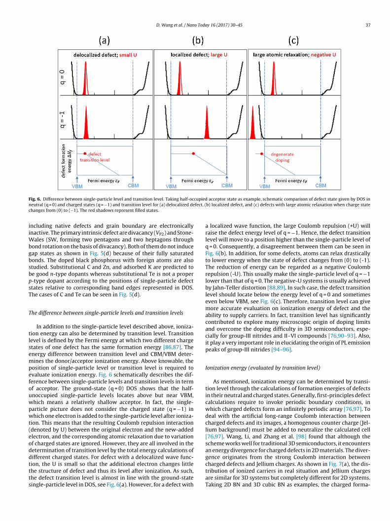
D. Wang et al. / Nano Today 16 (2017) 30–45 37
F cupiedn fect, (c
iiWbgbsbpsT
T
tlsempefouwpwt(eoddttts
ig. 6. Difference between single-particle level and transition level. Taking half-oceutral (q = 0) and charged states (q = −1) and transition level for (a) delocalized dehanges from (0) to (−1). The red shadows represent filled states.
ncluding native defects and grain boundary are electronicallynactive. The primary intrinsic defect are divacancy (VP2) and Stone-
ales (SW, forming two pentagons and two heptagons throughond rotation on the basis of divacancy). Both of them do not induceap states as shown in Fig. 5(d) because of their fully saturatedonds. The doped black phosphorus with foreign atoms are alsotudied. Substitutional C and Zn, and adsorbed K are predicted toe good n-type dopants whereas substitutional Te is not a proper-type dopant according to the positions of single-particle defecttates relative to corresponding band edges represented in DOS.he cases of C and Te can be seen in Fig. 5(d).
he difference between single-particle levels and transition levels
In addition to the single-particle level described above, ioniza-ion energy can also be determined by transition level. Transitionevel is defined by the Fermi energy at which two different chargetates of one defect has the same formation energy [86,87]. Thenergy difference between transition level and CBM/VBM deter-ines the donor/acceptor ionization energy. Above knowable, the
osition of single-particle level or transition level is required tovaluate ionization energy. Fig. 6 schematically describes the dif-erence between single-particle levels and transition levels in termf acceptor. The ground-state (q = 0) DOS shows that the half-noccupied single-particle levels locates above but near VBM,hich means a relatively shallow acceptor. In fact, the single-article picture does not consider the charged state (q = −1) inhich one electron is added to the single-particle level after ioniza-
ion. This means that the resulting Coulomb repulsion interactiondenoted by U) between the original electron and the new-addedlectron, and the corresponding atomic relaxation due to variationf charged states are ignored. However, they are all involved in theetermination of transition level by the total energy calculations ofifferent charged states. For defect with a delocalized wave func-
ion, the U is small so that the additional electron changes littlehe structure of defect and thus its level after ionization. As such,he defect transition level is almost in line with the ground-stateingle-particle level in DOS, see Fig. 6(a). However, for a defect withacceptor state as example, schematic comparison of defect state given by DOS inb) localized defect, and (c) defects with large atomic relaxation when charge state
a localized wave function, the large Coulomb repulsion (+U) willraise the defect energy level of q = −1. Hence, the defect transitionlevel will move to a position higher than the single-particle level ofq = 0. Consequently, a disagreement between them can be seen inFig. 6(b). In addition, for some defects, atoms can relax drasticallyto lower energy when the state of defect changes from (0) to (-1).The reduction of energy can be regarded as a negative Coulombrepulsion (-U). This usually make the single-particle level of q = −1lower than that of q = 0. The negative-U systems is usually achievedby Jahn-Teller distortion [88,89]. In such case, the defect transitionlevel should locate below the energy level of q = 0 and sometimeseven below VBM, see Fig. 6(c). Therefore, transition level can givemore accurate evaluation on ionization energy of defect and theability to supply carriers. In fact, transition level has significantlycontributed to explore many microscopic origin of doping limitsand overcome the doping difficulty in 3D semiconductors, espe-cially for group-III nitrides and II–VI compounds [76,90–93]. Also,it play a very important role in elucidating the origin of PL emissionpeaks of group-III nitrides [94–96].
Ionization energy (evaluated by transition level)
As mentioned, ionization energy can be determined by transi-tion level through the calculations of formation energies of defectsin their neutral and charged states. Generally, first-principles defectcalculations require to invoke periodic boundary conditions, inwhich charged defects form an infinitely periodic array [76,97]. Todeal with the artificial long-range Coulomb interaction betweencharged defects and its images, a homogenous counter charge (Jel-lium background) must be added to neutralize the calculated cell[76,97]. Wang, Li, and Zhang et al. [98] found that although thescheme works well for traditional 3D semiconductors, it encountersan energy divergence for charged defects in 2D materials. The diver-gence originates from the strong Coulomb interaction between
charged defects and Jellium charges. As shown in Fig. 7(a), the dis-tribution of ionized carriers in real situation and Jellium chargesare similar for 3D systems but completely different for 2D systems.Taking 2D BN and 3D cubic BN as examples, the charged forma-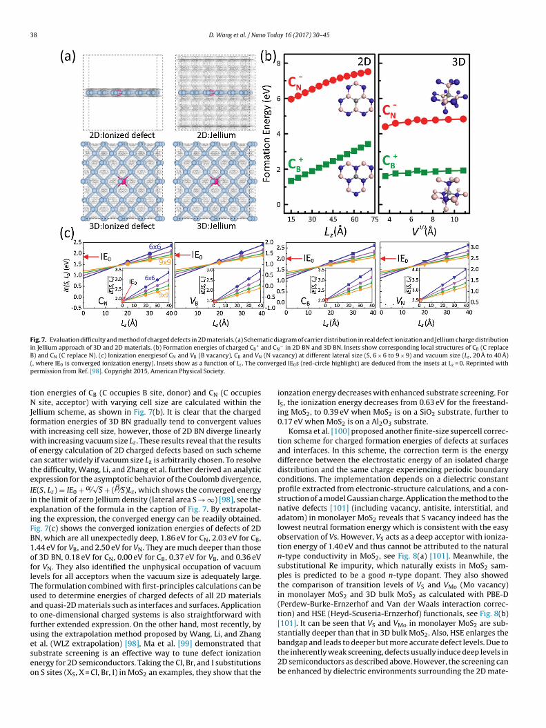
38 D. Wang et al. / Nano Today 16 (2017) 30–45
Fig. 7. Evaluation difficulty and method of charged defects in 2D materials. (a) Schematic diagram of carrier distribution in real defect ionization and Jellium charge distributionin Jellium approach of 3D and 2D materials. (b) Formation energies of charged CB
+ and CN− in 2D BN and 3D BN. Insets show corresponding local structures of CB (C replace
B (N va( nvergp
tNJfwwocteIieiFB1oflTuatfueseo
) and CN (C replace N). (c) Ionization energiesof CN and VB (B vacancy), CB and VN
, where IE0 is converged ionization energy). Insets show as a function of Lz . The coermission from Ref. [98]. Copyright 2015, American Physical Society.
ion energies of CB (C occupies B site, donor) and CN (C occupies site, acceptor) with varying cell size are calculated within the
ellium scheme, as shown in Fig. 7(b). It is clear that the chargedormation energies of 3D BN gradually tend to convergent valuesith increasing cell size, however, those of 2D BN diverge linearlyith increasing vacuum size Lz . These results reveal that the results
f energy calculation of 2D charged defects based on such schemean scatter widely if vacuum size Lz is arbitrarily chosen. To resolvehe difficulty, Wang, Li, and Zhang et al. further derived an analyticxpression for the asymptotic behavior of the Coulomb divergence,E(S, Lz) = IE0 + ˛⁄
√S + (ˇ⁄S)Lz , which shows the converged energy
n the limit of zero Jellium density (lateral area S → ∞) [98], see thexplanation of the formula in the caption of Fig. 7. By extrapolat-ng the expression, the converged energy can be readily obtained.ig. 7(c) shows the converged ionization energies of defects of 2DN, which are all unexpectedly deep, 1.86 eV for CN, 2.03 eV for CB,.44 eV for VB, and 2.50 eV for VN. They are much deeper than thosef 3D BN, 0.18 eV for CN, 0.00 eV for CB, 0.37 eV for VB, and 0.36 eVor VN. They also identified the unphysical occupation of vacuumevels for all acceptors when the vacuum size is adequately large.he formulation combined with first-principles calculations can besed to determine energies of charged defects of all 2D materialsnd quasi-2D materials such as interfaces and surfaces. Applicationo one-dimensional charged systems is also straightforward withurther extended expression. On the other hand, most recently, bysing the extrapolation method proposed by Wang, Li, and Zhang
t al. (WLZ extrapolation) [98], Ma et al. [99] demonstrated thatubstrate screening is an effective way to tune defect ionizationnergy for 2D semiconductors. Taking the Cl, Br, and I substitutionsn S sites (XS, X = Cl, Br, I) in MoS2 an examples, they show that thecancy) at different lateral size (S, 6 × 6 to 9 × 9) and vacuum size (Lz , 20 Å to 40 Å)ed IE0s (red-circle highlight) are deduced from the insets at Lz = 0. Reprinted with
ionzation energy decreases with enhanced substrate screening. ForIS, the ionization energy decreases from 0.63 eV for the freestand-ing MoS2, to 0.39 eV when MoS2 is on a SiO2 substrate, further to0.17 eV when MoS2 is on a Al2O3 substrate.
Komsa et al. [100] proposed another finite-size supercell correc-tion scheme for charged formation energies of defects at surfacesand interfaces. In this scheme, the correction term is the energydifference between the electrostatic energy of an isolated chargedistribution and the same charge experiencing periodic boundaryconditions. The implementation depends on a dielectric constantprofile extracted from electronic-structure calculations, and a con-struction of a model Gaussian charge. Application the method to thenative defects [101] (including vacancy, antisite, interstitial, andadatom) in monolayer MoS2 reveals that S vacancy indeed has thelowest neutral formation energy which is consistent with the easyobservation of Vs. However, VS acts as a deep acceptor with ioniza-tion energy of 1.40 eV and thus cannot be attributed to the naturaln-type conductivity in MoS2, see Fig. 8(a) [101]. Meanwhile, thesubstitutional Re impurity, which naturally exists in MoS2 sam-ples is predicted to be a good n-type dopant. They also showedthe comparison of transition levels of VS and VMo (Mo vacancy)in monolayer MoS2 and 3D bulk MoS2 as calculated with PBE-D(Perdew-Burke-Ernzerhof and Van der Waals interaction correc-tion) and HSE (Heyd-Scuseria-Ernzerhof) functionals, see Fig. 8(b)[101]. It can be seen that VS and VMo in monolayer MoS2 are sub-stantially deeper than that in 3D bulk MoS2. Also, HSE enlarges the
bandgap and leads to deeper but more accurate defect levels. Due tothe inherently weak screening, defects usually induce deep levels in2D semiconductors as described above. However, the screening canbe enhanced by dielectric environments surrounding the 2D mate-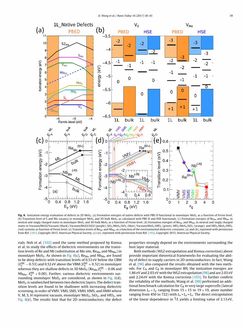
D. Wang et al. / Nano Today 16 (2017) 30–45 39
Fig. 8. Ionization energy evaluation of defects in 2D MoS2. (a) Formation energies of native defects with PBE-D functional in monolayer MoS2 as a function of Fermi level.(b) Transition level of S and Mo vacancy in monolayer MoS2 and 3D bulk MoS2 as calculated with PBE-D and HSE functionals. (c) Formation energies of ReMo and NbMo inneutral and singly charged states in monolayer MoS2 and 3D bulk MoS2 as a function of Fermi level. (d) Formation energies of ReMo and NbMo in neutral and singly chargeds iO2 (b( unctiof ermis
retmt(wNrMssVF
tates in Vacuum/MoS2/Vacuum (black), Vacuum/MoS2/SiO2 (purple), SiO2/MoS2/Sred) systems as function of Fermi level. (e) Transition levels of ReMo and NbMo as a from Ref. [101], Copyright 2015, American Physical Society. (c)-(e), reprinted with p
ials. Noh et al. [102] used the same method proposed by Komsat al. to study the effects of dielectric environments on the transi-ion levels of Re and Nb (substitution at Mo site, ReMo and NbMo) in
onolayer MoS2. As shown in Fig. 8(c), ReMo and NbMo are foundo be deep defects with transition levels of 0.53 eV below the CBMEML
C − 0.53) and 0.52 eV above the VBM (EMLV + 0.52) in monolayer
hereas they are shallow defects in 3D MoS2 (ReMo,EMLC − 0.06 and
bMo, EMLV + 0.00). Further, various dielectric environments sur-
ounding monolayer MoS2 are considered, as shown in Fig. 8(d).oS2 is sandwiched between two dielectric layers. The defect tran-
ition levels are found to be shallower with increasing dielectric
creening, in order of VMV, VMS, SMS, VMH, HMS, and HMH where, M, S, H represent vacuum, monolayer MoS2, SiO2, and HfO2, seeig. 8(e). The results hint that for 2D semiconductors, the defectlue), Vacuum/MoS2/HfO2 (green), HfO2/MoS2/SiO2 (orange), and HfO2/MoS2/HfO2
n of the environmental dielectric constants. (a) and (b), reprinted with permissionsion from Ref. [102], Copyright 2015, American Physical Society.
properties strongly depend on the environments surrounding thehost layer material.
Both methods (WLZ extrapolation and Komsa correction) aboveprovide important theoretical frameworks for evaluating the abil-ity of defect to supply carriers in 2D semiconductors. In fact, Wanget al. [98] also compared the results obtained with the two meth-ods. For CN and CB in monolayer BN, the ionization energies are1.86 eV and 2.03 eV with the WLZ extrapolation [98] and are 2.03 eVand 2.24 eV with the Komsa correction [103]. To further confirmthe reliability of the methods, Wang et al. [98] performed an addi-tional benchmark calculation for CB in very large supercells (lateral
dimension Lx × Ly ranging from 15 × 15 to 19 × 19, atom numberranging from 450 to 722) with Lx = Ly = Lz. The direct extrapolationof the linear dependence in 1⁄L yields a limiting value of 2.13 eV,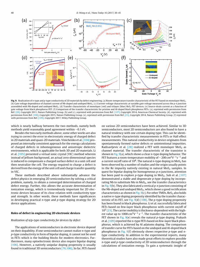
40 D. Wang et al. / Nano Today 16 (2017) 30–45
Fig. 9. Realization of n-type and p-type conductivity of 2D materials by defect engineering. (a) Room-temperature transfer characteristic of the FET based on monolayer MoS2.(b) Gate voltage dependence of channel current of Nb-doped and undoped MoS2. (c) Current-voltage characteristic at variable gate voltage measured across the p-n junctionassembled with Nb-doped and undoped MoS2. (d) Transfer characteristic of monolayer (red) and trilayer (blue) ReS2 FET devices. (e) Source-drain current as a function ofgate voltage from black phosphorus FET. (f) Comparison of the transfer characteristic for pristine and Al-doped black phosphorus FETs. (a), reprinted with permission fromR missiop withw
wm
tipoeeiitdi
dpditaid
R
R
opit[f
ef. [28], Copyright 2011, Nature Publishing Group. (b) and (c), reprinted with perermission from Ref. [108], Copyright 2015, Nature Publishing Group. (e), reprintedith permission from Ref. [109], Copyright 2017, Wiley Publishing Group.
hich is nearly halfway between the two methods, namely bothethods yield reasonably good agreement within ∼0.1 eV.Besides the two early methods above, some other works are also
rying to correct the error in electrostatic energy of charged defectn 2D materials and quasi-2D materials. Vinichenko et al. [104] pro-osed an internally consistent approach for the energy calculationsf charged defects in inhomogeneous and anisotropic dielectricnvironments, which is applicable for both 3D and 2D materials. Lit al. [105] presented a virtual ionic crystal (VIC) method whereinnstead of Jellium background, an actual zero-dimensional speciess induced to compensate a charged surface defect in a unit cell andhen neutralize the cell. The energy required to charge a defect iserived from the energy of the unit cell and charge transfer quantity
n VIC.These methods described above substantially advance the
efect physics in emerging 2D semiconductors by solving a criticalroblem, namely, to obtain a converged determination of chargedefect energy. Further, this allows the accurate determination of
onization energy, which is tremendously important for 2D elec-ronic devices because of its close relation with conductivity typend strength. In other words, these methods have significancesn developing practical n-type and p-type doping strategy for 2Device applications.
oles of defect in engineering 2D electronic devices
ealization of n/p-type conductivity for devices by defect
The applications of semiconductors in electronic device dependn their dopability. If one semiconductor cannot realize n-type and-type conductivity in form of bipolar doping, it cannot not be used
n FETs which is the building blocks for modern electronics. Fur-hermore, many optoelectronic device also require bipolar doping106]. However, a natively unipolar doping propensity is usuallyound in traditional 3D semiconductors [76,106]. So far, FETs basedn from Ref. [107], Copyright 2014, American Chemical Society. (d), reprinted with permission from Ref. [23], Copyright 2014, Nature Publishing Group. (f) reprinted
on various 2D semiconductors have been achieved. Similar to 3Dsemiconductors, most 2D semiconductors are also found to have anatural tendency with one certain doping type. This can be identi-fied by transfer characteristic measurements in FETs or Hall effectmeasurements. This natural conductivity in device originates fromspontaneously formed native defects or unintentional impurities.Radisavljevic et al. [28] realized a FET with monolayer MoS2 aschannel material. The transfer characteristic of the transistor isshown in Fig. 9(a), which shows a clear n-type doping behavior. TheFET features a room-temperature mobility of ∼ 200 cm2V−1s−1 anda current on/off ratio of 108. The natural n-type doping in MoS2 hasbeen observed by a number of studies and the origin usually pointsto the Re impurity natively existing in natural MoS2 samples. Inquest for bipolar doping for homogeneous p-n junctions, attentionhas been paid to explore p-type doping in MoS2. Suh et al. [107]demonstrated a stable and degenerate p-type doping by incorpo-rating Nb to substitute Mo in MoS2, see the transfer characteristicsin Fig. 9(b). They also fabricated a vertical p-n junction consisting ofthe Nb-doped and undoped MoS2, which shows a good rectificationcharacteristics as shown in Fig. 9(c). For other TMDs, ReS2 also holdsa native n-type doping propensity identified by the transfer charac-teristic of its FET, see Fig. 9(d) [108]. The p-type doping propensityhas been found in black phosphorus. Li et al. successfully fabricatedFETs based on few-layer black phosphorus with current on/off of105 [23]. The carrier mobility is thickness-dependent with the high-est value up to 1000 cm2V−1 s−1. The transfer characteristic of theFET shown in Fig. 9(e) reveals the natural p-type doping. Prakashet al. [109] reported the n-type FETs based on few-layer black phos-phorus, which is achieved by Al adatoms doping. The comparisonof transfer curve for FETs based on the undoped and Al-doped blackphosphorus in Fig. 9(f) obviously shows respective p-type and n-type conductivity. In addition to the experimental reports, many
theoretical studies have also made great efforts to explore possiblen-type and p-type conductivity of 2D semiconductors through thecalculations of ionization energy. To gain a systematic insight of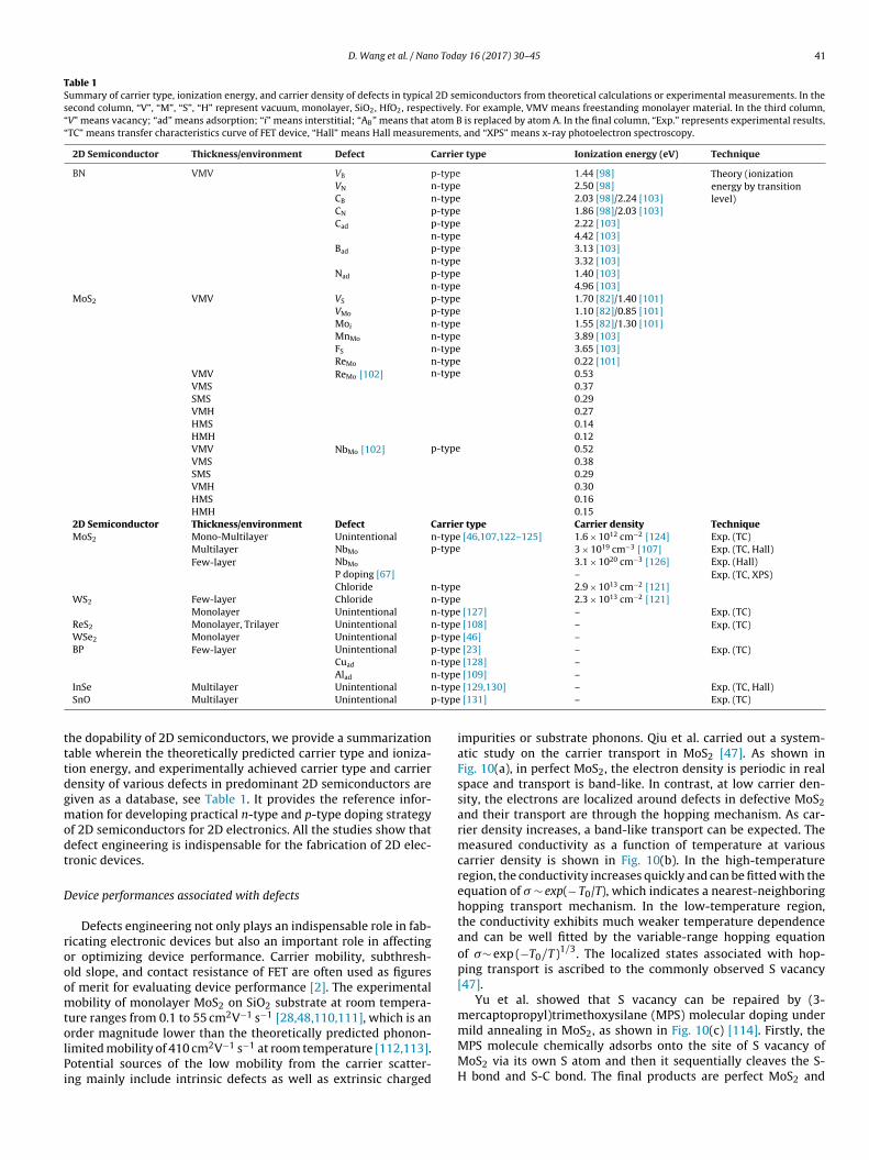
D. Wang et al. / Nano Today 16 (2017) 30–45 41
Table 1Summary of carrier type, ionization energy, and carrier density of defects in typical 2D semiconductors from theoretical calculations or experimental measurements. In thesecond column, “V”, “M”, “S”, “H” represent vacuum, monolayer, SiO2, HfO2, respectively. For example, VMV means freestanding monolayer material. In the third column,“V” means vacancy; “ad” means adsorption; “i” means interstitial; “AB” means that atom B is replaced by atom A. In the final column, “Exp.” represents experimental results,“TC” means transfer characteristics curve of FET device, “Hall” means Hall measurements, and “XPS” means x-ray photoelectron spectroscopy.
2D Semiconductor Thickness/environment Defect Carrier type Ionization energy (eV) Technique
BN VMV VB p-type 1.44 [98] Theory (ionizationenergy by transitionlevel)
VN n-type 2.50 [98]CB n-type 2.03 [98]/2.24 [103]CN p-type 1.86 [98]/2.03 [103]Cad p-type 2.22 [103]
n-type 4.42 [103]Bad p-type 3.13 [103]
n-type 3.32 [103]Nad p-type 1.40 [103]
n-type 4.96 [103]MoS2 VMV VS p-type 1.70 [82]/1.40 [101]
VMo p-type 1.10 [82]/0.85 [101]Moi n-type 1.55 [82]/1.30 [101]MnMo n-type 3.89 [103]FS n-type 3.65 [103]ReMo n-type 0.22 [101]
VMV ReMo [102] n-type 0.53VMS 0.37SMS 0.29VMH 0.27HMS 0.14HMH 0.12VMV NbMo [102] p-type 0.52VMS 0.38SMS 0.29VMH 0.30HMS 0.16HMH 0.15
2D Semiconductor Thickness/environment Defect Carrier type Carrier density TechniqueMoS2 Mono-Multilayer Unintentional n-type [46,107,122–125] 1.6 × 1012 cm−2 [124] Exp. (TC)
Multilayer NbMo p-type 3 × 1019 cm−3 [107] Exp. (TC, Hall)Few-layer NbMo 3.1 × 1020 cm−3 [126] Exp. (Hall)
P doping [67] – Exp. (TC, XPS)Chloride n-type 2.9 × 1013 cm−2 [121]
WS2 Few-layer Chloride n-type 2.3 × 1013 cm−2 [121]Monolayer Unintentional n-type [127] – Exp. (TC)
ReS2 Monolayer, Trilayer Unintentional n-type [108] – Exp. (TC)WSe2 Monolayer Unintentional p-type [46] –BP Few-layer Unintentional p-type [23] – Exp. (TC)
Cuad n-type [128] –-type-type-type
tttdgmodt
D
rooomtolPi
Alad nInSe Multilayer Unintentional nSnO Multilayer Unintentional p
he dopability of 2D semiconductors, we provide a summarizationable wherein the theoretically predicted carrier type and ioniza-ion energy, and experimentally achieved carrier type and carrierensity of various defects in predominant 2D semiconductors areiven as a database, see Table 1. It provides the reference infor-ation for developing practical n-type and p-type doping strategy
f 2D semiconductors for 2D electronics. All the studies show thatefect engineering is indispensable for the fabrication of 2D elec-ronic devices.
evice performances associated with defects
Defects engineering not only plays an indispensable role in fab-icating electronic devices but also an important role in affectingr optimizing device performance. Carrier mobility, subthresh-ld slope, and contact resistance of FET are often used as figuresf merit for evaluating device performance [2]. The experimentalobility of monolayer MoS2 on SiO2 substrate at room tempera-
ure ranges from 0.1 to 55 cm2V−1 s−1 [28,48,110,111], which is an
rder magnitude lower than the theoretically predicted phonon-imited mobility of 410 cm2V−1 s−1 at room temperature [112,113].otential sources of the low mobility from the carrier scatter-ng mainly include intrinsic defects as well as extrinsic charged[109] – [129,130] – Exp. (TC, Hall)
[131] – Exp. (TC)
impurities or substrate phonons. Qiu et al. carried out a system-atic study on the carrier transport in MoS2 [47]. As shown inFig. 10(a), in perfect MoS2, the electron density is periodic in realspace and transport is band-like. In contrast, at low carrier den-sity, the electrons are localized around defects in defective MoS2and their transport are through the hopping mechanism. As car-rier density increases, a band-like transport can be expected. Themeasured conductivity as a function of temperature at variouscarrier density is shown in Fig. 10(b). In the high-temperatureregion, the conductivity increases quickly and can be fitted with theequation of � ∼ exp(− T0/T), which indicates a nearest-neighboringhopping transport mechanism. In the low-temperature region,the conductivity exhibits much weaker temperature dependenceand can be well fitted by the variable-range hopping equationof �∼ exp (−T0/T)1/3. The localized states associated with hop-ping transport is ascribed to the commonly observed S vacancy[47].
Yu et al. showed that S vacancy can be repaired by (3-mercaptopropyl)trimethoxysilane (MPS) molecular doping under
mild annealing in MoS2, as shown in Fig. 10(c) [114]. Firstly, theMPS molecule chemically adsorbs onto the site of S vacancy ofMoS2 via its own S atom and then it sequentially cleaves the S-H bond and S-C bond. The final products are perfect MoS2 and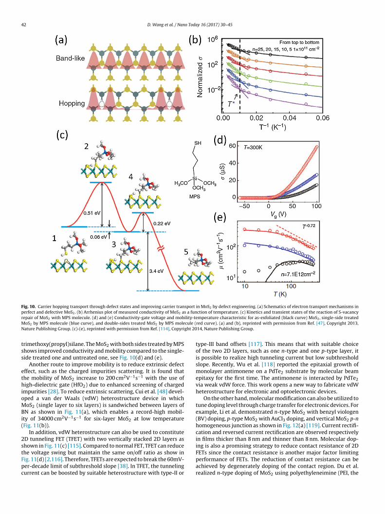
42 D. Wang et al. / Nano Today 16 (2017) 30–45
Fig. 10. Carrier hopping transport through defect states and improving carrier transport in MoS2 by defect engineering. (a) Schematics of electron transport mechanisms inperfect and defective MoS2. (b) Arrhenius plot of measured conductivity of MoS2 as a function of temperature. (c) Kinetics and transient states of the reaction of S-vacancyr ility-teM cule (N ght 20
tss
ethioMBi(
2stFpc
epair of MoS2 with MPS molecule. (d) and (e) Conductivity-gate voltage and moboS2 by MPS molecule (blue curve), and double-sides treated MoS2 by MPS moleature Publishing Group. (c)-(e), reprinted with permission from Ref. [114], Copyri
rimethoxy(propyl)silane. The MoS2 with both sides treated by MPShows improved conductivity and mobility compared to the single-ide treated one and untreated one, see Fig. 10(d) and (e).
Another route to improve mobility is to reduce extrinsic defectffect, such as the charged impurities scattering. It is found thathe mobility of MoS2 increase to 200 cm2V−1s−1 with the use ofigh-dielectric gate (HfO2) due to enhanced screening of charged
mpurities [28]. To reduce extrinsic scattering, Cui et al. [48] devel-ped a van der Waals (vdW) heterostructure device in whichoS2 (single layer to six layers) is sandwiched between layers of
N as shown in Fig. 11(a), which enables a record-high mobil-ty of 34000 cm2V−1s−1 for six-layer MoS2 at low temperatureFig. 11(b)).
In addition, vdW heterostructure can also be used to constituteD tunneling FET (TFET) with two vertically stacked 2D layers ashown in Fig. 11(c) [115]. Compared to normal FET, TFET can reducehe voltage swing but maintain the same on/off ratio as show in
ig. 11(d) [2,116]. Therefore, TFETs are expected to break the 60mV-er-decade limit of subthreshold slope [38]. In TFET, the tunnelingurrent can be boosted by suitable heterostructure with type-II ormperature characteristic for as-exfoliated (black curve) MoS2, single-side treatedred curve). (a) and (b), reprinted with permission from Ref. [47], Copyright 2013,14, Nature Publishing Group.
type-III band offsets [117]. This means that with suitable choiceof the two 2D layers, such as one n-type and one p-type layer, itis possible to realize high tunneling current but low subthresholdslope. Recently, Wu et al. [118] reported the epitaxial growth ofmonolayer antimonene on a PdTe2 substrate by molecular beamepitaxy for the first time. The antimonene is interacted by PdTe2via weak vdW force. This work opens a new way to fabricate vdWheterostructure for electronic and optoelectronic devices.
On the other hand, molecular modification can also be utilized totune doping level through charge transfer for electronic devices. Forexample, Li et al. demonstrated n-type MoS2 with benzyl viologen(BV) doping, p-type MoS2 with AuCl3 doping, and vertical MoS2 p-nhomogeneous junction as shown in Fig. 12(a) [119]. Current rectifi-cation and reversed current rectification are observed respectivelyin films thicker than 8 nm and thinner than 8 nm. Molecular dop-ing is also a promising strategy to reduce contact resistance of 2DFETs since the contact resistance is another major factor limiting
performance of FETs. The reduction of contact resistance can beachieved by degenerately doping of the contact region. Du et al.realized n-type doping of MoS2 using polyethyleneimine (PEI, the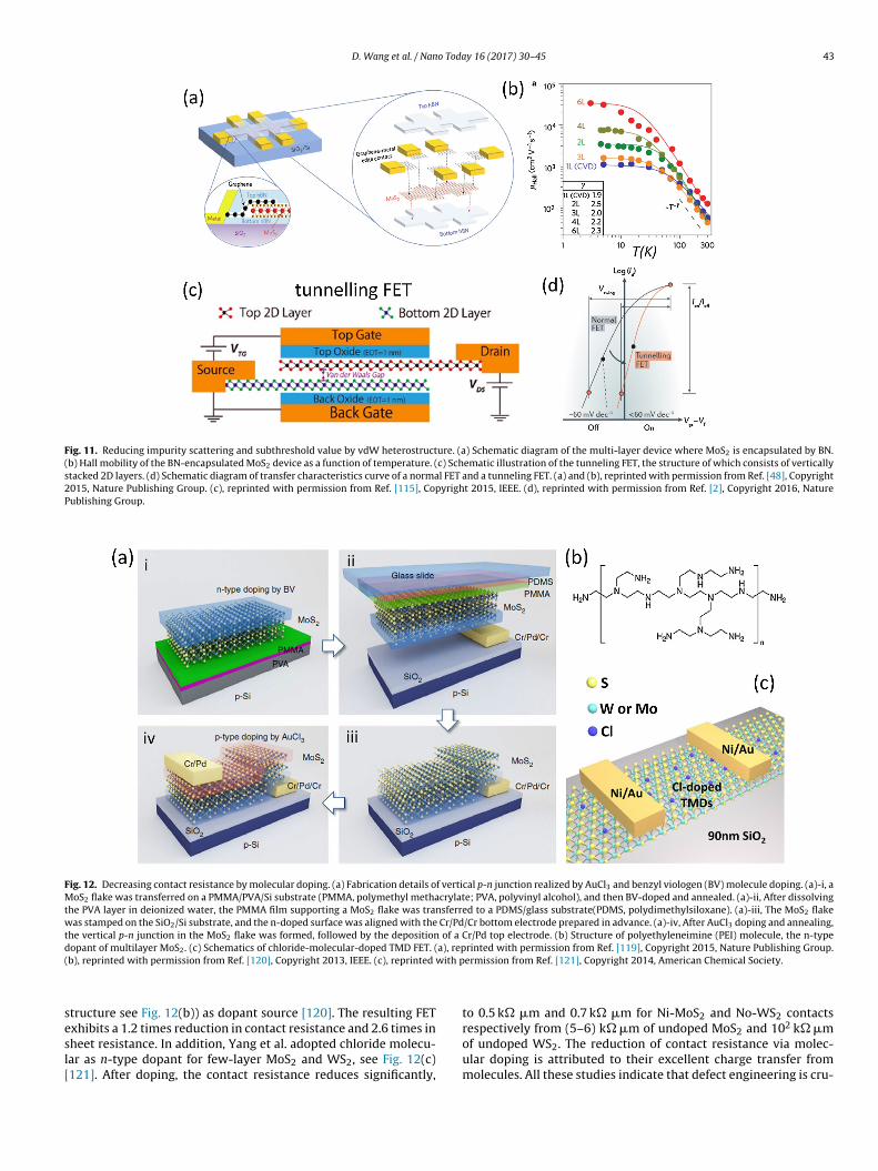
D. Wang et al. / Nano Today 16 (2017) 30–45 43
Fig. 11. Reducing impurity scattering and subthreshold value by vdW heterostructure. (a) Schematic diagram of the multi-layer device where MoS2 is encapsulated by BN.(b) Hall mobility of the BN-encapsulated MoS2 device as a function of temperature. (c) Schematic illustration of the tunneling FET, the structure of which consists of verticallystacked 2D layers. (d) Schematic diagram of transfer characteristics curve of a normal FET and a tunneling FET. (a) and (b), reprinted with permission from Ref. [48], Copyright2015, Nature Publishing Group. (c), reprinted with permission from Ref. [115], Copyright 2015, IEEE. (d), reprinted with permission from Ref. [2], Copyright 2016, NaturePublishing Group.
Fig. 12. Decreasing contact resistance by molecular doping. (a) Fabrication details of vertical p-n junction realized by AuCl3 and benzyl viologen (BV) molecule doping. (a)-i, aMoS2 flake was transferred on a PMMA/PVA/Si substrate (PMMA, polymethyl methacrylate; PVA, polyvinyl alcohol), and then BV-doped and annealed. (a)-ii, After dissolvingthe PVA layer in deionized water, the PMMA film supporting a MoS2 flake was transferred to a PDMS/glass substrate(PDMS, polydimethylsiloxane). (a)-iii, The MoS2 flakewas stamped on the SiO2/Si substrate, and the n-doped surface was aligned with the Cr/Pd/Cr bottom electrode prepared in advance. (a)-iv, After AuCl3 doping and annealing,the vertical p-n junction in the MoS2 flake was formed, followed by the deposition of a Cr/Pd top electrode. (b) Structure of polyethyleneimine (PEI) molecule, the n-typedopant of multilayer MoS . (c) Schematics of chloride-molecular-doped TMD FET. (a), reprinted with permission from Ref. [119], Copyright 2015, Nature Publishing Group.( with p
sesl[
2
b), reprinted with permission from Ref. [120], Copyright 2013, IEEE. (c), reprinted
tructure see Fig. 12(b)) as dopant source [120]. The resulting FET
xhibits a 1.2 times reduction in contact resistance and 2.6 times inheet resistance. In addition, Yang et al. adopted chloride molecu-ar as n-type dopant for few-layer MoS2 and WS2, see Fig. 12(c)121]. After doping, the contact resistance reduces significantly,ermission from Ref. [121], Copyright 2014, American Chemical Society.
to 0.5 k� �m and 0.7 k� �m for Ni-MoS2 and No-WS2 contactsrespectively from (5–6) k� �m of undoped MoS2 and 102 k� �m
of undoped WS2. The reduction of contact resistance via molec-ular doping is attributed to their excellent charge transfer frommolecules. All these studies indicate that defect engineering is cru-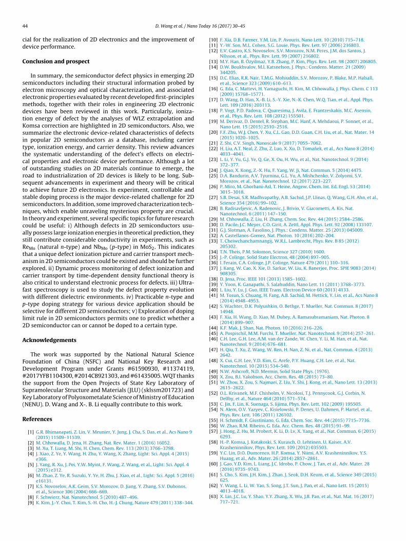
4 o Toda
cd
C
seemdtKsittcorstssnIcasRtaecafwpsl2
A
FD#tSK(
R
4 D. Wang et al. / Nan
ial for the realization of 2D electronics and the improvement ofevice performance.
onclusion and prospect
In summary, the semiconductor defect physics in emerging 2Demiconductors including their structural information probed bylectron microscopy and optical characterization, and associatedlectronic properties evaluated by recent developed first-principlesethods, together with their roles in engineering 2D electronic
evices have been reviewed in this work. Particularly, ioniza-ion energy of defect by the analyses of WLZ extrapolation andomsa correction are highlighted in 2D semiconductors. Also, weummarize the electronic device-related characteristics of defectsn popular 2D semiconductors as a database, including carrierype, ionization energy, and carrier density. This review advanceshe systematic understanding of the defect’s effects on electri-al properties and electronic device performance. Although a lotf outstanding studies on 2D materials continue to emerge, theoad to industrialization of 2D devices is likely to be long. Sub-equent advancements in experiment and theory will be criticalo achieve future 2D electronics. In experiment, controllable andtable doping process is the major device-related challenge for 2Demiconductors. In addition, some improved characterization tech-iques, which enable unraveling mysterious property are crucial.
n theory and experiment, several specific topics for future researchould be useful: i) Although defects in 2D semiconductors usu-lly possess large ionization energies in theoretical prediction, theytill contribute considerable conductivity in experiments, such aseMo (natural n-type) and NbMo (p-type) in MoS2. This indicateshat a unique defect ionization picture and carrier transport mech-nism in 2D semiconductors could be existed and should be furtherxplored. ii) Dynamic process monitoring of defect ionization andarrier transport by time-dependent density functional theory islso critical to understand electronic process for defects. iii) Ultra-ast spectroscopy is used to study the defect property evolutionith different dielectric environments. iv) Practicable n-type and
-type doping strategy for various device application should beelective for different 2D semiconductors; v) Exploration of dopingimit rule in 2D semiconductors permits one to predict whether aD semiconductor can or cannot be doped to a certain type.
cknowledgements
The work was supported by the National Natural Scienceoundation of China (NSFC) and National Key Research andevelopment Program under Grants #61590930, #11374119,2017YFB1104300, #2014CB921303, and #61435005. WQT thanks
he support from the Open Projects of State Key Laboratory ofupramolecular Structure and Materials (JLU) (sklssm201723) andey Laboratory of Polyoxometalate Science of Ministry of Education
NENU). D. Wang and X-. B. Li equally contribute to this work.
eferences
[1] G.R. Bhimanapati, Z. Lin, V. Meunier, Y. Jung, J. Cha, S. Das, et al., Acs Nano 9(2015) 11509–11539.
[2] M. Chhowalla, D. Jena, H. Zhang, Nat. Rev. Mater. 1 (2016) 16052.[3] M. Xu, T. Liang, M. Shi, H. Chen, Chem. Rev. 113 (2013) 3766–3798.[4] J. Xiao, Z. Ye, Y. Wang, H. Zhu, Y. Wang, X. Zhang, Light: Sci. Appl. 4 (2015)
e366.[5] J. Yang, R. Xu, J. Pei, Y.W. Myint, F. Wang, Z. Wang, et al., Light: Sci. Appl. 4
(2015) e312.[6] M. Zhao, Z. Ye, R. Suzuki, Y. Ye, H. Zhu, J. Xiao, et al., Light: Sci. Appl. 5 (2016)
e16131.[7] K.S. Novoselov, A.K. Geim, S.V. Morozov, D. Jiang, Y. Zhang, S.V. Dubonos,
et al., Science 306 (2004) 666–669.[8] F. Schwierz, Nat. Nanotechnol. 5 (2010) 487–496.[9] K. Kim, J.-Y. Choi, T. Kim, S.-H. Cho, H.-J. Chung, Nature 479 (2011) 338–344.
y 16 (2017) 30–45
[10] F. Xia, D.B. Farmer, Y.M. Lin, P. Avouris, Nano Lett. 10 (2010) 715–718.[11] Y.-W. Son, M.L. Cohen, S.G. Louie, Phys. Rev. Lett. 97 (2006) 216803.[12] E.V. Castro, K.S. Novoselov, S.V. Morozov, N.M. Peres, J.M. dos Santos, J.
Nilsson, et al., Phys. Rev. Lett. 99 (2007) 216802.[13] M.Y. Han, B. Özyilmaz, Y.B. Zhang, P. Kim, Phys. Rev. Lett. 98 (2007) 206805.[14] D.W. Boukhvalov, M.I. Katsnelson, J. Phys.: Condens. Matter. 21 (2009)
344205.[15] D.C. Elias, R.R. Nair, T.M.G. Mohiuddin, S.V. Morozov, P. Blake, M.P. Halsall,
et al., Science 323 (2009) 610–613.[16] G. Eda, C. Mattevi, H. Yamaguchi, H. Kim, M. Chhowalla, J. Phys. Chem. C 113
(2009) 15768–15771.[17] D. Wang, D. Han, X.-B. Li, S.-Y. Xie, N.-K. Chen, W.Q. Tian, et al., Appl. Phys.
Lett. 109 (2016) 203113.[18] P. Vogt, P.D. Padova, C. Quaresima, J. Avila, E. Frantzeskakis, M.C. Asensio,
et al., Phys. Rev. Lett. 108 (2012) 155501.[19] M. Derivaz, D. Dentel, R. Stephan, M.C. Hanf, A. Mehdaoui, P. Sonnet, et al.,
Nano Lett. 15 (2015) 2510–2516.[20] F.F. Zhu, W.J. Chen, Y. Xu, C.L. Gao, D.D. Guan, C.H. Liu, et al., Nat. Mater. 14
(2015) 1020–1025.[21] Z. Shi, C.V. Singh, Nanoscale 9 (2017) 7055–7062.[22] H. Liu, A.T. Neal, Z. Zhu, Z. Luo, X. Xu, D. Tomanek, et al., Acs Nano 8 (2014)
4033–4041.[23] L. Li, Y. Yu, G.J. Ye, Q. Ge, X. Ou, H. Wu, et al., Nat. Nanotechnol. 9 (2014)
372–377.[24] J. Qiao, X. Kong, Z.-X. Hu, F. Yang, W. Ji, Nat. Commun. 5 (2014) 4475.[25] D.A. Bandurin, A.V. Tyurnina, G.L. Yu, A. Mishchenko, V. Zolyomi, S.V.
Morozov, et al., Nat. Nanotechnol. 12 (2017) 223–227.[26] P. Miro, M. Ghorbani-Asl, T. Heine, Angew. Chem. Int. Ed. Engl. 53 (2014)
3015–3018.[27] S.B. Desai, S.R. Madhvapathy, A.B. Sachid, J.P. Llinas, Q. Wang, G.H. Ahn, et al.,
Science 354 (2016) 99–102.[28] B. Radisavljevic, A. Radenovic, J. Brivio, V. Giacometti, A. Kis, Nat.
Nanotechnol. 6 (2011) 147–150.[29] M. Chhowalla, Z. Liu, H. Zhang, Chem. Soc. Rev. 44 (2015) 2584–2586.[30] D. Pacile, J.C. Meyer, C.O. Girit, A. Zettl, Appl. Phys. Lett. 92 (2008) 133107.[31] G.J. Slotman, A. Fasolino, J. Phys.: Condens. Matter. 25 (2013) 045009.[32] A. Castellanos-Gomez, Nat. Photon. 10 (2016) 202–204.[33] T. Cheiwchanchamnangij, W.R.L. Lambrecht, Phys. Rev. B 85 (2012)
205302.[34] T.N. Theis, P.M. Solomon, Science 327 (2010) 1600.[35] J.-P. Colinge, Solid State Electron. 48 (2004) 897–905.[36] I. Ferain, C.A. Colinge, J.P. Colinge, Nature 479 (2011) 310–316.[37] J. Kang, W. Cao, X. Xie, D. Sarkar, W. Liu, K. Banerjee, Proc. SPIE 9083 (2014)
908305.[38] D. Jena, Proc. IEEE 101 (2013) 1585–1602.[39] Y. Yoon, K. Ganapathi, S. Salahuddin, Nano Lett. 11 (2011) 3768–3773.[40] L. Liu, Y. Lu, J. Guo, IEEE Trans. Electron Device 60 (2013) 4133.[41] M. Tosun, S. Chuang, H. Fang, A.B. Sachid, M. Hettick, Y. Lin, et al., Acs Nano 8
(2014) 4948–4953.[42] S. Wachter, D.K. Polyushkin, O. Bethge, T. Mueller, Nat. Commun. 8 (2017)
14948.[43] F. Xia, H. Wang, D. Xiao, M. Dubey, A. Ramasubramaniam, Nat. Photon. 8
(2014) 899–907.[44] K.F. Mak, J. Shan, Nat. Photon. 10 (2016) 216–226.[45] A. Pospischil, M.M. Furchi, T. Mueller, Nat. Nanotechnol. 9 (2014) 257–261.[46] C.H. Lee, G.H. Lee, A.M. van der Zande, W. Chen, Y. Li, M. Han, et al., Nat.
Nanotechnol. 9 (2014) 676–681.[47] H. Qiu, T. Xu, Z. Wang, W. Ren, H. Nan, Z. Ni, et al., Nat. Commun. 4 (2013)
2642.[48] X. Cui, G.H. Lee, Y.D. Kim, G. Arefe, P.Y. Huang, C.H. Lee, et al., Nat.
Nanotechnol. 10 (2015) 534–540.[49] N.W. Ashcroft, N.D. Mermin, Solid State Phys. (1976).[50] X. Zou, B.I. Yakobson, Acc. Chem. Res. 48 (2015) 73–80.[51] W. Zhou, X. Zou, S. Najmaei, Z. Liu, Y. Shi, J. Kong, et al., Nano Lett. 13 (2013)
2615–2622.[52] O.L. Krivanek, M.F. Chisholm, V. Nicolosi, T.J. Pennycook, G.J. Corbin, N.
Dellby, et al., Nature 464 (2010) 571–574.[53] C. Jin, F. Lin, K. Suenaga, S. Iijima, Phys. Rev. Lett. 102 (2009) 195505.[54] N. Alem, O.V. Yazyev, C. Kisielowski, P. Denes, U. Dahmen, P. Hartel, et al.,
Phys. Rev. Lett. 106 (2011) 126102.[55] H. Schmidt, F. Giustiniano, G. Eda, Chem. Soc. Rev. 44 (2015) 7715–7736.[56] W. Zhao, R.M. Ribeiro, G. Eda, Acc. Chem. Res. 48 (2015) 91–99.[57] J. Hong, Z. Hu, M. Probert, K. Li, D. Lv, X. Yang, et al., Nat. Commun. 6 (2015)
6293.[58] H.-P. Komsa, J. Kotakoski, S. Kurasch, O. Lehtinen, U. Kaiser, A.V.
Krasheninnikov, Phys. Rev. Lett. 109 (2012) 035503.[59] Y.C. Lin, D.O. Dumcenco, H.P. Komsa, Y. Niimi, A.V. Krasheninnikov, Y.S.
Huang, et al., Adv. Mater. 26 (2014) 2857–2861.[60] J. Gao, Y.D. Kim, L. Liang, J.C. Idrobo, P. Chow, J. Tan, et al., Adv. Mater. 28
(2016) 9735–9743.[61] S. Cho, S. Kim, J.H. Kim, J. Zhao, J. Seok, D.H. Keum, et al., Science 349 (2015)
625.[62] Y. Wang, L. Li, W. Yao, S. Song, J.T. Sun, J. Pan, et al., Nano Lett. 15 (2015)
4013–4018.[63] X. Lin, J.C. Lu, Y. Shao, Y.Y. Zhang, X. Wu, J.B. Pan, et al., Nat. Mat. 16 (2017)
717–721.
o Toda
Nano Lett. 16 (2016) 2145–2151.[129] W. Feng, W. Zheng, W. Cao, P. Hu, Adv. Mater. 26 (2014) 6587–6593.[130] S. Sucharitakul, N.J. Goble, U.R. Kumar, R. Sankar, Z.A. Bogorad, F.C. Chou,
et al., Nano Lett. 15 (2015) 3815–3819.
D. Wang et al. / Nan
[64] Z. Wu, Z. Ni, Nanophotonics (2017).[65] A. Eckmann, A. Felten, A. Mishchenko, L. Britnell, R. Krupke, K.S. Novoselov,
et al., Nano Lett. 12 (2012) 3925–3930.[66] W.M. Parkin, A. Balan, L. Liang, P.M. Das, M. Lamparski, C.H. Naylor, et al.,
Acs Nano 10 (2016) 4134–4142.[67] A. Nipane, D. Karmakar, N. Kaushik, S. Karande, S. Lodha, Acs Nano 10 (2016)
2128–2137.[68] S. Mignuzzi, A.J. Pollard, N. Bonini, B. Brennan, I.S. Gilmore, M.A. Pimenta,
et al., Phys. Rev. B 91 (2015) 195411.[69] E.D. Corro, H. Terrones, A. Elias, C. Fantini, S. Feng, M.A. Nguyen, et al., Acs
Nano 8 (2014) 9629.[70] Z. Wu, Z. Luo, Y. Shen, W. Zhao, W. Wang, H. Nan, et al., Nano Res. 9 (2016)
3622–3631.[71] K.F. Mak, K. He, C. Lee, G.H. Lee, J. Hone, T.F. Heinz, et al., Nat. Mater. 12
(2013) 207–211.[72] S. Mouri, Y. Miyauchi, K. Matsuda, Nano Lett. 13 (2013) 5944–5948.[73] A.K.M. Newaz, D. Prasai, J.I. Ziegler, D. Caudel, S. Robinson, R.F. Haglund Jr.,
et al., Solid State Commun. 155 (2013) 49–52.[74] S. Tongay, J. Zhou, C. Ataca, J. Liu, J.S. Kang, T.S. Matthews, et al., Nano Lett.
13 (2013) 2831–2836.[75] H. Nan, Z. Wang, W. Wang, Z. Liang, Y. Lu, Q. Chen, et al., Acs Nano 8 (2014)
5738.[76] S.B. Zhang, J. Phys. Condens. Matter 14 (2002) 881–903.[77] J. Chocholousová, V. Spirko, P. Hobza, Phys. Chem. Chem. Phys. 6 (2004)
37–41.[78] C.G. Van de Walle, J. Appl. Phys. 95 (2004) 3851.[79] A. Alkauskas, M.D. McCluskey, C.G. Van de Walle, J. Appl. Phys. 119 (2016)
181101.[80] C. Freysoldt, B. Grabowski, T. Hickel, J. Neugebauer, G. Kresse, A. Janotti,
et al., Rev. Mod. Phys. 86 (2014) 253–305.[81] B. Huang, H. Lee, Phys. Rev. B 86 (2012) 245406.[82] J.-Y. Noh, H. Kim, Y.-S. Kim, Phys. Rev. B 89 (2014) 205417.[83] C.S. K, R.C. Longo, R. Addou, R.M. Wallace, K. Cho, Nanotechnology 25 (2014)
375703.[84] K. Dolui, I. Rungger, C. Das Pemmaraju, S. Sanvito, Phys. Rev. B 88 (2013)
075420.[85] Y. Liu, F. Xu, Z. Zhang, E.S. Penev, B.I. Yakobson, Nano Lett. 14 (2014)
6782–6786.[86] S.B. Zhang, J.E. Northrup, Phys. Rev. Lett. 67 (1991) 2339–2342.[87] D. Han, D. West, X.-B. Li, S.-Y. Xie, H.-B. Sun, S.B. Zhang, Phys. Rev. B 82
(2010) 155132.[88] T. Yamabe, K. Yoshizawa, Y. Matsuura, K. Tanaka, Synth. Met. 75 (1995)
55–60.[89] F. Bechstedt, A. Zywietz, J. Furthmuller, Europhys. Lett. 44 (1998) 309–314.[90] S.B. Zhang, S.H. Wei, A. Zunger, Phys. Rev. B 63 (2001) 075205.[91] C.H. Park, S.B. Zhang, S.-H. Wei, Phys. Rev. B 66 (2002) 073202.[92] J.L. Lyons, A. Janotti, C.G. Van de Walle, Appl. Phys. Lett. 95 (2009) 252105.[93] S.J. Pearton, F. Ren, A.P. Zhang, K.P. Lee, Mater. Sci. Eng. R 30 (2000) 55–212.[94] J.L. Lyons, A. Janotti, C.G. Van de Walle, Phys. Rev. Lett. 108 (2012) 156403.[95] S.G. Christenson, W. Xie, Y.Y. Sun, S.B. Zhang, J. Appl. Phys. 118 (2015)
135708.
[96] J.L. Lyons, A. Janotti, C.G. Van de Walle, Appl. Phys. Lett. 97 (2010) 152108.[97] J. Lento, J.-L. Mozos, R.M. Nieminen, J. Phys. Condens. Matter 14 (2002)2637–2645.[98] D. Wang, D. Han, X.-B. Li, S.-Y. Xie, N.-K. Chen, W.Q. Tian, et al., Phys. Rev.
Lett. 114 (2015) 196801.
y 16 (2017) 30–45 45
[99] J. Ma, Z.G. Yu, Y.-W. Zhang, Phys. Rev. B 95 (2017) 165447.[100] H.-P. Komsa, A. Pasquarello, Phys. Rev. Lett. 110 (2013) 095505.[101] H.-P. Komsa, A.V. Krasheninnikov, Phys. Rev. B 91 (2015) 125304.[102] J.-Y. Noh, H. Kim, M. Park, Y.-S. Kim, Phys. Rev. B 92 (2015) 115431.[103] H.-P. Komsa, N. Berseneva, A.V. Krasheninnikov, R.M. Nieminen, Phys. Rev. X
4 (2014) 031044.[104] D. Vinichenko, M.G. Sensoy, C.M. Friend, E. Kaxiras, arXiv (2017),
1701.02521v1.[105] F. Li, Z. Hu, Z. Niu, L. Zhang, arXiv (2016), 1606.04185.[106] S.-H. Wei, Comput. Mater. Sci. 30 (2004) 337–348.[107] J. Suh, T.E. Park, D.Y. Lin, D. Fu, J. Park, H.J. Jung, et al., Nano Lett. 14 (2014)
6976–6982.[108] E. Liu, Y. Fu, Y. Wang, Y. Feng, H. Liu, X. Wan, et al., Nat. Commun. 6 (2015)
6991.[109] A. Prakash, Y. Cai, G. Zhang, Y.W. Zhang, K.W. Ang, Small 13 (2017) 1602909.[110] K.S. Novoselov, D. Jiang, F. Schedin, T.J. Booth, V.V. Khotkevich, S.V. Morozov,
et al., Proc. Natl. Acad. Sci. 102 (2005) 10451–10453.[111] R. Kappera, D. Voiry, S.E. Yalcin, W. Jen, M. Acerce, S. Torrel, et al., APL Mater.
2 (2014) 092516.[112] K. Kaasbjerg, K.S. Thygesen, K.W. Jacobsen, Phys. Rev. B 85 (2012) 115317.[113] T. Gunst, T. Markussen, K. Stokbro, M. Brandbyge, Phys. Rev. B 93 (2016)
035414.[114] Z. Yu, Y. Pan, Y. Shen, Z. Wang, Z.Y. Ong, T. Xu, et al., Nat. Commun. 5 (2014)
5290.[115] M. Li, D. Esseni, J.J. Nahas, D. Jena, H.G. Xing, IEEE J. Electron Device Soc. 3
(2015) 200–207.[116] Z. Qin, Z. Wei, A. Seabaugh, IEEE Electron Device Lett. 27 (2006) 297–300.[117] G. Zhou, R. Li, M. Vasen, S. Chae, Y. Lu, et al., IEEE Int. Electron Devices Meet.
(2012), 32.6.1–32.6.4.[118] X. Wu, Y. Shao, H. Liu, Z. Feng, Y.L. Wang, J.T. Sun, et al., Adv. Mater. 29
(2017).[119] H.M. Li, D. Lee, D. Qu, X. Liu, J. Ryu, A. Seabaugh, et al., Nat. Commun. 6
(2015) 6564.[120] Y. Du, H. Liu, A.T. Neal, M. Si, P.D. Ye, IEEE Electron Device Lett. 34 (2013)
1328–1330.[121] L. Yang, K. Majumdar, H. Liu, Y. Du, H. Wu, M. Hatzistergos, et al., Nano Lett.
14 (2014) 6275–6280.[122] H. Li, Z. Yin, Q. He, H. Li, X. Huang, G. Lu, et al., Small 8 (2012) 63–67.[123] H. Li, G. Lu, Z. Yin, Q. He, H. Li, Q. Zhang, et al., Small 8 (2012) 682–686.[124] S. Kim, A. Konar, W.S. Hwang, J.H. Lee, J. Lee, J. Yang, et al., Nat. Commun. 3
(2012) 1011.[125] B. Radisavljevic, M.B. Whitwick, A. Kis, Acs Nano 12 (2011) 9934–9938.[126] M.R. Laskar, D.N. Nath, L. Ma, E.W. Lee II, C.H. Lee, T. Kent, et al., Appl. Phys.
Lett. 104 (2014) 092104.[127] M.W. Iqbal, M.Z. Iqbal, M.F. Khan, M.A. Shehzad, Y. Seo, J.H. Park, et al., Sci.
Rep. 5 (2015) 10699.[128] S.P. Koenig, R.A. Doganov, L. Seixas, A. Carvalho, J.Y. Tan, K. Watanabe, et al.,
[131] K.J. Saji, K. Tian, M. Snure, A. Tiwari, Adv. Electron. Mater. 2 (2016) 1500453.