enhanced modeling methodology for system-level
TRANSCRIPT

ENHANCED MODELING METHODOLOGY FOR SYSTEM-LEVEL
ELECTROSTATIC DISCHARGE SIMULATION
BY
JIE XIONG
THESIS
Submitted in partial fulfillment of the requirements
for the degree of Master of Science in Electrical and Computer Engineering
in the Graduate College of the
University of Illinois at Urbana-Champaign, 2019
Urbana, Illinois
Adviser:
Professor Elyse Rosenbaum

ii
ABSTRACT
To enable accurate system-level electrostatic discharge (ESD) simulation, models for the
equipment under test, the ESD source, and the environment are required. This work presents
advanced modeling methods for the ESD source, the victim IC, and other on-board components,
most notably the transient voltage suppressor. Kernel regression is used to generate an enhanced
quasistatic I-V model of an IC pin, which reflects its dependency on the circuit board’s power
delivery network. S-parameter measurements enable the development of a model for an IEC
61000-4-2 ESD source that comprehends the coupling among the ground straps and the ground
plane. The transient-voltage-suppressor device is modeled using a behavioral snapback model
that shows better convergence in circuit simulation than piece-wise models. Furthermore, ESD-
induced soft failures are often caused by the noise coupled between the IC package traces. To
help identify this type of failure, a hybrid electromagnetic and circuit simulation approach is
demonstrated.

iii
ACKNOWLEDGMENTS
I would like to thank my adviser, Professor Rosenbaum. My research would have been
impossible without her guidance and support.
I would also like to thank many previous and current students for their invaluable help
with this work. They are Nicholas Thomson, Yang Xiu, Zaichen Chen, Collin Reiman and
Sandeep Vora.

iv
TABLE OF CONTENTS
CHAPTER 1: INTRODUCTION ................................................................................................... 1
1.1 Motivation ..................................................................................................................... 1
1.2 Thesis Overview ............................................................................................................ 2
CHAPTER 2: PDN-AWARE QUASISTATIC I-V MODELS ...................................................... 3
2.1 Conventional Quasistatic I-V Model ............................................................................. 3
2.2 Board PDN Representation ........................................................................................... 4
2.3 Kernel Regression .......................................................................................................... 6
2.4 Model Reduction ......................................................................................................... 10
CHAPTER 3: IMPROVED IEC 61000-4-2 ESD SOURCE MODEL ......................................... 13
3.1 IEC 61000-4-2 Test Setup ........................................................................................... 13
3.2 Deficiency of the Lumped RLC Model ....................................................................... 14
3.3 Model Enhancement with S-Parameters ...................................................................... 16
CHAPTER 4: PRACTICAL SYSTEM MODELING APPROACH ........................................... 19
4.1 Overview of the Test System ....................................................................................... 19
4.2 IC Signal Pin Model .................................................................................................... 21
4.3 Transient-voltage-suppression Diode Model ............................................................... 23
4.4 System Simulation Results .......................................................................................... 26
CHAPTER 5: ESD NOISE COUPLING ANALYSIS ................................................................. 30
CHAPTER 6: CONCLUSION ..................................................................................................... 34
REFERENCES ............................................................................................................................. 35
1
CHAPTER 1: INTRODUCTION
1.1 Motivation
Electrostatic discharge (ESD) is a high-current transient event that may result from
human or automated handling; it is ubiquitous during the manufacturing and assembly of
microelectronic components and systems. ESD can be destructive to semiconductor devices: The
high current densities in nanoscale devices may lead to thermal damage; furthermore, the
current-induced electric fields can cause dielectric breakdown.
The significance of system-level ESD reliability has led to concerted efforts by
manufacturers and researchers. A system is comprised of multiple components that interact with
each other. The Industry Council on ESD Target Levels advocates using SPICE-like circuit
simulation to evaluate system-level ESD reliability, rather than first identifying problems at the
time of product qualification testing. This paradigm was named system-efficient ESD design, or
SEED. From the description of SEED provided in [1], circuit simulation is used to obtain the
current and voltage waveforms at the “external pins” of any components that lie on the discharge
path. One-port models that have been optimized for high-current ESD-like conditions are used to
represent those external pins, and the reference terminal is connected to the system ground.
The SEED methodology has been applied in numerous case studies, e.g. [2], [3], [4]. In
most prior works, the integrated circuit (IC) components of the system are characterized using
transmission line pulse testing, and piecewise linear or other static models are used to represent
the I-V characteristic. However, a static model does not always yield accurate simulation results
[5]. The pulsed I-V characteristic measured at a signal pin of an IC is not independent of the
power delivery network (PDN) on the circuit board [6]; therefore, using a single I-V
characteristic to represent an IC introduces some inaccuracy into the simulation. Furthermore,
the conventional ESD source model lacks information about the coupling effect among the
ground straps and the metal planes in the system. Finally, SEED methodology only simulates the
primary current path. While it may be well suited to determine whether an IC will stay within its
2
safe operation area (SOA) during a system-level ESD event, it is not designed to identify ESD
noise hazards in a design; such noise has been associated with soft failures.
1.2 Thesis Overview
This work seeks to identify models for the IC and the system ESD current source that
yield more accurate results in a conventional system-level ESD simulation (i.e., SEED), and
simulation approaches that enable ESD-induced noise coupling analysis.
Chapter 2 presents a PDN-aware quasistatic I-V model for IC signal pins that is obtained
using kernel regression. In Chapter 3, an improved model for the IEC 61000-4-2 ESD generator,
also referred to as the ESD gun, that can comprehend the coupling effect of the metal straps and
planes associated with the system is presented and discussed. In Chapter 4, a practical example is
given to demonstrate the system modeling methodology with the enhanced models. Chapter 5
describes a technique to simulate the ESD-induced noise in the IC package.
3
CHAPTER 2: PDN-AWARE QUASISTATIC I-V MODELS
2.1 Conventional Quasistatic I-V Model
A transmission line pulse (TLP) tester generates a square-like current pulse by charging
up a 50 Ω open-ended transmission line and releasing the charge to the device under test (DUT).
The pulse width equals twice the propagation delay of the transmission line; the rise time can be
adjusted by a rise time filter. A typical TLP test uses 100 ns wide pulses with 10 ns rise time, as
it roughly emulates a human-body-model pulse. During the test, the current through and the
voltage across the DUT are measured simultaneously.
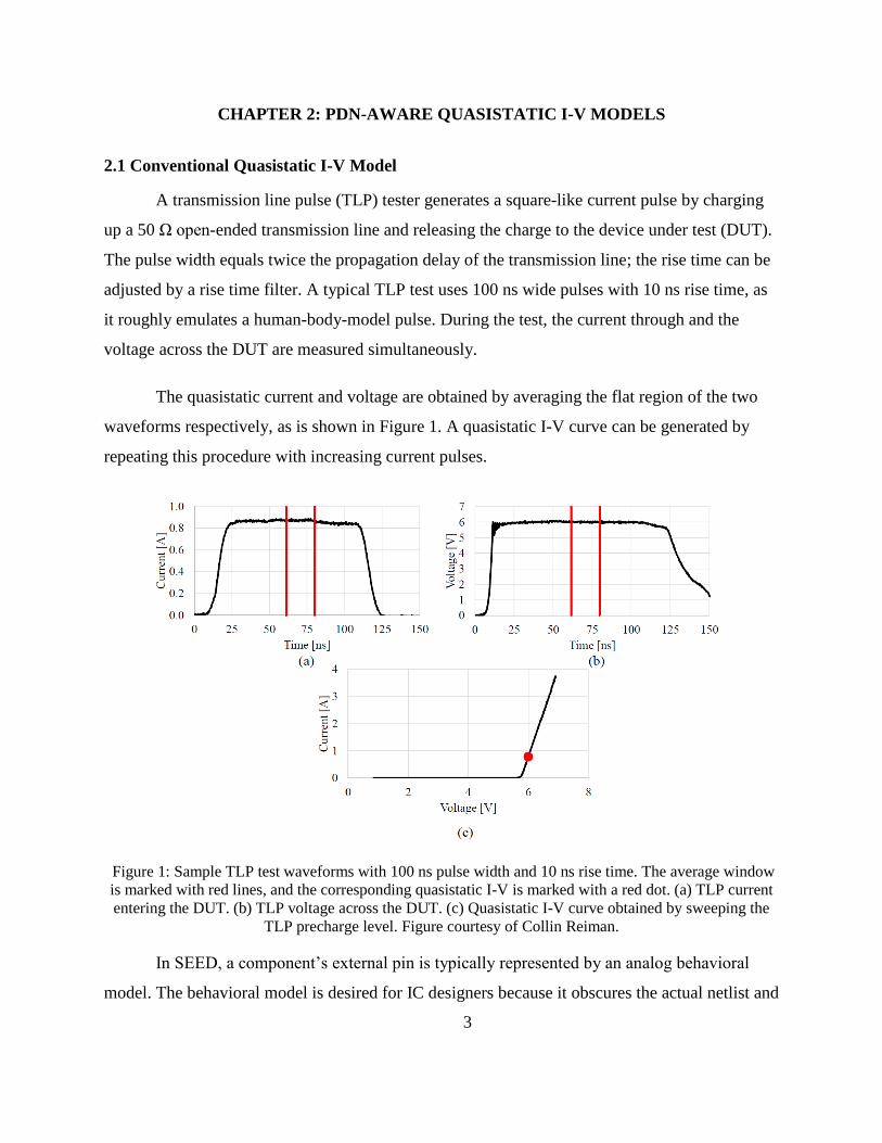
The quasistatic current and voltage are obtained by averaging the flat region of the two
waveforms respectively, as is shown in Figure 1. A quasistatic I-V curve can be generated by
repeating this procedure with increasing current pulses.
Figure 1: Sample TLP test waveforms with 100 ns pulse width and 10 ns rise time. The average window
is marked with red lines, and the corresponding quasistatic I-V is marked with a red dot. (a) TLP current
entering the DUT. (b) TLP voltage across the DUT. (c) Quasistatic I-V curve obtained by sweeping the
TLP precharge level. Figure courtesy of Collin Reiman.
In SEED, a component’s external pin is typically represented by an analog behavioral
model. The behavioral model is desired for IC designers because it obscures the actual netlist and
4
protects intellectual property. For users, often times, a behavioral model of the IC that is valid at
high current levels may not be provided, so obtaining a behavioral model from measurement data
becomes more important. A common way to construct the pin model is to fit a user-defined
function, e.g., a piecewise linear function, to the quasistatic I-V curve obtained from the TLP
measurements. It is customary to use the I-V model measured using one test board to represent
the same IC mounted on a different board, because we assume that the quasistatic behavior of the
IC is independent of the test board, although this is not always the case as will be discussed in
the next section. The model equations are usually written such that voltage is the independent
variable and current is a function of the voltage, except in cases where it is more convenient to
express voltage as a function of current. In principle, a wider variety of inputs may be used to
capture the circuit board dependency.
2.2 Board PDN Representation
A common system-level ESD test scenario involves discharge to a board trace directly
connected to an IO pin of a component. The discharge current enters the chip through the IO pin
and returns to ground through the board power delivery network (PDN). The board PDN
includes the supply planes, decoupling capacitors, and associated parasitics. Different PDN
designs result in different impedances on the current return paths. In a prior work [6], it was
observed that the quasistatic I-V characteristic measured at an IO pin is a function of the amount
and placement of the on-board decoupling capacitors; this finding is unsurprising because the
impedance of the current return path is strongly dependent on the decoupling capacitance. To
capture the effect of the board PDN in a one-port IO pin model, the PDN impedance needs to be
parameterized so that the I-V characteristic may be represented as a function of those parameters.
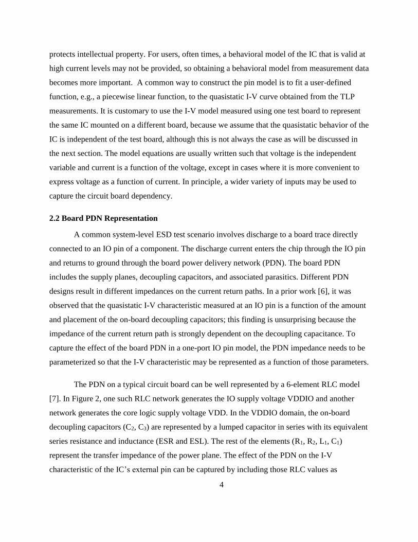
The PDN on a typical circuit board can be well represented by a 6-element RLC model
[7]. In Figure 2, one such RLC network generates the IO supply voltage VDDIO and another
network generates the core logic supply voltage VDD. In the VDDIO domain, the on-board
decoupling capacitors (C2, C3) are represented by a lumped capacitor in series with its equivalent
series resistance and inductance (ESR and ESL). The rest of the elements (R1, R2, L1, C1)
represent the transfer impedance of the power plane. The effect of the PDN on the I-V
characteristic of the IC’s external pin can be captured by including those RLC values as
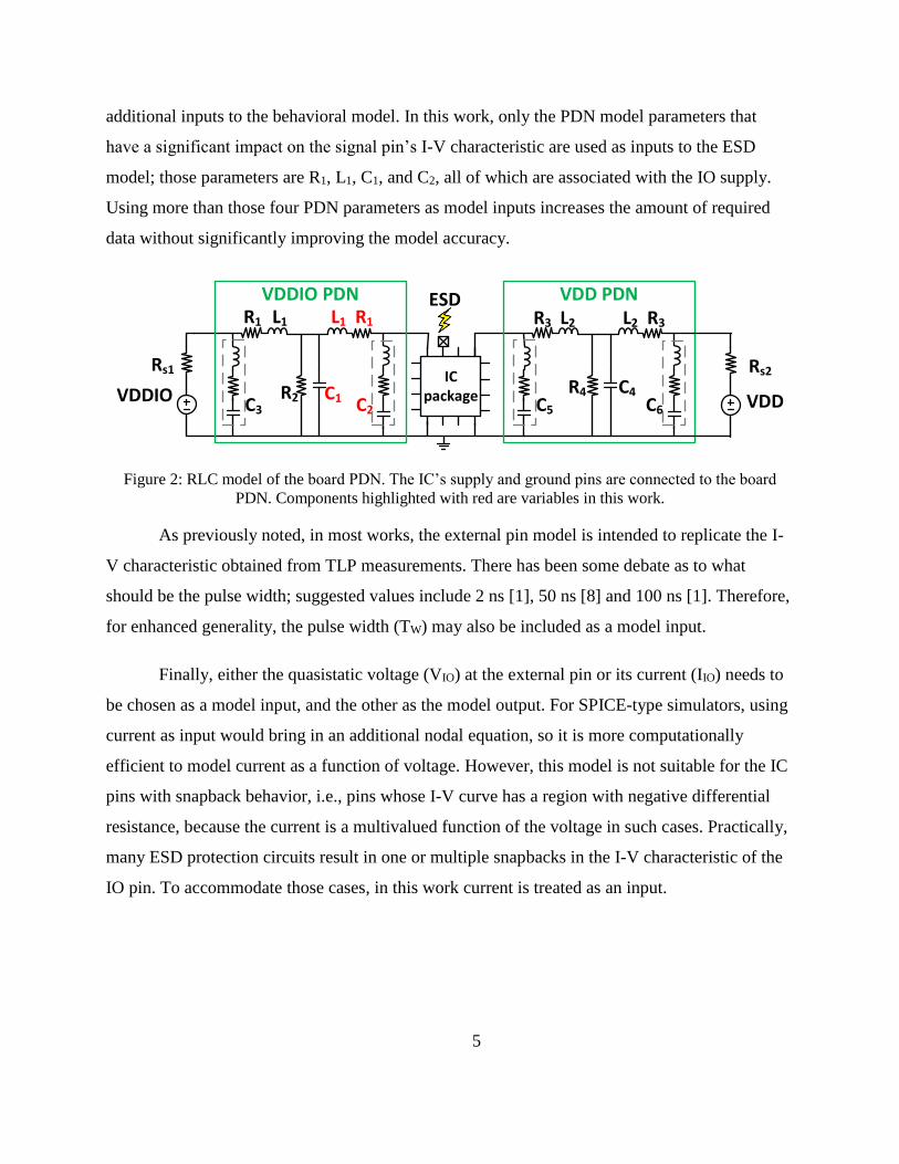
5
additional inputs to the behavioral model. In this work, only the PDN model parameters that
have a significant impact on the signal pin’s I-V characteristic are used as inputs to the ESD
model; those parameters are R1, L1, C1, and C2, all of which are associated with the IO supply.
Using more than those four PDN parameters as model inputs increases the amount of required
data without significantly improving the model accuracy.
Figure 2: RLC model of the board PDN. The IC’s supply and ground pins are connected to the board
PDN. Components highlighted with red are variables in this work.
As previously noted, in most works, the external pin model is intended to replicate the I-
V characteristic obtained from TLP measurements. There has been some debate as to what
should be the pulse width; suggested values include 2 ns [1], 50 ns [8] and 100 ns [1]. Therefore,
for enhanced generality, the pulse width (TW) may also be included as a model input.
Finally, either the quasistatic voltage (VIO) at the external pin or its current (IIO) needs to
be chosen as a model input, and the other as the model output. For SPICE-type simulators, using
current as input would bring in an additional nodal equation, so it is more computationally
efficient to model current as a function of voltage. However, this model is not suitable for the IC
pins with snapback behavior, i.e., pins whose I-V curve has a region with negative differential
resistance, because the current is a multivalued function of the voltage in such cases. Practically,
many ESD protection circuits result in one or multiple snapbacks in the I-V characteristic of the
IO pin. To accommodate those cases, in this work current is treated as an input.
R1 L1 L1
C1R2C3 C2
R1
IC package
R3 L2 L2
C4R4C5 C6
R3
ESDVDDIO PDN VDD PDN
Rs1
VDDIO
Rs2
VDD

6
2.3 Kernel Regression
Our goal is to generate a model with six inputs (IIO, TW, R1, L1, C1 and C2) and one output
(VIO). Statistical learning methods are preferred because it is a high-dimensional fitting problem.
Input-output training data can be obtained from TLP measurement or from circuit simulation.
Kernel regression is used to construct a non-parametric I-V model from the data. Kernel
regression is an effective method to tackle multivariable fitting problems, i.e., to estimate the
nonlinear relation between input-output pairs. The observed data can be taken as kernels. To
predict the output given a new input, all kernels are added up with different weights determined
by the distance between the kernel and the new input. The Nadaraya-Watson kernel estimator [9]
is expressed as follows.
�̂�𝒉(𝒙) =∑ 𝐾𝒉(𝒙 − 𝒙𝑖)𝑦𝑖𝑛𝑖=1
∑ 𝐾𝒉(𝒙 − 𝒙𝑖)𝑛𝑖=1
(1)
𝐾𝒉(𝒙) =∏𝑒− 12(𝑥𝑗ℎ𝑗)2𝑘
𝑗=1
(2)
Above, 𝒙𝑖, 𝑦𝑖 are input-output training samples and 𝑛 is the total number of training
samples. The terms 𝒙𝑖 and 𝑦𝑖 may be scalars or vectors; in this work, 𝒙𝑖 is a six-dimensional
vector and 𝑦𝑖 is a scalar, representing the output voltage. The kernel function 𝐾𝒉(𝒙) is selected
by the user; it must be symmetric and centered at 0. In this work, the Gaussian kernel is used.
Note that the constant coefficient of the Gaussian function is omitted, as it will be eliminated
after substituting the kernel function into the numerator and the denominator of eq. (1). Vector 𝒉
is the bandwidth of the kernel function, which is tuned by cross-validation to minimize the mean
square error [10]. 𝑘 is the dimensionality of 𝒙 and 𝒉, which is 6 in this work.
Equation (1) is used to estimate the conditional expected value of the output �̂� given the
input vector 𝒙. In essence, it constructs �̂� as a weighted average of all the training sample
outputs; the weight assigned to each 𝑦𝑖 is calculated with the kernel function and the distance
between 𝒙 and 𝒙𝑖.
7
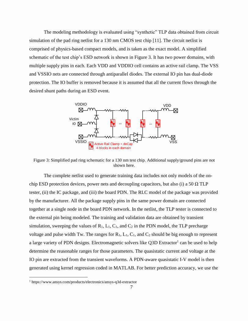
The modeling methodology is evaluated using “synthetic” TLP data obtained from circuit
simulation of the pad ring netlist for a 130 nm CMOS test chip [11]. The circuit netlist is
comprised of physics-based compact models, and is taken as the exact model. A simplified
schematic of the test chip’s ESD network is shown in Figure 3. It has two power domains, with
multiple supply pins in each. Each VDD and VDDIO cell contains an active rail clamp. The VSS
and VSSIO nets are connected through antiparallel diodes. The external IO pin has dual-diode
protection. The IO buffer is removed because it is assumed that all the current flows through the
desired shunt paths during an ESD event.
VDD
VSS
VDDIO
VSSIO
...
...
...
...
...
...
Active Rail Clamp + deCap
4 blocks in each domain
Victim IO
Figure 3: Simplified pad ring schematic for a 130 nm test chip. Additional supply/ground pins are not
shown here.
The complete netlist used to generate training data includes not only models of the on-
chip ESD protection devices, power nets and decoupling capacitors, but also (i) a 50 Ω TLP
tester, (ii) the IC package, and (iii) the board PDN. The RLC model of the package was provided
by the manufacturer. All the package supply pins in the same power domain are connected
together at a single node in the board PDN network. In the netlist, the TLP tester is connected to
the external pin being modeled. The training and validation data are obtained by transient
simulation, sweeping the values of R1, L1, C1, and C2 in the PDN model, the TLP precharge
voltage and pulse width Tw. The ranges for R1, L1, C1, and C2 should be big enough to represent
a large variety of PDN designs. Electromagnetic solvers like Q3D Extractor1 can be used to help
determine the reasonable ranges for those parameters. The quasistatic current and voltage at the
IO pin are extracted from the transient waveforms. A PDN-aware quasistatic I-V model is then
generated using kernel regression coded in MATLAB. For better prediction accuracy, we use the
1 https://www.ansys.com/products/electronics/ansys-q3d-extractor

8
logarithm of the current value for computation instead of the raw current because the current is
an exponential function of the voltage at low current levels. The kernel model is validated by
comparing its output (�̂�) in response to a previously unencountered input (𝒙) to the “true” output
(𝑦). The true output is obtained from circuit simulation of the complete system netlist using
physics-based compact models.
Figure 4 shows such a comparison for two systems with different PDNs, neither of which
were included in the training samples. In this example, the I-V characteristic of the pin under test
is strongly influenced by the board PDN design. The kernel model successfully captures the
effect of the board PDN; the kernel model output, i.e., the pin voltage, differs by less than 1%
from that obtained using the exact model. The relative error is calculated using Eq. (3) and
plotted in Figure 5.
δ =| �̂� − 𝑦|
𝑦× 100% (3)
Figure 4: I-V characteristic of the IC pin simulated using the kernel model and the exact model. The test
chip is mounted on two boards with different PDN designs: (1) R1 = 50 mΩ, L1 = 5 nH, C1 = 6 pF, C2 =
0.1 μF; (2) R1 = 50 mΩ, L1 = 12 nH, C1 = 6 pF, C2 = 0.3 μF.

9
Figure 5: Relative error for predicted voltages.
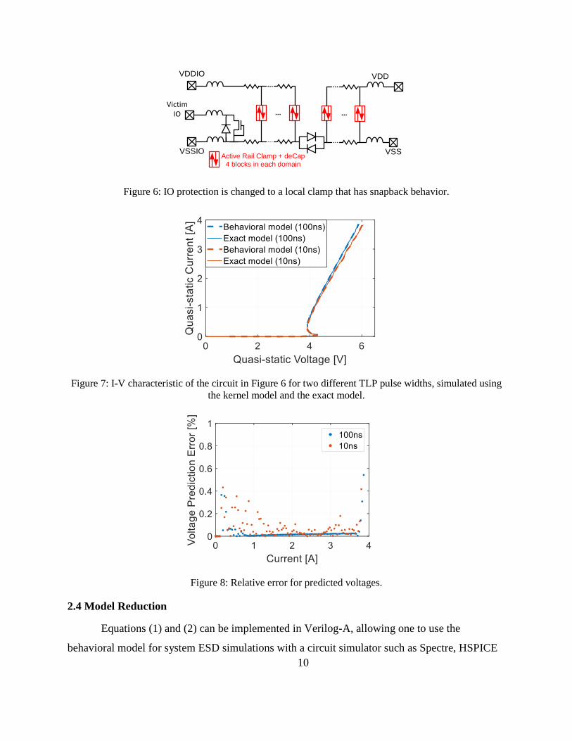
Although the IOs of the test chip were protected by dual-diodes, a second test case is
designed to validate the kernel model for IO pins with snapback. The netlist is similar to the first
test case, while the top diode is removed and a grounded-gate NMOS (ggNMOS) local clamp is
added in parallel with the bottom diode, as shown in Figure 6. The ggNMOS will not be
triggered until the parasitic NPN reaches the avalanche breakdown point. The ggNMOS shows
snapback behavior at this point.
We repeated the same procedure and obtained a PDN-aware quasistatic I-V model for the
second IC pin. In this case, for both polarities, the primary return path for the ESD current is
from VSSIO to the board. Therefore, the board PDN has less impact than in the first test case.
Instead of looking at the effect of board PDN, we show the difference made by different pulse
widths. In Figure 7, the I-V characteristic predicted by the kernel model is compared with that
provided by the exact model for two different TLP pulse widths. The voltage prediction error is
less than 1%, establishing that snapback-type protection can be well modeled, as is shown in
Figure 8.
10
VDD
VSS
VDDIO
VSSIO
...
...
...
...
...
...
Active Rail Clamp + deCap
4 blocks in each domain
Victim IO
Figure 6: IO protection is changed to a local clamp that has snapback behavior.
Figure 7: I-V characteristic of the circuit in Figure 6 for two different TLP pulse widths, simulated using
the kernel model and the exact model.
Figure 8: Relative error for predicted voltages.
2.4 Model Reduction
Equations (1) and (2) can be implemented in Verilog-A, allowing one to use the
behavioral model for system ESD simulations with a circuit simulator such as Spectre, HSPICE

11
or ADS. However, as is evident from eq. (1), the complexity of the model will increase linearly
with 𝑛, the number of training samples. For improved computational efficiency, a less complex
model can be fit to the kernel model for a given system implementation, e.g., a specific board
PDN design. The low complexity model may be as simple as a piecewise linear model.
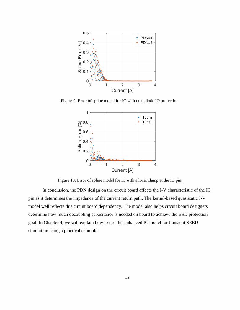
Here, we demonstrate using spline functions to construct a reduced complexity, system-
specific model. Spline interpolation is capable of approximating the kernel model for a wide
variety of I-V curves. In each spline interval, cubic Hermite interpolation (CHI) is used to obtain
a third-order polynomial fitting function. CHI fits the observed value of 𝑦𝑖 as well as its first
derivative over 𝒙𝑖, so it can preserve the shape of the curve and alleviate the overfitting problem
commonly encountered with other interpolation methods. To ensure a physically reasonable
result, the model is extrapolated linearly at current levels that exceed the maximum value among
the training data. The spline model can be written in the following form:
�̂�(𝐼) =
{
𝐴𝐼 + 𝐵 𝐼 < 𝐼−𝑁
𝑎𝑗(𝐼 − 𝐼𝑗)3+ 𝑏𝑗(𝐼 − 𝐼𝑗)
2+𝑐𝑗(𝐼 − 𝐼𝑗) + 𝑑𝑗 𝐼𝑗 ≤ 𝐼 < 𝐼𝑗+1 (𝑗 = −𝑁,… , 𝑁)
𝐶𝐼 + 𝐷 𝐼 > 𝐼𝑁
(4)
Above, (2𝑁) is the number of spline intervals and A, B, C, D, aj, bj, cj and dj are fitting
parameters. The model complexity is independent of the number of data samples; the number of
spline intervals (2𝑁) depends on the fitting accuracy the user wants to achieve. 𝑁 is 100 in this
work to provide an accurate fit for TLP currents in the range of 1 mA to 4 A, and for both
polarities. The model of eq. (4) can be implemented in Verilog-A and applied to SEED-type
simulation. We compared the voltage predicted by the kernel model and the reduced complexity
model generated using MATLAB’s built-in spline function. Figure 9 and Figure 10 show the
spline interpolation error for the test cases in Figure 3 and Figure 6 respectively. The very small
error values indicate that spline approximation does not sacrifice accuracy.
12
Figure 9: Error of spline model for IC with dual diode IO protection.
Figure 10: Error of spline model for IC with a local clamp at the IO pin.
In conclusion, the PDN design on the circuit board affects the I-V characteristic of the IC
pin as it determines the impedance of the current return path. The kernel-based quasistatic I-V
model well reflects this circuit board dependency. The model also helps circuit board designers
determine how much decoupling capacitance is needed on board to achieve the ESD protection
goal. In Chapter 4, we will explain how to use this enhanced IC model for transient SEED
simulation using a practical example.
13
CHAPTER 3: IMPROVED IEC 61000-4-2 ESD SOURCE MODEL
3.1 IEC 61000-4-2 Test Setup
The International Electrotechnical Commission (IEC) stipulates a reproducible test
standard to evaluate the performance of electronic equipment when subjected to ESD [12]. The
standard gives specifications for the discharge current waveform, the range of test levels, the test
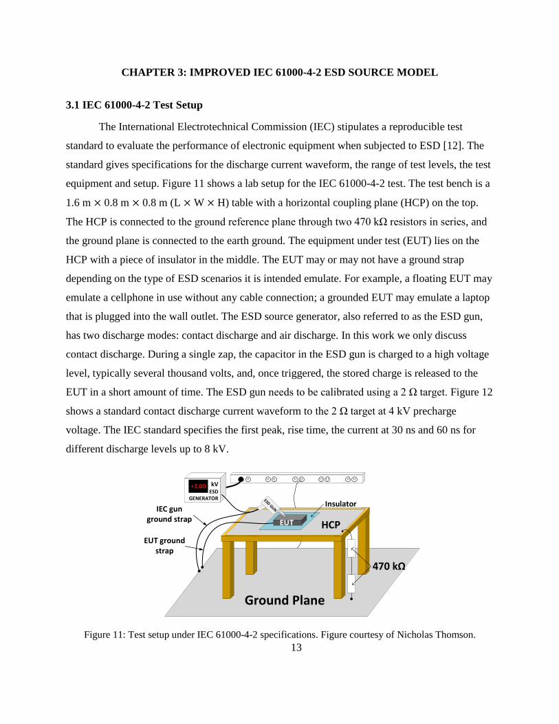
equipment and setup. Figure 11 shows a lab setup for the IEC 61000-4-2 test. The test bench is a
1.6 m × 0.8 m × 0.8 m (L × W × H) table with a horizontal coupling plane (HCP) on the top.
The HCP is connected to the ground reference plane through two 470 kΩ resistors in series, and
the ground plane is connected to the earth ground. The equipment under test (EUT) lies on the
HCP with a piece of insulator in the middle. The EUT may or may not have a ground strap
depending on the type of ESD scenarios it is intended emulate. For example, a floating EUT may
emulate a cellphone in use without any cable connection; a grounded EUT may emulate a laptop
that is plugged into the wall outlet. The ESD source generator, also referred to as the ESD gun,
has two discharge modes: contact discharge and air discharge. In this work we only discuss
contact discharge. During a single zap, the capacitor in the ESD gun is charged to a high voltage
level, typically several thousand volts, and, once triggered, the stored charge is released to the
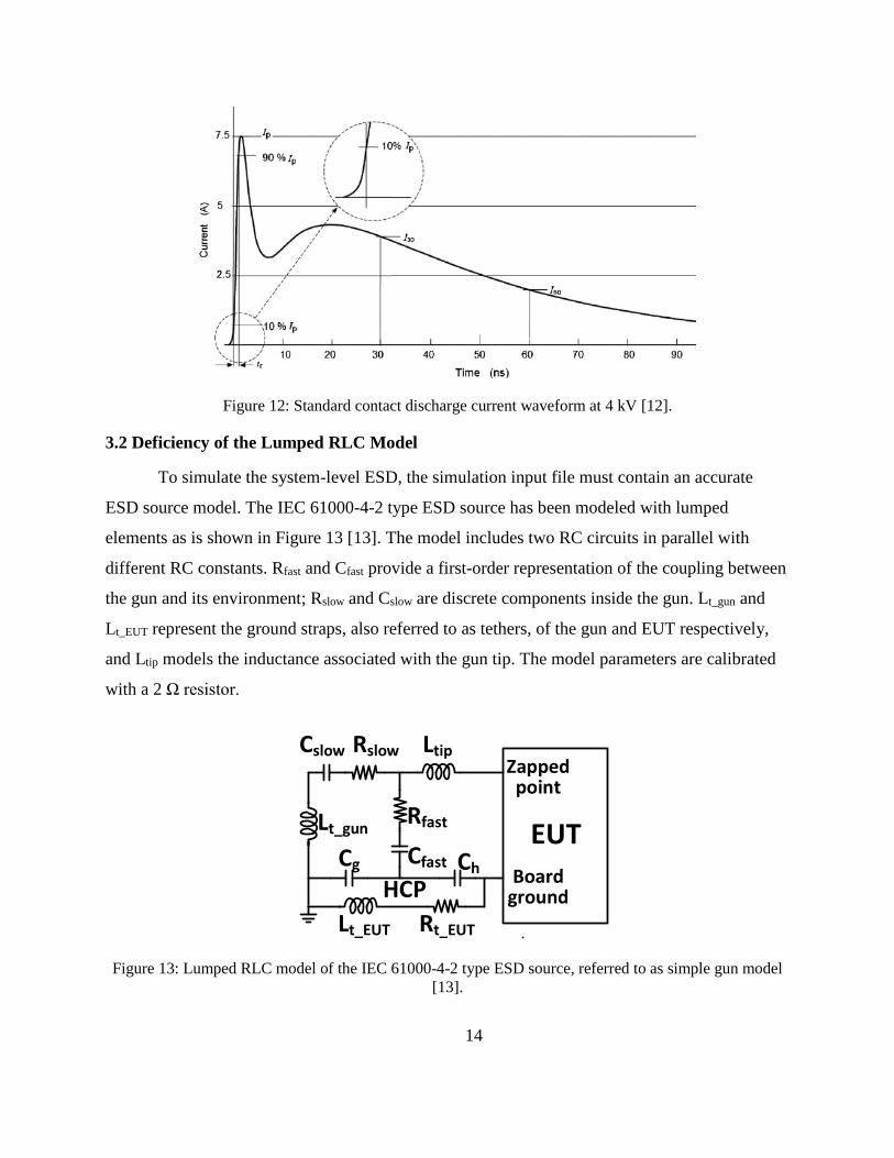
EUT in a short amount of time. The ESD gun needs to be calibrated using a 2 Ω target. Figure 12
shows a standard contact discharge current waveform to the 2 Ω target at 4 kV precharge
voltage. The IEC standard specifies the first peak, rise time, the current at 30 ns and 60 ns for
different discharge levels up to 8 kV.
Figure 11: Test setup under IEC 61000-4-2 specifications. Figure courtesy of Nicholas Thomson.
kVESD
GENERATOR
+2.00
EUT HCP
Ground Plane
Insulator
470 kΩ
IEC gun ground strap
EUT ground strap
14
Figure 12: Standard contact discharge current waveform at 4 kV [12].
3.2 Deficiency of the Lumped RLC Model
To simulate the system-level ESD, the simulation input file must contain an accurate
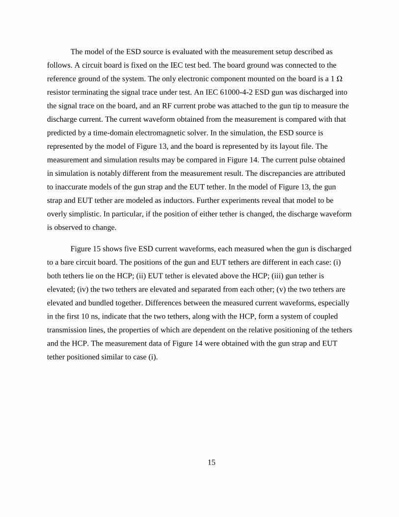
ESD source model. The IEC 61000-4-2 type ESD source has been modeled with lumped
elements as is shown in Figure 13 [13]. The model includes two RC circuits in parallel with
different RC constants. Rfast and Cfast provide a first-order representation of the coupling between
the gun and its environment; Rslow and Cslow are discrete components inside the gun. Lt_gun and
Lt_EUT represent the ground straps, also referred to as tethers, of the gun and EUT respectively,
and Ltip models the inductance associated with the gun tip. The model parameters are calibrated
with a 2 Ω resistor.
EUT
Zapped point
Board ground
Ltip
Cfast
Rfast
Cslow Rslow
Lt_gun
Ch
Rt_EUTLt_EUT
Cg
HCP
Figure 13: Lumped RLC model of the IEC 61000-4-2 type ESD source, referred to as simple gun model
[13].
15
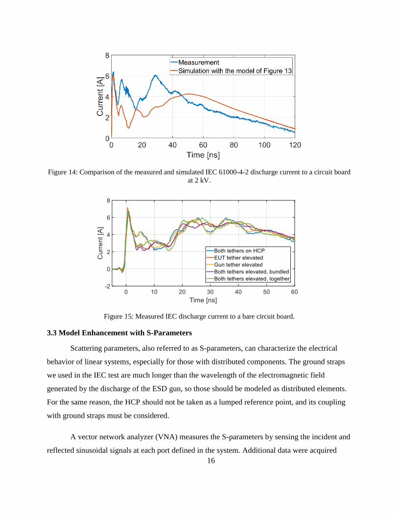
The model of the ESD source is evaluated with the measurement setup described as
follows. A circuit board is fixed on the IEC test bed. The board ground was connected to the
reference ground of the system. The only electronic component mounted on the board is a 1 Ω
resistor terminating the signal trace under test. An IEC 61000-4-2 ESD gun was discharged into
the signal trace on the board, and an RF current probe was attached to the gun tip to measure the
discharge current. The current waveform obtained from the measurement is compared with that
predicted by a time-domain electromagnetic solver. In the simulation, the ESD source is
represented by the model of Figure 13, and the board is represented by its layout file. The
measurement and simulation results may be compared in Figure 14. The current pulse obtained
in simulation is notably different from the measurement result. The discrepancies are attributed
to inaccurate models of the gun strap and the EUT tether. In the model of Figure 13, the gun
strap and EUT tether are modeled as inductors. Further experiments reveal that model to be
overly simplistic. In particular, if the position of either tether is changed, the discharge waveform
is observed to change.
Figure 15 shows five ESD current waveforms, each measured when the gun is discharged
to a bare circuit board. The positions of the gun and EUT tethers are different in each case: (i)
both tethers lie on the HCP; (ii) EUT tether is elevated above the HCP; (iii) gun tether is
elevated; (iv) the two tethers are elevated and separated from each other; (v) the two tethers are
elevated and bundled together. Differences between the measured current waveforms, especially
in the first 10 ns, indicate that the two tethers, along with the HCP, form a system of coupled
transmission lines, the properties of which are dependent on the relative positioning of the tethers
and the HCP. The measurement data of Figure 14 were obtained with the gun strap and EUT
tether positioned similar to case (i).
16
Figure 14: Comparison of the measured and simulated IEC 61000-4-2 discharge current to a circuit board
at 2 kV.
Figure 15: Measured IEC discharge current to a bare circuit board.
3.3 Model Enhancement with S-Parameters
Scattering parameters, also referred to as S-parameters, can characterize the electrical
behavior of linear systems, especially for those with distributed components. The ground straps
we used in the IEC test are much longer than the wavelength of the electromagnetic field
generated by the discharge of the ESD gun, so those should be modeled as distributed elements.
For the same reason, the HCP should not be taken as a lumped reference point, and its coupling
with ground straps must be considered.
A vector network analyzer (VNA) measures the S-parameters by sensing the incident and
reflected sinusoidal signals at each port defined in the system. Additional data were acquired

17
from two-port S-parameter measurements (300 kHz – 2 GHz) for use in improving the gun
model. The setup is shown in Figure 16; two 10-foot ground strap cables are used to represent
the ESD gun strap and EUT tether. The cables are positioned similarly to case (i) described
above. One end of each cable is connected to the center conductor of an SMA connecter, and the
far end is terminated at the ground plane. The center of the HCP is set as the common reference
for the two ports; thus, the outer shields of both SMAs are fixed on the center of the HCP with
conductive tape (not shown in the figure). The S-parameters are measured at the two SMA ports,
with everything to the right of those connectors de-embedded. The VNA has its own reference
ground, so the ground plane needs to be disconnected from the earth ground to prevent an
undesired return path.
An equivalent SPICE model is generated from the measured S-parameters using ADS.
The SPICE model of the tethers is inserted into the ESD gun model, resulting in the enhanced
model shown in Figure 17(b). The simulated current obtained using the enhanced model is
plotted in Figure 18, together with the data in Figure 14 for comparison. Although both the
simple gun model and the enhanced gun model replicate the first current peak, the enhanced gun
model provides a significantly closer representation of the measured waveform after 5 ns.
Discrepancy between simulation and measurement still exists, and the possible explanations are:
(i) The “mock” ground straps have different characteristic impedance and/or propagation delay
than the actual ground straps of the gun and EUT. (ii) When we measured the S-parameters, the
positions of the ground straps did not exactly match the IEC test setup we used. (iii) The S-
parameters lack low-frequency information of the ground straps.
The IEC standard does not dictate the exact position of the gun strap or an EUT tether.
The S-parameter-based modeling of those return paths can improve the waveform fidelity
obtained from simulation, but precise agreement with measurement should not be expected given
the uncertainty regarding the real-world measurement setup.

18
HCP
Ground Plane
470 kΩ
VNAIEC gun
ground strap
EUT ground strap
Figure 16: S-parameter measurement setup.
EUT
Zapped point
Board ground
Ltip
Cfast
Rfast
Cslow Rslow
Lt_gun
Ch
Rt_EUTLt_EUT
EUT
Zapped point
Cfast
Rfast
Ch
S-parameter model of gun
and EUT tethersP2P1
HCPCg
Cslow
Rslow
Board groundHCP
(a) (b)
Figure 17: (a) Simple gun model. (b) Enhanced gun model. The elements highlighted in red are models
for the gun and EUT ground straps (tethers).
Figure 18: Measured and simulated IEC discharge current to a circuit board.

19
CHAPTER 4: PRACTICAL SYSTEM MODELING APPROACH
In this chapter, we will elaborate the modeling approach for system-level ESD using a
custom ESD test board as an example. We will apply the IC component and ESD source models
discussed in Chapters 2 and 3 respectively to this test case. We will also discuss a continuous
snapback model which overcomes the convergence problem in simulation. This methodology
will be validated by comparing the simulation results with measurement data obtained from IEC-
type ESD test.
4.1 Overview of the Test System
A USB 3.0 test circuit board is the equipment under test (EUT) in this work. It is
provided by EOS/ESD Association Working Group 262 for multiple laboratories to develop
advanced ESD models for system-level ESD simulation. The top view of the test board is shown
in Figure 19. The board has a USB IC mounted on the center. Two pins on the IC can be zapped
through the USB port on the right side of the board. They are one pin of the transceiver
differential pair (TX) and one pin of the receiver differential pair (RX). Each pin under test has a
1.1 kV pick-off resistor on the board. The resistor is put as close to the chip pin as possible to
measure the voltage. The board provides a coupling structure to measure the inductive current,
but in this work, the current is measured using an external current probe. At the bottom of the
board is a calibration structure, with which we have done open, short and 50 Ω calibration before
the test. The voltage regulator on the top left of the board can provide a 3.3 V supply for the IC.
We only present the power-off case in this thesis, and the modeling approach for the IC in
power-on state is similar. One should notice that the quasistatic I-V of the IC signal pins would
shift by around 3.3 V (VDD) in the power-on state, so it needs to be modeled using the TLP data
measured with the power supply on. An injection board, shown in Figure 20, is used to connect
the main test board to the ESD generator, which is a TLP tester. During an ESD test, the
injection board sends the discharge current to the main board. The current enters the USB IC and
finally returns to the board ground through the board PDN.
2 https://www.esda.org/committees/standards-working-groups/wg26/

20
Figure 19: The top view of the USB 3.0 test board, with a USB IC (DUT) mounted on the center. ESD
current is injected from the USB port on the right.
Figure 20: ESD injection board connected to the test board through the USB port on the right. ESD
current can be injected from the two SMA ports.

21
4.2 IC Signal Pin Model
The IC pin needs to be characterized using TLP measurement. The TLP test setup is as
follows: The TLP output is connected to one of the SMA connectors on the injection board, with
a CT1 current probe in between; the voltage pick-off is connected to a 12 GHz oscilloscope.
To generate a PDN-aware I-V model, we consider the variability of the circuit board
PDN. Since only one test board is used in this study, the only factor that can affect its PDN
impedance is the amount of decoupling capacitance that is included on the board. The board is
designed to have at most four surface mount capacitors at the chip side. The sum of those near-
chip capacitances is the only important factor; the PDN impedance does not depend on whether
the capacitance is uniformly or nonuniformly distributed among the four sites, because the chip
size is much smaller than the board. Therefore, in the experiment, we vary the capacitance at one
spot instead of doing all the combinations of different capacitances at the four locations. The
decoupling capacitors near the voltage regulator are not changed in these experiments, although
they may also affect the behavior of the IC pin. We consider that, practically, one should put
enough capacitance at the output of the voltage regulator, as is specified in the data manual. Any
failure due to improper usage of the voltage regulator is not considered here.
It turns out from measurement that the TX and RX have similar ESD responses, so we
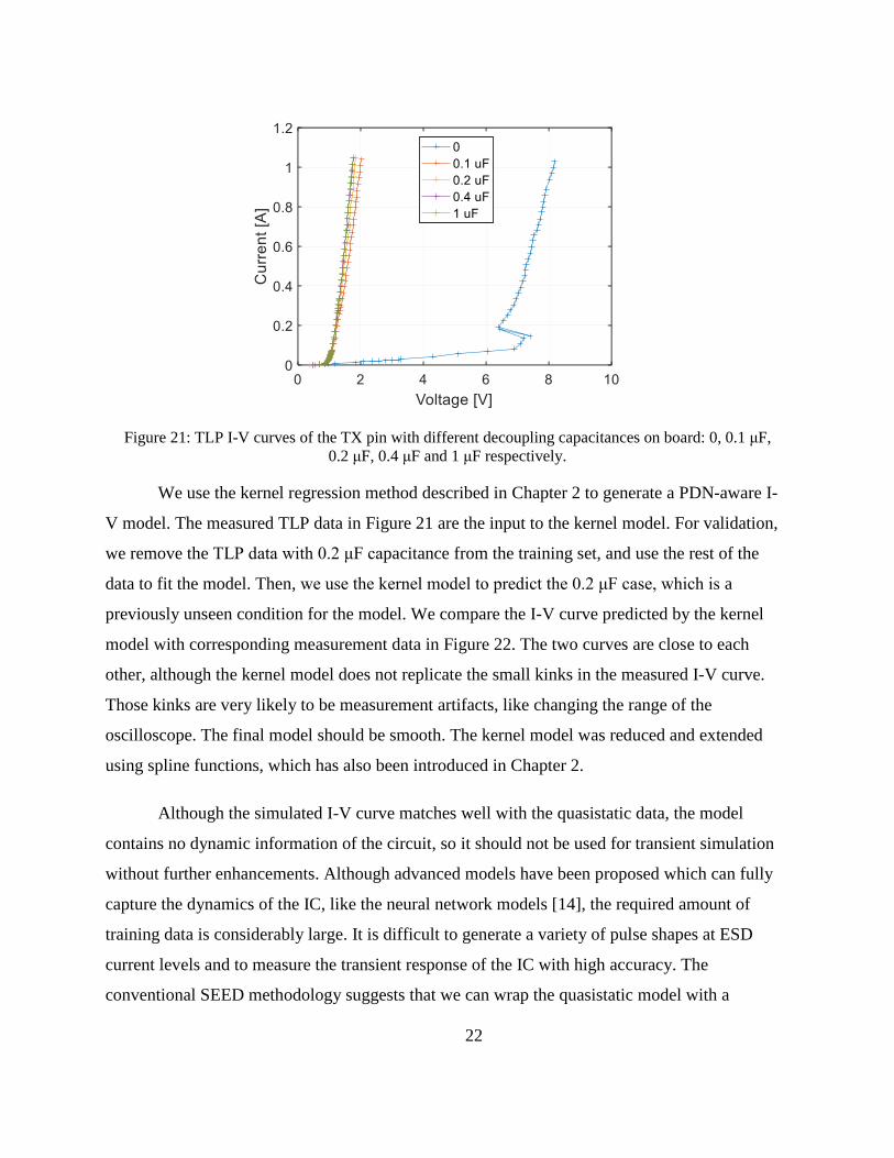
only present results obtained by zapping the TX. Figure 21 shows the TLP I-V of the TX pin
under five different board conditions. When there is zero decoupling capacitance near the chip,
the IC pin has snapback behavior, and its I-V curve seriously deviates from other cases. When
one puts no capacitors near the chip, the impedance seen by VDD pins of the chip becomes
significantly larger. The ESD current in the chip tends to choose the return path with lower
impedance. Therefore, instead of returning to the board through VDD pins, it flows to the VSS
nets in the chip through power rail clamps on chip, and finally returns to the board ground
through VSS pins. The snapback is a property of the full chip protection network, and the large
deviation is a result of the higher clamping voltage of the rail clamps and the voltage drop on the
supply nets. The I-V curves with capacitance greater than 0.4 μF are overlapped with each other,
indicating that, from this point, the IC pin would not clamp at a lower voltage by adding extra
capacitance.
22
Figure 21: TLP I-V curves of the TX pin with different decoupling capacitances on board: 0, 0.1 μF,
0.2 μF, 0.4 μF and 1 μF respectively.
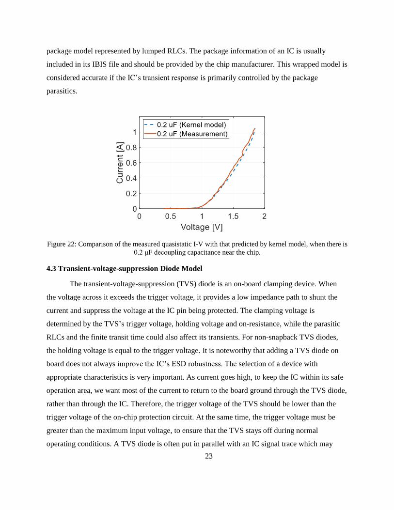
We use the kernel regression method described in Chapter 2 to generate a PDN-aware I-
V model. The measured TLP data in Figure 21 are the input to the kernel model. For validation,
we remove the TLP data with 0.2 μF capacitance from the training set, and use the rest of the
data to fit the model. Then, we use the kernel model to predict the 0.2 μF case, which is a
previously unseen condition for the model. We compare the I-V curve predicted by the kernel
model with corresponding measurement data in Figure 22. The two curves are close to each
other, although the kernel model does not replicate the small kinks in the measured I-V curve.
Those kinks are very likely to be measurement artifacts, like changing the range of the
oscilloscope. The final model should be smooth. The kernel model was reduced and extended
using spline functions, which has also been introduced in Chapter 2.
Although the simulated I-V curve matches well with the quasistatic data, the model
contains no dynamic information of the circuit, so it should not be used for transient simulation
without further enhancements. Although advanced models have been proposed which can fully
capture the dynamics of the IC, like the neural network models [14], the required amount of
training data is considerably large. It is difficult to generate a variety of pulse shapes at ESD
current levels and to measure the transient response of the IC with high accuracy. The
conventional SEED methodology suggests that we can wrap the quasistatic model with a
23
package model represented by lumped RLCs. The package information of an IC is usually
included in its IBIS file and should be provided by the chip manufacturer. This wrapped model is
considered accurate if the IC’s transient response is primarily controlled by the package
parasitics.
Figure 22: Comparison of the measured quasistatic I-V with that predicted by kernel model, when there is
0.2 μF decoupling capacitance near the chip.
4.3 Transient-voltage-suppression Diode Model
The transient-voltage-suppression (TVS) diode is an on-board clamping device. When
the voltage across it exceeds the trigger voltage, it provides a low impedance path to shunt the
current and suppress the voltage at the IC pin being protected. The clamping voltage is
determined by the TVS’s trigger voltage, holding voltage and on-resistance, while the parasitic
RLCs and the finite transit time could also affect its transients. For non-snapback TVS diodes,
the holding voltage is equal to the trigger voltage. It is noteworthy that adding a TVS diode on
board does not always improve the IC’s ESD robustness. The selection of a device with
appropriate characteristics is very important. As current goes high, to keep the IC within its safe
operation area, we want most of the current to return to the board ground through the TVS diode,
rather than through the IC. Therefore, the trigger voltage of the TVS should be lower than the
trigger voltage of the on-chip protection circuit. At the same time, the trigger voltage must be
greater than the maximum input voltage, to ensure that the TVS stays off during normal
operating conditions. A TVS diode is often put in parallel with an IC signal trace which may
24
suffer from ESD stress. Practically, it should be put as close to the board edge as possible, to
minimize the current loop and the coupling to other traces on board.
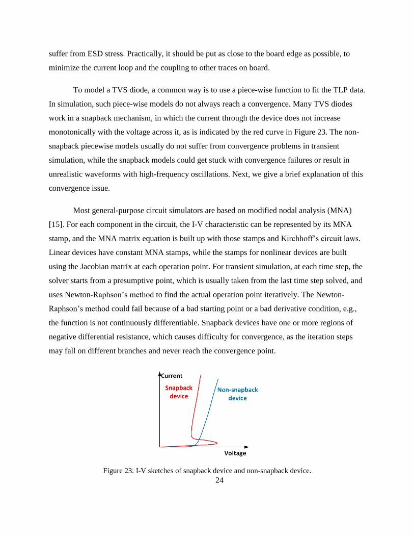
To model a TVS diode, a common way is to use a piece-wise function to fit the TLP data.
In simulation, such piece-wise models do not always reach a convergence. Many TVS diodes
work in a snapback mechanism, in which the current through the device does not increase
monotonically with the voltage across it, as is indicated by the red curve in Figure 23. The non-
snapback piecewise models usually do not suffer from convergence problems in transient
simulation, while the snapback models could get stuck with convergence failures or result in
unrealistic waveforms with high-frequency oscillations. Next, we give a brief explanation of this
convergence issue.
Most general-purpose circuit simulators are based on modified nodal analysis (MNA)
[15]. For each component in the circuit, the I-V characteristic can be represented by its MNA
stamp, and the MNA matrix equation is built up with those stamps and Kirchhoff’s circuit laws.
Linear devices have constant MNA stamps, while the stamps for nonlinear devices are built
using the Jacobian matrix at each operation point. For transient simulation, at each time step, the
solver starts from a presumptive point, which is usually taken from the last time step solved, and
uses Newton-Raphson’s method to find the actual operation point iteratively. The Newton-
Raphson’s method could fail because of a bad starting point or a bad derivative condition, e.g.,
the function is not continuously differentiable. Snapback devices have one or more regions of
negative differential resistance, which causes difficulty for convergence, as the iteration steps
may fall on different branches and never reach the convergence point.
Figure 23: I-V sketches of snapback device and non-snapback device.
25
The TVS diode (Nexperia PESD5V0C1USF) we placed on the test board has a deep
snapback. To overcome the convergence difficulty, we use a modeling framework for snapback
devices, which is designed to be convergence-friendly [16]. In the model, an internal state
variable which controls the turn-on/off behavior is solved from a continuous differential equation
containing a hyperbolic tangent. The fold in the DC solution of this equation creates the
snapback in the I-V curve. The input to the hyperbolic tangent has been modified in this work to
better fit the deep snapback. The expression of the shifted voltage (𝑉∗) is changed, and an
additional parameter 𝛾 is added to increase the variability of the snapback shape. The modified
model is expressed as follows.
τ (𝑑
𝑑𝑡𝑠∗) = tanh(𝐾 ∙ (𝑉∗ + 𝛾 ∙ 𝑠∗)) − 𝑠∗ (5)
𝑠∗ = 2𝑠 − 1 (6)
𝑉∗ =2
𝑉𝑡 − 𝑉ℎ(𝑉 − 𝑉ℎ) (7)
Above, 𝑠 is the internal state variable which controls the state transition. Finally, the
current (𝐼) is expressed as a function of voltage (𝑉) and 𝑠, using the equations presented in [16]:
𝐼 =𝑑
𝑑𝑡(𝐶 ∙ 𝑉) + 𝐼𝑜𝑓𝑓 +
𝑠𝛼 + 𝛽 ∙ 𝑠
1 + 𝛽∙ 𝐼𝑜𝑛 (8)
𝐼𝑜𝑓𝑓 = 𝐼𝑠 ∙ 𝑒−𝑉𝑉𝑇 ∙ √1 +
max(𝑉, 0)
𝑉𝐷 (9)
𝐼𝑜𝑛 = 𝐼ℎ + 𝐺𝑜𝑛 ∙ (𝑉 − 𝑉ℎ) (10)
𝑉𝑇 is the thermal voltage. 𝑉𝑡, 𝑉ℎ, 𝐼ℎ and 𝐺𝑜𝑛 are extracted from the TLP I-V curve. 𝐾, 𝛼, 𝛽, 𝛾, 𝐼𝑠
and 𝑉𝐷 are fitting parameters, and are optimized to fit measurement data. 𝐶 and τ affect the
device dynamics and should be adjusted according to the measured transient behavior. The
model has been implemented in Verilog-A using a similar approach as is shown in [16], in which
a hidden node is added whose voltage represents the value of 𝑠.

26
We fit the model parameters with the measured TLP data of the TVS diode. Figure 24
shows the simulated TLP I-V of the model along with the measurement data. The measurement
does not yield any data points within the negative-resistance region because we use a 50 Ω TLP
system, and the operating points lie at the intersection of the 50 Ω load line and the DUT’s I-V
curves. The uncertainty of the holding voltage and current could introduce error into the TVS
model.
Ih
Vh Vt
Slope = Gon
Figure 24: Proposed TVS snapback model fitted to TLP data.
4.4 System Simulation Results
The system-level ESD test setup follows the IEC61000-4-2 standard introduced in
Chapter 3. The board is in power-off mode and connected to the injection board. The ESD gun
discharges to the injection board. A current probe is attached to the gun tip. A 2.5 GHz
oscilloscope is used to measure the voltage at the pick-off tee and the signal from the current
probe simultaneously. The board is tethered to the ground by the shield of the coaxial cable
connecting the voltage pick-off to the oscilloscope.
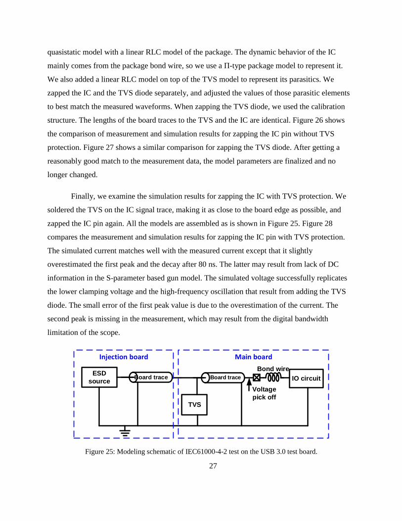
Figure 25 shows the modeling schematic of the system described above. The ESD source
is modeled using the enhanced model presented in Chapter 3. The board trances are modeled as
lossy transmission lines. The voltage pick-off resistor is also added. The quasistatic models for
the pin under stress and the TVS diode were elaborated in sections 4.2 and 4.3 respectively.
However, modeling the IC and the TVS with quasistatic models is not expected to yield accurate
results in IEC test simulation. To capture the dynamics, it is customary to augment the
27
quasistatic model with a linear RLC model of the package. The dynamic behavior of the IC
mainly comes from the package bond wire, so we use a Π-type package model to represent it.
We also added a linear RLC model on top of the TVS model to represent its parasitics. We
zapped the IC and the TVS diode separately, and adjusted the values of those parasitic elements
to best match the measured waveforms. When zapping the TVS diode, we used the calibration
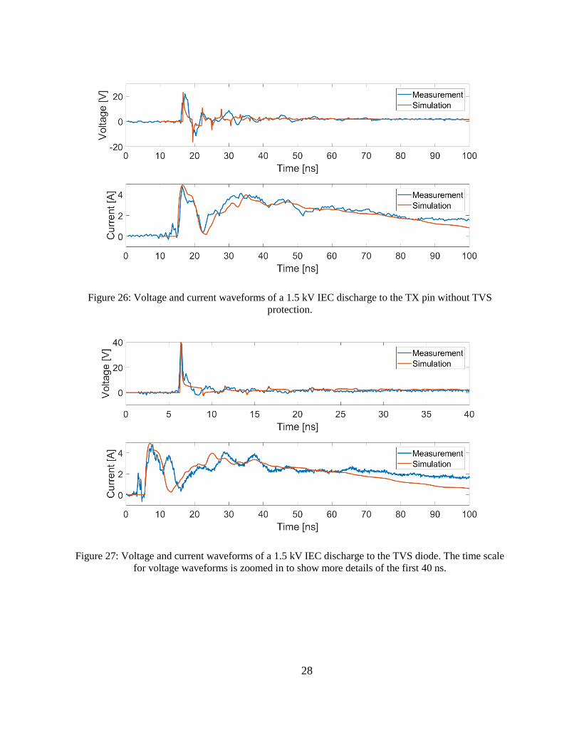
structure. The lengths of the board traces to the TVS and the IC are identical. Figure 26 shows
the comparison of measurement and simulation results for zapping the IC pin without TVS
protection. Figure 27 shows a similar comparison for zapping the TVS diode. After getting a
reasonably good match to the measurement data, the model parameters are finalized and no
longer changed.
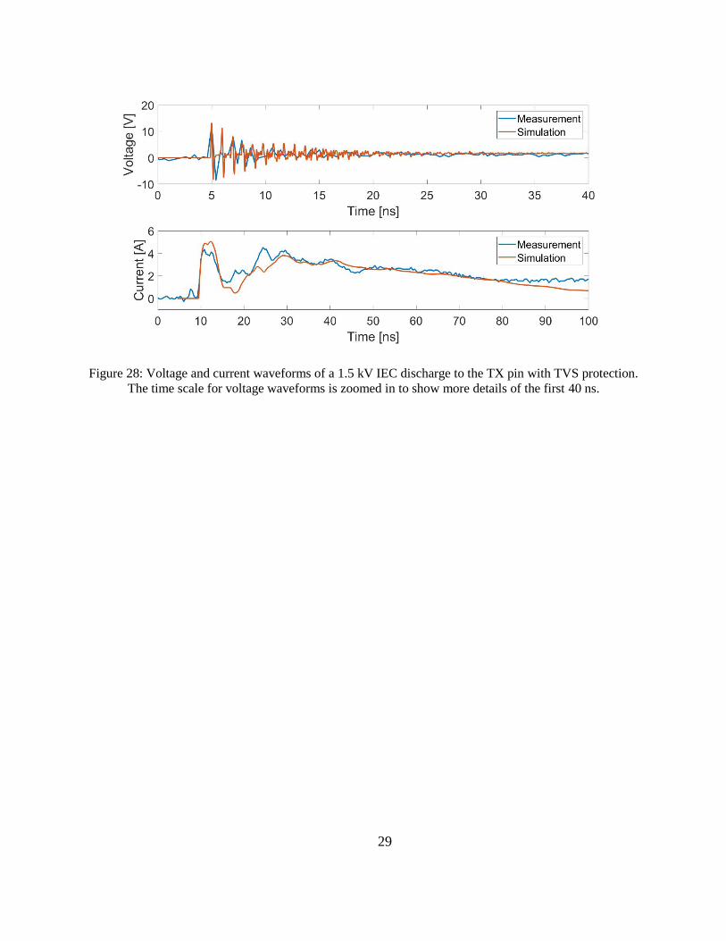
Finally, we examine the simulation results for zapping the IC with TVS protection. We
soldered the TVS on the IC signal trace, making it as close to the board edge as possible, and
zapped the IC pin again. All the models are assembled as is shown in Figure 25. Figure 28
compares the measurement and simulation results for zapping the IC pin with TVS protection.
The simulated current matches well with the measured current except that it slightly
overestimated the first peak and the decay after 80 ns. The latter may result from lack of DC
information in the S-parameter based gun model. The simulated voltage successfully replicates
the lower clamping voltage and the high-frequency oscillation that result from adding the TVS
diode. The small error of the first peak value is due to the overestimation of the current. The
second peak is missing in the measurement, which may result from the digital bandwidth
limitation of the scope.
ESD
source
TVS
IO circuitBoard trace Board trace
Bond wire
Voltage
pick off
Injection board Main board
Figure 25: Modeling schematic of IEC61000-4-2 test on the USB 3.0 test board.
28
Figure 26: Voltage and current waveforms of a 1.5 kV IEC discharge to the TX pin without TVS
protection.
Figure 27: Voltage and current waveforms of a 1.5 kV IEC discharge to the TVS diode. The time scale
for voltage waveforms is zoomed in to show more details of the first 40 ns.
29
Figure 28: Voltage and current waveforms of a 1.5 kV IEC discharge to the TX pin with TVS protection.
The time scale for voltage waveforms is zoomed in to show more details of the first 40 ns.

30
CHAPTER 5: ESD NOISE COUPLING ANALYSIS
In the previous three chapters, we have discussed advanced models and simulation
approaches that are useful for identifying potential ESD-induced hard failures. The simulation
results help the users to ensure that the IC stays in the SOA during an ESD event and prevent it
from being physically damaged. However, this method assumes zero coupling among package
pins and lumps all the pins in the same power domain together. Therefore, it cannot provide any
information of ESD-induced noise coupling. Even if the main ESD current pulse does not disturb
the proper functioning of the circuit, it may induce noise or glitches on neighboring signal lines
and thereby cause soft failures. It has been shown that bond wires and signal traces inside the IC
package are especially susceptible to the noise coupling [17]. The noise is coupled from the
zapped trace and the multiple return paths.
In this work, we focus on the package-level ESD-induced noise. To accurately simulate
ESD-induced noise coupling to signal lines, the multiple current return paths in the package must
be modeled, rather than lumping them together as in previous chapters. Furthermore, the
simulation should capture the return paths’ time dependency, e.g., a rail clamp may be on for
only part of the discharge event and this will cause the current division among the various return
paths to change as a function of time. Time-domain EM simulation tools are best suited for this
type of analysis. In this work, we use Speed2000.3 The analysis is undertaken for the case of IEC
61000-4-2 type ESD and, thus, the simulation input file must contain an ESD source model from
Chapter 3.
The package traces can be modeled and simulated in Speed2000. The die-level model
must allocate the correct fraction of the return current to each of those traces. Figure 29 shows
the proposed template for the die-level model; each of the red boxes in the figure represents a
protection circuit. The protection circuit may be represented by a model that describes its exact
schematic, i.e. a traditional circuit model, or by a behavioral or physical model, such as a PWL-
TR model [18], RNN model [19], or the kernel model presented in Chapter 2. The class of model
3 https://www.cadence.com/content/cadence-www/global/en_US/home/tools/ic-package-design-and-analysis/si-pi-
analysis-point-tools/sigrity-speed2000.html

31
selected must be compatible with the simulator to be used. Proof of concept for the proposed
approach is provided below.
IO
protection
Rail
Clamp
I/O pin VDD pin
Bus1Bus2Bus3
(b) Partial ESD Network Example
VSS pin
Behavioral
Model
(a) Pin ModelVDDIOVDDVSS
Figure 29: Proposed template for die-level models. (a) General model structure of a pin. (b) Example of
three instances of the pin model.
IO0(stressed)
VSSIO
VDDIO
VSS
VDD Die model
IO1
IO2
IO3
Figure 30: Flip chip package model (EM) connected to a synthetic die model (SPICE). The IO0 trace in
the package is 9.5 mm with 5.2 nH inductance, and the longest VDDIO/VSSIO trace is 0.77 mm with
0.4 nH inductance.
A test case is constructed for a 144-pin flip chip package model whose layout is shown in
Figure 30. A synthetic multi-port die model is constructed with 4 VDDIO, 4 VSSIO, 4 VDD, 4

32
VSS and 4 IO cells. There is a rail clamp in each power cell. The input circuitry of each IO cell
is represented by a 300 fF capacitor and is protected by dual diodes. SPICE models are used for
all semiconductor devices. IO0 is designated as the external pin (zap pin); IO1-IO3 are the victim
IOs that may suffer from coupled noise. The IO1 trace in the package is close to the IO0 trace.
IO2 and IO3 are close to VDDIO and VSSIO traces, respectively. At the far-end, i.e. at the board
side, a 50 Ω resistor terminates all IO traces except IO0. Varying the termination impedance does
not have a significant effect on the peak noise, but would change the reflection coefficient. Using
50 Ω termination is fairly realistic because, in many board designs, the characteristic impedance
of the board traces is matched with 50 Ω. The board-level PDN is represented by a lumped RLC
model, similar to that shown in Figure 2.
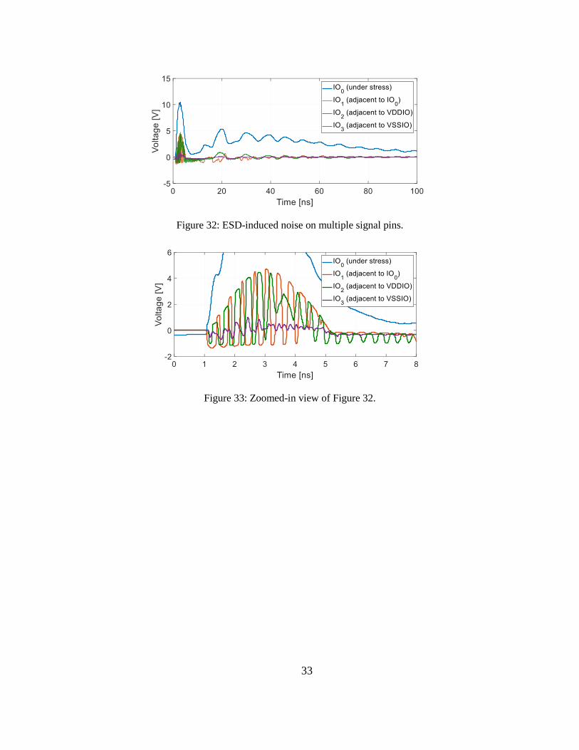
A 2 kV IEC gun zap is simulated with the gun model of Figure 17(b), assuming the EUT
is tethered. The current into IO0 and out of selected VDDIO and VSSIO pins is shown in Figure
31. For this positive discharge, most of the current flows through the top diode and returns to
ground through the VDDIO pins. The induced noise at the signal pins is shown in Figure 32,
with a zoomed-in view of the first 8 ns provided in Figure 33. Over 4 V peak-to-peak noise
appears on IO1 and IO2, while IO3 remains fairly quiet. This simulation provides information as
to which signal nets are most vulnerable to ESD-induced noise. It can be further utilized for soft
failure detection.
Figure 31: Discharge current through multiple ports.
33
Figure 32: ESD-induced noise on multiple signal pins.
Figure 33: Zoomed-in view of Figure 32.
34
CHAPTER 6: CONCLUSION
In this work, we presented modeling approaches for system-level ESD simulation that are
intended to be more accurate or informative than the commonly used methodology. We further
applied the enhanced models of the IC component and the IEC-type ESD source to a practical
system-level ESD test case.
The PDN-aware quasistatic I-V model generated through kernel regression comprehends
the impact of the circuit board PDN on the IC pin’s characteristic. The behavioral model
provides necessary information about the IC without disclosing the netlist. It has been
implemented in Verilog-A and can be simulated using a general-purpose circuit simulator.
Although it is more accurate than the conventional TLP I-V model, the enhanced quasistatic
model still lacks information about on-chip dynamics, which may induce error in transient
simulation. Therefore, it is important to identify suitable behavioral models that capture the
dynamic behavior of the IC in the future. Recurrent neural network may be a good candidate for
further investigation [19].
The IEC 61000-4-2 ESD source model is improved by better characterizing the ground
tethers with S-parameters. The model reduces the simulation error and reflects more details in
the discharge current that are affected by the tether position. However, due to the uncertainty of
the tether setup in real measurement, it is hard to achieve an exact match between simulation and
measurement.
Hybrid electromagnetic and circuit simulation is an effective approach to simulate noise
coupling inside an IC package. An IC behavioral model template that captures the multiple
return paths is proposed for use in such simulations. The simulation results show that the induced
noise is sufficiently large to cause logic errors at “internal pins” of the IC. Such simulation
provides information as to which signal nets are most vulnerable to ESD-induced noise. The
waveforms of the induced noise at the “internal pins” can be further utilized for soft failure
detection. This work remains to be completed in the future.
35
REFERENCES
[1] JEDEC, "System level ESD part I: Common misconception and recommended basic
approaches," Standard JEP-161, 2011.
[2] D. Johnsson and H. Gossner, "Study of system ESD codesign of a realistic mobile board,"
EOS/ESD Symposium, 2011.
[3] S. Bertonnaud, C. Duvvury and A. Jahanzeb, "IEC system level ESD challenges and
effective protection strategy for USB2 interface," EOS/ESD Symposium, 2012.
[4] T. Li et al., "System-level modeling for transient electrostatic discharge simulation," IEEE
Transactions on Electromagnetic Compatibility, vol. 57, no. 6, pp. 1298 - 1308, 2015.
[5] F. Escudié et al., "From quasi-static to transient system level ESD simulation: Extraction of
turn-on elements," EOS/ESD Symposium, 2016.
[6] C. Reiman et al., "Practical methodology for the extraction of SEED models," EOS/ESD
Symposium, 2015.
[7] S. Das, P. Whatmough and D. Bull, "Modeling and characterization of the system-level
power delivery network for a dual-core ARM Cortex-A57 cluster in 28nm CMOS,"
IEEE/ACM International Symposium on Low Power Electronics and Design, 2015.
[8] M. Stockinger et al., "An active MOSFET rail clamp network for component and system
level protection," EOS/ESD Symposium, 2013.
[9] E. Nadaraya, "On estimating regression," Theory of Probability & Its Applications, vol. 9,
no. 1, pp. 141-142, 1964.
[10] R. Kohavi, "A study of cross validation and bootstrap for accuracy estimation and model
selection," Proceedings of the 14th International Joint Conference on Artificial
Intelligence, 1995.
[11] N. Thomson et al., "Custom test chip for system-level ESD investigations," EOS/ESD
Symposium, 2014.
[12] IEC, "Electromagnetic compatibility (EMC) - Part 4-2: Testing and measurement
techniques - Electrostatic discharge immunity test," 2008.
[13] Y. Xiu et al., "S-parameter based modeling of system-level ESD test bed," EOS/ESD
Symposium, 2015.

36
[14] J. Xiong et al., "Enhanced IC modeling methodology for system-level ESD simulation," in
EOS/ESD Symposium, 2018.
[15] C. Ho, A. Ruehli and P. Brennan, "The modified nodal approach to network analysis,"
IEEE Transactions on Circuits and Systems, vol. 22, no. 6, pp. 504-509, 1975.
[16] T. Wang, "Modelling multistability and hysteresis in ESD clamps, memristors and other
devices," in IEEE Custom Integrated Circuits Conference, 2017.
[17] N. Thomson, Y. Xiu, and E. Rosenbaum, "Soft-failures induced by system-level ESD,"
IEEE Transactions on Device and Materials Reliability, vol. 17, no. 1, pp. 90 - 98, 2017.
[18] K. Meng, R. Mertens, and E. Rosenbaum, "Piecewise-linear model with transient
relaxation for circuit-level ESD simulation," IEEE Transactions on Device and Materials
Reliability, vol. 15, no. 3, pp. 464 - 466, 2015.
[19] Z. Chen, M. Raginsky and E. Rosenbaum, "Verilog-A compatible recurrent neural network
model for transient circuit simulation," IEEE 26th Conference on Electrical Performance
of Electronic Packaging and Systems, 2017.