enhanced power delivery pathfinding for emerging 3-d
TRANSCRIPT

IEEE TRANSACTIONS ON VERY LARGE SCALE INTEGRATION (VLSI) SYSTEMS, VOL. 29, NO. 4, APRIL 2021 591
Enhanced Power Delivery Pathfinding forEmerging 3-D Integration Technology
Andrew B. Kahng, Fellow, IEEE, Seokhyeong Kang , Member, IEEE,
Seungwon Kim, Member, IEEE, and Bangqi Xu , Graduate Student Member, IEEE
Abstract— In advanced technology nodes, emerging 3-Dintegration technology is a promising “More Than Moore” leverfor continued scaling of system capability and value. In the3-D integrated circuit (3-D IC) implementation, the power deliv-ery network (PDN) is crucial to meeting design specifications.However, determining the optimal PDN design is nontrivial.On the one hand, to meet the voltage (IR) drop requirement,a denser power mesh is desired. On the other hand, to meet thetiming requirement, more routing resource is needed for signalrouting. Moreover, additional competition between signal routingand power routing is caused by intertier vertical interconnects in3-D IC. In this article, we propose a power delivery pathfindingmethodology for emerging 3-D integration, which seeks to identifya “near-optimal” (or, very high quality) PDN for a given BEOLstack, vertical interconnection, and PDN specification. Comparedwith previous works, our methodology can explore richer solutionspaces as it supports different PDN layer combinations and PDNlayer configurations. We develop models for routability and worstIR drop to help reduce iterations between PDN design and circuitdesign in 3-D IC implementation. We present validations anddemonstrate improvement in IR drop and routability with realdesign blocks in 28- and 14-nm foundry technology nodes.
Index Terms— 3-D integration, voltage (IR) drop prediction,power delivery, routability analysis, system pathfinding.
I. INTRODUCTION
MODERN very-large-scale integration technology hasenabled higher system performance and efficient
power management based on advanced transistor technology.
Manuscript received August 1, 2020; revised October 26, 2020; acceptedNovember 15, 2020. Date of publication December 21, 2020; date of currentversion April 1, 2021. This work was supported in part by Qualcomm, in partby Samsung, in part by NXP Semiconductors, in part by Mentor Graphics,in part by Defense Advanced Research Projects Agency (DARPA) under GrantHR0011-18-2-0032, in part by NSF under Grant CCF-1564302, and in partby the C-DEN Center. (Seungwon Kim and Bangqi Xu contributed equally tothis work.) (Corresponding author: Bangqi Xu.)
Andrew B. Kahng is with the Department of Computer Science andEngineering, University of California at San Diego, La Jolla, CA 92093USA, and also with the Department of Electrical and Computer Engineering,University of California at San Diego, La Jolla, CA 92093 USA (e-mail:[email protected]).
Seokhyeong Kang is with the Department of Electrical Engineering,Pohang University of Science and Technology (POSTECH), Pohang 37673,South Korea (e-mail: [email protected]).
Seungwon Kim is with the Department of Computer Science and Engineer-ing, University of California at San Diego, La Jolla, CA 92093 USA (e-mail:[email protected]).
Bangqi Xu is with the Department of Electrical and Computer Engineering,University of California at San Diego, La Jolla, CA 92093 USA (e-mail:[email protected]).
Color versions of one or more figures in this article are available athttps://doi.org/10.1109/TVLSI.2020.3041665.
Digital Object Identifier 10.1109/TVLSI.2020.3041665
Fig. 1. Two integration technologies for foundry-driven 3-D IC. (a) WoWintegration. (b) D2W integration.
With foundry 7-nm products reaching high-volume production,only a few feasible technology nodes remain to potentiallydeliver power, performance, area, and cost (PPAC) benefitsfrom the transistor, cell architecture, and lateral scaling. 3-Dintegrated circuit (3-D IC) stacking techniques are receivingattention as a promising solution to continue Moore’s Lawfor future scaling of integration, area footprint, and designperformance/power envelope.
3-D IC stacking technologies have historically been drivenfrom two directions: the packaging industry and the foundryindustry. Conventional packaging-driven 3-D IC technologiesbased on through-silicon vias (TSVs) have limitations to thehigh vertical integration density at the die level due to the sizeand pitch of the TSV structure [1]. Recent advanced intertiervertical interconnect (VI) technology has led to the emergenceof multiple foundry-driven 3-D IC technologies to achievesignificant PPAC benefits; these include high-precision face-to-face (F2F) wafer-on-wafer (WoW) and die-to-wafer (D2W)stacking, as shown in Fig. 1 [13], [34]. WoW technologyfocuses more on power, performance, and area improvements,while D2W technology seeks more cost-effective integrationmethods to enhance system-level power and performance, e.g.,for memory-on-logic, single-chip solutions. WoW faces twokey limitations compared with D2W technology: 1) the samearea constraint for top and bottom dies limits partitioningscenarios and 2) overall low yield. On the other hand, D2Wtechnology has achieved yield improvements with prebondingtesting for existing 2-D IPs. Therefore, existing 2-D EDAtools can be used to perform realistic experiments for D2Wstacking. In addition, D2W facilitates the integration of aheterogeneous 3-D IC into multiple dies (e.g., a large bottomdie and variously sized smaller top dies). With this process-friendly approach coupled with relatively high integrationdensity, D2W technology has become a practical solution tocope with 2-D scaling challenges.
A power delivery network (PDN) in the back end ofline (BEOL) has a direct impact on the reliability and function-ality of the product design. Determining high-quality PDNswith the increasing power density and design complexity ischallenging even in 2-D ICs. The challenges are exacerbated
1063-8210 © 2020 IEEE. Personal use is permitted, but republication/redistribution requires IEEE permission.See https://www.ieee.org/publications/rights/index.html for more information.
Authorized licensed use limited to: Univ of Calif San Diego. Downloaded on April 01,2021 at 03:55:55 UTC from IEEE Xplore. Restrictions apply.

592 IEEE TRANSACTIONS ON VERY LARGE SCALE INTEGRATION (VLSI) SYSTEMS, VOL. 29, NO. 4, APRIL 2021
Fig. 2. Brief example of PDN design from the lowest layer to the toplayer in BEOL. (a) In the 3-D IC, when using an optimal PDN structureof 2-D IC, routing congestion occurs due to lower routability in the highermetal layers. A design that is too pessimistic about routing congestion usesless PDN and, thus, has a large IR drop. (b) Our proposed “one-shot”pathfinding methodology obtains near-optimal PDN parameters (i.e., yieldingbest routability while meeting the IR drop requirement) with a one-time effortfor each tier.
in 3-D ICs with additional resistance between the powersupply and transistors in different tiers. In addition, feasibledesign solutions are limited because signal and power/groundrouting must be passed through the intertier VIs. Smallersizes of intertier VIs can make new integration feasible,but the higher resistance adversely affects the PDN quality[36], [37]. To achieve robust functionality, 3-D IC designsmust mitigate and balance these PDN-related challenges.Fig. 2(a) illustrates a conventional PDN design flow for 3-DIC, where designers iteratively explore a large PDN designspace to reach a balance between voltage (IR) drop androutability. However, this process takes a considerable portionof the design cycle. To reduce the turnaround time in 3-DIC design, ideally, a PDN pathfinding flow in 3-D IC wouldbe capable of delivering a near-optimal PDN design withoutany iterations as illustrated in Fig. 2(b). This demands anefficient, accurate design space exploration (also known aspathfinding) methodology that—given various technology- anddesign-dependent parameters—can quickly provide quality ofresult (QoR) tradeoffs of various PDN solutions.
Our work builds on the power delivery pathfinding approachof [16], in which a fixed combination of BEOL layers isused for power delivery. Compared with [16], we propose anefficient two-stage pathfinding methodology for PDN designof emerging F2F 3-D designs that explore a larger designsolution space, including various PDN layer combinations.In the literature and industry, finding good PDN designs isdifficult largely due to the large solution space of PDN designsand the long turnaround time for PDN evaluation. With oursolutions, near-optimal PDN designs can be found with modelsbased on a relatively small set of data points from smallartificial designs. In the first stage, we create sensitivity graphsthat consider the IR drop and routability tradeoff and apply theshortest path algorithm to obtain a PDN layer combinationwith minimized cost. In the second stage, based on the layercombination obtained from the first stage, we build an IRdrop model to predict the worst IR (WIR) drop of a givenPDN configuration. To comprehend the effect of a givenPDN solution on the overall design QoR, we also developa routability model that predicts the routability of a designgiven a PDN configuration.
Putting the first- and second-stage elements together, ourpathfinding methodology starts by identifying the best PDN
layer combination considering both WIR and routability. Forthe best PDN layer combination, we then filter out PDNconfigurations based on a given design’s prescribed WIRlimits. Finally, the routability model is used to identify theWIR-feasible PDN configuration(s) that offer the best routabil-ity. We, thus, obtain a high-quality PDN solution that is “near-optimal” (to the extent that we have been able to make exhaus-tive enumeration-based experimental confirmations) in thesense of both predicted WIR and estimated routability withinour modeled PDN design space. Our PDN solution approachoffers direct benefits to design QoR and ease of implementa-tion. The main contributions of our work are as follows.
1) We propose a novel interface to properly combine IRdrop analysis of PDN configurations and the correspond-ing impact on routability.1
2) We study the impact of VI density (VIdensity) on designroutability and build a VI-aware routability model.
3) We develop IR-drop and routability sensitivity graphsto obtain a best PDN layer combination given a set ofIR-drop and routability weights.
4) On foundry 28-nm designs, we demonstrate that ourpathfinding methodology identifies high-quality PDNdesigns compared with a reference industry PDN design.
5) We further confirm that our pathfinding methodologyimproves over an industrial PDN reference solution infoundry 14-nm technology.
6) To the best of our knowledge, we are the first to proposea pathfinding methodology that explores both PDNlayer combination and per-layer PDN configuration toidentify high-quality solutions for F2F 3-D designs.
The remainder of this article is organized as follows.Section II provides an overview of related works in theliterature. Section III introduces our PDN pathfinding method-ology. Section IV describes our PDN layer combinationpathfinding (Stage 1), and Section V shows the experimentalsetup and results for this PDN layer combination pathfinding.Sections VI and VII, respectively, describe our PDN layerconfiguration pathfinding (Stage 2) and experimental results.We validate our overall two-stage PDN pathfinding flow inSection VIII. In Section IX, we extend our proposed methodol-ogy to 14-nm foundry technology. Section X gives conclusionsand directions for ongoing works.
II. RELATED WORKS
In this section, we review previous works in the literature.We classify relevant previous works into three categories:1) 3-D IC implementation methodology; 2) PDN designmethodology; and 3) routability modeling.
A. 3-D IC Design Implementation Methodology
Several design methodologies using existing commercial2-D CAD tools have been proposed for physical implemen-tation of gate-level 3-D ICs [8], [19], [20], [22], and [24].The Shrunk2D (S2D) flow [22], [24] performs gate-level3-D IC implementation, while the subsequent Cascade2D flow
1Note that we do not attempt PDN pathfinding that considers dynamic IRdroop. This remains a “holy grail” that depends on the evolution of techniques,such as what we propose here and determining proper simulation vectors.Also, while our work aligns with goals, such as PDN pathfinding for largeSoC designs, we focus on the 3-D IC context and its unique complexities, at ablock scale (and we do not have access to large SoC designs and collateraldata).
Authorized licensed use limited to: Univ of Calif San Diego. Downloaded on April 01,2021 at 03:55:55 UTC from IEEE Xplore. Restrictions apply.

KAHNG et al.: ENHANCED POWER DELIVERY PATHFINDING FOR EMERGING 3-D INTEGRATION TECHNOLOGY 593
implements both gate- and block-level monolithic 3-D ICs [8].Recently, a commercial-quality F2F-bonded 3-D IC imple-mentation flow Compact-2D (C2D) has been proposed [20].We note that these works on 3-D IC implementation leaveopen the issue of interactions between power delivery androutability.
B. PDN Design MethodologyPower delivery in gate-level 3-D ICs is considered in [23],
which proposes a PDN-centered tier-partitioning techniquethat comprehends the IR drop versus thermal tradeoff inmonolithic 3-D IC. Samal et al. [29] analyze full-chip impactof PDN designs in monolithic 3-D ICs. Optimized 3-DPDN design configurations (in six categories) are comparedacross power, performance, IR drop, and wirelength metricsin different technology nodes. However, design-specific PDNchoices at the “Pareto frontier” of IR drop versus routabilityare not addressed, as this would require exploration of PDNstructures with degrees of freedom on each metal layer.Chang et al. [9] develop a system-level PDN model, alongwith static and dynamic frequency- and time-domain analyses.The 2-D and 3-D ICs with extracted equivalent RLC par-asitics are compared using a single-baseline PDN structure.The focus is on dynamic rail analysis with frequency-relatedenvironmental differences (e.g., decap insertion) rather thanPDN optimization. Chang et al. [7], Chhabria et al. [12],and Kahng et al. [16] propose model-based power deliverypathfinding methodology that explores PDN design solutionspace for a given, fixed PDN layer combination (e.g., M2, M3,M4, M7, and M8). With these approaches, the exploration ofdifferent PDN layer combinations would require much moredata for modeling and may encounter scalability challenges.Furthermore, vertical connections are not considered as theseworks are limited to the 2-D IC context.
C. Routability ModelingNumerous techniques have been devised toward estimation
of signal routing congestion in placement and global routingstages [11], [18], [21], [31]. Various methods, respectively,apply Rent’s rule to estimate the wirelength distributionof a region [32], estimate congestion by analysis of pindensities [3] or Steiner trees [28], or achieve bounding box-aware per-net wirelength estimation [4]. Machine learning-based routing congestion prediction models have also beenproposed. Qi et al. [27] apply supervised learning to predictdetailed routing violation and utilization in the global routingstage via multivariate adaptive regression splines (MARS).Zhou et al. [33] propose a machine learning model thatpredicts DRC violations from placement and global routingdata. Chan et al. [5] extract hotspot features to identify gcellswith DRC violations.
This work requires routability estimation that considers bothBEOL stacks (including PDN and technology rules) alongwith given placement. Thus, in the following, we employ theroutability characterization methodology of “PROBE” [15],which affords a ranking of BEOL stack options according totheir intrinsic routing capacities.2
2 Kahng et al. [15] note several challenges associated with studies of realdesign blocks, which can have: 1) large cell instance counts; 2) large variancein cell sizes; and 3) nonuniformity in net topologies. Our PDN pathfindingproblem has these same challenges and additional impacts from TSV andVI connections. However, as noted, we confirm the robustness of our proposedmethodology with real design blocks in two different foundry technologies.
Additional works have studied the issue of vertical cuts(interconnect demands) in gate-level 3-D IC implementation,e.g., attempting to maximize the benefits of 3-D ICs byincreasing the number of monolithic intertier vias (MIVs) orF2F VIs [20], [22]. Peng et al. [26] note that, as the num-ber of vertical cuts increases, interdie coupling capacitanceincreases, significantly affecting power and signal integrity inF2F bonded ICs.
D. Summary
From the above, we see that, while previous works on 3-DIC implementation have illuminated many aspects of parti-tioning, place-and-route, and power delivery, typically, only avery limited PDN solution space is considered. The need forPDN pathfinding in 3-D IC arises because power/ground (PG)delivery is far from “free”: in 3-D ICs, there are TSV androutability impacts, as well as a need for the PDN solution tosupport the delivery of PG and signal through intertier VIs.The number of VIs is a significant determinant of power andsignal integrity, in light of routing congestion and IR drop.This is in contrast to PDNs in 2-D ICs that are generally lesssensitive to signal routing congestion on upper metal layers.3
Our work attempts to close this gap by explicitly consideringboth IR drop and routability.
III. METHODOLOGY
In this section, we first generalize the PDN pathfindingproblem presented in [16] and then describe our approach forPDN pathfinding methodology considering both PDN layercombination and PDN layer configuration.
1) PDN Pathfinding Problem: Given a mesh-like placementwith VI locations, provide an optimized PDN designconsidering IR and routability.
2) Inputs: Mesh-like placement, VI locations, and BEOLstack.
3) Output: PDN with optimized IR and routability.4) Constraints: Technology design rules.
A. Preliminaries
We divide the overall PDN pathfinding problem into twosubproblems that are sequentially solved in the proposedtwo-stage PDN pathfinding methodology. We define the twostages for solving the two subproblems as follows.
1) PDN layer combination pathfinding focuses on thechoices of metal layers in a BEOL stack that is usedfor PG metal stripes (e.g., M2-M3-M4-M7-M8).
2) PDN layer configuration pathfinding focuses on thedetailed usage of routing resources (i.e., PDN density)of each metal layer for a given PDN layer combination(e.g., a set of PG stripe {width, spacing, pitch} configu-rations for all metal layers in a PDN layer combination).
For PDN layer combination pathfinding, in order to qual-itatively provide guidance on the detailed usage of routingresources, we define a usage corner as a tuple of {width,spacing, pitch}.4 For PDN layer configuration pathfinding,
3If the total number of VIs is high relative to the total number of nets (i.e.,a high #VIs-to-#nets ratio), this implies that the number of 3-D nets traversingthrough the VIs located on the top metal layer is also relatively high. Theimpact of these VIs (which are induced by the design’s partition across tiers)must be considered in the 3-D IC PDN design.
4In Section IV, we define three typical usage corners (i.e., min, base, andmax). A finer granularity of usage corners can provide more detailed guidancefor PDN layer configuration pathfinding.
Authorized licensed use limited to: Univ of Calif San Diego. Downloaded on April 01,2021 at 03:55:55 UTC from IEEE Xplore. Restrictions apply.

594 IEEE TRANSACTIONS ON VERY LARGE SCALE INTEGRATION (VLSI) SYSTEMS, VOL. 29, NO. 4, APRIL 2021
Fig. 3. Illustration of circuit design-independent PDN design knobs.
TABLE I
PDN DESIGN KNOBS
we define PDN design knobs to explore the PDN layerconfiguration solution space. Table I shows the PDN designknobs that we consider. Circuit design-independent knobsinclude width, space, and pitch size of metal stripe, as shownin Fig. 3. Combinations of these knobs must satisfy the designrule constraints of the given technology. For a given 3-D ICdesign, the circuit design-dependent knobs include the numberof cell instances, row utilization, and VIdensity.
B. Routability Measurement
While WIR can be directly measured by a power analy-sis tool, measurement of routability is less straightforward.In the context of 3-D IC, with consideration of TSV andVI effects, routability measurement becomes even more chal-lenging. We apply the core technique of PROBE [15] toobtain an intrinsic measure of routability of a given PDNdesign, in terms of the so-called “K threshold” (Kth) metric,based on a mesh-like placement. We construct a mesh-likeplacement, as illustrated in Fig. 4(a). A mesh-like placementuniformly arranges netlists in a Wdie × Hdie floorplan, whereHdie = Mr × Hgate and Wdie = Mc × Wgate/U according to themesh topology. Mr is the number of rows indexed by p, andMc is the number of columns indexed by q . Wgate and Hgate arethe width and height of a given cell, respectively, and U is apredefined placement (row) utilization. For a mesh-like place-ment, as shown in Fig. 4(a), each pin of a given instance isinitially connected to its neighboring instances, and originally,there are zero (or very few) design rule violations after routing.
The PROBE methodology iteratively swaps the placementlocations of random pairs of neighboring instances. This pro-gressive “tangling” gradually degrades the placement, increas-ing congestion until, eventually, the perturbed placementbecomes unroutable (i.e., the number of postroute design ruleviolations exceeds a predefined threshold).5 The number ofneighbor swaps (normalized to total instance count) beforerouting failure occurs is called the K threshold (Kth). We usea three-input AOI cell as the basis for the starting mesh-like placement, with inputs and output of each cell beingconnected, as shown in Fig. 4.6
5Following [15], we define routing failure as #DRVs > 150.6Note that, for training data collection, the mesh-like placement enables
the fine-grained increase of routing difficulty with decent runtime scalabilitycompared with placement perturbation and routing for real design blocks.
Fig. 4. Illustration of (a) mesh-like placement as in [15] and (b) our 3-Dmesh-like placement with VIs (on top metal layer).
A robust PDN design can potentially consume considerablerouting resources as it satisfies the WIR constraint; this,in turn, worsens routing congestion in surrounding areas.When comparing PDN designs, a higher Kth value implies thata given PDN design has better routability, i.e., more routingcapacity. According to [15], the rank ordering of BEOLrouting capacities, based on mesh-like placement, is stableand consistent across different designs. In this work, we makethe key observation that different PDN designs implementedin a BEOL stack are equivalent to variants of the originalBEOL stack with reduced routing capacities. Following thisobservation, we can measure the routability of a PDN for agiven BEOL stack, and the rank ordering of routabilities acrossPDNs can be generalized and applied to different designs.To understand the impact of VIs on routability of a givenPDN in the 3-D IC context, we extend the mesh-like placementwith connections from cell pins to VI pins on the top metallayer, as shown in Fig. 4(b). We fix the locations of VI pinsduring the random swapping of neighboring cells. We usethe parameter VIdensity (see Table I) to reflect that the impactof VI on relative routability (of a given BEOL stack plusPDN) is independent of the design size. The number of VIs isdetermined by VIdensity ×#nets. The VIs are placed on the topmetal, and VIs do not overlap the PDN.7 Each VI is connectedto the net of the nearest cell output pin.
C. F2F Mesh-Like Placement Setup
Unlike the 2-D mesh-like placement used in PROBE [15],routability measurement in 3-D IC must comprehend theunique aspects of vertical interconnection, including TSVsand intertier connections. Therefore, in our setup of mesh-likeplacement for the F2F case, we place TSVs on the bottomtier as both placement and routing blockages. Following themethodology of such works, as in [22], we place I/O ports onthe top routing layer to capture the behavior of VIs for intertierconnections. Fig. 5(a) illustrates the cross section view of F2Fstacking with TSV, and Fig. 5(b) illustrates our implementationfor routability and WIR experiments. In order to simulate the3-D F2F stacking structure with available 2-D EDA tools,we replace the connections between PDN TSVs and top-layerPDN of the top tier with fictitious metal stripes and vias withvery low resistance, such that the top-layer PDNs from bothtiers are virtually shorted.8
Fig. 6(a) illustrates the top view of F2F stacking with TSV,and Fig. 6(b) illustrates our implementation for F2F mesh-likeplacement with PDN. We use a staggered TSV allocation with
7Note that, to implement routing by a commercial 2-D P&R tool in ourexperiments, the VIs in the routability model are placed as I/O pins. Thistechnique has been used in previous works, such as [22].
8We recognize that the setup in Fig. 5(a) is not identical to the setupin Fig. 5(b), and that different current distributions will result. However,our separate studies confirm that such differences are small, do not affectthe dominance of bottom-tier WIR, and do not qualitatively change ourconclusions.
Authorized licensed use limited to: Univ of Calif San Diego. Downloaded on April 01,2021 at 03:55:55 UTC from IEEE Xplore. Restrictions apply.

KAHNG et al.: ENHANCED POWER DELIVERY PATHFINDING FOR EMERGING 3-D INTEGRATION TECHNOLOGY 595
Fig. 5. Cross section view illustrations of (a) F2F stacking with TSV and(b) our experimental implementation. Physical connections from PDN TSVsto top-tier PDN are replaced by fictitious metal stripes and vias with verylow resistance such that the top-most PDN layers from both tiers are virtuallyshorted. VIs are replaced with I/O ports to mimic intertier connection.
Fig. 6. Top view illustrations of (a) mesh-like placement with TSVs and(b) mesh-like placement with PDN overlay.
TSV size of 2.4 × 2.4 μm2, an array pitch size of 40 μm,and offset between VDD and VSS of 10 μm in this work.We perform routability and WIR experiments with the imple-mentation described in Fig. 5(b) where both the routabilityand WIR characteristics of the design are preserved comparedwith the F2F stacking case. In the following, the routabilitystudies are performed considering the TSVs unless otherwisespecified.
D. Overall Flow
As mentioned in Section II, previous works have mainlyfocused on exploring PDN design solution space when thePDN layer combination is fixed due to scalability limitations.To achieve a power delivery pathfinding flow that exploresa solution space, including both PDN layer combinationand PDN layer configuration, we propose a two-stage PDNpathfinding methodology.
Fig. 7 illustrates the two stages of our methodology.In Stage 1, we formulate the PDN layer combination pathfind-ing problem as a shortest-path computation in a sensitivitygraph, which determines the best layer combination. We intro-duce the routability-IR tradeoff factor α to modulate thebalance of routing resource usage between PDN and signalrouting. In Stage 2, based on the layer combination obtainedfrom Stage 1, we develop and apply WIR and routability
Fig. 7. Two-stage PDN pathfinding flow that gives the optimized PDNlayer combination and per-layer PDN configuration considering both WIRrequirement and routability requirement.
models to filter and rank possible PDN layer configurations,so as to obtain the most promising PDN design for givenBEOL stack and WIR requirements. We validate our two-stagePDN pathfinding flow in Section VIII.
IV. STAGE 1: PDN LAYER COMBINATION PATHFINDING
In this section, we describe the problem statement and ourshortest-path-based formulation for PDN layer combinationpathfinding problem. As mentioned earlier, there is an obvi-ous tradeoff between PDN quality and routability. Therefore,we introduce a routability-IR tradeoff factor α to modulate thebalance between routability and WIR metrics. The followingequation shows the cost function that we use in PDN layercombination pathfinding: a weighted sum of routability (i.e.,Kth) and WIR (i.e., mV):
cost = α · costKth + (1 − α) · costIR. (1)
We validate our shortest-path-based PDN layer combinationpathfinding flow in Section V-B.
1) PDN Layer Combination Pathfinding Problem: For amesh-like placement, a BEOL stack, and routability-IR tradeoff factor, find the PDN layer combination thatgives the minimum cost.
2) Inputs: Mesh-like placement, baseline PDN design,routability-IR tradeoff factor α, and PDN resource usagecorners.
3) Output: PDN layer combination that gives the minimumcost along with resource usage guidance for each metallayer.
For a given BEOL stack with n metal layers and mPDN resource usage corners, our goal is to find the PDNlayer combination that gives the minimum weighted sum ofroutability cost and IR cost from a sensitivity graph. Thesensitivity graph, for which we require O(m ·n) experiments toobtain the sensitivity (i.e., cost) of each edge, is able to predictan overall solution space that requires O(mn) experiments toobtain ground-truth data.
A. Sensitivity Graph
Similar in spirit to [2], we explore the possibility of lever-aging a superposition assumption (i.e., empirical property)for each of routability and WIR of PDN for a given BEOLstack. Without loss of generality, we use Fig. 8 to illustratethe process of sensitivity graph construction with a BEOLstack with eight metal layers and three PDN resource usagecorners.
Authorized licensed use limited to: Univ of Calif San Diego. Downloaded on April 01,2021 at 03:55:55 UTC from IEEE Xplore. Restrictions apply.

596 IEEE TRANSACTIONS ON VERY LARGE SCALE INTEGRATION (VLSI) SYSTEMS, VOL. 29, NO. 4, APRIL 2021
Fig. 8. Sensitivity graph of a BEOL stack of eight metal layers for PDN.
Each vertex in the sensitivity graph only serves for con-nectivity purposes and does not have physical meaning.Each edge in the sensitivity graph represents a usage corner(i.e., min, base, or max) of a metal layer if the correspondingmetal layer is used for PDN. For example, M3min indicatesminimum routing resource usage for PDN on M3, and M5jumpindicates that PDN does not use M3 or M4. Each directedpath from node N2 to node N9 represents a valid PDN. Forexample, the path consisting of edges {M2base − M3base −M4base − M5base − M6base − M7base − M8base} represents ourbaseline PDN design. Note that the purpose of the baselinePDN design is to provide baseline Kth and WIR values foredge cost calibration.
B. Edge Cost Characterization and Shortest Path
From the baseline PDN design, we perform one of thefollowing operations at a time to obtain a variant PDN layercombination and calculate the routability and WIR costs ofeach edge in the graph.
1) Single-Layer PDN Resource Tuning: Replace an edgethat belongs to baseline PDN with min or max edge.
2) PDN Layer Skipping: Replace two consecutive edges inthe baseline PDN with a skip edge.
For each variant PDN layer combination, we performroutability analysis (respectively, IR drop analysis) and cal-culate the difference from baseline PDN layer combinationanalysis result to obtain edge routability cost (respectively,WIR cost). We normalize the routability cost and WIR costusing
x̄ = (x − μ)/σ (2)
where μ represents the mean value of all raw data and σrepresents the standard deviation of all data for routability andWIR, respectively. Note that, for routability cost, we take thenegative normalized value of the difference in Kth since higherKth indicates better routability, which should correspond to alower cost in the sensitivity graph.
For a given routability-IR tradeoff factor α, we apply(1) to calculate the cost for each edge. We then apply theshortest-path algorithm to obtain the shortest path from nodeN2 to node N9, which represents the PDN layer combina-tion that has the minimum weighted sum of routability andWIR costs.
V. EXPERIMENT AND VALIDATION OF PDNLAYER COMBINATION PATHFINDING
In this section, we describe our experimental setup and theresults of the PDN layer combination pathfinding.
We perform experiments with an eight-track 28-nm FDSOIfoundry enablement with a ten-metal-layer BEOL stack. Therow utilization is determined by the number of availablecell rows. For example, eight vertical tracks on a cell and
Fig. 9. Illustration of PG via array generation strategies. (a) Continuous viaarray. (b) Split via array.
TABLE II
REFERENCE DESIGN OF PDN FOR 28-nm FDSOI DESIGN ANDPDN LAYER CONFIGURATIONS FOR SCALABILITY STUDY
three vertical tracks of white space imply a row utilizationof 0.727.9 For the PROBE-like routability study, we performplace-and-route using Cadence Innovus Implementation Sys-tem v17.10 [39]. To comprehend the impact of TSVs onroutability in 3-D IC implementation, we use TSVs as routingblockages during the PROBE-like routability study. Note thatthe PDN layer combinations considered in this work can haveM3 PG stripes connected to M8 PG stripes directly using PGvias. In order to avoid blocking an excessive amount of routingresources between two nonneighboring routing layers, we splitthe generated PG vias, as shown in Fig. 9. Hence, the PDNsin this work are different from the PDNs in [16] even if theparameters are the same.
For the WIR study, we perform static IR analysis usingANSYS RedHawk v15.1.1 [42]. To capture the impact ofTSVs on IR drop in 3-D IC implementation, TSVs aretreated as blockages when we construct the PDNs, andthe power is supplied through TSVs and then redistrib-uted from the top metal layer, as illustrated in Fig. 5(b).Table II shows the reference design that we use for ourexperiments.10
A. Scalability Study
We study the scalability of our approach by varying designsize as described. We perform routability analysis using vari-ations of the reference PDN design.11 We sweep the numberof cells from 25k to 100k with a step size of 25k for a fixedutilization. A total of 24 distinct PDNs are enumerated byvarying one parameter at a time, between 75% (small) and
9For ease of use, the values of the following utilizations are rounded to thefirst decimal place.
10For the feasibility of our determining the ground truth for all PDNcombinations, we set up a reference with a low top-most layer.
11WIR in 3-D IC depends on specific boundary conditions. We experimen-tally confirm that there is no obvious correlation between #Instances and WIRfor a given utilization.
Authorized licensed use limited to: Univ of Calif San Diego. Downloaded on April 01,2021 at 03:55:55 UTC from IEEE Xplore. Restrictions apply.

KAHNG et al.: ENHANCED POWER DELIVERY PATHFINDING FOR EMERGING 3-D INTEGRATION TECHNOLOGY 597
Fig. 10. Routability (Kth) versus #instances for 24 PDN variants derivedfrom the reference PDN.
175% (big) of the corresponding value used in the referencePDN, as shown in Table II.
Fig. 10 shows the impact of design size (in terms of#instances) on routability (i.e., Kth). We can observe thatroutability decreases as we increase the design size. Note that,as expected, none of the 24 PDN variants from the referencePDN changes routability dramatically for a given design size.Although there is a change in the absolute value of Kth whendesign size changes (as explained in [15]), the routability rankordering of PDN designs is independent of design size. Basedon our empirical observation of this stability under scaling,we fix the number of instances at 25k for all the experimentsreported in the following.
B. Sensitivity-Based PDN Layer Combination Pathfinding
To validate our approach, we perform experiments to obtainthe ground-truth data of all PDN layer combinations definedby PDN layer usage corners for each metal layer. We assessthe accuracy of our sensitivity-based PDN layer combinationpathfinding approach by comparing the rank ordering of path-based cost and the rank ordering from ground-truth data.To assess the impact of routability-IR tradeoff factor α on ourPDN layer combination pathfinding approach, we use differentα values and perform the rank ordering comparison.
1) Routability and WIR Sensitivity Graph Construction:As mentioned in Section IV, we measure the impact of addingPG stripes on a certain metal layer to build a sensitivity graphcomprehending both routability and WIR. We apply single-layer PDN resource tuning (i.e., switching between PDN layerusage corners) or 2) PDN layer skipping to obtain PDNlayer combination variants. Compared with a baseline PDNlayer combination (i.e., {M2base − M3base − M4base − M5base −M6base − M7base − M8base} path in Fig. 8), we measure thedifference in routability (in terms of Kth value) and WIRbetween the baseline PDN layer combination and PDN layercombination variants. Table III shows the various PDN usagecorners that we consider in this work. The minimum PDN isset to 75% of the width of the base PDN, and the spacing andthe set-to-set pitch are set to 175%.
Tables IV and V show the raw/normalized routability andWIR cost, respectively. As mentioned in Section IV, we takethe negative value of normalized routability cost for weightedsum edge cost calculation for a given routability-IR tradeofffactor α. We illustrate the ranges of WIR and routabilitysensitivity for corner cases (i.e., min and max for eachlayer) in Fig. 11. We can observe that, for each metal layer,
TABLE III
PDN CONFIGURATIONS FOR EACH METAL LAYER WHICH USE MIN,BASE, AND MAX RESOURCES. PDN DENSITY IS CALCULATED
AS THE NUMBER OF BLOCKED TRACKS FROM THE TOTAL
NUMBER OF TRACKS PER LAYER
TABLE IV
RAW AND NORMALIZED ROUTABILITY EDGE SENSITIVITY COST
TABLE V
RAW AND NORMALIZED IR EDGE SENSITIVITY COST
the sensitivity values of the baseline PDN design for both WIRand routability lie between the corresponding values of minand max PDN, as expected.
2) Sensitivity-Based PDN Layer Combination Pathfinding:To assess the accuracy of our graph-based method, we mea-sure all possible PDN layer combinations in the graph toobtain ground-truth WIR and routability values. For a givenpair of WIR and routability weights, we compare the rankordering of all layer combinations between the graph-basedresult and the ground truth. Fig. 12 shows the rank orderingcomparison between the graph-based method and groundtruth. We achieve a Spearman’s coefficient of 0.96, whichsuggests that the graph-based method can accurately capturethe tradeoff between WIR and routability for various layercombinations.
Authorized licensed use limited to: Univ of Calif San Diego. Downloaded on April 01,2021 at 03:55:55 UTC from IEEE Xplore. Restrictions apply.

598 IEEE TRANSACTIONS ON VERY LARGE SCALE INTEGRATION (VLSI) SYSTEMS, VOL. 29, NO. 4, APRIL 2021
Fig. 11. IR and routability sensitivity analysis results for min/base/maxconfigurations for each layer of the PDN. (a) WIR sensitivity. (b) Routabilitysensitivity.
Fig. 12. Correlation results between graph-based method and ground truthfor (a) WIR and (b) routability.
3) Impact of α on Rank Ordering: We use differentroutability-IR tradeoff factor α values to assess the impactof α on rank ordering. We use three α values {0.2, 0.5, 0.8}to represent different tradeoffs between routability and WIR.For each α value, we perform experiments with a totalof 1080 PDNs. We summarize the breakdown of PDNs fromdifferent scenarios as follows.
1) Using All Layers: 3#PDNLayers = 729.2) Skipping Two Layers: 3#PDNLayers−2 × #skipCase =
34 × 4 = 324.3) Skipping Four Layers: 3#PDNLayers−4 × #skipCase =
32 × 3 = 27.Fig. 13(a) and (b) shows the graph-based approach and
ground truth of tradeoff between routability and WIR withthe three α values, respectively. We highlight the Pareto curvefrom the graph-based approach in both Fig. 13(a) and (b).We can observe that the Pareto curve obtained from the graph-based approach fits the ground-truth tradeoff, which providesconfirmation of the effectiveness of our approach.
VI. STAGE 2: PDN LAYER CONFIGURATION PATHFINDING
In this section, we describe the problem statement and ourmodel-based flow for the PDN layer configuration pathfindingproblem given a PDN layer combination. For a given PDNlayer combination, we define the PDN layer configurationpathfinding problem as follows.
1) PDN Layer Configuration Pathfinding Problem: Givena mesh-like placement, VI locations, and a PDN layercombination, provide a PDN design that meets the WIRlimit with best routability.
2) Inputs: Mesh-like placement, VI locations, and PDNlayer combination.
3) Output: PDN with best routability meeting the WIRlimit.
4) Constraints: WIR and technology design rules.
Fig. 13. Illustration of tradeoff between routability and WIR withα = {0.2, 0.5, 0.8} for (a) graph-based approach and (b) ground truth. ThePareto curve in (a) and (b) are both from the graph-based approach.
A. WIR and Routability Modeling
Fig. 14 illustrates the WIR and routability modeling flow.For a collection of PDN candidates, we perform static IRanalysis on a mesh-like placement. We sweep the circuitdesign-independent knobs (i.e., width, spacing, and pitch ofPG stripes) to generate a training data set of PDN layerconfigurations and obtain their corresponding WIR values.Based on the WIR values in the data set, we train a WIRmodel and use the model to predict the WIR for different PDNlayer configurations. Fig. 14(a) illustrates the WIR modelingflow. Similar to WIR modeling flow, we build a routabilitymodel based on Kth values from the PDN layer configurationcandidates. Fig. 14(b) illustrates the routability modeling flow.We perform PROBE-like routability analysis [15] to collectKth data for various PDN layer configuration candidates.Besides the PDN variables including metal width, spacing,and pitch, we also consider utilization and VIdensity in theroutability model, so as to comprehend the competition forrouting resources between PDN and signal routing.
We use learning-based algorithms, such as the ordinaryleast-squares method (multivariable linear regression), andMARS [14], to build regression models for both WIR androutability. By combining several models (multivariable linearregression and MARS), we achieve a hybrid surrogate modelto assess the WIR and routability of PDN layer configurations.Model validations are discussed in Section VII-C.
B. Model-Based PDN Layer Configuration Pathfinding
For a given PDN layer combination, PDN layer configura-tions are enumerated honoring technology constraints (width,space, and pitch) for all stripes on all layers. We use the WIRmodel to prune the PDN solution space according to the WIRrequirement. For the enumerated PDN layer configurations,we apply the WIR model to predict their respective WIR
Authorized licensed use limited to: Univ of Calif San Diego. Downloaded on April 01,2021 at 03:55:55 UTC from IEEE Xplore. Restrictions apply.

KAHNG et al.: ENHANCED POWER DELIVERY PATHFINDING FOR EMERGING 3-D INTEGRATION TECHNOLOGY 599
Fig. 14. (a) WIR modeling flow. (b) Routability modeling flow.
values and find PDN layer configurations that satisfy the WIRrequirement. We then use our routability model to rank PDNlayer configurations, which satisfies WIR constraint, based ontheir routability. Based on the WIR and routability models, ourflow returns a PDN layer configuration that satisfies the WIRconstraint and has the best routability. This PDN solution willin our experience provide the highest probability of a clean3-D IC implementation.
C. Evaluation Metric
For the WIR model, we compare the measured WIR valuesand the predicted WIR values to assess our WIR modelaccuracy. For the routability model, we consider our goal toprovide the most routable PDN layer configuration. We rankthe relative routability by the Kth value over the absolutevalue of Kth predicted through regression. Thus, not only thelinearity expressed by the Pearson correlation coefficient [25]but also the ranking comparison by each Kth is required.We use the Spearman’s rank correlation coefficient [30] tocompare the routability ranking of PDNs with predicted Kthvalues with the ranking of PDNs with real Kth values obtainedexperimentally from PROBE-like analyses. Spearman’s coef-ficient of ≥0.9 between the two rankings may be taken asevidence of a strong correlation.
VII. EXPERIMENT AND VALIDATION OF PDN LAYER
CONFIGURATION PATHFINDING
In this section, we describe our result of the experiment andvalidation of PDN layer configuration pathfinding. For eachmodel in PDN layer configuration pathfinding, we use 67%of the overall data set for training and the remaining 33% ofthe data set for testing. We use a MARS implementation inPython3 from the Py-earth package [35]. Other aspects of theexperimental setup are the same as in Section V.
A. PDN Layer Configuration Sensitivity Study
To assess the impact of each PDN and circuit designknob on WIR drop and routability for a given PDN layer
Fig. 15. WIR (left) and routability (right) sensitivity to circuit-independentknobs width (top) and set-to-set pitch (bottom). The red numbers indicate theslope of the Kth change with each knob.
combination, we investigate the sensitivities of WIR androutability to various design knobs discussed in Section VI.For PDN design knobs, all circuit-independent design knobsof width, spacing, and pitch for M3, M4, M7, and M8 areconsidered. For circuit-dependent design knobs, we considerutilization and VIdensity. Only one knob is swept at a time,while all other knobs are fixed at their values in the ref-erence design. Fig. 15 shows the sensitivity results betweenWIR/routability (y-axis) and PDN density (x-axis) by varyingdesign knobs. The PDN density of each layer is calculated as2 × width/pitch.
1) Width: We sweep width for M3, M4, M7, and M8 from75% to 175% of the reference value. Fig. 15(a) shows theWIR as a function of width for M4, M7, and M8 separately.WIR decreases as we increase the width since VDD/VSSstripes become less resistive. Fig. 15(b) shows routability as afunction of width. For all layers, routability decreases as widthincreases since less routing resource is available. Moreover,there is less sensitivity of routability to PDN layer density onhigher layers.
2) Spacing: We sweep the VDD/VSS stripes spacing forM3, M4, M7, and M8 from 75% to 175% of the referencevalue. Spacing between VDD and VSS stripes is in practicemainly used to control dynamic IR drop, and it does not havea significant effect on static IR drop. The effect of spacing onroutability is also negligible.
3) Pitch: We sweep the M4 VDD/VSS stripe pitch for M3,M4, M7, and M8 from 75% to 175% of the reference value.Fig. 15(c) shows that WIR increases as we increase pitch(i.e., sparser power mesh). Fig. 15(d) shows that routabilitydecreases as PDN layer density increases. However, there ishigher sensitivity to pitch than width, even with the same PDNlayer density.
4) Row Utilization: In our routability model development,our use of mesh-like placement implies that current density isproportional to the row utilization of the placement. Fig. 16(a)shows WIR versus PDN layer density (determined by metalwidth), while Fig. 16(c) shows WIR versus PDN layer density(determined by metal pitch), on M3, M4, M7, and M8. SinceIR drop is proportional to current density, which is, in turn,
Authorized licensed use limited to: Univ of Calif San Diego. Downloaded on April 01,2021 at 03:55:55 UTC from IEEE Xplore. Restrictions apply.

600 IEEE TRANSACTIONS ON VERY LARGE SCALE INTEGRATION (VLSI) SYSTEMS, VOL. 29, NO. 4, APRIL 2021
Fig. 16. WIR (left) and routability (right) sensitivity analysis results forcircuit-independent knobs width (top) and set-to-set pitch (bottom) withvarious utilizations {0.5, 0.7, 0.9}.
proportional to row utilization in a uniform placement, we seethat WIR is proportional to utilization.
Designs with higher row utilization in the placement tendto have DRVs on lower metal layers due to a lack ofrouting resources for pin access and/or promotion. Therefore,we simultaneously sweep design utilization and metal width(respectively, pitch) to study the routability impact of PDNdesign due to interactions between design utilization and stripewidth (respectively, pitch). Fig. 16(b) shows the routability as afunction of utilization and metal width, and Fig. 16(d) showsthe routability as a function of utilization and metal pitch,on layers M3, M4, M7, and M8. We observe that routabilitydecreases as we increase the utilization. We also observe that,for a given utilization, routability is more sensitive to changesin lower metal layers.
5) V I densit y : We sweep the VIdensity from 0.025 to 0.25.Similar to the utilization sensitivity study, we simultaneouslysweep metal width or pitch along with VIdensity, as VI acces-sibility intuitively depends more on routing resources on thehigher metal layer. Since signal VIs are circuit-dependent andaffect only routing resources, only the routability analysis isperformed.12 VIdensity is given in Table VI. Fig. 17(a) showsthe routability as a function of VI density and metal width, andFig. 17(b) shows the routability as a function of VIdensity andmetal pitch. We observe that routability suddenly decreasesas we increase the VIdensity. Moreover, for a given VIdensity,routability is more sensitive to changes in higher metal layers,as we might expect.
B. WIR Model
To efficiently assess whether a PDN design satisfies theWIR requirement, we build a WIR model based on a data setthat includes combinations of knob values from width, pitch,and utilization. In our experiment, we sweep the valueof each knob from 75% to 125% of its reference value
12There is a slight difference between the target and actual VIdensity becausethe VI should be aligned to the cell grid in a mesh-like placement to guaranteethe same distance between the VI and the connected net.
TABLE VI
SENSITIVITY TO VI DENSITIES (#NETS = 25 172)
Fig. 17. Routability sensitivity analysis results for circuit-independent knobs(a) width and (b) set-to-set pitch, with various VI densities.
Fig. 18. Modeling results. (a) WIR model. (b) Routability model.
(e.g., 0.3–0.5 μm for M3 stripe width). Fig. 18(a) showsactual versus predicted WIR for various PDN designs withcombinations of PDN design knob values. Our model achievesan absolute average error of 0.75 mV (respectively, 0.98 mV)for the training (respectively, testing) data set.
C. Routability Model
To find an optimal PDN, we must be able to rank PDNdesigns that satisfy the WIR requirement by routability. We usethe same data set as in Section VII-B to build a routabilitymodel. The input of the model is a sequence of PDN designknobs for all metal layers in the BEOL stack, along with circuitdesign knobs. Fig. 18(b) illustrates correlation between theactual Kth and the predicted Kth by the routability model.
To assess the generality of our model, we also buildanother routability model based on a data set that is composedof routability data with knob values of {85%, 115%} ofrespective reference values (i.e., a “subset” of the original({75%, 125%}) data set). We then test our model in an“Extrapolation” case (i.e., from the “subset” to the origi-nal data set) and in an “Interpolation” case (i.e., from theoriginal data set to the “subset”). Fig. 19(a) shows that weachieve Spearman’s coefficient of 0.95 (respectively, 0.93)with multivariable linear regression (respectively, MARS) for
Authorized licensed use limited to: Univ of Calif San Diego. Downloaded on April 01,2021 at 03:55:55 UTC from IEEE Xplore. Restrictions apply.

KAHNG et al.: ENHANCED POWER DELIVERY PATHFINDING FOR EMERGING 3-D INTEGRATION TECHNOLOGY 601
Fig. 19. Correlation of routability between the actual Kth and predicted Kthvalues of (a) extrapolation and (b) interpolation. The scatter points displayedin the graph represent a total of 256 #testing points and a total of 256 #PDNstraining points.
TABLE VII
SIMULATION RESULTS WITH THE AES AND JPEG TESTCASES, WHERETHE Kth VALUES ARE AVERAGES OVER FIVE DENOISING RUNS
the Extrapolation case. Fig. 19(b) shows analogous valuesof 0.93 (respectively, 0.94) for the Interpolation case. Thissuggests that our model can be generalized and used for othertestcases via interpolation and extrapolation.
D. Verification on Real Design Block
We verify our routability and WIR models by applying PDNlayer configuration pathfinding methodology to real designtestcases. We use the AES encryption and JPEG encodercores from OpenCores [38]. Each design is synthesized withSynopsys Design Compiler L-2016.03-SP4-1 [43]. We per-form experiments with eight-track standard cells from a 28-nmFDSOI foundry technology library. Since cells of real designblocks do not have uniform width as in a mesh-like placement,we perform legalization before routing to eliminate overlapcaused by random swapping of neighboring cells. To applythe proposed routability model, we add VIs as I/O pins andthen place the pins uniformly on the top metal at the VIdensityused in the model (5% of #VIs/#nets). The additional VIs areconnected to the nearest different nets.
Without loss of generality, we use the WIR value of thereference PDN design as the WIR requirement for eachtestcase. The BEOL stack of the PDN is the same as thatof the reference PDN of Table II. Based on the trainedroutability model, PDNs with a WIR greater than the WIRfor the reference PDN are filtered; then, the design knobsthat constitute the best PDN can be obtained through thepredictive model. To validate the ranking of the routabilitymodel, we pick the best PDN, a reference PDN, and a worst-quality PDN for verification with real design blocks. Table VIIshows the verification results with the AES cipher and JPEGencoder testcases. In actual designs, the cell placement is notuniform, so the denoising is performed through five differentrandom seeds, and Kth of Table VII is the average value of fiveruns. Fig. 20 shows that, for design blocks AES and JPEG,superior PDNs, which have lower WIR and better routability,are found. Note that the placement in real design blocks is lessuniform compared with mesh-like placement, which explains
Fig. 20. Routability (Kth) versus WIR data for (a) AES encryption core and(b) JPEG encoder testcases. Blue dots denote the trained ranking of PDNs andare represented by the second y-axis as Kth values. Near-optimal, reference,and worst PDNs are verified by real design blocks. The red arrows indicateimprovement from the reference PDN. The red regions indicate WIR greaterthan the WIR of the reference PDN.
Fig. 21. WIR and Kth of PDN layer configurations using the best PDN layercombination from this work (blue dots) and the (human-designed) PDN layercombination in [16] (green dots). Toward the upper left corner is better.
the discrepancy between the actual Kth and the predicted Kth.However, our methodology is applicable as long as the rankordering maintains, and we have experimentally verified thatthe rank orderings from mesh-like placement and real designblocks are the same.
VIII. VALIDATION OF TWO-STAGE PDN PATHFINDING
In this section, we validate our overall two-stage PDNpathfinding methodology. We verify our two-stage PDNpathfinding methodology using the PDN layer combinationfrom [16], along with the best PDN layer combinations fromPDN layer combination pathfinding. The best PDN layercombination that we obtain is M3max − M8min. Consider-ing the same PDN layer configuration solution space as in
Authorized licensed use limited to: Univ of Calif San Diego. Downloaded on April 01,2021 at 03:55:55 UTC from IEEE Xplore. Restrictions apply.

602 IEEE TRANSACTIONS ON VERY LARGE SCALE INTEGRATION (VLSI) SYSTEMS, VOL. 29, NO. 4, APRIL 2021
Fig. 22. Illustration of tradeoff between routability and WIR withα = {0.2, 0.5, 0.8} for graph-based approach in foundry 14-nm technology.The Pareto curve is from the graph-based approach.
Fig. 23. WIR and Kth of PDN layer configurations using the best PDNlayer combination in foundry 14-nm technology. Toward the upper-left corneris better.
TABLE VIII
REFERENCE DESIGN OF PDN FOR 14-nm FOUNDRY TECHNOLOGY
Section VII-B, we obtain the ground-truth WIR and routabilityvalues for the best PDN layer combinations. Fig. 21 showsthe routability and WIR of: 1) the reference PDN; 2) PDNsbased on the reference layer combination from [16]; and3) PDNs based on the best layer combination from this work.Recall that our goal is to find the PDN that: 1) satisfies thegiven WIR constraint and 2) has the best routability. Thebest layer combination found by our approach is superiorto [16], as our WIR-routability envelope contains solutions thathave both lower WIR and better routability (i.e., higher Kth)than [16].13
Note that, for our two-stage methodology, execution ofStage 1 requires 17 runs with mesh-like placement todetermine the best PDN layer combination. Execution ofStage 2 requires 256 runs to obtain WIR and Kth data forWIR and routability models. Each tool run, for both WIR andKth data gathering, takes around 3 h. Thus, the overall runtime
13Note that although the average WIR value of all data points from [16] islower than that in this work, our work achieves routability-dominant PDNsolutions that satisfy the WIR constraint, as illustrated by the envelopesin Fig. 21.
TABLE IX
PDN CONFIGURATIONS FOR EACH METAL LAYER WHICH USE MIN,BASE, AND MAX RESOURCES IN 14-nm FOUNDRY TECHNOLOGY.
PDN DENSITY IS CALCULATED AS THE NUMBER OF BLOCKED
TRACKS FROM THE TOTAL NUMBER OF TRACKS PER LAYER
is approximately (17+256) runs × 3 h = 819 h. Using parallelexecution with 20 processes, we are able to complete Stage 1(respectively, Stage 2) within 3 h (respectively, 39 h) to obtaina high-quality PDN layer configuration based on the best PDNlayer combination.
Moreover, to verify the overall two-stage PDN pathfindingflow on real design blocks, we compare the WIR and routabil-ity values of the two real design blocks using the followingthree PDN designs14:
1) industry reference PDN design in Section V;2) the best PDN design in [16];3) the best PDN design from this work.Table X compares WIR and routability across the industry
reference PDN design, the best PDN design in [16], and ourbest PDN design, on the AES and JPEG blocks. We observethat our best PDN design in this work has superiority overboth the industry reference PDN design and the best PDNdesign in [16]. Our best PDN design in this work achievesup to 16% and 12% improvements in WIR compared withthe industry reference PDN design and the best PDN designin [16], respectively. Our best PDN design in this work alsoachieves up to 35% and 10% improvements in routabilitycompared with the industry reference PDN design and the bestPDN design in [16], respectively. Furthermore, the averageWNS and TNS of both real design blocks are improved overthe previous [16] results and the reference results, while therouting resource usage difference is less than 1%.
IX. ADDITIONAL STUDY IN 14-nmFOUNDRY TECHNOLOGY
The abovementioned studies focus on finding near-optimalPDN for the FDSOI 28-nm technology library. However,in FinFET nodes and with tremendous pressure to maintaindensity scaling, the number of available routing tracks is fur-ther reduced, and the design rules become more complicated.To assess the general applicability of our pathfinding method-ology in advanced technology, we perform further validationsusing a 10.5-track 14-nm foundry library and a nine-metal-layer BEOL stack. Since the 14-nm library collateral utilizesCadence Quantus QRC [40] format, we use Cadence VoltusIC Power Integrity Solution [41] to measure WIR. Table VIII
14To compensate for potential modeling error in WIR, we apply a 10%margin for the WIR model. That is, we only consider PDN designs that have90% of the required WIR, or better.
Authorized licensed use limited to: Univ of Calif San Diego. Downloaded on April 01,2021 at 03:55:55 UTC from IEEE Xplore. Restrictions apply.
KAHNG et al.: ENHANCED POWER DELIVERY PATHFINDING FOR EMERGING 3-D INTEGRATION TECHNOLOGY 603
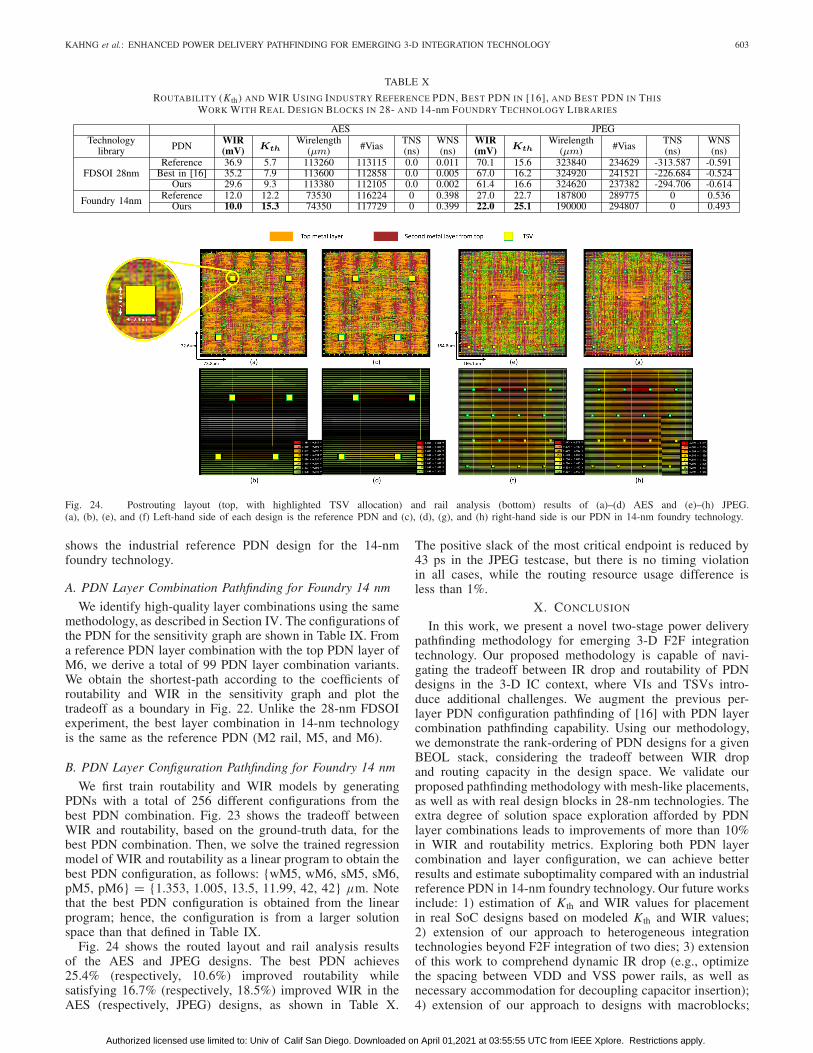
TABLE X
ROUTABILITY (Kth) AND WIR USING INDUSTRY REFERENCE PDN, BEST PDN IN [16], AND BEST PDN IN THISWORK WITH REAL DESIGN BLOCKS IN 28- AND 14-nm FOUNDRY TECHNOLOGY LIBRARIES
Fig. 24. Postrouting layout (top, with highlighted TSV allocation) and rail analysis (bottom) results of (a)–(d) AES and (e)–(h) JPEG.(a), (b), (e), and (f) Left-hand side of each design is the reference PDN and (c), (d), (g), and (h) right-hand side is our PDN in 14-nm foundry technology.
shows the industrial reference PDN design for the 14-nmfoundry technology.
A. PDN Layer Combination Pathfinding for Foundry 14 nm
We identify high-quality layer combinations using the samemethodology, as described in Section IV. The configurations ofthe PDN for the sensitivity graph are shown in Table IX. Froma reference PDN layer combination with the top PDN layer ofM6, we derive a total of 99 PDN layer combination variants.We obtain the shortest-path according to the coefficients ofroutability and WIR in the sensitivity graph and plot thetradeoff as a boundary in Fig. 22. Unlike the 28-nm FDSOIexperiment, the best layer combination in 14-nm technologyis the same as the reference PDN (M2 rail, M5, and M6).
B. PDN Layer Configuration Pathfinding for Foundry 14 nm
We first train routability and WIR models by generatingPDNs with a total of 256 different configurations from thebest PDN combination. Fig. 23 shows the tradeoff betweenWIR and routability, based on the ground-truth data, for thebest PDN combination. Then, we solve the trained regressionmodel of WIR and routability as a linear program to obtain thebest PDN configuration, as follows: {wM5, wM6, sM5, sM6,pM5, pM6} = {1.353, 1.005, 13.5, 11.99, 42, 42} μm. Notethat the best PDN configuration is obtained from the linearprogram; hence, the configuration is from a larger solutionspace than that defined in Table IX.
Fig. 24 shows the routed layout and rail analysis resultsof the AES and JPEG designs. The best PDN achieves25.4% (respectively, 10.6%) improved routability whilesatisfying 16.7% (respectively, 18.5%) improved WIR in theAES (respectively, JPEG) designs, as shown in Table X.
The positive slack of the most critical endpoint is reduced by43 ps in the JPEG testcase, but there is no timing violationin all cases, while the routing resource usage difference isless than 1%.
X. CONCLUSION
In this work, we present a novel two-stage power deliverypathfinding methodology for emerging 3-D F2F integrationtechnology. Our proposed methodology is capable of navi-gating the tradeoff between IR drop and routability of PDNdesigns in the 3-D IC context, where VIs and TSVs intro-duce additional challenges. We augment the previous per-layer PDN configuration pathfinding of [16] with PDN layercombination pathfinding capability. Using our methodology,we demonstrate the rank-ordering of PDN designs for a givenBEOL stack, considering the tradeoff between WIR dropand routing capacity in the design space. We validate ourproposed pathfinding methodology with mesh-like placements,as well as with real design blocks in 28-nm technologies. Theextra degree of solution space exploration afforded by PDNlayer combinations leads to improvements of more than 10%in WIR and routability metrics. Exploring both PDN layercombination and layer configuration, we can achieve betterresults and estimate suboptimality compared with an industrialreference PDN in 14-nm foundry technology. Our future worksinclude: 1) estimation of Kth and WIR values for placementin real SoC designs based on modeled Kth and WIR values;2) extension of our approach to heterogeneous integrationtechnologies beyond F2F integration of two dies; 3) extensionof this work to comprehend dynamic IR drop (e.g., optimizethe spacing between VDD and VSS power rails, as well asnecessary accommodation for decoupling capacitor insertion);4) extension of our approach to designs with macroblocks;
Authorized licensed use limited to: Univ of Calif San Diego. Downloaded on April 01,2021 at 03:55:55 UTC from IEEE Xplore. Restrictions apply.

604 IEEE TRANSACTIONS ON VERY LARGE SCALE INTEGRATION (VLSI) SYSTEMS, VOL. 29, NO. 4, APRIL 2021
and 5) extension of this work to foundry sub-7-nm technologynodes where BEOL resistance (along with scaling boosters,such as supervias or buried power rails) will significantlyexpand the PDN-IR pathfinding solution space.
ACKNOWLEDGMENT
The authors would like to thank Dr. Kambiz Samadi for hiscontribution in the work in [16].
REFERENCES
[1] K. Arabi, K. Samadi, and Y. Du, “3D VLSI: A scalable integrationbeyond 2D,” in Proc. Symp. Int. Symp. Phys. Des., 2015, pp. 1–7.
[2] R. Bhooshan, “Novel and efficient IR-drop models for designing powerdistribution network for sub-100nm integrated circuits,” in Proc. 8th Int.Symp. Qual. Electron. Des. (ISQED), Mar. 2007, pp. 287–292.
[3] U. Brenner and A. Rohe, “An effective congestion-driven placementframework,” IEEE Trans. Comput.-Aided Design Integr. Circuits Syst.,vol. 22, no. 4, pp. 387–394, Apr. 2003.
[4] A. E. Caldwell, A. B. Kahng, S. Mantik, I. L. Markov, andA. Zelikovsky, “On wirelength estimations for row-based placement,”IEEE Trans. Comput.-Aided Design Integr. Circuits Syst., vol. 18, no. 9,pp. 1265–1278, Aug. 1999.
[5] W.-T.-J. Chan, P.-H. Ho, A. B. Kahng, and P. Saxena, “Routabilityoptimization for industrial designs at sub-14nm process nodes usingmachine learning,” in Proc. ACM Int. Symp. Phys. Des., Mar. 2017,pp. 15–21.
[6] W.-T. J. Chan, Y. Du, A. B. Kahng, S. Nath, and K. Samadi, “3D-ICbenefit estimation and implementation guidance from 2DIC implemen-tation,” in Proc. DAC, 2015, pp. 1-6.
[7] W.-H. Chang et al., “Generating routing-driven power distribution net-works with machine-learning technique,” IEEE Trans. Comput.-AidedDesign Integr. Circuits Syst., vol. 36, no. 8, pp. 1237–1250, Aug. 2017.
[8] K. Chang et al., “Cascade2D: A design-aware partitioning approach tomonolithic 3D IC with 2D commercial tools,” in Proc. ICCAD, 2016,pp. 1–8.
[9] K. Chang, S. Das, S. Sinha, B. Cline, G. Yeric, and S. K. Lim,“Frequency and time domain analysis of power delivery network formonolithic 3D ICs,” in Proc. IEEE/ACM Int. Symp. Low Power Electron.Des. (ISLPED), Jul. 2017, pp. 1–6.
[10] K. Chang, A. Koneru, K. Chakrabarty, and S. K. Lim, “Design automa-tion and testing of monolithic 3D ICs: Opportunities, challenges, andsolutions: (Invited paper),” in Proc. IEEE/ACM Int. Conf. Comput.-AidedDes. (ICCAD), Nov. 2017, pp. 805–810.
[11] C.-K. Cheng, A. B. Kahng, I. Kang, and L. Wang, “RePlAce: Advancingsolution quality and routability validation in global placement,” IEEETrans. Comput.-Aided Design Integr. Circuits Syst., vol. 38, no. 9,pp. 1717–1730, Sep. 2019.
[12] V. A. Chhabria, A. B. Kahng, M. Kim, U. Mallappa, S. S. Sapatnekar,and B. Xu, “Template-based PDN synthesis in floorplan and place-ment using classifier and CNN techniques,” in Proc. ASP-DAC, 2020,pp. 44–49.
[13] Y. Du, K. Samadi, and K. Arabi, “Emerging 3DVLSI: Opportunities andchallenges,” in Proc. S3S, 2015, pp. 1–5.
[14] J. H. Friedman, “Multivariate adaptive regression splines,” Ann. Statist.,vol. 19, no. 1, pp. 1–67, 1991.
[15] A. Kahng, A. B. Kahng, H. Lee, and J. Li, “PROBE: A placement,routing, back-end-of-line measurement utility,” IEEE Trans. Comput.-Aided Design Integr. Circuits Syst., vol. 37, no. 7, pp. 1459–1472,Jul. 2018.
[16] A. B. Kahng, S. Kang, S. Kim, K. Samadi, and B. Xu, “Power deliverypathfinding for emerging die-to-wafer integration technology,” in Proc.DATE, 2019, pp. 836–841.
[17] A. B. Kahng, B. Lin, and S. Nath, “Enhanced metamodeling techniquesfor high-dimensional IC design estimation problems,” in Proc. DATE,2013, pp. 1861–1866.
[18] M.-C. Kim, J. Hu, D.-J. Lee, and I. L. Markov, “A SimPLR method forroutability-driven placement,” in Proc. IEEE/ACM Int. Conf. Computer-Aided Design (ICCAD), Nov. 2011, pp. 67–73.
[19] B. W. Ku et al., “Physical design solutions to tackle FEOL/BEOLdegradation in gate-level monolithic 3D ICs,” in Proc. Int. Symp. LowPower Electron. Des., 2016, pp. 76–81.
[20] B. W. Ku, K. Chang, and S. K. Lim, “Compact-2D: A phys-ical design methodology to build commercial-quality face-to-face-bonded 3D ICs,” in Proc. Int. Symp. Phys. Des., Mar. 2018,pp. 76–81.
[21] W.-H. Liu, W.-C. Kao, Y.-L. Li, and K.-Y. Chao, “NCTU-GR 2.0:Multithreaded collision-aware global routing with bounded-length mazerouting,” IEEE Trans. Comput.-Aided Design Integr. Circuits Syst.,vol. 32, no. 5, pp. 709–722, May 2013.
[22] S. A. Panth, K. Samadi, Y. Du, and S. K. Lim, “Designand CAD methodologies for low power gate-level monolithic3D ICs,” in Proc. Int. Symp. Low power Electron. Des., 2014,pp. 171–176.
[23] S. Panth, K. Samadi, Y. Du, and S. K. Lim, “Tier-partitioning for powerdelivery vs cooling tradeoff in 3D vlsi for mobile applications,” in Proc.DAC, 2015, p. 92.
[24] S. Panth, K. Samadi, Y. Du, and S. K. Lim, “Shrunk-2D: A physicaldesign methodology to build commercial-quality monolithic 3D ICs,”IEEE Trans. Comput.-Aided Design Integr. Circuits Syst., vol. 36, no. 10,pp. 1716–1724, Oct. 2017.
[25] K. Pearson, “Note on regression and inheritance in the case of twoparents,” in Proc. Roy. Soc. London, 1895, pp. 240–242.
[26] Y. Peng, D. Petranovic, K. Samadi, P. Kamal, Y. Du, and S. K. Lim,“Inter-die coupling extraction and physical design optimization for face-to-face 3D ICs,” IEEE Trans. NANO, vol. 17, no. 4, pp. 634–644,Jul. 2017.
[27] Z. Qi, Y. Cai, and Q. Zhou, “Accurate prediction of detailed routingcongestion using supervised data learning,” in Proc. ICCD, 2014,pp. 97–103.
[28] J. A. Roy and I. L. Markov, “Seeing the forest and the trees: Steinerwirelength optimization in placement,” IEEE Trans. Comput.-AidedDesign Integr. Circuits Syst., vol. 26, no. 4, pp. 632–644, Apr. 2007.
[29] S. K. Samal, K. Samadi, P. Kamal, Y. Du, and S. K. Lim, “Full chipimpact study of power delivery network designs in gate-level monolithic3-D ICs,” IEEE Trans. Comput.-Aided Design Integr. Circuits Syst.,vol. 36, no. 6, pp. 992–1003, Jun. 2017.
[30] C. Spearman, “The proof and measurement of association between twothings,” Amer. J. Psychol., vol. 15, no. 1, pp. 72–101, 1904.
[31] Y. Xu, Y. Zhang, and C. Chu, “FastRoute 4.0: Global router withefficient via minimization,” in Proc. Asia South Pacific Des. Autom.Conf., Jan. 2009, pp. 576–581.
[32] X. Yang, R. Kastner, and M. Sarrafzadeh, “Congestion estimationduring top-down placement,” IEEE Trans. Comput.-Aided Design Integr.Circuits Syst., vol. 21, no. 1, pp. 72–80, 2002.
[33] Q. Zhou, X. Wang, Z. Qi, Z. Chen, Q. Zhou, and Y. Cai, “An accuratedetailed routing routability prediction model in placement,” in Proc.ASQED, 2015, pp. 119–122.
[34] H. Reiter. TSMC Details Family of Chip Stacks. Accessed:Nov. 4, 2019. [Online]. Available: https://www.eetimes.com/author.asp?section_id=36&doc_id=1322075
[35] J. Rudy, Py-Earth. Accessed: Nov. 4, 2019. [Online]. Available:https://github.com/scikit-learn-contrib/py-earth
[36] G. Yeric. Three Dimensions in 3DIC—Part I. Accessed: Nov. 4, 2019.[Online]. Available: https://community.arm.com/arm-research/b/articles/posts/three-dimensions-in-3dic-part-1
[37] G. Yeric. Three Dimensions in 3DIC—Part II. Accessed: Nov. 4, 2019.[Online]. Available: https://community.arm.com/arm-research/b/articles/posts/three-dimensions-in-3dic-part-ii
[38] OpenCores: Open Source IP-Cores. Accessed: Nov. 4, 2019. [Online].Available: http://www.opencores.org
[39] Cadence Innovus User Guide. Accessed: Nov. 4, 2019. [Online]. Avail-able: https://www.cadence.com
[40] Cadence Quantus QRC Extraction Users Manual.Accessed: Nov. 4, 2019. [Online]. Available: https://www.cadence.com
[41] Cadence Voltus IC Power Integrity Solution User Guide.Accessed: Nov. 4, 2019. [Online]. Available: https://www.cadence.com
[42] ANSYS RedHawk User Guide. Accessed: Nov. 4, 2019. [Online]. Avail-able: https://www.ansys.com
[43] Synopsys Design Compiler User Guide. Accessed: Nov. 4, 2019.[Online]. Available: http://www.synopsys.com
Authorized licensed use limited to: Univ of Calif San Diego. Downloaded on April 01,2021 at 03:55:55 UTC from IEEE Xplore. Restrictions apply.