enhancement of photon absorption on thin-film semiconductor
TRANSCRIPT

Research ArticleEnhancement of Photon Absorption on Ba
𝑥Sr1−𝑥
TiO3
Thin-FilmSemiconductor Using Photonic Crystal
Abd. Wahidin Nuayi,1,2 Husin Alatas,1 Irzaman S. Husein,1 and Mamat Rahmat1
1 Department of Physics, Bogor Agricultural University, Jl. Meranti, Kampus IPB Darmaga, Bogor 16680, Indonesia2Department of Physics, University of Gorontalo, Jl. Jend. Sudirman No. 6 Kota Gorontalo, Gorontalo 96128, Indonesia
Correspondence should be addressed to Husin Alatas; [email protected]
Received 17 July 2013; Accepted 3 November 2013; Published 9 January 2014
Academic Editor: Augusto Belendez
Copyright © 2014 Abd. Wahidin Nuayi et al. This is an open access article distributed under the Creative Commons AttributionLicense, which permits unrestricted use, distribution, and reproduction in any medium, provided the original work is properlycited.
Enhancement of photon absorption on barium strontium titanate (Ba𝑥Sr1−𝑥
TiO3) thin-film semiconductor for mole fraction 𝑥 =
0.25, 0.35, 0.45, and 0.55 using one-dimensional photonic crystal with defect was investigated experimentally. The thin film wasgrown on transparent conductive oxide (TCO) substrate using chemical solution deposition method and annealed at 500∘C for 15hours with increasing rate of 1.6∘C/min. From optical characterization in visible spectrum it was found that the average absorptionpercentages are 92.04%, 83.55%, 91.16%, and 80.12%, respectively. The BST thin film with embedded photonic crystal exhibited arelatively significant enhancement on photon absorption, with increasing value of 3.96%, 7.07%, 3.04%, and 13.33% for the respectivemole fraction and demonstrating absorbance characteristic with flat feature. In addition, we also discuss the thin-film propertiesof attenuation constant and electrical conductivity.
1. Introduction
In solar cell technology, there are some materials that can beused as its base material. Three of them are CulnSe
2(or its
alloys such as CulnS2or CulnGaSe
2), CdTe, and amorphous
silicon materials. These materials only require one micronthickness to establish an efficient solar cells, due to their highlight absorption [1–4]. However, CdTe and CulnSe
2have a
bad impact on environment; namely, when the CdTe solarcells are on fire, this cadmiumwould cause harmful pollution.In laboratory scale, the CuInSe
2material has efficiency above
15%, but it is difficult to control its elements, especially whenbeing produced in larger scale, which implies that it is difficultto produce the associated module even in a laboratory scale[1, 2]. In the mean time, for amorphous silicon material, therelated solar cell has been produced in laboratory scale withefficency about 9.5% to 13% [2, 4–7].
There are several other important ferroelectric materialswhich were studied by many researchers such as PbTiO
3,
Pb (ZrxTi1−x)O3, SrBiTaO3, Pb(Mg1/3
Nb2/3
)O3, and BaTiO
3
which is the basic of (Ba,Sr)TiO3[8]. Due to its properties,
BaSrTiO3(or BST for short) is a material which has been
intensively studied and developed. One of them is in theform of BST thin-film ferroelectric which is used and utilizedin electronics such as for light sensor application that canbe developed to make solar cells according to optical andelectrical characteristics [9, 10].
BST thin film is a material with high dielectric constant,high degree of crystallinity (∼800∘C), low leakage current,and resistance to high breakdown voltage at Curie’s tem-perature, as well as high capacitance [11, 12]. This thin filmcan be produced with various methods such as metalorganicchemical vapor deposition (MOCVD) [13], sol-gel [14–17],atomic laser deposition (ALD) [18], hydrothermal synthesis[19], metal organic decomposition (MOD) [20, 21], andchemical solution deposition (CSD) [22–26].
To examine the ability of BST as a material that can beutilized as solar cell, some measurements such as its abilityin absorbing photons are required, because antireflectivematerial is more preferred in solar cell system. Photonabsorptionwill affect the efficiency of the associated solar cell.Based on this fact, we have attempted to increase the photon
Hindawi Publishing CorporationInternational Journal of OpticsVolume 2014, Article ID 534145, 8 pageshttp://dx.doi.org/10.1155/2014/534145

2 International Journal of Optics
absorption of a BST thin film grown on transparent conduc-tive oxide (TCO) glass using chemical solution deposition(CSD) method with annealing temperature of 500∘C for 15hours. To do this, we used one-dimensional photonic crystal(PhC) to trap the corresponding photon. It is well known thata PhC structure can manipulate light flow [27] due to theexistence of the so-called photonic band gap (PBG) whichprevent light to propagate in specific direction. Interestingly,when a defect layer is introduced into the PhC it will leadto the occurrence of the so-called photonic pass band (PPB)that allows a narrow window of light transmission in thecorresponding PBG [28].
The CSD method was employed in this research due toits advantages, such as relatively low processing temperature,homogeneity composition, precise control of composition,and large area deposition [15, 24]. In addition, it also offersother advantages such as stoichiometry control, homogene-ity, and low sintering temperature, and the most important isrelatively low cost.These advantages are suitable for scientificresearch and development.
As the substrate layer we considered a one-dimensionalPhC with a defect that consists of two different dielectricmaterials in a unit cell and a single defect layer in one of theunit cell. This treatment is expected to improve the sunlightabsorbance. It was shown that the utilization of PhC onsilicon solar cells can enhance photon absorption rangingfrom 15% to 26% depending on the associated PhC structures[29–32].
In this research, the combination of BST thin film withvarying mole fraction and one-dimensional PhC is studied.It is found that a remarkable enhancement can be achieved.This report aims to discuss the results.
2. Experimental Methods
Instruments used in this research are analytical balanceSartonius model SL6100, ultrasonic Branson model 2210,spin coater reactor, LCR meter (HIOKI 3522-50 LCRHitester), and VIS-NIR spectrophotometer ocean optics.Thematerials are barium acetate [Ba(CH
3COO)
2, 99%], stron-
tium acetate [Sr(CH3COO)
2, 99%], titanium isopropox-
ide [Ti(C12O4H28), 99.999%], gallium trioxide [Ga
2O3], 2-
methoxyethanol [H3COOCH
2CH2OH, 99%], ethanol 96%,
TCO glass, distilled water, silver paste, preparate glass, andaluminum foil. All these materials are from Sigma Aldrich.
As the first step in BST thin-film manufacturing, weprepared substrate of transparent conductive oxide (TCO);after that BST solution is made by reacting barium acetate,strontium acetate, titanium isopropoxide, and 5mL of 2-methoxyethanol solvent using Branson Model 2210 ultra-sonic for 90 minutes. Besides BST solution, BGST solutionis made in the same way as BST solution, plus adding galliumoxide at 10% of the mass of BST. BGST and BST solutions areused as p-type andn-type layers, respectively.Next step is filmgrowth processing; in this step, p-type layer manufacturing isdone first then n-type layer. P-type layer (BGST solution) isgrown by using spin coating reactor with speed of 6000 rpmfor 30 seconds. For the n-type growth, its process is similar as
p-type growth, but it is done after the p-type layer has beenannealed.
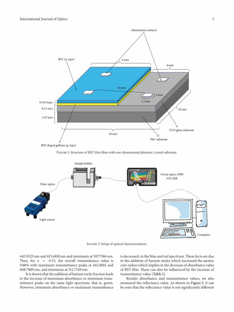
The two last steps are annealing process and contactinstallation using aluminium metallization process. Anneal-ing process, which aims to diffuse BST solution to substrate,is conducted at temperature of 500∘C with increasing rate of1.67∘C/minutes and held up for 15 hours. The BST thin-filmstructure with photonic crystals layer is shown in Figure 1.
The optical characterizations of BST thin film, whichare performed by using VIS-NIR optical spectroscopy oceanoptics DT-mini-2 model, include measurements and cal-culations of absorbance, transmittance, absorbance coeffi-cient, and attenuation coefficient. The setup processing ofoptical characterization is shown in Figure 2. While theelectrical characterizations, that is, electrical conductivity,was carried out by measuring electrical conductance usingLCR meter HIOKI 3522-50 LCR HiTester type, conductancemeasurements of these thin films were done at frequencyof 100 kHz. The setup processing of electrical conductancecharacterization is shown in Figure 3.
3. Results and Discussions
3.1. Absorbance and Transmittance. The optical characteri-zations of BST thin film are performed in the wavelengthof 400–800 nm. Absorbance (𝐴), transmittance (𝑇), andreflectance (𝑅) values are expressed in percentage. Theabsorbance percentage is obtained based on the relationshipthat the total amount of absorbance, transmittance, andreflectance is equal to one (𝐴 + 𝑇 + 𝑅 = 1).
Figure 4(a) shows that the overall absorbance percentageof BST thin film has light absorption almost in every visiblelight spectrum range, even in the infrared region withabsorption value more than 67.6%. In addition, it is indicatedthat themaximum absorbance of BST thin film for all bariummole fractions is in the range of 457 nm ≤ 𝜆 ≤ 570 nm,and the minimum absorbance spectrum is in 570 nm ≤ 𝜆 ≤678 nm. The largest absorbance was found at mole fraction𝑥 = 0.25 with average absorbance value of 92.04% andmaximum and minimum absorbance peaks at wavelength of502.7623 nm and 657.7201 nm, respectively. For 𝑥 = 0.35,average absorbance value decreased to 83.55% with maxi-mum and minimum peaks at wavelength of 506.4238 nmand 613.6818 nm, respectively. Then, absorbance value isincreased to 91.16% at𝑥 = 0.45withmaximumandminimumabsorbance peaks at 507.7586 nm and 618.5747 nm, respec-tively. For 𝑥 = 0.55, overall average absorbance decreasedto 80.12% with maximum and minimum absorbance peaksat 512.7549 nm and 608.7889 nm, respectively. Minimumabsorbance value implies that electron did not absorb thephoton energy.This means that most of them are transmittedor reflected.
Figure 4(b) shows that maximum absorbance value hasthe lowest transmittance value at 𝑥 = 0.25 with overallaverage transmittance value of 3.79% with maximum trans-mittance peaks at 462.7919 and 657.7201 nm and minimumat 502.7623 nm. For 𝑥 = 0.35, the overall average transmit-tance value is 8.25% with maximum transmittance peaks at
International Journal of Optics 3
Aluminium contacts
PhC substrate
BST (n-type)
BST doped gallium (p-type)
TCO glass substrate
6mm
0.5674𝜇m
10mm
10mm
10mm
1.5mm
2mm
4mm
0.51mm
1.07mm
Figure 1: Structure of BST thin films with one-dimensional photonic crystal substrate.
Light source
Sample holder
Computer
Ocean optics 2000VIS-NIR
Fiber optics
Figure 2: Setup of optical characterization.
445.9323 nm and 613.6818 nm and minimum at 507.7586 nm.Then, for 𝑥 = 0.55, the overall transmittance value is9.88% with maximum transmittance peaks at 442.8061 and608.7889 nm, and minimum at 512.7549 nm.
It is shown that the addition of bariummole fraction leadsto the increase of maximum absorbance or minimum trans-mittance peaks on the same light spectrum, that is, green.However, minimum absorbance or maximum transmittance
is decreased, in the blue and red spectrum.These facts are dueto the addition of barium moles which increased the atomiccore radius which implies in the decrease of absorbance valueof BST film. These can also be influenced by the increase oftransmittance value (Table 1).
Besides absorbance and transmittance values, we alsomeasured the reflectance value. As shown in Figure 5, it canbe seen that the reflectance value is not significantly different

4 International Journal of Optics
Contact 1 Contact 3
Contact 2 Contact 4
LCR meter
Cable
t 1 Contac
Figure 3: Setup of electrical conductance characterization.
Wavelength (nm)400 500 600 700 800
Abso
rban
ce (%
)
065
70
75
80
85
90
95
100
(a)
Wavelength (nm)400 500 600 700 800
Tran
smitt
ance
(%)
0
2
4
6
8
10
12
14
16
18
(b)
Figure 4: Relation between wavelength and (a) absorbance; (b) transmittance of BST thin films for mole fractions 𝑥 = 0.25 (—Δ—), 𝑥 =0.35 (—◻—), 𝑥 = 0.45 (—I—), and 𝑥 = 0.55 (—◊—).
from the transmittance and shares similar maximum andminimum reflectance peak patterns but with different values.This is consistent with the theory that when a material hasthe maximum absorbance value, so the transmittance andreflectance are minimum. Based on the average absorbancevalue more than 80.12% or the average transmittance andreflectance values less than 10% indicates that BST materialwhich is employed in this study can be utilized as amaterial inthe solar cell manufacturing, because one of the requirementsof solar cell material is antireflective material [1, 7].
The PhC with defect that is used in this study as theBST thin-film substrate consists of 11 unit cells with eachcomposed of two different dielectricmaterials of high and lowrefractive indices, namely, OS-5 (alloy of ZrO
2and TiO
2) and
MgF2with refractive indices of 2.1 and 1.38, respectively, and
it was fabricated using electron beam evaporation methodon substrate of standard glass material borosilicate crown
(known as BK-7) with a refractive index of 1.52. Details ofthis fabricated PhC can be found in [33]. We inserted a singledefect layer with different thickness in the related PhC suchthat a PPB occurred inside the associated PBG. Based onthe results of UV-VIS spectroscopic measurements, as shownin Figure 6, the range of 400–612 nm corresponds to PBGof PhC, with the localized PPB transmittance being around510.5300 nm.
When a polychromatic light is exposed to BST thin filmwith the embedded PhC, a part of light with specific wave-length is absorbed and transmitted by BST layer. However,there is a part of polychromatic lightwhich is directly exposedto the PhC, especially on substrate surface which is not coatedby BST. The light which is directly exposed to the surface ofPhC and light with specific wavelength which is transmittedby BST layer are reflected back by PhC to BST.The total lightspectrawhich are reflected by the PhC layer are then absorbed
International Journal of Optics 5
Table 1: The shift of maximum and minimum absorbance andtransmittance wavelengths of BST film caused by addition ofbarriums mole fraction.
Mole fraction (𝑥) Wavelength, 𝜆 (nm)Absorbance Transmittance
0.25 502.7623a 462.7919a dan 657.7201a
657.7201b 502.7623b
0.35 506.4238a 445.9323a dan 613.6818a
613.6818b 506.4238b
0.45 507.7586a 452.7993a dan 618.5747a
618.5747b 507.7586b
0.55 512.7549a 442.8061a dan 608.7889a
608.7889b 512.7549baMaximum absorption peak; bminimum absorption peak.
Wavelength (nm)400 500 600 700 800
Refle
ctan
ce (%
)
02468
1012141618
Figure 5: Relation betweenwavelength and reflectance value of BSTthin films for mole fractions, 𝑥 = 0.25 (—Δ—), 𝑥 = 0.35 (—◻—),𝑥 = 0.45 (—I—), and 𝑥 = 0.55 (—◊—).
again by BST layer, so the absorbed light by BST is expectedto be increased.
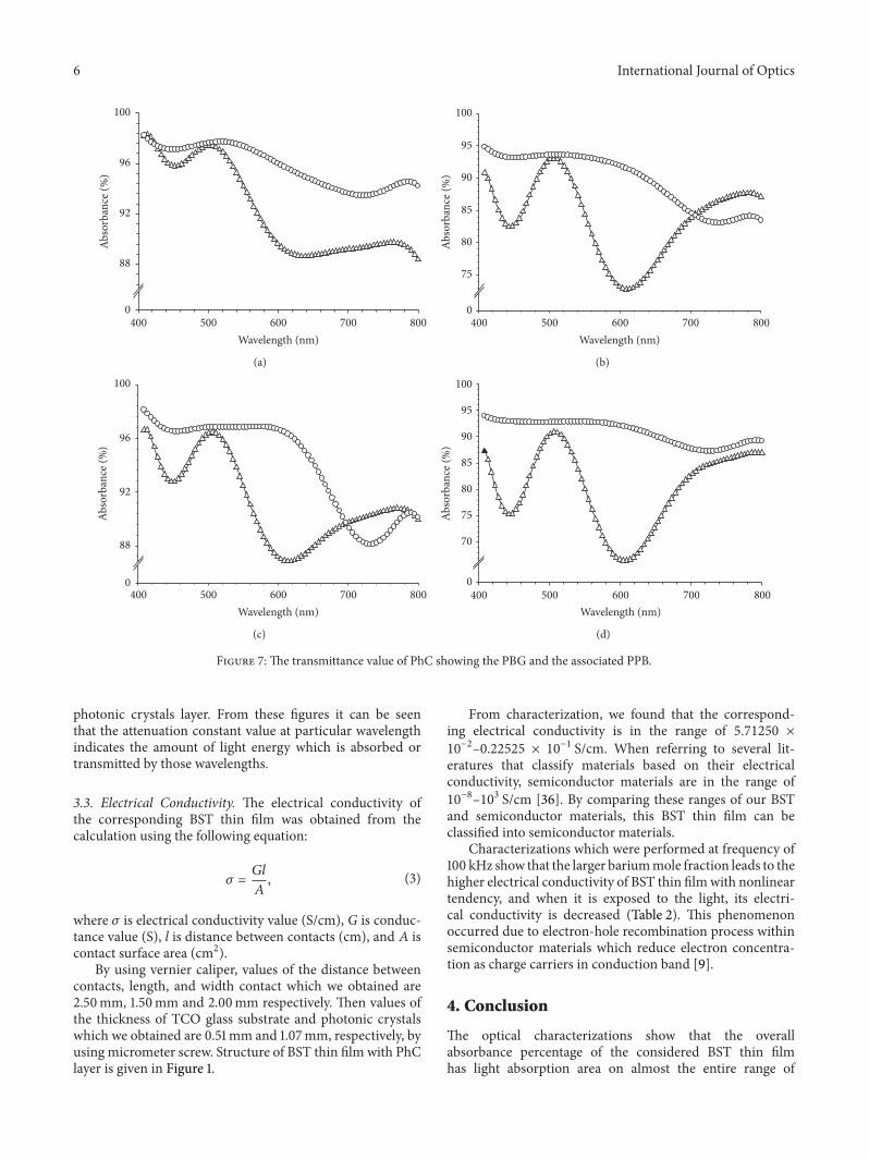
Significant changes in absorbance occurred when thePhC is applied to the associated BST thin-film. As shownin Figure 7, our BST thin film with embedded PhC showsincreasing absorption for all 𝑥 values in the range of 3.04% to13.33%. For 𝑥 = 0.25, the overall average absorbance percent-age increased by 3.96% from 92.4% into 95.68% (Figure 7(a)).For 𝑥 = 0.35, the average absorbance percentage increased by7.07% into 89.45% from 83.55% (Figure 7(b)). Furthermore,the overall average absorbance at 𝑥 = 0.45 increases fromthe 91.16% to 93.93% or increased only by 3.04% which is thelowest (Figure 7(c)), and 𝑥 = 0.55 has the highest averageabsorbance percentage, that is, by 13.33% from 80.13% into90.81%. (Figure 7(d)).
The largest absorbance was found at the mole fraction x= 0.55 with the highest being in orange spectrum (37.71%),followed by yellow spectrum which is 33.53%. Next, thereare purple, red, blue, and green spectra with the amountof 17.85%, 12.32%, 11.24%, and 9.96%, respectively, while thelowest absorbance occurred at 𝑥 = 0.25 except red spectrum(for 𝑥 = 0.45). The lowest absorbance percentage is in purple
Wavelength (nm)400 500 600 700 800
Tran
smitt
ance
(%)
0
20
40
60
80
100
Figure 6: Comparison between absorbance of BST thin films with(—I—) and without (—Δ—) photonic crystals for mole fraction (a)𝑥 = 0.25, (b) 𝑥 = 0.35 (c) 𝑥 = 0.45, and (d) 𝑥 = 0.55.
spectrum with an increase of only 0.39% followed by blue,green, red, yellow, and orange spectra with the amount of0.87%, 2.08%, 2.55%, 6.44%, and 7.03%, respectively.
Higher absorbance of BST thin films, which is expressedin a percentage and varies for each 𝑥 mole fraction, whencompared to thin films without photonic crystals layer, is dueto structure and characterization of photonic crystals layer.Remarkably, an almost flat absorbance feature in range of400 to 700 nm was exhibited as shown in Figure 7, especiallyfor 𝑥 = 0.45. This interesting feature can be explainedas the result of mutual combination between BST thin-filmabsorbance characteristic and transmittance of PhC given inFigure 6.
3.2. Attenuation Constant (k). It is well known that whenlight with specific wavelength illuminates a material, thecorresponding intensity will be attenuated on short distance.In this condition, the wave’s amplitude will decrease expo-nentially, with different intensity reduction for each material[34]. One of the parameters which is used to determine theattenuation effect is from its attenuation constant (𝑘). Byusing (1), the value of 𝑘 in this study can be determined fromthe following relation [35]:
𝛼 =
4𝜋𝑘
𝜆
, (1)
where 𝑘 is attenuation constant value, 𝜆 is wavelength (m),and𝛼 is absorbance coefficient (cm−1) which is obtained fromthe transmittance data using the following equation:
𝛼 =
ln (1/𝑇)𝑑
, (2)
where 𝑇 is amount of transmittance and 𝑑 is the thickness ofBST films layer; in this study 𝑑 = 0.576 𝜇m,which is obtainedby using volumetric method.
Figures 8(a) and 8(b) show attenuation constant as awavelength function of BST thin films with and without
6 International Journal of Optics
Wavelength (nm)400 500 600 700 800
Abso
rban
ce (%
)
0
88
92
100
96
(a)
Abso
rban
ce (%
)
Wavelength (nm)400 500 600 700 800
0
75
80
85
90
95
100
(b)
Wavelength (nm)400 500 600 700 800
0
88
92
96
100
Abso
rban
ce (%
)
(c)
Wavelength (nm)400 500 600 700 800
0
70
75
80
85
90
95
100
Abso
rban
ce (%
)
(d)
Figure 7: The transmittance value of PhC showing the PBG and the associated PPB.
photonic crystals layer. From these figures it can be seenthat the attenuation constant value at particular wavelengthindicates the amount of light energy which is absorbed ortransmitted by those wavelengths.
3.3. Electrical Conductivity. The electrical conductivity ofthe corresponding BST thin film was obtained from thecalculation using the following equation:
𝜎 =
𝐺𝑙
𝐴
, (3)
where 𝜎 is electrical conductivity value (S/cm), G is conduc-tance value (S), l is distance between contacts (cm), and 𝐴 iscontact surface area (cm2).
By using vernier caliper, values of the distance betweencontacts, length, and width contact which we obtained are2.50mm, 1.50mm and 2.00mm respectively. Then values ofthe thickness of TCO glass substrate and photonic crystalswhich we obtained are 0.51mm and 1.07mm, respectively, byusing micrometer screw. Structure of BST thin film with PhClayer is given in Figure 1.
From characterization, we found that the correspond-ing electrical conductivity is in the range of 5.71250 ×10⁻²–0.22525 × 10⁻¹ S/cm. When referring to several lit-
eratures that classify materials based on their electricalconductivity, semiconductor materials are in the range of10−8–103 S/cm [36]. By comparing these ranges of our BST
and semiconductor materials, this BST thin film can beclassified into semiconductor materials.
Characterizations which were performed at frequency of100 kHz show that the larger bariummole fraction leads to thehigher electrical conductivity of BST thin filmwith nonlineartendency, and when it is exposed to the light, its electri-cal conductivity is decreased (Table 2). This phenomenonoccurred due to electron-hole recombination process withinsemiconductor materials which reduce electron concentra-tion as charge carriers in conduction band [9].
4. Conclusion
The optical characterizations show that the overallabsorbance percentage of the considered BST thin filmhas light absorption area on almost the entire range of

International Journal of Optics 7
Wavelength (nm)400 500 600 700 800
010
15
20
25
30
35k
(×10−2)
(a)
Wavelength (nm)400 500 600 700 800
0
10
20
30
40
k(×10−2)
(b)
Figure 8: Relation betweenwavelength and attenuation constant of BST thin filmswithout (a) andwith (b) photonic crystals formole fraction𝑥 = 0.25 (—Δ—), 𝑥 = 0.35 (—◻—), 𝑥 = 0.45 (—I—) and 𝑥 = 0.55 (—◊—).
Table 2: Electrical conductivity value (𝜎) of BST thin films after exposed by light with intensity more than 2000 lux (bright condition).
Mole fraction (𝑥)𝜎 (×10−1 S/cm) Reduction percentage 𝜎 (%)
Dark BrightA B A B A B
0.25 0.57125 0.22525 0.24813 0.20508 130,22206 9,835190.35 5.10250 0.51025 3.25333 0.43117 56,83930 18,340790.45 4.96366 1.05475 1.21908 1.03142 307,16442 2,261930.55 3.50833 1.86517 2.10444 1.08008 66,71086 72,68813Conducted relatively to mole fraction 𝑥 = 0.25; A: without photonic crystals layer; B: with photonic crystals layer.
the visible light spectrum even to the infrared range withabsorption value more than 67.6%. For 𝑥 = 0.25, 0.35, 0.45,and 0.55 visible spectra have average absorption percentagesof 92.04%, 83.55%, 91.16%, and 80.12%, respectively.
A significant change occurred when PhC substrate isembedded in BST thin film which shows increasing inphotons absorption in the wavelength of 400–780 nm; thoseare 3.96%, 7.07%, 3.04%, and 13.33% for 𝑥 = 0.25, 0.35,0.45, and 0.55, respectively. A remarkable feature of almostflat absorbance characteristics was observed. This featureoccurred due to mutual combination between BST thin filmand the corresponding PhC with defect.
By considering solar cell material ability in absorbingphotons, it can be concluded that the associated BSTmaterialcan be further utilized as a solar cell material; however,further testing on other solar cell properties is required suchas photovoltaic characteristics, fill factor, and efficiency scalein photon-to-current conversion process.
Conflict of Interests
The authors declare that there is no conflict of interestsregarding the publication of the paper.
Acknowledgments
This work is supported by National Innovation System(SINas) Research Grant from the Ministry of Researchand Technology, Republic of Indonesia, under contract no.38/SEK/INSINAS/PPK/I/2013. Nuayi would like to thank theMinistry of Education andCulture, Republic of Indonesia, forhis postgraduate funding through BPPS scholarship.
References
[1] R. H. Bossert, C. J. J. Tool, J. A. M. van Roosmalen, C. H.M. Wentink, and M. J. M. de Vaan, “Thin-film solar cells,technology evaluation and perspectives,” Tech. Rep., 2000,http://citeseerx.ist.psu.edu/viewdoc/download?doi=10.1.1.196.7245&rep=rep1&type=pdf.
[2] K. L. Chopra, P. D. Paulson, and V. Dutta, “Thin-film solar cells:an overview,” Progress in Photovoltaics, vol. 12, no. 2-3, pp. 69–92, 2004.
[3] Y. Guo, L. Huang, and A. L. Porter, “The research profilingmethod applied to nano-enhanced, thin-film solar cells,” R &DManagement, vol. 40, no. 2, pp. 195–208, 2010.
[4] T. V. Torchynska and G. Polupan, “High efficiency solar cell forspace applications,” Superficies y Vacıo, vol. 17, pp. 21–25, 2004.

8 International Journal of Optics
[5] R. B. Bergmann, “Crystalline Si thin-film solar cells: a review,”Applied Physics A, vol. 69, no. 2, pp. 187–194, 1999.
[6] A. G. Aberle, “Thin-film solar cells,” Thin Solid Films, vol. 517,no. 17, pp. 4706–4710, 2009.
[7] W. W. Wenas, “Teknologi sel surya: Perkembangan dewasa inidan yang akan datang,” 2004, http://www.energi.lipi.go.id/.
[8] J. W. Kim, T. Osumi, M. Mastuoka et al., “Preparation andcharacterization of Ba(Zr
𝑥Ti1−𝑥
)O3thin films using reactive
sputtering method,” Japanese Journal of Applied Physics, vol. 51,pp. 1–5, 2012.
[9] Irzaman, “Studi fotodiode film tipis semikonduktorBa0,6Sr0,4TiO3
didadah tantalum,” Jurnal Sains MaterialIndonesia, vol. 10, pp. 18–22, 2008.
[10] Irzaman, A. Arif, H. Syafutra, and M. Romzie, “Studi konduk-tivitas listrik, kurva I-V, dan celah energi fotodioda berbasis filmtipis semikonduktor Ba
0,75Sr0,25
TiO3(BST) yang didadah gal-
ium (BST) menggunakan metode chemical solution deposition(CSD),” Jurnal Aplikasi Fisika, vol. 5, pp. 22–30, 2009.
[11] A. Ioachim, M. I. Toacsan, L. Nedelcu et al., “Dielectric prop-erties of (Ba,Sr)TiO
3thin films for applications in electronics,”
Romanian Journalof Information Science and Technology, vol. 10,pp. 347–354, 2007.
[12] F. M. Pontes, E. R. Leite, D. S. L. Pontes et al., “Ferroelectric andoptical properties of Ba
0.8Sr0.2TiO3thin film,” Journal of Applied
Physics, vol. 91, no. 9, pp. 5972–5978, 2002.[13] F. Fitsilis, S. Regnery, P. Ehrhart et al., “BST thin films grown in
amultiwaferMOCVD reactor,” Journal of the EuropeanCeramicSociety, vol. 21, no. 10-11, pp. 1547–1551, 2001.
[14] S. B. Singh, H. B. Sharma, H. N. K. Sarma, and S. Phanjoubam,“Optical and structural properties of nano-sized barium stron-tium titanate (Ba
0.6Sr0.4TiO3) thin film,”Modern Physics Letters
B, vol. 22, no. 9, pp. 693–700, 2008.[15] Y. Xin, R. Wei, S. Peng, W. Xiaoqing, and Y. Xi, “Enhanced tun-
able dielectric properties of Ba0.5Sr0.5TiO3/Bi1.5Zn1.0Nb1.5O7
multilayer thin films by a sol-gel process,”Thin Solid Films, vol.520, no. 2, pp. 789–792, 2011.
[16] N. B. Ibrahim, E. Yusrianto, Z. Zalita, and Z. Ibarahim, “Effectof annealing temperature of Sol-Gel TiO
2buffer layer on
microstructure and electrical properties of Ba0.6Sr0.4TiO3films,”
Sains Malaysiana, vol. 41, no. 3, pp. 339–344, 2012.[17] K. Verma, S. Sharma, D. K. Sharma, R. Kumar, and R. Rai,
“Sol gel processing and characterization of nanometersized (Ba,Sr)TiO
3ceramics,”AdvancedMaterials Letters, vol. 3, pp. 44–49,
2012.[18] M. Tyunina, M. Plekh, J. Levoska et al., “Dielectric properties
of atomic layer deposited thin-film barium strontium titanate,”Integrated Ferroelectrics, vol. 102, no. 1, pp. 29–36, 2008.
[19] D. Gao, D. Xiao, J. Bi et al., “Hydrothermal syntheses of bariumstrontium titanate thin films,” Materials Transactions, vol. 44,no. 7, pp. 1320–1323, 2003.
[20] I. P. Koutsaroff, A. Kassam, M. Zelner et al., “Dielectric prop-erties of (Ba,Sr)TiO
3thin film capacitors fabricated on alumina
substrates,”MRS Proceedings, vol. 748, article U6.1, 2003.[21] P. M. Suherman, Y. Y. Tse, T. J. Jackson et al., “Comparison of
structural, microstructural, and electrical analyses of bariumstrontium titanate thin films,” Journal of Applied Physics, vol.105, no. 6, Article ID 061604, 2009.
[22] Y. Iriani, M. Hikam, B. Soegijono, and I. Mudzakir, “Pen-garuh heating rate dan jumlah lapisan terhadap sifat listrik(kurva histeresis) pada lapisan tipis Barium Strontium Titanat,”Indonesian Journal of Materials Science, pp. 205–208, 2008.
[23] Irzaman, A.Marwan, A. Arief, R. A. Hamdani, andM. Komaro,“Electrical conductivity and surface rougness properties offerroelectric gallium doped Ba
0.5Sr0.5TiO3(BGST) thin film,”
Indonesian Journal of Physics, vol. 19, pp. 119–121, 2008.[24] Irzaman, H. Syafutra, H. Darmasetiawan et al., “Electrical
properties of photodiodeBa0.25
Sr0.75
TiO3(BST) thin filmdoped
with ferric oxide on p-type Si (100) substrate using chemicalsolution deposition method,” Atom Indonesia, vol. 37, pp. 133–138, 2011.
[25] N. Sirikulrat, “Colossal dielectric constant and a microfaradtunable capacitance in platinum thin film-antimony dopedBarium Strontium Titanate Schottky barrier diodes,”Thin SolidFilms, vol. 520, no. 1, pp. 633–640, 2011.
[26] S. M. Aygun, J. F. Ihlefeld, W. J. Borland, and J.-P. Maria,“Permittivity scaling in Ba
1−𝑥Sr𝑥TiO3thin films and ceramics,”
Journal of Applied Physics, vol. 109, no. 3, Article ID 034108, 2011.[27] J. D. Joannopoulos, S. G. Johnson, J. N. Winn, and R. D.
Meade, Photonic Crystal: Molding the Flow of Light, PrincetonUniversity Press, Princeton, NJ, USA, 2008.
[28] H. Alatas, H. Mayditia, H. Hardhienata, A. A. Iskandar, andM. O. Tjia, “Single-frequency refractive index sensor based ona finite one-dimensional photonic crystals with two defects,”Japanese Journal of Applied Physics, vol. 45, pp. 6754–6758, 2006.
[29] P. Bermel, C. Luo, L. Zeng, L. C. Kimerling, and J. D.Joannopoulos, “Improving thin-film crystalline silicon solar cellefficiencies with photonic crystals,” Optics Express, vol. 15, no.25, pp. 16986–17000, 2007.
[30] A. Chutinan, N. P. Kherani, and S. Zukotynski, “High-efficiencyphotonic crystal solar cell architecture,” Optics Express, vol. 17,no. 11, pp. 8871–8878, 2009.
[31] Y. Park, E. Drouard, O. E. Daif et al., “Absorption enhancementusing photonic crystals for silicon thin film solar cells,” OpticsExpress, vol. 17, no. 16, pp. 14312–14321, 2009.
[32] A. Deinega and S. John, “Solar power conversion efficiencyin modulated silicon nanowire photonic crystals,” Journal ofApplied Physics, vol. 112, no. 7, Article ID 074327, 2012.
[33] W. Maulina, M. Rahmat, E. Rustami et al., “Fabrication andcharacterization of NO
2gas sensor based on one dimensional
photonic crystal for measurement of air pollution index,” inProceedings of the 2nd International Conference on Instrumen-tation, Communication, Information Technology and BiomedicalEngineering (ICICI-BME ’11), pp. 352–355, Bandung, Indonesia,November 2011.
[34] A. Maddu and G. E. Timuda, “Pengaruh ketebalan terhadapsifat optik lapisan semikonduktor Cu
2O yang dideposisikan
dengan metode chemical bath deposition (CBD),” Jurnal IlmuPengetahuan dan Teknologi Telaah, vol. 28, pp. 1–5, 2010.
[35] W. J. Leng, C. R. Yang, J. H. Zhang et al., “Structural andoptical properties of Ba
𝑥Sr1−𝑥TiO3thin films on indium tin
oxide/quartz substrates prepared by radio-frequency mag-netron sputtering,” Journal of Applied Physics, vol. 99, no. 11,Article ID 114904, pp. 1–5, 2006.
[36] K. K. Ng, Complete Guide to Semiconductor Device, McGraw-Hill, New York, NY, USA, 1995.

Submit your manuscripts athttp://www.hindawi.com
Hindawi Publishing Corporationhttp://www.hindawi.com Volume 2014
High Energy PhysicsAdvances in
The Scientific World JournalHindawi Publishing Corporation http://www.hindawi.com Volume 2014
Hindawi Publishing Corporationhttp://www.hindawi.com Volume 2014
FluidsJournal of
Atomic and Molecular Physics
Journal of
Hindawi Publishing Corporationhttp://www.hindawi.com Volume 2014
Hindawi Publishing Corporationhttp://www.hindawi.com Volume 2014
Advances in Condensed Matter Physics
OpticsInternational Journal of
Hindawi Publishing Corporationhttp://www.hindawi.com Volume 2014
Hindawi Publishing Corporationhttp://www.hindawi.com Volume 2014
AstronomyAdvances in
International Journal of
Hindawi Publishing Corporationhttp://www.hindawi.com Volume 2014
Superconductivity
Hindawi Publishing Corporationhttp://www.hindawi.com Volume 2014
Statistical MechanicsInternational Journal of
Hindawi Publishing Corporationhttp://www.hindawi.com Volume 2014
GravityJournal of
Hindawi Publishing Corporationhttp://www.hindawi.com Volume 2014
AstrophysicsJournal of
Hindawi Publishing Corporationhttp://www.hindawi.com Volume 2014
Physics Research International
Hindawi Publishing Corporationhttp://www.hindawi.com Volume 2014
Solid State PhysicsJournal of
Computational Methods in Physics
Journal of
Hindawi Publishing Corporationhttp://www.hindawi.com Volume 2014
Hindawi Publishing Corporationhttp://www.hindawi.com Volume 2014
Soft MatterJournal of
Hindawi Publishing Corporationhttp://www.hindawi.com
AerodynamicsJournal of
Volume 2014
Hindawi Publishing Corporationhttp://www.hindawi.com Volume 2014
PhotonicsJournal of
Hindawi Publishing Corporationhttp://www.hindawi.com Volume 2014
Journal of
Biophysics
Hindawi Publishing Corporationhttp://www.hindawi.com Volume 2014
ThermodynamicsJournal of