ensc 495/851 lab 1 v3.2 april 2- 2012 glenn chapmanglennc/e495/e495la1k.pdf · ensc 495/851 lab 1...
TRANSCRIPT
ENSC 495/851 Lab 1Spring 2012 Page 1 of 9
ENSC 495/851 Lab 1 V3.2 April 2- 2012 Glenn Chapman
In the ENSC 495/851 lab you will complete a 4-mask-level, double-diffusion process starting with n type <100> wafers. At the end of the term, you will measure the electrical characteristics of devices you fabricate on these wafers. The mask levels are listed below, and the detailed processing notes can be found in Appendix A: • Mask level 1: P (Boron) diffusion windows for NPN bipolar transistors (base), PN junction diodes,
drain and source of PMOS transistor, p tubs for NMOS transistors, resistors etc. • Mask level 2: N (phosphorus) diffusion windows for transistor emitter, substrate contacts, etc. • Mask level 3: Contact windows for metal to silicon electrical connection. • Mask level 4: Metal for devise contact pads and connecting lines
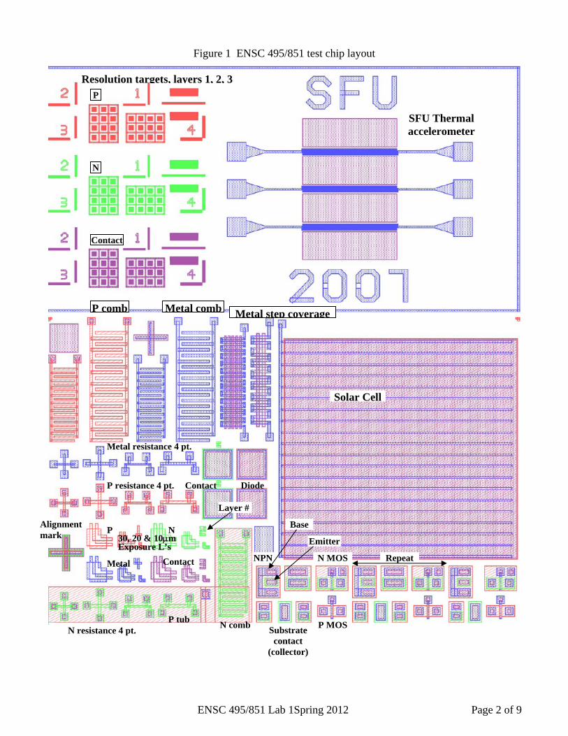
The layout of a 5mm x 6mm (W x H) ENSC 495/851 test chip is shown in Figure 1. There will be more than 200 copies of this test chip on each wafer. Below is a list of devices and test structures located on the lower part of the test chip. The smallest feature size of these devices is 20 microns. Most lines are 40 microns wide. • PN diodes • Large solar cell (big pn diode) with metal contacts • NPN bipolar transistors: 4 different designs, repeated 3 times • P MOSFET on substrate (3 copies) • N MOSFET on p tub (3 copies) • Alignment mark (+ sign for all 4 levels) • Layer number and exposure “L” test patterns (in 10, 20 and 30 microns) • CV pad (metal pads on field oxide) • Interdigitated combs of p, n+ and metal: tests for shorts between two lines separated by minimum
spacing • Metal stepping over oxide openings to watch for metal line breakage • 4 point resistance structures of p, n+ and metal • Metal contacts to substrate (with n+ below them to make better contact)
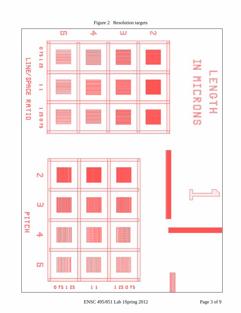
Shown in Figure 2 are 1-4 microns resolution targets for testing the photolithography/etching process capability. They contain lines and spaces from 2 to 5μm at 1.5:1, 1:1, and 1:0.75 ratios. They are located on the upper part of the test chip. An experimental SFU Thermal Accelerometer that requires a 5μm minimum feature size capability is also located in this area. (this is not used in the lab0. In Lab 1, you will go through two demo labs on oxidation and photolithography. You will carry them out and complete all the Mask level 1 boron diffusion steps and make some process related measurements. In Lab 2 you will complete 3 more mask levels of processing to complete the device fabrication, and test them at the end of the term. More notes on of your Lab 1 activities will be given in the following pages.
ENSC 495/851 Lab 1Spring 2012 Page 2 of 9
Figure 1 ENSC 495/851 test chip layout
P comb Metal comb Metal step coverage
Solar Cell
Metal resistance 4 pt.
Alignment mark
N resistance 4 pt. P tub N comb
N MOS
P MOS
NPN
Base
Emitter
Substrate contact
(collector)
Repeat
Resolution targets, layers 1, 2, 3
SFU Thermal accelerometer
P resistance 4 pt. Contact Diode
Exposure L’s
Metal
Layer #
P N
P
N
Contact
Contact
30, 20 & 10μm
ENSC 495/851 Lab 1Spring 2012 Page 3 of 9
Figure 2 Resolution targets
ENSC 495/851 Lab 1Spring 2012 Page 4 of 9
Detailed LAB 1 notes: Purpose: Grow 0.5μm oxide in steam on 4” <100> n-type silicon wafers, open boron diffusion windows with the first level mask, and carry out selective boron diffusion. These will be done in 3 student lab days, with lab demos of processes in between. Details of the each process can be found in the lab Run Sheets. Write-up: The aim of the write-up is to document what you have learned in characterizing the oxidation, definition (photolithography), and diffusion steps in Lab l. In this write-up the theory, introduction, procedure sections should be kept to a minimum. You do not put in a summary of the run sheet descriptions. However at each process you only have to document observations, results, analysis and conclusions. In particular note any deviations from the standard process, and any observations that show deviations in the results (eg differences in process times, or wafer appearance. Include captured microscope images in this report where they were taken (e.g. after etching). Final report length should be less than 15 pages, not including the lab Run Sheets and large diagrams. The write-up will be due one week after the completion of Lab 1 (tentatively Week 9 of the course). Lab 1 details and write-up instructions for each section are given below. Cross-section views of processed wafer at different stages are given in Appendix A.
Lab 1, Week 3: RCA Clean and Oxidation lab 1. RCA Clean Step (BT2_CLN—RCA Clean) Select two numbered <100> wafer, record and note those numbers. Weigh each wafer. Follow RCA Clean run sheet to clean wafers and record information on the run sheet. To minimize chemical usage and time, wafers from student groups should be cleaned at the same time. NOTE: keep good notes on anything that happened during this process that might affect the results. Draw a brief diagram of any defects you see on the wafers at any stage. RCA Cleaning Step Write-up For each step of the clean note the process step name, what you observed on the wafer (was it clean, did the step run over time, did anything go wrong). Comment on what could be done to improve the process, both from a point of speeding it up, and of increasing the cleanliness. 2. Oxidation Growth Step (BT2_WTOX--Wet Oxidation) (1) Choose a time and temperature combination to obtain that thickness of 0.5 micron in less than 1.5 hours in steam (typically this time will be given to you). Use the Oxidation Process Sheets to record your notes. Due to the time involved in this process step, all groups will put their wafers in the furnace at the same time, but each group should load the boat themselves. Note any processes deviations and exact times. (2) Inspect the wafer for defects and oxide colour. Map any defects (for each wafer). Does this colour conform to the colour charts? Make a chart of the uniformity of this colour – that is note any defects or different areas. Measure oxide thickness using the following equipment, if available:
(i) Thin-film analyzer; (ii) Weight difference before and after oxidation; (iii) Ellipsometer (if available); and (iv) Profilometer (after oxide window etched in the next lab).

ENSC 495/851 Lab 1Spring 2012 Page 5 of 9
NOTE: depending on the timing of your lab, this step may be done in the following week. Oxidation Step Writeup in Final Report (1) Note the exact time/temperature used in the process. Did anything occur that might indicate alterations in the process? (2) What did the wafers look like after growth? Was the oxide uniform. Relate the oxidation defect pattern to how the wafer was treaded in the cleaning process. (3) From the colour chart, and the time/temperature used, what is the estimated oxide thickness? Compare this to values obtained by other methods (only one wafer need be measured) listed above. Calculate the oxide thickness based on the wright method. What is the true oxide thickness as measured by the profilometer or ellipsometer? How does this compare to the expected value based on the process parameters? If there is a difference, suggest what process parameter(s) may have the largest effect on this discrepancy?
Lab 1, Week 4/5: Oxide Definition & Etch
3. Oxide Definition Step (BT3_PHTO—Photo) (Level 1 mask) (1) Define the level one mask to create the first level (diffusion mask) step. Use the Photo Process Sheets as a guide for this. Spin on the photoresist, define the pattern, develop the wafers and inspect after the development. If the definition is poor, strip photoresist and repeat this step (special process sheet available for this, BT3_RFOT—Photo Rework). Take careful note of any significant defects. (2) Etch the oxide using Buffered Oxide Etch (BOE, see BT2_OXET—Oxide Etch Process Sheet). Inspect the wafers after etching. Measure the structure sizes using the microscope and compare to those at definition. Measure the film thickness with the profilometer . Definition Step Write-up (1) In the spin coating, exposure, and development steps, did anything happen which might have affected the result? (2) After definition but before etching what type of defects did you see on the wafer? Can you suggest causes for these? (3) What was the oxide etch time? What did you use for the end point detection of this etch step, and how much over etch did you give it? On the basis of the oxide thickness determined from the growth step estimate the oxide etch rate of the BOE. (4) After oxide etching what type of defects did you see on the wafer? Can you suggest causes for these? What did you use to see if there was any remnant oxide left? (5) During the resist stripping what did you see and use to determine if the resist was removed? (6) After stripping the resist what type of defects did you see on the wafer? Can you suggest causes for these? Was any residual resist left? Did you check for edge bead and how did the edge differ from the wafers centre? (7) Measure (after photoresist stripping) the 10 micron exposure “L” test structures for oxide line and space (no oxide) widths in the x or y directions at the wafer centre, and at the wafer edge (~15-20mm from the edge). Is there any difference in “L” test structure dimension at these two different locations? Check also the resolution targets which have as fine as 1 to 4 microns lines. What resolution did you achieve? (8) Using the AlfaStep profilometer measure oxide thickness at the “L” test structures at the wafer centre, and at the wafer edge (~15-20mm from the edge). Do you notice any difference in thickness in these two locations? Compare the expected oxide thickness from the process parameters with the actual result. If there is a difference, suggest what process parameter(s) is(are) the most significant contributor of this difference.

ENSC 495/851 Lab 1Spring 2012 Page 6 of 9
Lab 1, Week 6: Boron Diffusion 4. Pre Diffusion Cleaning Step (BT2_CLN2—Modified RCA Clean) In this step you will use a modified RCA clean, with the 100:1 ratio HF solution so as not to remove the oxide. For each step of the clean note the process step name, what you observed on the wafer (was it clean, did the step run over time, did anything go wrong). Comment on what could be done to improve the process, both from a point of speeding it up, and of increasing the cleanliness. 5. Diffusion Step (BT2_BDF2—Boron Diffusion, (BT2_LTO—Low Temperature Oxidation-new) (Level 1 mask) Boron diffusion in the furnace (950ºC, 30minutes), followed by a low temperature oxidation (LTO) process (800ºC for 50 minutes). See the run sheets for details. (1) Note the exact time/temperature used in the process. Did anything occur that might indicate alterations in the process? (2) What did the wafers look like after diffusion? Relate the defect pattern to how the wafer was treated in the cleaning process. Document problems you observed (like the spots seen). (3) From the time/temperature used in this process, and from the colour chart, what oxide thickness do you expect and measure? If there is a difference suggests what process parameter(s) may have the most effect in making this difference?
Lab 1, Week 7: Boron Diffusion strip and drive in 6. Diffusion Strip and measurements Strip the LTO oxide with BOE (BT2_OXET—Oxide Etch) until dewet. Use a 4-point probe to measure the pre-deposition sheet resistance of the monitor wafer. 7. Diffusion drive in/oxidation Clean (BT2_CLN2—Modified RCA Clean) wafers and use the following parameters for the boron diffusion drive in (BT2_BDRV—Boron Drive-in and Wet Oxidation): 1150°C, 5’ dry, 60’ wet, 15’ N2. This drive-in step also grows a layer of oxide mask to be used in phosphorus diffusion in two weeks. In Week 8 (first portion of Lab 2’s first day), you will strip the oxide of the monitor wafer to measure the sheet resistance after drive in. Boron diffusions Write-up Assuming that the pre-deposition step produces a very thin layer of dopant at the solid solubility limit, what depth of layer would you estimate from the expected drive in? In this calculation assume that the initial wafer resistivity is 3 ohm cm and use this to find the background n doping level. Then find the point were the Boron dopand density equals that of the brackground levels. What doping level would you calculate from this? What sheet resistance do you expect? Compare this with value you measure and comment on any difference observed. Report the diffusion measurement results discussed above along with any comments on how the process worked.

ENSC 495/851 Lab 1Spring 2012 Page 7 of 9
Additional Lab Report Structure Lab Write-up and Process Sheets Include a combined copy of your process (run) sheets in the report. You may combined all the notes into one sheet set or create an assembled set. Attached scanned or copied version of these to the report – you will need to keep the originals for the final report. Note length of the report does not include these process sheets. Final Write-up Conclusions On the basis of the results what can you comment about where you found problems in each step – what gave you the most difficulty or created the most problem. Identify which wafer you think is the best at this point in the lab. In the report state how much work each student in your group did on the report. The Lab report will be due one week after the end of lab 1. Submit the report both in paper and electronic form (pdf file). The electronic form is so that we can collect data from all groups over the years to help us improve the fabrication process.

ENSC 495/851 Lab 1Spring 2012 Page 8 of 9
Appendix A
ENSC 495: Process description: (cross sectional sketches are schematic only; they are not to scale and do not show slopes, etc.) 1. RCA clean new, bare wafers. We will use an N type, phosphorous doped, <100>, test grade, 100 mm wafer. It is about 500
micrometers thick, is polished on one side, and has one major flat and one minor flat separated by 180 degrees. Its bulk resistivity is about 1 to 10 ohm-cm. We will perform a 4 mask process on it to form resistors, test structures, diodes, solar cells and transistors.
2. Grow a thermal field oxide (in steam) on the wafer to sufficient thickness to act as a barrier for subsequent boron doping
operation. This oxide is about 400 to 450 nanometers thick (4000 to 4500 A). It grows evenly all over the wafer.
3. Spin photoresist onto front (polished) side of wafer and soft bake. You can also protect back side of wafer with resist if
you want to keep the oxide there. This step is Photo 1 and opens vias (holes) in the oxide where we want to place boron (P type) doping.
4. Expose, develop and hard bake resist. Use a dark field mask. 5. Etch the exposed oxide in BOE (buffered oxide etch). 6. Strip resist in acetone.
Si wafer SiO2
Si SiO2
Resist
Si SiO2
Resist
Si SiO2
Resist
Si SiO2

ENSC 495/851 Lab 1Spring 2012 Page 9 of 9
7. RCA clean. 8. Using solid sources, perform boron diffusion in N2 atmosphere in furnace. Along with the boron in the silicon, some
borosilicate glass will form on the surface. This can be hard to etch, so we will perform the next step, low temperature oxidation (LTO).
9. Perform LTO (low temperature oxidation in steam) on wafer in furnace. This forms a thin, pure oxide that is more easily
etched than the boron enriched field oxide or the borosilicate glass. This should help to remove the oxide and glass in subsequent etching. Note that the LTO oxide forms under the original field oxide and borosilicate glass. It will not be as thick in the boron doped areas as in areas where it can access clean silicon.
10. Strip the wafer clean of all oxide in BOE. Patterns that were previously etched and doped will still be visible in the silicon. 11. RCA clean. 12. Perform drive-in and wet oxidation in the furnace. The boron will move slightly sideways and will be forced farther down
into the wafer. Thermal oxide is grown over the whole wafer. Note that it is slightly thinner over the boron doped areas. This oxide is our diffusion stop for phosphorous diffusion. Because it will not be stripped, it is also our insulator for subsequent steps.
13. Spin photoresist onto front (polished) side of wafer and soft bake. You can also protect back side of wafer with resist if
you want to keep the oxide there. This step is Photo 2, and opens vias in the resist where we want to place phosphorous (N type) doping. Some phosphorous will be placed in previously formed boron P wells and some in the silicon to form N++ areas for silicon substrate contact.
Si
SiO2
B
Borosilicate glass
Si B
Field SiO2
LTO SiO2 (also over B doped areas)
Si
B
Si
B
SiO2
Si SiO2 B Resist
Borosilicate glass