eprom-based 8-bit cmos microcontroller series - high tech
TRANSCRIPT

© 1994 Microchip Technology Inc. DS30015K-page 1
PIC16C5X Series
RA1RA0OSC1/CLKINOSC2/CLKOUT
RB7RB6RB5RB2
RB0RB1
RA2
DDV
RTCC
• 123456789
2019
161514131211
RA3
MCLRV
10
1817
SS
RB3 RB4
DDV VSS
PIC
16C54
MCLR
OSC1/CLKINOSC2/CLKOUT
RTCC
N/CDDV
14
2827262524232221201918171615
PIC
16C55
16C57
N/CSSV
RA0RA1RA2RA3RB0RB1RB2RB3RB4
RC7RC6RC5RC4RC3RC2RC1RC0RB7RB6RB5
1312
1011
98765432
• 1
MCLR
OSC1/CLKINOSC2/CLKOUT
RTCCSSV
14
2827262524232221201918171615
PIC
16C55
16C57
RA0RA1RA2RA3RB0RB1RB2RB3RB4
RC7RC6RC5RC4RC3RC2RC1RC0RB7RB6RB5
1312
1011
98765432
• 1
DDV
SSV
DDV
FEATURES
High-Performance RISC-like CPU• Only 33 single word instructions to learn• All single cycle instructions (200ns) except for
program branches which are two-cycle• Operating speed: DC - 20 MHz clock input
DC - 200ns instruction cycle• 12-bit wide instructions• 8-bit wide data path• 512 - 2K x 12 on-chip EPROM program memory• 25 - 72 x 8 general purpose registers (SRAM)• Seven special function hardware registers• Two-level deep hardware stack• Direct, indirect and relative addressing modes for data
and instructions
Peripheral Features• 12 - 20 I/O pins with individual direction control• 8-bit real time clock/counter (RTCC) with 8-bit
programmable prescaler• Power-On Reset
• Oscillator Start-up Timer• Watchdog Timer (WDT) with its own on-chip RC
oscillator for reliable operation• Security EPROM fuse for code-protection• Power saving SLEEP mode• EPROM fuse selectable oscillator options:
- Low-cost RC oscillator: RC- Standard crystal/resonator: XT- High-speed crystal/resonator: HS- Power saving, low frequency crystal: LP
CMOS Technology• Low-power, high-speed CMOS EPROM technology• Fully static design• Wide-operating voltage range:
- Commercial: 2.5V to 6.25V- Industrial: 2.5V to 6.25V- Automotive: 2.5V to 6.0V
• Low-power consumption- < 2mA typical @ 5V, 4 MHz- 15µA typical @ 3V, 32 KHz- < 3µA typical standby current @ 3V, 0˚C to 70˚C
FIGURE A - PIN CONFIGURATIONS
PDIP, SOIC,CERDIP Window
SSOP
PDIP, SOIC,CERDIP Window
SSOP
PIC
16C55
PIC
16C57
PIC
16C55
PIC
16C57
PIC16C5X
RA1RA0OSC1/CLKINOSC2/CLKOUT
RB7RB6RB5RB4RB3
RB0RB1RB2
RA2
SSV
RTCC
• 123456789
181716151413121110
PIC
16C54
RA3
MCLRDDV
PIC
16C54
PIC
16C56
PIC
16C54
PIC
16C56
EPROM-Based 8-Bit CMOS Microcontroller Series

PIC16C5X Series
© 1994 Microchip Technology Inc.DS30015K-page 2
Table of Contents1.0 General Description ............................................................ 31.1 Applications ......................................................................... 32.0 Architectural Description ..................................................... 32.1 Harvard Architecture ........................................................... 32.2 Clocking Scheme/Instruction Cycle ..................................... 32.3 Data Register File ............................................................... 42.4 Arithmetic/Logic Unit (ALU) ................................................. 42.5 Program Memory ................................................................ 43.0 PIC16C5X Series Overview ................................................ 53.1 UV Erasable Devices .......................................................... 53.2 One-Time-Programmable (OTP) Devices ........................... 53.3 Quick-Turnaround-Production (QTP) Devices .................... 54.0 Operational Register Files ................................................... 64.1 Indirect Data Addressing ..................................................... 64.2 Real Time Clock/Counter Register (RTCC) ........................ 64.2.1 Using RTCC with External Clock ........................................ 64.3 Program Counter ................................................................. 84.4 Stack ................................................................................... 94.5 STATUS Word Register .................................................... 114.5.1 Carry/Borrow and Digit Carry/Borrow Bits ......................... 124.5.2 Time Out and Power Down Status Bits (TO, PD) .............. 124.5.3 Program Page Preselect (PIC16C56, PIC16C57 Only) .... 124.6 f4 File Select Register (FSR) ........................................... 125.0 I/O Registers (Ports) ......................................................... 135.1 PORTA .............................................................................. 135.2 PORTB .............................................................................. 135.3 PORTC .............................................................................. 135.4 I/O Interfacing .................................................................... 135.5 I/O Programming Considerations ...................................... 145.5.1 Bidirectional I/O Ports ....................................................... 145.5.2 Successive Operations on I/O Ports ................................. 146.0 General Purpose Registers ............................................... 157.0 Special Purpose Registers ................................................ 157.1 W Working Register ....................................................... 157.2 TRISA I/O Control Register for PORTA .......................... 157.3 TRISB I/O Control Register for PORTB .......................... 157.4 TRISC I/O Control Register for PORTC .......................... 157.5 OPTION Prescaler/RTCC Option Register ....................... 158.0 Reset Condition ................................................................. 169.0 Prescaler ........................................................................... 169.1 Switching Prescaler Assignment ....................................... 1610.0 Basic Instruction Set Summary ......................................... 1710.1 Instruction Description ....................................................... 1911.0 Watchdog Timer (WDT) .................................................... 2311.1 WDT Period ....................................................................... 2311.2 WDT Programming Considerations .................................. 2312.0 Oscillator Circuits .............................................................. 2312.1 Oscillator Types ................................................................ 2312.2 Crystal Oscillator ............................................................... 2312.3 RC Oscillator ..................................................................... 2313.0 Oscillator Start-up Timer (OST) ........................................ 2513.1 Power-On Reset (POR) .................................................... 2514.0 Power Down Mode (SLEEP) ............................................. 2714.1 Wake-Up ........................................................................... 2715.0 Configuration Fuses .......................................................... 2715.1 Customer ID Code ............................................................ 2715.2 Code Protection ................................................................ 2815.2.1 Verifying a Code-Protected Part ....................................... 2816.0 Electrical Characteristics ................................................... 2916.1 Absolute Maximum Ratings .............................................. 2916.3 DC Characteristics: PIC16C5X-RC, XT, HS, LP (Com) ... 3016.4 DC Characteristics: PIC16C5XI-RC, XT, HS, LP (Ind) ..... 3116.5 DC Characteristics: PIC16C5XE-RC, XT, HS, LP (Auto) . 3216.6 DC Characteristics: PIC16C5X-RC, XT, HS, LP (Com)
and PIC16C5XI-RC, XT, HS, LP (Ind) ............................... 3316.7 DC Characteristics: PIC16C5X-RC, XT, HS, LP (Auto) ... 3416.8 AC Characteristics: PIC16C5X-RC, XT, HS, LP (Com)
and PIC16C5XI-RC, XT, HS, LP (Ind) and (Auto) ............. 3516.9 Electrical Structure of Pins ................................................ 3617.0 Timing Diagrams ............................................................... 3618.0 DC & AC Charcteristics Graphs/Tables ............................ 3719.0 Packaging Information ...................................................... 4519.1 18-Lead Plastic Dual In-Line (300 mil) .............................. 4519.2 28-Lead Dual In-Line Plastic (600 mil) .............................. 4619.3 28-Lead Dual In-Line Plastic (300 mil) .............................. 4719.4 18-Lead Plastic Surface Mount (300 mil) .......................... 4819.5 28-Lead Plastic Surface Mount (300 mil) .......................... 4919.6 20-Lead Plastic Surface Mount ......................................... 5019.7 28-Lead Plastic Surface Mount ......................................... 5119.8 Package Marking Information ........................................... 5220.0 Development Support ....................................................... 5420.1 Development Tools ........................................................... 54
20.2 PICMASTER: High Performance Universal In-CircuitEmulator ............................................................................ 54
20.3 PRO MATE™: Universal Programmer .............................. 5420.4 PICSTART™ Programmer ................................................ 5520.5 Assembler ......................................................................... 5520.6 Software Simulator ............................................................ 5520.7 Development Systems ...................................................... 5521.0 EPROM Programming ...................................................... 5621.1 Prototype Programmers .................................................... 5621.2 Production Quality Programmers ...................................... 5621.3 Gang Programmers ........................................................... 5621.4 Factory Programming ........................................................ 56Index .......................................................................................... 57Connecting to Microchip BBS ......................................................... 58Sales and Support .......................................................................... 60
Table of Tables1.0.1 Overview of PIC16C5X Devices ........................................ 32.1.1 Pin Functions ..................................................................... 44.3.1 Program Counter Stack Width ........................................... 84.5.2.1 Events Affecting PD/TO Status Bits ................................. 124.5.2.2 PD/TO Status After Reset ................................................ 1210.0.1 Instruction Set Summary .................................................. 1812.2.1 Capacitor Selection for Ceramic Resonators ................... 2412.2.2 Capacitor Selection for Crystal Oscillator ......................... 2416.2 Pin Descriptions ............................................................... 2918.0.1 RC Oscillator Frequencies ............................................... 3818.0.2 Input Capacitance for PIC16C54/56 ................................ 4418.0.3 Input Capacitance for PIC16C55/57 ................................ 4421.2.1 List of Third Party Programmers ...................................... 56
Table of Figures2.1.1 PIC16C5X Series Block Diagram ........................................ 42.2.1 Clock/Instruction Cycle ........................................................ 54.1.1 RTCC Block Diagram (Simplified) ....................................... 64.2.1 PIC16C5X Data Memory Map ............................................. 74.2.2A RTCC Timing: INT Clock/No Prescale ................................ 84.2.2B RTCC Timing: INT Clock/Prescale 1:2 ................................ 84.2.3 RTCC Timing with External Clock ....................................... 94.3.1 Program Memory Organization ......................................... 104.5.1 Status Word Register ........................................................ 115.4.1 Equivalent Circuit for a Single I/O Pin ............................... 135.5.2.1 I/O Port Read/Write Timing ............................................... 147.5.1 OPTION Register .............................................................. 159.0.1 Block Diagram RTCC/WDT Prescaler ............................... 1712.2.1 Crystal Operation (or Ceramic Resonator) ........................ 2412.2.2 External Clock Input Operation ......................................... 2412.3.1 RC Oscillator (RC type only) ............................................. 2413.1.1 External Power on Reset Circuit ....................................... 2413.1.2 Brown Out Protection Circuit ............................................. 2513.1.3 Brown Out Protection Circuit ............................................. 2513.1.4 Simplified Power on Reset Block Diagram ........................ 2613.1.5 Using External Reset Input ............................................... 2613.1.6 Using On-Chip POR (Fast VDD Rise Time) ....................... 2613.1.7 Using On-Chip POR (Slow VDD Rise Time) ...................... 2716.9.1 Electrical Structure of I/O Pins (RA, RB, RC) .................... 3616.9.2 Electrical Structure of MCLR and RTCC Pins ................... 3617.0.1 RTCC Timing .................................................................... 3617.0.2 Oscillator Start-up Timing (PIC16CXRC) .......................... 3617.0.3 Input/Output Timing for I/O Ports (PIC16C5XRC) ............. 3618.0.1 Typical RC Oscillator Frequency vs. Temperature ............ 3718.0.2 Typical RC Oscillator Frequency vs VDD ...................................... 3718.0.3 Typical RC Oscillator Frequency vs VDD ...................................... 3718.0.4 Typical RC Oscillator Frequency vs VDD ...................................... 3818.0.5 Typical IPD vs VDD (Watchdog Disabled 25˚C) .................. 3818.0.6 Typical IPD vs VDD (Watchdog Enabled 25˚C) .................. 3818.0.7 Maximum IPD vs VDD (Watchdog Disabled) ....................... 3918.0.8 Maximum IPD vs VDD (Watchdog Enabled) ........................ 3918.0.9 VTH (Input Threshold Voltage) of I/O Pins vs VDD ............. 3918.0.10 VIH, VIL for MCLR, RTCC and OSC1
(in RC Mode) vs VDD ................................................................................. 4018.0.11 VTH (Input Threshold Voltage) of OSC1 Input (in XT,
HS, and LP Modes) vs VDD .................................................................. 4018.0.12 Typical IDD vs Freq (Ext Clock, 25˚C) ................................ 4118.0.13 Maximum IDD vs Freq (Ext Clock, -40˚ to +85˚C) .............. 4118.0.14 Maximum IDD vs Freq (Ext Clock, -55˚ to +125˚C) ............ 4218.0.15 WDT Timer Time-out Period vs VDD ............................................... 4218.0.16 Transconductance (gm) of HS Oscillator vs VDD .................... 4218.0.17 Transconductance (gm) of LP Oscillator vs VDD ..................... 4318.0.18 Transconductance (gm) of XT Oscillator vs VDD ..................... 4318.0.19 IOH vs VOH, VDD = 3V ......................................................... 4318.0.20 IOH vs VOH, VDD = 5V ......................................................... 4318.0.21 IOL vs VOL, VDD = 3V .......................................................... 4418.0.22 IOL vs VOL, VDD = 5V .......................................................... 4420.2 PICMASTER System Configuration .................................. 54

© 1994 Microchip Technology Inc. DS30015K-page 3
PIC16C5X Series
1.0 GENERAL DESCRIPTION
The PIC16C5X from Microchip Technology is a familylow-cost, high-performance, 8-bit, fully static, EPROM-based CMOS microcontrollers. It employs a RISC-likearchitecture with only 33 single word/single cycle in-structions to learn. All instructions are single cycle(200ns) except for program branches which take twocycles. The PIC16C5X delivers performance an order ofmagnitude higher than its competitors in similar pricecategory. The 12-bit wide instructions are highly sym-metrical resulting in 2:1 code compression over other8-bit microcontrollers in its class. The easy to use andeasy to remember instruction set reduces developmenttime significantly.
The PIC16C5X products are equipped with specialmicrocontroller like features that reduce system costand power requirements. The Power-On Reset andoscillator start-up timer eliminate the need for externalreset circuitry. There are four oscillator configurations tochoose from, including the power-saving LP (Low Power)oscillator and cost-saving RC oscillator. Power savingSLEEP mode, watchdog timer and code protectionfeatures improves system cost, power and reliablity.
The UV-erasable cerdip-packaged versions are ideal forcode development, while the cost-effective One Time
Programmable (OTP) versions are suitable for produc-tion in any volume. The customer can take full advan-tage of Microchip’s price leadership in OTP microcon-troller while benefiting from the OTP flexibility.
The PIC16C5X products are supported by an assem-bler, a software simulator, an in-circuit emulator and aproduction quality programmer. All the tools are sup-ported by IBM PC® and compatible machines.
1.1 Applications
The PIC16C5X series fits perfectly in applications rang-ing from high-speed automotive and appliance motorcontrol to low-power remote transmitters/receivers, point-ing devices and telecom processors. The EPROM tech-nology makes customization of application programs(transmitter codes, motor speeds, receiver frequencies,etc.) extremely fast and convenient. The small footprintpackages for through hole or surface mounting makethis microcontroller series perfect for all applicationswith space limitations. Low-cost, low-power, high perfor-mance, ease of use and I/O flexibility make the PIC16C5Xseries very versatile even in areas where nomicrocontroller use has been considered before (e.g.timer functions, replacement of "glue" logic in largersystems, co-processor applications).
PIC16C54 512 x 12 32 x 8 12 18L windowed CERDIP, 18L PDIP, 18L SOIC (300 mil), 20L SSOP
PIC16C55 512 x 12 32 x 8 20 28L windowed CERDIP, 28L PDIP (600 mil), 28L PDIP (300 mil),28L SOIC (300 mil), 28L SSOP
PIC16C56 1K x 12 32 x 8 12 18L windowed CERDIP, 18L PDIP, 18L SOIC (300 mil), 20L SSOP
PIC16C57 2K x 12 80 x 8 20 28L windowed CERDIP, 28L PDIP (600 mil), 28L PDIP (300 mil),28L SOIC (300 mil), 28L SSOP
Part # EPROM RAM* I/O Package Options
* Including special function registers.
TABLE 1.0.1 - OVERVIEW OF PIC16C5X DEVICES
2.0 ARCHITECTURAL DESCRIPTION
2.1 Harvard Architecture
The PIC16C5X single-chip microcomputers are low-power, high-speed, full static CMOS devices containingEPROM, RAM, I/O and a central processing unit on asingle chip.
The architecture is based on a register file concept withseparate bus and memories for data and instructions(Harvard architecture). The data bus and memory (RAM)are 8-bits wide, while the program bus and programmemory (EPROM) have a width of 12-bits. This conceptallows a simple yet powerful instruction set designed toemphasize bit, byte and register operations under highspeed with overlapping instruction fetch and execution
cycles. That means that, while one instruction is ex-ecuted, the following instruction is already being readfrom the program memory. A block diagram of thePIC16C5X series is given in Figure 2.1.1.
2.2 Clocking Scheme/Instruction Cycle
The clock input (from pin OSC1) is internally divided byfour to generate four non overlapping quadrature clocksnamely Q1, Q2, Q3 and Q4. Internally, PC is incre-mented every Q1, instruction is fetched from programmemory and latched into instruction register in Q4. It isdecoded and executed during the following Q1 throughQ4. The clocks and instruction execution flow is shownin Figure 2.2.1.

PIC16C5X Series
© 1994 Microchip Technology Inc.DS30015K-page 4
FIGURE 2.1.1 - PIC16C5X SERIES BLOCK DIAGRAM
TABLE 2.1.1 - PIN FUNCTIONS
Name Function
RA0 - RA3 I/O PORTARB0 - RB7 I/O PORTBRC0 - RC7 I/O PORTC (C55/57 only)RTCC Real Time Clock/CounterMCLR Master ClearOSC1/CLKIN Oscillator (input)OSC2/CLKOUT Oscillator (output)VDD Power supplyVSS GroundN/C No (internal) Connection
2.3 Data Register File
The 8-bit data bus connects two basic functional ele-ments together: the Register File composed of up to 80addressable 8-bit registers including the I/O Ports, andan 8-bit wide Arithmetic Logic Unit. The 32 bytes of RAMare directly addressable while a "banking" scheme, withbanks of 16 bytes each, is employed to address largerdata memories (Figure 4.2.1). Data can be addresseddirect, or indirect using the file select register. Immediatedata addressing is supported by special "literal" instruc-tions which load data from program memory into the Wregister.
The register file is divided into two functional groups:operational registers and general purpose registers.The operational registers include the Real Time ClockCounter (RTCC) register, the Program Counter (PC),the Status Register, the I/O registers (PORTs) and theFile Select Register. The general purpose registers areused for data and control information under command ofthe instructions.
In addition, special purpose registers are used to controlthe I/O port configuration and the prescaler options.
2.4 Arithmetic/Logic Unit (ALU)
The 8-bit wide ALU contains one temporary workingregister (W Register). It performs arithmetic and Bool-ean functions between data held in the W Register andany file register. It also does single operand operationson either the W register or any file register.
2.5 Program Memory
Up to 512 words of 12-bit wide on-chip program memory(EPROM) can be directly addressed. Larger programmemories can be addressed by selecting one of up tofour available pages with 512 words each (Figure 4.3.1).Sequencing of microinstructions is controlled via theProgram Counter (PC) which automatically increments
EPROM512 X 12 TO
2048 X 12
INSTRUCTIONREGISTER
INSTRUCTIONDECODER
PC
12
12
STACK 1
9
8
8
STATUS
ALUW
RTCC
8DATA BUS
WDT TIMEOUT
WDT/RTCCPRESCALER
WATCHDOGTIMER
OPTION REG. "OPTION"
5
CLKOUT
"CODEPROTECT"
2OSCILLATOR/
TIMING &CONTROL
"SLEEP"
GENERALPURPOSEREGISTER
FILE
FSR
5-7
6
DIRECT ADDRESSDIRECT RAM
ADDRESS
LIT
ER
ALS
8
FROM W
8
TRISB PORTB
8
RB0-RB7
8
"TRIS 6"
FROM W4
4
TRISA PORTA
4
RA0-RA3
"TRIS 5"
FROM W
STACK 2
9 - 119 - 11 CONFIGURATION EPROM
"DISABLE"
RTCCPIN
"OSCSELECT"
OSC1 OSC2 MCLR
8
TRISBC PORTC
8
RC0-RC7(PIC16C55/C57
ONLY)
8
"TRIS 7"
FROM W

© 1994 Microchip Technology Inc. DS30015K-page 5
PIC16C5X Series
FIGURE 2.2.1 - CLOCKS/INSTRUCTION CYCLE
Q1 Q2 Q3 Q4 Q1 Q2 Q3 Q4 Q1 Q2 Q3 Q4
OSC1
Q1
Q2
Q3
Q4
PC(Program Counter)
PC PC + 1 PC + 2
OSC2/CLKOUT(RC Mode)
Fetch INST (PC)Execute INST (PC-1) Fetch INST (PC+1)
Execute INST (PC)Fetch INST (PC+1)
Execute INST (PC+1)Fetch INST (PC+2)
InternalPhaseClocks
to execute in-line programs. Program control opera-tions, supporting direct, indirect, relative addressingmodes, can be performed by Bit Test and Skip instruc-tions, Call instructions, Jump instructions or by loadingcomputed addresses into the PC. In addition, an on-chiptwo-level stack is employed to provide easy to usesubroutine nesting.
3.2 One-Time-Programmable (OTP) Devices
The availability of OTP devices is especially useful forcustomers expecting frequent code changes and up-dates. OTP devices have the oscillator type pre-config-ured by the factory, and they are tested only for thisspecial configuration (including voltage and frequencyranges, current consumption).
The program EPROM is erased, allowing the user towrite the application code into it. In addition, the watch-dog timer can be disabled, and/or the code protectionlogic can be activated by programming special EPROMfuses. The 16 special EPROM bits for ID code storageare also user programmable.
3.3 Quick-Turnaround-Production (QTP) Devices
Microchip offers a QTP Programming Service for factoryproduction orders. This service is made available forusers who chose not to program a medium to highquantity of units and whose code patterns have stabi-lized. The devices are identical to the OTP devices butwith all EPROM locations and fuse options alreadyprogrammed by the factory. Certain code and prototypeverification procedures do apply before production ship-ments are available. Please contact your MicrochipTechnology sales office for more details.
3.0 PIC16C5X SERIES OVERVIEW
A wide variety of EPROM and RAM sizes, number ofI/O pins, oscillator types, frequency ranges and packag-ing options are available. Depending on application andproduction requirements the proper device option canbe selected using the information and tables in thissection. When placing orders, please use the "PIC16C5XProduct Identification System" on the back page of thisdata sheet to specify the correct part number.
3.1 UV Erasable Devices
Four different device versions, as listed in Table 1.0.1,are available to accommodate the different EPROM,RAM , and I/O configurations. These devices are optimalfor prototype development and pilot series. The desiredoscillator configuration is EPROM programmable as"RC", "XT", "HS" or "LP". An erased device is configuredas "RC" type by default. Depending on the selectedoscillator type and frequency, the operating supply volt-age must be within the same range as a OTP/QTP partwould be specified for.

PIC16C5X Series
© 1994 Microchip Technology Inc.DS30015K-page 6
4.0 OPERATIONAL REGISTER FILES
4.1 Indirect Data Addressing(INDF)
This is not a physically implemented register. Address-ing INDF calls for the contents of the File Select Registerto be used to select a file register. INDF is useful as anindirect address pointer. For example, in the instructionADDWF INDF, W will add the contents of the registerpointed to by the FSR to the content of the W Registerand place the result in W.
If INDF itself is read through indirect addressing (i.e.FSR = 0h), then 00h is read. If INDF is written to viaindirect addressing, the result will be a NOP.
4.2 Real Time Clock/Counter Register (RTCC)
This register can be loaded and read by the program asany other register. In addition, its contents can beincremented by an external signal edge applied to theRTCC pin, or by the internal instruction cycle clock(CLKOUT=fosc/4). Figure 4.1.1 is a simplified blockdiagram of RTCC.
An 8-bit prescaler can be assigned to the RTCC bywriting the proper values to the PSA bit and the PS bitsin the OPTION register. OPTION register is a specialregister (not mapped in data memory) addressableusing the 'OPTION' instruction. See Section 7.5 fordetails. If the prescaler is assigned to the RTCC,instructions writing to RTCC (e.g. CLRF RTCC, or BSFRTCC,5, ...etc.) clear the prescaler.
The bit "RTS" (RTCC signal Source) in the OPTIONregister determines if RTCC is incremented internally orexternally.
RTS=1: The clock source for the RTCC or the pres-caler, if assigned to it, is the signal on the RTCCpin. Bit 4 of the OPTION register (RTE) deter-mines, if an increment occurs on the falling(RTE=1) or rising (RTE=0) edge of the signalpresented to the RTCC pin.
RTS=0: The RTCC register or its prescaler, respec-tively, will be incremented with the internalinstruction clock (= Fosc/4). The "RTE" bit in theOPTION register and the RTCC pin are "don'tcare" in this case. The RTCC pin must not beleft floating (tie to either VDD or VSS). Thisprevents unintended entering of test modesand to reduce the current consumption in lowpower applications.
As long as clocks are applied to the RTCC (from internalor external source, with or without prescaler), RTCCkeeps incrementing and just rolls over when the value"FFh" is reached. All increment pulses for RTCC aredelayed by two instruction cycles. After writing to RTCC,for example, no increment takes place for the followingtwo instruction cycles. This is independent if internal orexternal clock source is selected. If a prescaler is as-signed to the RTCC, the output of the prescaler will bedelayed by two cycles before RTCC is incremented.This is true for instructions that either write to or read-modify-write RTCC (e.g. MOVF RTCC, CLRF RTCC).For applications where RTCC needs to be tested forzero without affecting its count, use of MOVF RTCC, Winstruction is recommended. Timing diagrams in Figure4.2.2 show RTCC read, write and increment timing.
4.2.1 USING RTCC WITH EXTERNAL CLOCK
When external clock input is used for RTCC, it is syn-chronized with the internal phase clocks. Therefore, theexternal clock input must meet certain requirements.Also, there is some delay from the occurance of theexternal clock edge to the actual incrementing of RTCC.Referring to Figure 4.1.1, the synchronization is doneafter the prescaler. The output of the prescaler issampled twice in every instruction cycle to detect risingor falling edges. Therefore, it is necessary for PSOUT tobe high for at least 2 tosc and low for at least 2 tosc wheretosc = oscillator time period.
1
0fosc/4
1
0
PROGRAMMABLE
PRESCALER
RTCC
PINSYNC WITH
INTERNAL
CLOCKS
(2 CYCLE DELAY)
PSOUTRTCC (8)
DATA BUS
8
PSAPS2, PS1, PS0
RTS
Notes: 1.2.
Bits, RTE, RTS, PS2, PS1, PS0 are located in option register.The prescaler is shared with Watchdog Timer (see Figure 9.0.1).
RTE
FIGURE 4.1.1 - RTCC BLOCK DIAGRAM (SIMPLIFIED)
1
0

© 1994 Microchip Technology Inc. DS30015K-page 7
PIC16C5X Series
FIGURE 4.2.1 - PIC16C5X DATA MEMORY MAP
INDIRECT ADDR. (*)
RTCC
PC
STATUS
FSR
PORT A
PORT B
PORT C (**)
FILEADDRESS
CALLRETLW
10 9 8 7 6 5 4 3 2 1 0
STACK 1
10 9 8 7 6 5 4 3 2 1 0
STACK 2
TRISB
TRISA
TRISC OPTION
W
FROM PROGRAM MEMORY
TO AND FROMREGISTER FILEVIA ALU
BIT 6, 5 OF FSR: BANK SELECT(PIC16C57 ONLY)
GENERALPURPOSEREGISTER
FILE(ALL TYPES)
10
11
12
13
14
15
16
17
18
19
1A
00
GENERAL PURPOSEREGISTER FILE
(PIC16C57 ONLY)
(BANK 0) (***) (BANK 1) (***) (BANK 2) (***) (BANK 3) (***)
3F 5F 7F
1B
1C
1D
1E
1F
(*) NOT A PHYSICALLY IMPLEMENTED REGISTER. SEE SECTION 4.0 OR DETAILS(**) FILE f7 IS A GENERAL PURPOSE REGISTER ON THE PIC16C54/C56(***) BANK 0 IS AVAILABLE ON ALL MICROCONTROLLERS WHILE BANK 1 TO BANK 3 ARE ONLY AVAILABLE ON THE PIC16C57. (SEE SECTION 4.6 FOR DETAILS)
01 10 11
00
01
02
03
04
05
06
07
08
09
0A
0B
0C
0D
0E
0F
7 6 5 4 3 2 1 0
5 4 3 2 1 0
705030
A10 A9 A8
7 6 5 4 3 2 1 0
GENERAL
PURPOSE
FILE
REGISTER
(*) NOT A PHYSICALLY IMPLEMENTED REGISTER. SEE SECTION 4.0 FOR DETAILS.
(**) FILE ADDRESS 7h IS A GENERAL PURPOSE REGISTER ON THE PIC16C54/C56
(***) BANK 0 IS AVAILABLE ON ALL MICROCONTROLLERS WHILE BANK 1 TO BANK 3 ARE ONLY AVAILABLE ON THEPIC16C57. (SEE SECTION 4.6 FOR DETAILS)

PIC16C5X Series
© 1994 Microchip Technology Inc.DS30015K-page 8
4.3 Program Counter
The program counter generates the addresses for up to2048 x 12 on-chip EPROM cells containing the programinstruction words (Figure 4.3.1).
Depending on the device type, the program counter andits associated two-level hardware stack is 9 - 11-bitswide.
The program counter is set to all "1"s upon a RESETcondition. During program execution it is autoincremented with each instruction unless the result of
FIGURE 4.2.2A - RTCC TIMING: INT CLOCK/NO PRESCALE
FIGURE 4.2.2B - RTCC TIMING: INT CLOCK/PRESCALE 1:2
When no prescaler is used, PSOUT (Prescaler output,see Figure 4.1.1) is the same as RTCC clock input andtherefore the requirements are:TRTH = RTCC high time ≥ 2tosc + 20 nsTRTL = RTCC low time ≥ 2tosc + 20 ns
When prescaler is used, the RTCC input is divided by theasynchronous ripple counter-type prescaler and so theprescaler output is symmetrical.Then: PSOUT high time = PSOUT low time = N • TRT/2where TRT = RTCC input period and N = prescale value(2, 4, ...., 256). The requirement is, therefore N • TRT/2≥ 2 tosc + 20 ns, or TRT ≥ .
The user will notice that no requirement on RTCC hightime or low time is specified. However, if the high timeor low time on RTCC is too small then the pulse may notbe detected, hence a minimum high or low time of 10nsis required. In summary, the RTCC input requirementsare:TRT = RTCC period ≥ (4 tosc + 40ns)/NTRTH = RTCC high time ≥ 10nsTRTL = RTCC low time ≥ 10ns
Delay from external clock edge: Since the prescaleroutput is synchronized with the internal clocks, there isa small delay from the time the external clock edgeoccurs to the time the RTCC is actually incremented.Referring to Figure 4.2.3, the reader can see that thisdelay is between 3 tosc and 7 tosc. Thus, for example,measuring the interval between two edges (e.g. period)will be accurate within ±4 tosc (±200 ns @ 20 MHz).
4 tosc + 40 nsN
that instruction changes the PC itself:
a) "GOTO" instructions allow the direct loading of thelower nine program counter bits (PC <8:0>). In caseof PIC16C56/PIC16C57, the upper two bits of PC(PC<10:9>) are loaded with page select bits PA1,PA0 (bits 6,5 status register). Thus, GOTO allowsjump to any location on any page.
b) "CALL" instructions load the lower 8-bits of the PCdirectly, while the ninth bit is cleared to "0". The PCvalue, incremented by one, will be pushed into thestack. In case of PIC16C56, PIC16C57, the upper2-bits of PC (PC<10:9>) are loaded with PageSelect bits PA1, PA0 (bits 6,5 status register).
TABLE 4.3.1 - PROGRAM COUNTER STACKWIDTH
Part # PC width Stack width
PIC16C54/PIC16C55 9-bit 9-bitPIC16C56 10-bit 10-bitPIC16C57 11-bit 11-bit
RT RT + 1 RT + 2 NRT NRT + 1RTCC NRT + 2 NRT + 3
Read RTCC reads NRT
Write RTCCexecuted
Q1 Q2 Q3 Q4 Q1 Q2 Q3 Q4 Q1 Q2 Q3 Q4 Q1 Q2 Q3 Q4 Q1 Q2 Q3 Q4 Q1 Q2 Q3 Q4 Q1 Q2 Q3 Q4 Q1 Q2 Q3 Q4
PC-1 PC PC + 1 PC + 2 PC + 3 PC + 4 PC + 5 PC + 6PC(PROGRAMCOUNTER)
INST = MOVWF F1
MOVF RTCC, W MOVF RTCC, W MOVF RTCC, W MOVF RTCC, W MOVF RTCC, W
Read RTCC reads NRT
Read RTCC reads NRT + 1
Read RTCC reads NRT + 2
Read RTCC reads NRT + 3
NRT
RT RT + 1 NRTRTCC NRT + 1
Read RTCC reads NRT
Write RTCCexecuted
Q1 Q2 Q3 Q4 Q1 Q2 Q3 Q4 Q1 Q2 Q3 Q4 Q1 Q2 Q3 Q4 Q1 Q2 Q3 Q4 Q1 Q2 Q3 Q4 Q1 Q2 Q3 Q4 Q1 Q2 Q3 Q4
PC-1 PC PC + 1 PC + 2 PC + 3 PC + 4PC(PROGRAMCOUNTER)
MOVWF RTCC MOVF RTCC, W MOVF RTCC, W MOVF RTCC, W MOVF RTCC, W MOVF RTCC, W
Read RTCC reads NRT
Read RTCC reads NRT
Read RTCC reads NRT
Read RTCC reads NRT
PC + 5 PC + 6

© 1994 Microchip Technology Inc. DS30015K-page 9
PIC16C5X Series
4.4 Stack
The PIC16C5X series employs a two-level hardwarepush/pop stack (Figure 4.3.1).
CALL instructions push the current program countervalue, incremented by "1", into stack level 1. Stack level1 is automatically pushed to level 2. If more than twosubsequent "CALL"s are executed, only the most recenttwo return addresses are stored.
For the PIC16C56 and PIC16C57, the page preselectbits of STATUS will be loaded into the most significantbits of the program counter. The ninth bit is alwayscleared to "0" upon a CALL instruction. This means thatsubroutine entry addresses have to be located alwayswithin the lower half of a memory page (addresses 000-0FF, 200-2FF, 400-4FF, 600-6FF). However, as thestack has always the same width as the PC, subroutinescan be called from anywhere in the program.
RETLW instructions load the contents of stack level 1into the program counter while stack level 2 gets copiedinto level 1. If more than two subsequent "RETLW"s areexecuted, the stack will be filled with the address previ-ously stored in level 2. For the PIC16C56 and PIC16C57,the return will be always to the page from where thesubroutine was called, regardless of the current settingof the page pre-select bits in file register STATUS. Notethat the W register will be loaded with the literal valuespecified in the RETLW instruction. This is particularlyuseful for the implementation of "data" tables within theprogram memory.
INCREMENT RTCC (Q4)
EXT CLOCK INPUT OR PRESCALER OUT (NOTE 2)
Q1 Q2 Q3 Q4 Q1 Q2 Q3 Q4 Q1 Q2 Q3 Q4 Q1 Q2 Q3 Q4
RTCC R R + 1 R + 2
1.
2.3.
Delay from clock input change to RTCC increment is 3 tosc to 7 tosc. (Duration of Q = tosc). Therefore, the error in measuring the interval between two edges on RTCC input = ± 4 tosc max.External clock if no prescaler selected, Prescaler output otherwise.The arrows indicate the points in time where sampling occurs.
Small pulse misses sampling
EXT CLOCK/PRESCALEROUTPUT AFTER SAMPLING
(note 3)
Notes:
FIGURE 4.2.3 - RTCC TIMING WITH EXTERNAL CLOCK
c) "RETLW" instructions load the program counterwith the top of stack contents.
d) If PC is the destination in any instruction (e.g.MOVWF PC, ADDWF PC, or BSF PC,5) then thecomputed 8-bit result will be loaded into the lower8-bits of program counter. The ninth bit of PC will becleared. In case of PIC16C56/PIC16C57, PC<10:9>will be loaded with Page Select bits PA1, PA0 (bits6,5 in status register).
It should be noted that because bit 8 (ninth bit) of PC iscleared in CALL instruction or any instruction whichwrites to the PC (e.g. MOVWF PC), all subroutine callsor computed jumps are limited to the first 256 locationsof any program memory page (512 words long).
MORE ON PROGRAM MEMORY PAGE SELECT(PIC16C56/PIC16C57 ONLY):
Incrementing the program counter when it is pointing tothe last address of a selected memory page is alsopossible and will cause the program to continue in thenext higher page. However, the page pre-select bits in f3will not be changed, and the next "GOTO", "CALL","ADDWF PC", "MOVWF PC" instruction will return to theprevious page, unless the page pre-select bits havebeen updated under program control. For example, a"NOP" at location "1FF" (page 0) increments the PC to"200" (page 1). A "GOTO xxx" at "200" will return theprogram to address "xxx" on page "0" (assuming that thepage preselect bits in file register STATUS are "0").
Upon a RESET condition, page 0 is pre-selected whilethe program counter addresses the last location in thelast page. Thus, a "GOTO" instruction at this location willautomatically cause the program to continue in page 0.

PIC16C5X Series
© 1994 Microchip Technology Inc.DS30015K-page 10
FIGURE 4.3.1 - PROGRAM MEMORY ORGANIZATION
GOTO, CALL, INST WITH PC AS DESTINATION ............... FROM STATUS<6> PIC16C57 ONLY)GOTO, CALL, INST WITH PC AS DESTINATION ............... FROM STATUS<5> PIC16C56/C57 ONLY)
PC RETLW, CALL
MAX. EPROM ADDRESS FOR:
PAGE 0
GOTO ............................................................... DIRECT FROM INSTRUCTION WORDCALL, INST WITH PC AS DESTINATION ......... ALWAYS "0"
GOTO, CALL ........................................... DIRECT FROM INSTRUCTION WORDINST WITH PC AS DESTINATION ......... FROM ALU
A10 A99-11 BIT
STACK LEVEL 1
STACK LEVEL 2
2
81
00
000
0FF
PIC16C54/PIC16C55
100
1FF
PAGE 101
200
2FF
PIC16C56
300
3FF
PAGE 210
400
4FF
500
5FF
PAGE 311
600
6FF
700
7FFPIC16C57
A8 A<7:0>
© 1994 Microchip Technology Inc. DS30015K-page 11
PIC16C5X Series
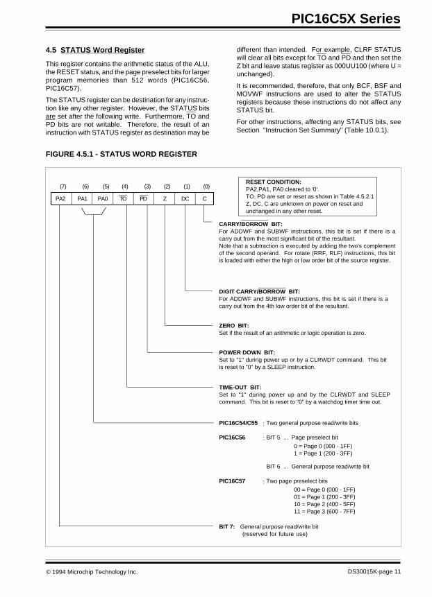
4.5 STATUS Word Register
This register contains the arithmetic status of the ALU,the RESET status, and the page preselect bits for largerprogram memories than 512 words (PIC16C56,PIC16C57).
The STATUS register can be destination for any instruc-tion like any other register. However, the STATUS bitsare set after the following write. Furthermore, TO andPD bits are not writable. Therefore, the result of aninstruction with STATUS register as destination may be
different than intended. For example, CLRF STATUSwill clear all bits except for TO and PD and then set theZ bit and leave status register as 000UU100 (where U =unchanged).
It is recommended, therefore, that only BCF, BSF andMOVWF instructions are used to alter the STATUSregisters because these instructions do not affect anySTATUS bit.
For other instructions, affecting any STATUS bits, seeSection "Instruction Set Summary" (Table 10.0.1).
FIGURE 4.5.1 - STATUS WORD REGISTER
CARRY/BORROW BIT:For ADDWF and SUBWF instructions, this bit is set if there is a carry out from the most significant bit of the resultant.Note that a subtraction is executed by adding the two's complement of the second operand. For rotate (RRF, RLF) instructions, this bit is loaded with either the high or low order bit of the source register.
DIGIT CARRY/BORROW BIT:For ADDWF and SUBWF instructions, this bit is set if there is a carry out from the 4th low order bit of the resultant.
ZERO BIT:Set if the result of an arithmetic or logic operation is zero.
POWER DOWN BIT:Set to "1" during power up or by a CLRWDT command. This bit is reset to "0" by a SLEEP instruction.
TIME-OUT BIT:Set to "1" during power up and by the CLRWDT and SLEEP command. This bit is reset to "0" by a watchdog timer time out.
BIT 7: General purpose read/write bit(reserved for future use)
PIC16C54/C55
PIC16C56
PIC16C57
:
:
:
Two general purpose read/write bits
BIT 5 ... Page preselect bit
BIT 6 ... General purpose read/write bit
Two page preselect bits
0 = Page 0 (000 - 1FF)1 = Page 1 (200 - 3FF)
00 = Page 0 (000 - 1FF)01 = Page 1 (200 - 3FF)10 = Page 2 (400 - 5FF)11 = Page 3 (600 - 7FF)
PA2 PA1 PA0 TO PD Z DC C
(7) (6) (5) (4) (3) (2) (1) (0)RESET CONDITION:PA2,PA1, PA0 cleared to '0'.TO, PD are set or reset as shown in Table 4.5.2.1Z, DC, C are unknown on power on reset and unchanged in any other reset.

PIC16C5X Series
© 1994 Microchip Technology Inc.DS30015K-page 12
TO PD RESET was caused by
0 0 WDT wake-up from SLEEP0 1 WDT time-out (not during SLEEP)1 0 MCLR wake-up from SLEEP1 1 Power-upX X = Low pulse on MCLR input
Note: The PD and TO bit maintain their status (X) until an eventof Table 4.5.2.1 occurs. A low-pulse on the MCLR inputdoes not change the PD and TO status bits.
Event TO PD Remarks
Power-up 1 1WDT Timeout 0 X No effect on PDSLEEP instruction 1 0CLRWDT instruction 1 1
Note: A WDT timeout will occur regardless of the status of the TObit. A SLEEP instruction will be executed, regardless of thestatus of the PD bit. Table 4.5.2.2 reflects the status of PDand TO after the corresponding event.
TABLE 4.5.2.2 - PD/TO STATUS AFTERRESET
4.5.3 PROGRAM PAGE PRESELECT (PIC16C56, PIC16C57 ONLY)
Bits 5-6 of the STATUS register are defined as PAGEaddress bits PA0<1:0>, and are used to preselect aprogram memory page. When executing a GOTO,CALL, or an instruction with PC as destination (e.g.MOVWF PC), PA<1:0> are loaded into bit A<10:9> ofthe program counter, selecting one of the availableprogram memory pages. The direct address specified inthe instruction is only valid within this particular memorypage.
RETLW instructions do not change the page preselectbits.
Upon a RESET condition, PA<2:0> are cleared to "0"s.
4.6 File Select Register (FSR)
PIC16C54/C55/C56
Bits 0-4 select one of the 32 available file registers in theindirect addressing mode (that is, calling the INDFregister in any of the file oriented instructions).
Bits 5-7 of the FSR are read-only and are always read as"one"s.
If no indirect addressing is used, the FSR can be usedas a 5-bit wide general purpose register.
PIC16C57 ONLY
Bits 5 and 6 of the FSR select the current data memorybank (Figure 4.2.1).
The lower 16 bytes of each bank are physically identicaland are always selected when bit 4 of the FSR (in caseof indirect addressing) is "0", or bit 4 of the direct fileregister address of the currently executing instruction is"0" (e.g. MOVWF 08).
Only if bit 4 in the above mentioned cases is "1", bits 5and 6 of the FSR select one of the four available registerbanks with 16 bytes each.
Bit 7 is read-only and is always read as "one."
TABLE 4.5.2.1 - EVENTS AFFECTING PD/TO STATUS BITS
4.5.1 CARRY/BORROW AND DIGIT CARRY/BORROW BITS:
The Carry bit (C) is a carry out in addition operation(ADDWF) and a borrow out in subtract operation(SUBWF).
It is also affected by RRF and RLF instructions. Thefollowing examples explain carry/borrow bit operation:
;SUBWF Example #1;clrf 0x20 ;f(20h)=0movlw 1 ;wreg=1subwf 0x20 ;f(20h)=f(20h)-wreg=0-1=FFh
;Carry=0: Result is negative;;SUBWF Example #2movlw 0xFF ;movwf 0x20 ;f(20h)=FFhclrw ;wreg=0subwf 0x20 ;f(20h)=f(20h)-wreg=FFh-0=FFh
;Carry=1:Result is positive;
The digit carry operates in the same way as the carry bit,i.e. it is a borrow in subtract operation.
4.5.2 TIME OUT AND POWER DOWN STATUS BITS (TO, PD )
The TO and PD bits in the STATUS register can betested to determine if a RESET condition has beencaused by a Watchdog Timer time-out, a power-upcondition, or a wake-up from SLEEP by the WatchdogWimer or MCLR pin.
These STATUS bits are only affected by events listed inTable 4.5.2.1.

© 1994 Microchip Technology Inc. DS30015K-page 13
PIC16C5X Series
5.0 I/O REGISTERS (PORTS)
The I/O registers can be written and read under programcontrol like any other register of the register file. How-ever, "read" instructions (e.g. MOVF PORTB,W) alwaysread the I/O pins, regardless if a pin is defined as "input"or "output." Upon a RESET condition, all I/O ports aredefined as "input" (= high impedance mode) as the I/Ocontrol registers (TRISA, TRISB, TRISC) are all set to"ones."
The execution of a "TRIS f" instruction with correspond-ing "zeros" in the W-register is necessary to define anyof the I/O pins as output.
5.1 PORTA
4-bit I/O register. Low order 4-bits only are used (RA0 -RA3). Bits 4 - 7 are unimplemented and read as "zeros."
5.2 PORTB
8-bit I/O register.
5.3 PORTC
PIC16C55/C57: 8-bit I/O register.
PIC16C54/C56: General purpose register.
5.4 I/O Interfacing
The equivalent circuit for an I/O port bit is shown inFigure 5.4.1. All ports may be used for both input andoutput operations. For input operations these ports arenon-latching. Any input must be present until read by aninput instruction (e.g. MOVF PORTB, W). The outputsare latched and remain unchanged until the output latchis rewritten. To use a port pin as output, the correspond-ing direction control bit (in TRISA, TRISB, TRISC) mustbe set to zero. For use as an input, the correspondingTRIS bit must be "one". Any I/O pin can be programmedindividually as input or output.
FIGURE 5.4.1 - EQUIVALENT CIRCUIT FOR A SINGLE I/O PIN
"READ"
I/OPIN
TO DATA BUS
"WRITE"
FROM DATA
BUS
VDD
Q1
DATALATCH
D
CK
Q
Q
"TRIS f"
FROM W-REGISTER
VSS
Q2
I/OCONTROL
LATCH
D
CK
Q
Q
"RESET"
SET
P
N

PIC16C5X Series
© 1994 Microchip Technology Inc.DS30015K-page 14
5.5.1 BIDIRECTIONAL I/O PORTS
Some instructions operate internally as read followed bywrite operations. The BCF and BSF instructions, forexample, read the entire port into the CPU, execute thebit operation and re-output the result. Caution must beused when these instructions are applied to a port whereone or more pins are used as input/outputs. For ex-ample, a BSF operation on bit 5 of PORTB will cause alleight bits of f6 to be read into the CPU. Then the BSFoperation takes place on bit 5 and PORTB is re-outputto the output latches. If another bit of PORTB is used asa bidirectional I/O pin (say bit 0) and it is defined as aninput at this time, the input signal present on the pin itselfwould be read into the CPU and re-written to the datalatch of this particular pin, overwriting the previouscontent. As long as the pin stays in the input mode, noproblem occurs. However, if bit 0 is switched into outputmode later on, the content of the data latch may now beunknown.
5.5 I/O Programming Considerations A pin actively outputting a "0" or "1" should not be drivenfrom external devices at the same time in order tochange the level on this pin ("wired-or", "wired-and").The resulting high output currents may damage the chip.
5.5.2 SUCCESSIVE OPERATIONS ON I/O PORTS
The actual write to an I/O port happens at the end of aninstruction cycle, whereas for reading, the data must bevalid at the beginning of the instruction cycle (see Figure5.5.2.1). Therefore, care must be exercised if a writefollowed by a read operation is carried out on the sameI/O port. The sequence of instructions should be such toallow the pin voltage to stabilize (load dependent) beforethe next instruction which causes that file to be read intothe CPU is executed. Otherwise, the previous state ofthat pin may be read into the CPU rather than the newstate. When in doubt, it is better to separate theseinstructions with a NOP or an other instruction notaccessing this I/O port.
FIGURE 5.5.2.1 - I/O PORT READ/WRITE TIMING
Q1 Q2 Q3 Q4 Q1 Q2 Q3 Q4 Q1 Q2 Q3 Q4 Q1 Q2 Q3 Q4
RB (7:0)
Port pin sampled here
Note:
This example showswrite to PORTB followed by a read from PORTB. Note that the data setup time = (0.25 TCY - TPD) where TCY = instruction cycle. Therefore, athigher clock frequencies, write followed by a read may be problematic.
PC PC + 1 PC + 2 PC + 3
NOPNOPMOVF PORTB, WRead PORTB
MOVWF PORTBWrite to PORTB
PCInstruction
fetched
TPDExecute MOVWF PORTB
Execute MOVF PORTB, W
Execute NOP

© 1994 Microchip Technology Inc. DS30015K-page 15
PIC16C5X Series
6.0 GENERAL PURPOSE REGISTERS
PIC16C54/C55/C56:
f08h - f1Fh: are general purpose register files.
PIC16C57 only:
f08h - f0Fh: are general purpose register files whichare always selected, independent of bankselect.
f10h - f1Fh: general purpose register files in memorybank 0.
f20h - f2Fh: physically identical to f00 - f0F.f30h - f3Fh: general purpose register files in memory
bank 1.f40h - f4Fh: physically identical to f00 - f0F.f50h - f5Fh: general purpose register files in memory
bank 2.f60h - f6Fh: physically identical to f00 - f0.f70h - f7Fh: general purpose register files in memory
bank 3.
7.0 SPECIAL PURPOSE REGISTERS
7.1 W Working Register
Holds second operand in two operand instructions and/or supports the internal data transfer.
RTS RTE PSA PS2 PS1 PS0
5 4 3 2 1 0
PRESCALER VALUE RTCC RATE WDT RATE
00001111
PRESCALER ASSIGNMENT BIT:0 .... RTCC1 .... WDT
RTCC SIGNAL EDGE:0 .... INCREMENT ON LOW-TO-HIGH TRANSITION ON RTCC PIN1 .... INCREMENT ON HIGH-TO-LOW TRANSITION ON RTCC PIN
RTCC SIGNAL SOURCE:0 .... INTERNAL INSTRUCTION CYCLE CLOCK (CLKOUT)1 .... TRANSITION ON RTCC PIN
00110011
01010101
1 : 21 : 41 : 81 : 161 : 321 : 641 : 1281 : 256
1 : 11 : 21 : 41 : 81 : 161 : 321 : 641 : 128
RESET VALUE: 111111b
FIGURE 7.5.1 - OPTION REGISTER
7.2 TRISA I/O Control Register ForPORTA
Only bits 0 - 3 are available. The corresponding I/O port(f5) is only 4-bit wide.
7.3 TRISB I/O Control Register ForPORTB
7.4 TRISC I/O Control Register ForPORTC
The I/O control registers will be loaded with the contentof the W register by executing of the TRIS f instruction.A "1" in the I/O control register puts the correspondingI/O pin into a high impedance mode. A "0" puts thecontents of file register PORTA, PORTB, or PORTC,respectively, out on the selected I/O pins.These registers are "write-only" and are set to all "ones"upon a RESET condition.
7.5 OPTION Prescaler/RTCC OptionRegister
Defines prescaler assignment (RTCC or WDT), pres-caler value, signal source and signal edge for the RTCC.The OPTION register is "write-only" and is 6-bit wide.By executing the "OPTION" instruction, the contents ofthe "W" register will be transferred to the option register.Upon a RESET condition, the option register is set to all"ones."

PIC16C5X Series
© 1994 Microchip Technology Inc.DS30015K-page 16
8.0 RESET CONDITIONA RESET condition can be caused by applying power tothe chip (power-up), pulling the MCLR input "low", or bya Watchdog Timer timeout. The device will stay inRESET as long as the oscillator start-up timer (OST) isactive or the MCLR input is "low."
The oscillator start-up timer is activated as soon asMCLR input is sensed to be high. This implies that incase of Power-On Reset with MCLR tied to VDD the OSTstarts from power-up. In case of WDT time-out, it willstart at the end of the time-out (since MCLR is high). Incase of MCLR reset, the OST will start when MCLR goeshigh. The nominal OST time-out period is 18ms. SeeSection 13.0 for detailed information on OST and poweron reset.
During a RESET condition the state of the PIC16C5X isdefined as :
• The oscillator is running, or will be started (power-up or wake-up from SLEEP).
• All I/O port pins (RA0 - RA3, RB0 - RB7, RC0 - RC7)are put into the high-impedance state by setting the"TRIS" registers to all "ones" (= input mode).
• The Program Counter is set to all "ones" (1FFh inPIC16C54/55, 3FFh in PIC16C56 and 7FFh inPIC16C57).
• The OPTION register is set to all "ones".• The Watchdog Timer and its prescaler are cleared.• The upper-three bits (page select bits) in the
STATUS Register are cleared to "zero."• "RC" devices only: The "CLKOUT" signal on the
OSC2 pin is held at a"low" level.
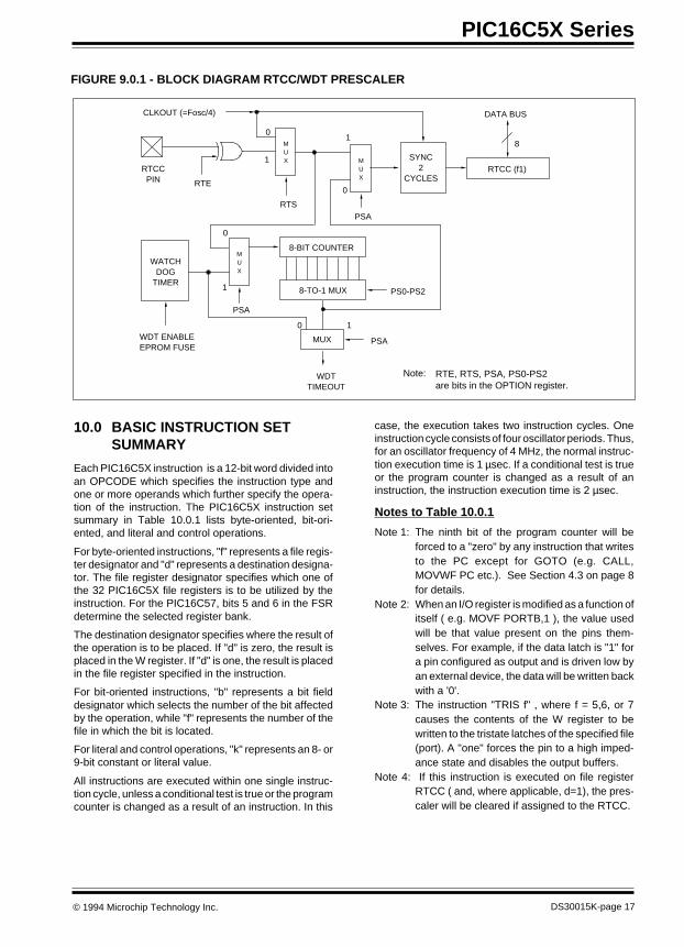
9.0 PRESCALERAn 8-bit counter is available as a prescaler for the RTCC,or as a post-scaler for the Watchdog Timer, respectively(Figure 9.0.1). For simplicity, this counter is being re-ferred to as "prescaler" throughout this data sheet. Notethat there is only one prescaler available which is mutu-ally exclusively shared between the RTCC and theWatchdog Timer. Thus, a prescaler assignment for theRTCC means that there is no prescaler for the WatchdogTimer, and vice-versa.
The PSA and PS0-PS2 bits in the OPTION registerdetermine the prescaler assignment and pre-scale ratio.
When assigned to the RTCC, all instructions writing tothe RTCC (e.g. CLRF RTCC, MOVWF RTCC, BSFRTCC,x ....etc.) will clear the prescaler. When assignedto WDT, a CLRWDT instruction will clear the prescaleralong with the Watchdog Timer.
9.1 Switching Prescaler Assignment
CHANGING PRESCALER FROM RTCC TO WDT
The prescaler assignment is fully under software con-trol, i.e., it can be changed "on the fly" during programexecution. To avoid an unintended device RESET, thefollowing instruction sequence must be executed whenchanging the prescaler assignment from RTCC to WDT:
1. MOVLW B'xx0x0xxx' ; Select internal clock and select new2. OPTION ; prescaler value. If new prescale value
; is = '000' or '001', then select any other; prescale value temporarily.
3. CLRF 1 ; Clear RTCC and prescaler.4. MOVLW B'xxxx1xxx' ; Select WDT, do not change prescale
; value.5. OPTION ;6. CLRWDT ; Clears WDT and prescaler.7. MOVLW B'xxxx1xxx' ; Select new prescale value.8. OPTION ;
Steps 1 and 2 are only required if an external RTCCsource is used. Steps 7 and 8 are necessary only if thedesired prescale value is '000' or '001'.
CHANGING PRESCALER FROM WDT TO RTCC
To change prescaler from WDT to RTCC use the follow-ing sequence:
1. CLRWDT ; Clear WDT and prescaler2. MOVLWB'xxxx0xxx' ; Select RTCC, new prescale value
; and clock source3. OPTION ;
© 1994 Microchip Technology Inc. DS30015K-page 17
PIC16C5X Series
case, the execution takes two instruction cycles. Oneinstruction cycle consists of four oscillator periods. Thus,for an oscillator frequency of 4 MHz, the normal instruc-tion execution time is 1 µsec. If a conditional test is trueor the program counter is changed as a result of aninstruction, the instruction execution time is 2 µsec.
Notes to Table 10.0.1
Note 1: The ninth bit of the program counter will beforced to a "zero" by any instruction that writesto the PC except for GOTO (e.g. CALL,MOVWF PC etc.). See Section 4.3 on page 8for details.
Note 2: When an I/O register is modified as a function ofitself ( e.g. MOVF PORTB,1 ), the value usedwill be that value present on the pins them-selves. For example, if the data latch is "1" fora pin configured as output and is driven low byan external device, the data will be written backwith a '0'.
Note 3: The instruction "TRIS f" , where f = 5,6, or 7causes the contents of the W register to bewritten to the tristate latches of the specified file(port). A "one" forces the pin to a high imped-ance state and disables the output buffers.
Note 4: If this instruction is executed on file registerRTCC ( and, where applicable, d=1), the pres-caler will be cleared if assigned to the RTCC.
10.0 BASIC INSTRUCTION SETSUMMARY
Each PIC16C5X instruction is a 12-bit word divided intoan OPCODE which specifies the instruction type andone or more operands which further specify the opera-tion of the instruction. The PIC16C5X instruction setsummary in Table 10.0.1 lists byte-oriented, bit-ori-ented, and literal and control operations.
For byte-oriented instructions, "f" represents a file regis-ter designator and "d" represents a destination designa-tor. The file register designator specifies which one ofthe 32 PIC16C5X file registers is to be utilized by theinstruction. For the PIC16C57, bits 5 and 6 in the FSRdetermine the selected register bank.
The destination designator specifies where the result ofthe operation is to be placed. If "d" is zero, the result isplaced in the W register. If "d" is one, the result is placedin the file register specified in the instruction.
For bit-oriented instructions, "b" represents a bit fielddesignator which selects the number of the bit affectedby the operation, while "f" represents the number of thefile in which the bit is located.
For literal and control operations, "k" represents an 8- or9-bit constant or literal value.
All instructions are executed within one single instruc-tion cycle, unless a conditional test is true or the programcounter is changed as a result of an instruction. In this
PS0-PS2
RTE
RTS
WATCHDOG
TIMER
WDTTIMEOUT
MUX
0
CLKOUT (=Fosc/4)
MUX
1
PSA
0
SYNC2
CYCLESRTCC (f1)
DATA BUS
8
8-BIT COUNTER
8-TO-1 MUX
MUX
0
PSA
1
WDT ENABLEEPROM FUSE
MUX
0 1
PSA
1RTCCPIN
Note: RTE, RTS, PSA, PS0-PS2are bits in the OPTION register.
FIGURE 9.0.1 - BLOCK DIAGRAM RTCC/WDT PRESCALER

PIC16C5X Series
© 1994 Microchip Technology Inc.DS30015K-page 18
0001 11df ffff 1Cf Add W and f ADDWF f, d W + f → d C,DC,Z 1,2,40001 01df ffff 14f AND W and f ANDWF f, d W & f → d Z 2,40000 011f ffff 06f Clear f CLRF f 0 → f Z 40000 0100 0000 040 Clear W CLRW - 0 → W Z
0010 01df ffff 24f Complement f COMF f, d f → d Z 2,40000 11df ffff 0Cf Decrement f DECF f, d f -1 → d Z 2,40010 11df ffff 2Cf Decrement f,Skip if Zero DECFSZ f, d f - 1 → d, skip if zero None 2,40010 10df ffff 28f Increment f INCF f, d f + 1 → d Z 2,40011 11df ffff 3Cf Increment f,Skip if zero INCFSZ f, d f + 1 → d, skip if zero None 2,40001 00df ffff 10f Inclusive OR W and f IORWF f, d W v f → d Z 2,40010 00df ffff 20f Move f MOVF f, d f → d Z 2,40000 001f ffff 02f Move W to f MOVWF f W → f None 1,40000 0000 0000 000 No Operation NOP - - None0011 01df ffff 34f Rotate left f RLF f, d f(n) → d(n+1), C → d(0), f(7) → C C 2,40011 00df ffff 30f Rotate right f RRF f, d f(n) → d(n-1), C → d(7), f(0) → C C 2,40000 10df ffff 08f Subtract W from f SUBWF f, d f - W → d [f + W + 1 → d] C,DC,Z 1,2,40011 10df ffff 38f Swap halves f SWAPF f, d f(0-3) ↔ f(4-7) → d None 2,40001 10df ffff 18f Exclusive OR W and f XORWF f, d W ⊕ f → d Z 2,4
Instruction-Binary (Hex) Name Mnemonic, Operands Operation Status Affected Notes
0100 bbbf ffff 4bf Bit Clear f BCF f, b 0 → f(b) None 2,40101 bbbf ffff 5bf Bit Set f BSF f, b 1 → f(b) None 2,40110 bbbf ffff 6bf Bit Test f,Skip if Clear BTFSC f, b Test bit (b) in file (f): Skip if clear None0111 bbbf ffff 7bf Bit Test f, Skip if Set BTFSS f, b Test bit (b) in file (f): Skip if set None
Instruction-Binary (Hex) Name Mnemonic, Operands Operation Status Affected Notes
1110 kkkk kkkk Ekk AND Literal and W ANDLW k k & W→ W Z1001 kkkk kkkk 9kk Call subroutine CALL k PC + 1 → Stack, k → PC None 10000 0000 0100 004 Clear Watchdog timer CLRWDT - 0 → WDT (and prescaler, if assigned) TO, PD101k kkkk kkkk Akk Go To address (k is 9 bit) GOTO k k → PC (9 bits) None1101 kkkk kkkk Dkk Incl. OR Literal and W IORLW k k v W → W Z1100 kkkk kkkk Ckk Move Literal to W MOVLW k k → W None0000 0000 0010 002 Load OPTION register OPTION - W → OPTION register None1000 kkkk kkkk 8kk Return,place Literal in W RETLW k k → W, Stack → PC None0000 0000 0011 003 Go into standby mode SLEEP - 0 → WDT, stop oscillator TO, PD0000 0000 0fff 00f Tristate port f TRIS f W→ I/O control register f None 31111 kkkk kkkk Fkk Excl. OR Literal and W XORLW k k ⊕ W → W Z
OPCODE d f(FILE #)
(11-6) (5) (4 - 0)
d = 0 for destination Wd = 1 for destination f
Instruction-Binary (Hex) Name Mnemonic, Operands Operation Status Affected Notes
BYTE -ORIENTED FILE REGISTER OPERATIONS
TABLE 10.0.1 - INSTRUCTION SET SUMMARY
Notes: See previous page
LITERAL AND CONTROL OPERATIONS OPCODE k (LITERAL)
(11-8) (7 - 0)
BIT- ORIENTED FILE REGISTER OPERATIONS OPCODE b(BIT #) f(FILE #)
(11-8) (7-5) (4 - 0)

© 1994 Microchip Technology Inc. DS30015K-page 19
PIC16C5X Series
10.1 Instruction Description
ADDWF ADD W to f
Syntax: ADDWF f,d
Encoding: 0001 11df ffff
Words: 1
Cycles: 1
Operation: (W + f) → d
Status bits: C, DC, Z
Description: Add the contents of the W register toregister “f”. If “d” is 0 the result is storedin the W register. If “d” is 1 the result isstored back in register “f”.
ANDLW AND Literal and W
Syntax: ANDLW k
Encoding: 1110 kkkk kkkk
Words: 1
Cycles: 1
Operation: (W .AND. k) → W
Status bits: Z
Description: The contents of W register are AND’edwith the 8-bit literal “k”. The result isplaced in the W register.
ANDWF AND W with f
Syntax: ANDWF f,d
Encoding: 0001 01df ffff
Words: 1
Cycles: 1
Operation: (W .AND. f) → d
Status bits: Z
Description: AND the W register with register “f”. If “d”is 0 the result is stored in the W register.If “d” is 1 the result is stored back inregister “f”.
BCF Bit Clear f
Syntax: BCF f,b
Encoding: 0100 bbbf ffff
Words: 1
Cycles: 1
Operation: 0 → f(b)
Status bits: None
Description: Bit “b” in register “f” is reset to 0.
BSF Bit Set f
Syntax: BSF f,b
Encoding: 0101 bbbf ffff
Words: 1
Cycles: 1
Operation: 1 → f(b)
Status bits: None
Description: Bit “b” in register “f” is set to 1.
BTFSC Bit Test, skip if Clear
Syntax: BTFSC f,b
Encoding: 0110 bbbf ffff
Words: 1
Cycles: 1(2)
Operation: skip if f(b) = 0
Status bits: None
Description: If bit “b” in register “f” is “0” then the nextinstruction is skipped.
If bit “b” is “0”, the next instruction, fetchedduring the current instruction execution,is discarded and a NOP is executed in-stead making this a two-cycle instruction.
BTFSS Bit Test, skip if Set
Syntax: BTFSS f,b
Encoding: 0111 bbbf ffff
Words: 1
Cycles: 1 (2)
Operation: skip if f(b) = 1
Status bits: None
Description: If bit “b” in register “f” is “1” then the nextinstruction is skipped.
If bit "b" is "1", the next instruction, fetchedduring the current instruction execution,is discarded and a NOP is executed in-stead making this a two-cycle instruction.
CALL Subroutine Call
Syntax: CALL k
Encoding: 1001 kkkk kkkk
Words: 1
Cycles: 2
Operation: PC + 1 → TOS; k → PC<7:0>,'0' → PC<8>, PA2, PA1, PA0 →PC<11:9>;
Status bits: None

PIC16C5X Series
© 1994 Microchip Technology Inc.DS30015K-page 20
Description: Subroutine call. First, return address (PC+ 1) is pushed into the stack. The eight bitvalue is loaded into PC bits <7:0>. PC bit8 is cleared. PA <2:0> bits are loaded intoPC <11:9>. CALL is a two cycle instruc-tion.
CLRF Clear f
Syntax: CLRF f
Encoding: 0000 011f ffff
Words: 1
Cycles: 1
Operation: 00h → f
Status bits: Z
Description: The contents of register “f” are set to 0.
CLRW Clear W Register
Syntax: CLRW
Encoding: 0000 0100 0000
Words: 1
Cycles: 1
Operation: 00h →W
Status bits: Z
Description: W registered is cleared. Zero bit (Z) is set.
CLRWDT Clear Watchdog Timer
Syntax: CLRWDT
Encoding: 0000 0000 0100
Words: 1
Cycles: 1
Operation: 00h →WDT, 0 → WDT prescaler,
Status bits: 1 → TO, 1 → PD
Description: CLRWDT instruction resets the WatchdogTimer.It also resets the prescaler of theWDT. Status bits TO and PD are set.
COMF Complement f
Syntax: COMF f,d
Encoding: 0010 01df ffff
Words: 1
Cycles: 1
Operation: f → d
Status bits: Z
Description: The contents of register “f” are comple-mented. If “d” is 0 the result is stored in W.If “d” is 1 the result is stored back inregister “f”.
DECF Decrement f
Syntax: DECF f,d
Encoding: 0000 11df ffff
Words: 1
Cycles: 1
Operation: (f-1) → d
Status bits: Z
Description: Decrement register “f”. If “d” is 0 the resultis stored in the W register. If “d” is 1 theresult is stored back in register “f”.
DECFSZ Decrement f, skip if 0
Syntax: DECFSZ f,d
Encoding: 0010 11df ffff
Words: 1
Cycles: 1 (2)
Operation: (f - 1) → d; skip if result = 0
Status bits: None
Description: The contents of register “f” are decre-mented. If “d” is 0 the result is placed inthe W register. If “d” is 1 the result isplaced back in register “f”. If the result is0 the next instruction is skipped.
If the result is 0, the next instruction,which is already fetched, is discarded. ANOP is executed instead making it a two-cycle instruction.
GOTO Unconditional Branch
Syntax: GOTO k
Encoding: 101k kkkk kkkk
Words: 1
Cycles: 2
Operation: k → PC<8:0>, PA2, PA1, PA0
→ PC<11:9>;
Status bits: None
Description: The low order nine bits come from theimmediate value. The upper-three bitsare loaded from the PA <2:0> bits in theSTATUS register.
INCF Increment f
Syntax: INCF f,d
Encoding: 0010 10df ffff
Words: 1
Cycles: 1
Operation: (f + 1) → d
Status bits: Z

© 1994 Microchip Technology Inc. DS30015K-page 21
PIC16C5X Series
Description: The contents of register “f” are incre-mented. If “d” is 0 the result is placed inthe W register. If “d” is 1 the result isplaced back in register “f”.
INCFSZ Increment f, skip if 0
Syntax: INCFSZ f,d
Encoding: 0011 11df ffff
Words: 1
Cycles: 1 (2)
Operation: (f + 1) → d, skip if result = 0
Status bits: None
Description: The contents of register “f” are incre-mented. If “d” is 0 the result is placed inthe W register. If “d” is 1 the result isplaced back in register “f”. If the result is0 the next instruction is skipped.
If the result is 0, the next instruction,which is already fetched, is discarded. ANOP is executed instead making it a two-cycle instruction.
IORLW Inclusive OR Literal with W
Syntax: IORLW k
Encoding: 1101 kkkk kkkk
Words: 1
Cycles: 1
Operation: (W .OR. k) → W
Status bits: Z
Description: The contents of the W register are OR’edwith the 8-bit literal “k”. The result isplaced in the W register.
IORWF Inclusive OR W with f
Syntax: IORWF f,d
Encoding: 0001 00df ffff
Words: 1
Cycles: 1
Operation: (W .OR. f) → d
Status bits: Z
Description: Inclusive OR the W register with register“f”. If “d” is 0 the result is stored in the Wregister. If “d” is 1 the result is stored backin register “f”.
MOVF Move f
Syntax: MOVF f,d
Encoding: 0010 00df ffff
Words: 1
Cycles: 1
Operation: (f) → d
Status bits: Z
Description: The contents of register "f" are moved. If"d" is 0 the result is placed in the Wregister. If "d" is 1 the result is placedback in register "f".
MOVLW Move Literal to W
Syntax: MOVLW k
Encoding: 1100 kkkk kkkk
Words: 1
Cycles: 1
Operation: k → W
Status bits: None
Description: The 8-bit literal “k” is loaded into W register.
MOVWF Move W to f
Syntax: MOVWF f
Encoding: 0000 001f ffff
Words: 1
Cycles: 1
Operation: W → f
Status bits: None
Description: Move data from W register to register “f”.
NOP No Operation
Syntax: NOP
Encoding: 0000 0000 0000
Words: 1
Cycles: 1
Operation: No operation
Status bits: None
Description: No operation
OPTION Load Option Register
Syntax: OPTION
Encoding: 0000 0000 0010
Words: 1
Cycles: 1
Operation: W → OPTION;
Status bits: None
Description: The contents of the W register is loaded inthe OPTION register.

DS30015K-page 22
PIC16C5X Series
© 1994 Microchip Technology Inc.
RETLW Return Literal to W
Syntax: RETLW k
Encoding: 1000 kkkk kkkk
Words: 1
Cycles: 2
Operation: k → W; TOS → PC;
Status bits: None
Description: The W register is loaded with the eight bitliteral “k”. The program counter is loadedfrom the top of the stack (the returnaddress). This is a two-cycle instruction.
RLF Rotate Left f through Carry
Syntax: RLF f,d
Encoding: 0011 01df ffff
Words: 1
Cycles: 1
Operation: f<n> → d<n+1>, f<7> → C, C → d<0>;
Status bits: C
Description: The contents of register “f” are rotatedone bit to the left through the Carry Flag.If “d” is 0 the result is placed in the Wregister. If “d” is 1 the result is stored backin register “f”.
RRF Rotate Right f through Carry
Syntax: RRF f,d
Encoding: 0011 00df ffff
Words: 1
Cycles: 1
Operation: f<n> → d<n-1>, f<0> → C, C → d<7>;
Status bits: C
Description: The contents of register “f” are rotatedone bit to the right through the Carry Flag.If “d” is 0 the result is placed in the Wregister. If “d” is 1 the result is placedback in register “f”.
SLEEP
Syntax: SLEEP
Encoding: 0000 0000 0011
Words: 1
Cycles: 1
Operation: 0 → PD, 1 → TO;00h → WDT, 0 → WDT prescaler;
Status bits: TO, PD
Description: The power-down status bit (PD) is cleared.Time-out status bit (TO) is set. WatchdogTimer and its prescaler are cleared.
The processor is put into SLEEP modewith the oscillator stopped. See sectionon SLEEP mode for more details.
SUBWF Subtract W from f
Syntax: SUBWF f,d
Encoding: 0000 10df ffff
Words: 1
Cycles: 1
Operation: (f-W) → d
Status bits: C, DC, Z
;SUBWF Example #1;clrf 0x20 ;f(20h)=0movlw 1 ;wreg=1subwf 0x20 ;f(20h)=f(20h)-wreg=0-1=FFh
;Carry=0; Result is negative;;SUBWF Example #2;movlw 0xFF ;movwf 0x20 ;f(20h)=FFhclrw ;wreg=0subwf 0x20 ;f(20h)=f(20h)-wreg=FFh-0=FFh
;Carry=1:Result is positive;
Description: Subtract (2's complement method) the Wregister from register “f”. If “d” is 0 theresult is stored in the W register. If “d” is1 the result is stored back in register “f”.
SWAPF Swap f
Syntax: SWAPF f,d
Encoding: 0011 10df ffff
Words: 1
Cycles: 1
Operation: f<0:3> → d<4:7>, f<4:7> → d<0:3>;
Status bits: None
Description: The upper and lower nibbles of register “f”are exchanged. If “d” is 0 the result isplaced in W register. If “d” is 1 the resultis placed in register “f”.
TRIS Load TRIS Register
Syntax: TRIS f
Encoding: 0000 0000 0fff
Words: 1
Cycles: 1
Operation: W → TRIS register f;
Status bits: None
Description: TRIS register f (f = 5, 6 or 7) is loaded withthe contents of the W register.

© 1994 Microchip Technology Inc. DS30015K-page 23
PIC16C5X Series
XORLW Exclusive OR literal with W
Syntax: XORLW k
Encoding: 1111 kkkk kkkk
Words: 1
Cycles: 1
Operation: (W .XOR. k) → W
Status bits: Z
Description: The contents of the W register are XOR’edwith the 8-bit literal “k”. The result isplaced in the W register.
XORWF Exclusive OR W with f
Syntax: XORWF f,d
Encoding: 0001 10df ffff
Words: 1
Cycles: 1
Operation: (W .XOR. f) → d
Status bits: Z
Description: Exclusive OR the contents of the W reg-ister with register “f”. If “d” is 0 the resultis stored in the W register. If “d” is 1 theresult is stored back in register “f”.
11.0 WATCHDOG TIMER (WDT)
The Watchdog Timer is realized as a free running on-chip RC oscillator which does not require any externalcomponents. That means that the WDT will run, even ifthe clock on the OSC1/OSC2 pins of the device hasbeen stopped, for example, by execution of a SLEEPinstruction. A WDT timeout generates a device RESETcondition. The WDT can be permanently disabled byprogramming a "zero" into a special EPROM fuse whichis not part of the normal program memory EPROM.
11.1 WDT Period
The WDT has a nominal time-out period of 18ms, (withno prescaler). The time-out periods vary with tempera-ture, VDD and process variations from part to part (seeDC specs). If longer time-out periods are desired, aprescaler with a division ratio of up to 1:128 can beassigned to the WDT under software control by writingto the OPTION register. Thus, time-out periods up to 2.5seconds can be realized.
The "CLRWDT" and "SLEEP" instructions clear theWDT and the prescaler count, if assigned to the WDT,and prevent it from timing out and generating a deviceRESET condition.
The status bit, TO, in the STATUS register, will becleared upon a Watchdog Timer timeout.
The WDT period is a function of the supply voltage,operating temperature, and will also vary from unit to unitdue to variations in the manufacturing process. Pleaserefer to the graphs in Section 18.0 and DC specs formore details.
11.2 WDT Programming Considerations
It should also be taken in account that under worst caseconditions (VDD = Min., Temperature = Max., max. WDTprescaler) it may take several seconds before a WDTtimeout occurs.
12.0 OSCILLATOR CIRCUITS
12.1 Oscillator Types
The PIC16C5X series is available with four differentoscillator options. On windowed devices, a particularoscillator circuit can be selected by programming theconfiguration EPROM accordingly. On OTP and QTPdevices, the oscillator configuration is programmed bythe factory and the parts are tested only to the accordingspecifications.
12.2 Crystal Oscillator
The PIC16C5X-XT, -HS, or LP needs a crystal or ce-ramic resonator connected to the OSC1 and OSC2 pinsto establish oscillation (Figure 12.2.1). XT = Standardcrystal oscillator, HS = High speed crystal oscillator. Theseries resistor RS may be required for the "HS" oscilla-tor, especially at lower than 20 MHz oscillation fre-quency. It may also be required in XT mode with ATstrip-cut type crystals to avoid overdriving.
12.3 RC Oscillator
For timing insensitive applications the "RC" device op-tion offers additional cost savings. The RC oscillatorfrequency is a function of the supply voltage, the resistor(Rext) and capacitor (Cext) values and the operationtemperature. In addition to this, the oscillator frequencywill vary from unit to unit due to normal process param-eter variation. Furthermore, the difference in lead framecapacitance between package types will also affect theoscillation frequency, especially for low Cext values.The user also needs to take into account variation to duetolerance of external R and C components used. Figure12.3.1 shows how the R/C combination is connected tothe PIC16C5X. For Rext values below 2.2 kOhm, theoscillator operation may become unstable, or stop com-pletely. For very high Rext values (e.g. 1 MOhm), theoscillator becomes sensitive to noise, humidity andleakage. Thus, we recommend to keep Rext between 5kOhm and 100 kOhm.
Although the oscillator will operate with no externalcapacitor (Cext = 0 pF), we recommend using valuesabove 20 pF for noise and stability reasons. With no orsmall external capacitance, the oscillation frequencycan vary dramatically due to changes in external capaci-tances, such as PCB trace capacitance or package leadframe capacitance.

DS30015K-page 24
PIC16C5X Series
© 1994 Microchip Technology Inc.
See the table in Section 18.0 for RC frequency variationfrom part to part due to normal process variation. Thevariation is larger for larger R (since leakage currentvariation will affect RC frequency more for large R) andfor smaller C (since variation of input capacitance willaffect RC frequency more).
See characteristics in Section 18.0 for variation of oscil-lator frequency due to VDD for given Rext/Cext values aswell as frequency variation due to operating temperaturefor given R, C and VDD values.
The oscillator frequency, divided by 4, is available on theOSC2/CLKOUT pin, and can be used for test purposesor to synchronize other logic (see Figure 2.2.1 fortiming).
Higher capacitance increases the stability of oscillatorbut also increases the start-up time. These values arefor design guidance only. Since each resonator has itsown characteristics, the user should consult the resona-tor manufacturer for appropriate values of external com-ponents.
FIGURE 12.2.1 - CRYSTAL OPERATION(OR CERAMIC RESONATOR)(HS, XT OR LP TYPES ONLY)
SLEEP
OSC1
PIC16C5X
OSC2
RS
XTAL
TO INTERNAL LOGIC
C1
C2
Rs may be required in HS and XT modes for AT strip-cutcrystals to avoid overdriving. See Tables 12.2.1 and 12.2.2for recommended values of C1, C2 per oscillator type andfrequency.
XT 455 KHz 150 - 330 pF2.0 MHz 20 - 330 pF4.0 MHz 20 - 330 pF
HS 8.0 MHz 20 - 200 pF
Oscillator Resonator Capacitor RangeType Frequency C1 = C2
TABLE 12.2.1 - CAPACITOR SELECTIONFOR CERAMICRESONATORS
FIGURE 12.2.2 - EXTERNAL CLOCK INPUTOPERATION (HS, XT, or LPTYPES ONLY)
OSC1CLOCK FROMEXT. SYSTEM
OSC2OPEN
PIC16C5X
LP 32 KHz 15 pF 15 pFXT 100 KHz 15 - 30 pF 200 - 300 pF
200 KHz 15 - 30 pF 100 - 200 pF455 KHz 15 - 30 pF 15 - 100 pF1 MHz 15 - 30 pF 15 - 30 pF2 MHz 15 pF 15 pF4 MHz 15 pF 15 pF
HS 4 MHz 15 pF 15 pF8 MHz 15 pF 15 pF
20 MHz 15 pF 15 pF
Osc Freq C1 C2Type
Higher capacitance increases the stability of oscillatorbut also increases the start-up time. These values arefor design guidance only. Rs may be required in HSmode as well as XT mode to avoid overdriving crystalswith low drive level specification. Since each crystal hasits own characteristics, the user should consult thecrystal manufacturer for appropriate values of externalcomponents.
FIGURE 12.3.1 - RC OSCILLATOR(RC TYPE ONLY)
OSC2/CLKOUT
Cext
VDD
Rext
VSS
PIC16C5XRC
OSC1
Fosc/4
N
Internalclock
TABLE 12.2.2 - CAPACITOR SELECTION FORCRYSTAL OSCILLATOR

© 1994 Microchip Technology Inc. DS30015K-page 25
PIC16C5X Series
13.0 OSCILLATOR START-UP TIMER(OST)
Oscillator circuits based on crystals or ceramic resona-tors require a certain time after power-up to establish astable oscillation. An on-chip oscillator start-up timer isprovided which keeps the device in a RESET conditionfor approximately 18ms after the voltage on the MCLRpin has reached a logic high (VIHMC) level. Thus,external RC networks connected to the MCLR input arenot required in most cases, allowing for savings in cost-sensitive and/or space restricted applications.
The OST will also be triggered upon a Watchdog Timertimeout. This is particularly important for applicationsusing the WDT to awake the PIC16C5X from SLEEPmode automatically.
The OST is not adequate for low frequency crystalswhich require much longer than 18ms to start-up andstabilize.
13.1 Power-On Reset (POR)
The PIC16C5X incorporates an on chip Power-On Re-set (POR) circuitry which provides internal chip reset formost power-up situations. To use this feature the usermerely needs to tie MCLR pin to VDD. A simplified blockdiagram of the on-chip power on reset circuit is shown inFigure 13.1.4. The Power-On Reset circuit and theoscillator start-up timer circuit are closely related. Onpower-up the reset latch is set and the start-up timer (seeFigure 13.1.4) is reset. The start-up timer begins count-ing once it detects MCLR to be high. After the time-outperiod, which is typically 18ms, it will reset the reset-latch and thus end the on-chip reset signal.
Figures 13.1.5 and 13.1.6 are two power-up situationswith relatively fast rise time on VDD. In Figure 13.1.5,VDD is allowed to rise and stabilize before bringingMCLR high. The chip will actually come out of resettOST ms after MCLR goes high. In Figure 13.1.6, the onchip Power-On Reset feature is being utilized (MCLRand VDD are tied together). The VDD is stable before thestart-up timer times out and there is no problem in gettinga proper reset. Figure 13.1.7 depicts a potentiallyproblematic situation where VDD rises too slowly. In thissituation, when the start-up timer times out, VDD has notreached the VDD (min) value and the chip is, therefore,not guaranteed to function correctly.
To summarize, the on-chip Power-On Reset is guaran-teed to work if the rate of rise of VDD is no slower than0.05 V/ms. It is also necessary that the VDD starts from0V. The on-chip Power-On Reset is also not adequatefor low frequency crystals which require much longerthan 18ms to start-up and stabilize. For such situations,we recommend that external RC circuits are used forlonger Power-On Reset.
FIGURE 13.1.1 - EXTERNAL POWERON RESET CIRCUIT
FIGURE 13.1.2 - BROWN OUT PROTECTIONCIRCUIT
VDD
PIC16C5X
VDD
R1
MCLR
R3
Q1
R2
This brown circuit is less expensive, albeit less accurate. Transistor Q1 turns off when VDD is below a certain level such that:
Notes:1.
VDD •R1
= 0.7 V.R1 + R2
FIGURE 13.1.3 - BROWN OUT PROTECTIONCIRCUIT
VDD
PIC16C5X
VDD
33 K
MCLR
40 K
10 K
Notes:1. This circuit will activate reset when VDD goes
below (VZ + 0.7 V) where VZ = Zener voltage.
R1= 100Ω to 1KΩ will limit any current flowing into MCLR from external capacitor C in the event of MCLR pin breakdown due to ESD or EOS.
R < 40 KΩ must be observed to make sure that voltage drop across R does not exceed 0.2 V (max leakage current spec on MCLR pin is 5 µA). A larger voltage drop will degrade V IH level on MCLR pin.
Notes:External power on reset circuit is required only if VDD power-up slope is too slow or if a low frequency crystal oscillator is being used that need a long start-up time. The diode D helps discharge the capacitor quickly when VDD powers down.
1.
3.
2.
VDD
R
PIC16C5X
MCLR
C
D
R1
DS30015K-page 26
PIC16C5X Series
© 1994 Microchip Technology Inc.
FIGURE 13.1.4 - SIMPLIFIED POWER ON RESET BLOCK DIAGRAM
FIGURE 13.1.5 - USING EXTERNAL RESET INPUT
FIGURE 13.1.6 - USING ON-CHIP POR (FAST VDD RISE TIME)
ON-CHIPRC OSC
POWER-UPDETECT
8-BIT ASYNCHRIPPLE COUNTER(START-UP TIMER)
WDT TIME-OUT
S
R
Q
Q
CHIP RESET
VDD
POR (POWER-ON RESET)
MCLRPIN
RESET
VDD
INTERNAL POR
tOST
MCLR
OST TIME-OUT
INTERNAL RESET
tOST
note 1
Note 1: The tost time-out is invoked every time the chip comes out of reset.
VDD
MCLR
INTERNAL POR
tOST
OST TIME-OUT
INTERNAL RESET

© 1994 Microchip Technology Inc. DS30015K-page 27
PIC16C5X Series
NOTE: Some applications may require external R/Cnetworks on the MCLR pin in order to allow for oscillatorstartup times longer than one OST period. In this case,a WDT wake up from power-down mode is not recom-mended, because a RESET generated by a WDT timeout does not discharge the external capacitor, and thePIC16C5X will be in RESET only for the Oscillator Start-up Timer period.
15.0 CONFIGURATION FUSES
The configuration EPROM consists of four EPROMfuses which are not part of the normal EPROM forprogram storage.
Two are for the selection of the oscillator type, one is theWatchdog Timer enable fuse, and one is the codeprotection fuse.
OTP or QTP devices have the oscillator configurationprogrammed by the factory and the parts are testedaccordingly. The packages are marked with the suffixes"XT", "RC", "HS" or "LP" following the part number toidentify the oscillator type and operating range.
15.1 Customer ID Code
The PIC16C5X series has 16 special EPROM bits whichare not part of the normal program memory. These bitsare available to the user to store an Identifier (ID) code,checksum, or other informative data. They cannot beaccessed during normal program execution.
FIGURE 13.1.7 - USING ON-CHIP POR (SLOW VDD RISE TIME)
14.0 POWER DOWN MODE (SLEEP)
The power-down mode is entered by executing a SLEEPinstruction.
If enabled, the Watchdog Timer will be cleared but keepsrunning, the bit PD in the STATUS register is cleared, theTO bit is set, and the oscillator driver is turned off. TheI/O ports maintain the status they had, before the SLEEPcommand was executed (driving high, low, or hi-imped-ance).
For lowest current consumption in this mode, all I/O pinsshould be either at VDD, or Vss, with no external circuitrydrawing current from the I/O pin. I/O pins that are in theHigh-Z mode should be pulled high or low externally toavoid switching currents caused by floating inputs. TheRTCC input should also be at VDD or Vss for lowestcurrent consumption.
The MCLR pin must be at VIHMC.
14.1 Wake-Up
The device can be awakened by a Watchdog Timertimeout (if it is enabled) or an externally applied "low"pulse at the MCLR pin. In both cases the PIC16C5X willstay in RESET mode for one oscillator start-up timerperiod (triggered from rising edge on MCLR or WDTtimeout) before normal program execution resumes.
The PD bit in the STATUS register, which is set to oneduring power-on , but cleared by the "SLEEP" com-mand, can be used to determine if the processor waspowered up or awakened from the power-down mode(Table 4.5.1.2). The TO bit in the STATUS register canbe used to determine if the "wake up" was caused by anexternal MCLR signal or a Watchdog Timer timeout.
VDD
MCLR
INTERNAL POR
OST TIME-OUT
INTERNAL RESET
0 V V1
5 V
When VDD rises slowly, the internal time-out period expires long before VDD has reached its final value. In this example, the chip will reset properly if, and only if, V1≥ VDDMIN.
tOST

DS30015K-page 28
PIC16C5X Series
© 1994 Microchip Technology Inc.
15.2.1 Verifying a Code-protected Part
When code protected verifying any program memorylocation will read a scrambled output which looks like"00000000XXXX" (binary) where X is 1 or 0. To verify adevice after code protection, follow this procedure:
a. First, program and verify a good device without codeprotecting it.
b. Next, blow its code protection fuse and then load itscontents in a file.
c. Verify any code-protected Part against this file.
15.2 Code Protection
The program code written into the EPROM can beprotected by programming the code protection fuse with"0".
When code protected, the contents of the programEPROM cannot be read out in a way that the programcode can be reconstructed. In addition, all memorylocations starting at 040h and above are protectedagainst programming.
It is still possible to program locations 000h - 03Fh, theID locations and the configuration fuses.
Note that the configuration fuses and the ID bits can stillbe read, even if the code protection logic is active.

© 1994 Microchip Technology Inc. DS30015K-page 29
PIC16C5X Series
16.1 Absolute Maximum Ratings*
Ambient temperature under bias ....... .-55˚C to +125˚C
Storage Temperature ....................... - 65˚C to +150˚CVoltage on any pin with respect to VSS
(except VDD and MCLR) .............. -0.6V to VDD +0.6 VVoltage on VDD with respect to VSS .............. 0 to +7.5 VVoltage on MCLR with respect to VSS
(Note 2) ....................................................... 0 to +14 VTotal power Dissipation (Note 1) .................... 800 mWMax. Current out of VSS pin ............................ 150 mAMax. Current into VDD pin ................................. 50 mAMax. Current into an input pin ........................ ±500 µAInput clamp current, IIK (VI<0 or VI>VDD) ........ ±20 mAOutput clamp current, IOK (V0<0 or V0>VDD) . ±20 mAMax. Output Current sinked by any I/O pin ....... 25 mAMax. Output Current sourced by any I/O pin .... 20 mAMax. Output Current sourced by a singleI/O port (Port A, B, or C) .................................... 40 mAMax. Output Current sinked by a singleI/O port (Port A, B, or C) ..................................... 50mA
16.0 ELECTRICAL CHARACTERISTICS
*Notice: Stresses above those listed under "Maximum Ratings"
may cause permanent damage to the device. This is a stress
rating only and functional operation of the device at those or any
other conditions above those indicated in the operation listings
of this specification is not implied. Exposure to maximum rating
conditions for extended periods may affect device reliability.
Notes: 1. Total power dissipation should not exceed 800mW for the package. Power dissipation iscalculated as follows:Pdis = VDD x IDD - ∑ Ioh + ∑ (VDD-Voh) x Ioh+ ∑(Vol x Iol)
2. Voltage spikes below VSS at the MCLR pin,inducing currents greater than 80mA, maycause latch-up. Thus, a series resistor of 50-100Ω should be used when applying a "low'level to the MCLR pin rather than pulling thispin directly to VSS.
Name Function Description
RA0 - RA3 I/O PORTA Four input/output lines.RB0 - RB7 I/O PORTB Eight input/output lines.RC0 - RC7 I/O PORTC Eight input/output lines, (PIC16C55/C57 only).RTCC Real Time Clock/Counter Schmitt Trigger Input.
Clock input to RTCC register. Must be tied to VSS or VDD ifnot in use to avoid unintended entering of test modes andto reduce current consumption.
MCLR Master Clear Schmitt Trigger Input.A "Low" voltage on this input generates a RESET conditionfor the PIC16C5X microcontroller.A rising voltage triggers the on-chip oscillator start-up timerwhich keeps the chip in RESET mode for about 18ms. Thisinput must be tied directly, or via a pull-up resistor, to VDD.
OSC1 Oscillator (input) "XT", "HS" and "LP" devices: Input terminal for crystal,ceramic resonator, or external clock generator."RC" devices : Driver terminal for external RC combinationto establish oscillation.
OSC2/CLKOUT Oscillator (output) For "XT", "HS" and "LP" devices: Output terminal for crystaland ceramic resonator. Do not connect any other load tothis output. Leave open if external clock generator is used.For "RC" devices : A "CLKOUT" signal with a frequency of1/4 Fosc1 is put out on this pin.
VDD Power supplyVSS GroundN/C No (internal) Connection
TABLE 16.2 - PIN DESCRIPTIONS

DS30015K-page 30
PIC16C5X Series
© 1994 Microchip Technology Inc.
Supply VoltagePIC16C5X-XT VDD 3.0 6.25 V Fosc = DC to 4 MHzPIC16C5X-RC 3.0 6.25 V Fosc = DC to 4 MHzPIC16C5X-HS 4.5 5.5 V Fosc = DC to 20 MHzPIC16C5X-LP 2.5 6.25 V Fosc = DC to 40 KHzRAM Data Retention VDR 1.5 V Device in SLEEP modeVoltage (Note 3)VDD start voltage to VPOR VSS V See Section 13.1 for details on power onguarantee power on reset resetVDD rise rate to guarantee SVDD 0.05* V/ms See Section 13.1 for details on power onpower on resetSupply Current (Note 2)PIC16C5X-XT IDD 1.8 3.3 mA Fosc = 4 MHz, VDD = 5.5VPIC16C5X-RC (Note 5) 1.8 3.3 mA Fosc = 4 MHz , VDD = 5.5VPIC16C5X-HS 4.8 10 mA Fosc =10 MHz, VDD = 5.5V
9.0 20 mA Fosc = 20 MHz, VDD = 5.5VPIC16C5X-LP 15 32 µA Fosc = 32 KHz, VDD=3.0V, WDT disabledPower Down Current(Note 4)PIC16C5X IPD 4 12 µA VDD = 3.0V, WDT enabled
0.6 9 µA VDD = 3.0V, WDT disabled
16.3 DC CHARACTERISTICS: PIC16C5X-RC, XT, HS, LP (Commercial)
Standard Operating Conditions
Operating temperature 0 ≤ TA ≤ +70˚C, unless otherwise stated
Operating voltage VDD = 3.0V to 5.5V unless otherwise stated
DC CHARACTERISTICS,POWER SUPPLY PINS
* These parameters are based on characterization and are not tested.
Note 1: Data in the column labeled "Typical" is based on characterization results at 25˚C. This data is for designguidance only and is not tested for, or guaranteed by Microchip Technology.
Note 2: The supply current is mainly a function of the operating voltage and frequency. Other factors such as busloading, oscillator type, bus rate, internal code execution pattern, and temperature also have an impact on thecurrent consumption.a) The test conditions for all IDD measurements in active operation mode are:OSC1=external square wave, from rail to rail; all I/O pins tristated, pulled to VDD, RT = VDD, MCLR = VDD; WDTenabled/disabled as specified.b) For stand-by current measurements, the conditions are the same, except that the device is in SLEEP mode.
Note 3: This is the limit to which VDD can be lowered in SLEEP mode without losing RAM data.Note 4: The power down current in SLEEP mode does not depend on the oscillator type. Power down current is
measured with the part in SLEEP mode, with all I/O pins in hi-impedence state and tied to VDD and VSS.Note 5: Does not include current through Rext. The current through the resistor can be estimated by the formula
Ir = VDD/2Rext (mA) with Rext in kOhm.
Units ConditionsTyp
(Note 1)Characteristic Sym Min Max

© 1994 Microchip Technology Inc. DS30015K-page 31
PIC16C5X Series
Supply VoltagePIC16C5X-XT VDD 3.0 6.25 V Fosc = DC to 4 MHzPIC16C5X-RC 3.0 6.25 V Fosc = DC to 4 MHzPIC16C5X-HS 4.5 5.5 V Fosc = DC to 20 MHzPIC16C5X-LP 2.5 6.25 V Fosc = DC to 40 KHzRAM Data Retention VDR 1.5 V Device in SLEEP modeVoltage (Note 3)VDD start voltage to VPOR VSS V See section 13.1 for details on power on guarantee power on reset resetVDD rise rate to guarantee SVDD 0.05* V/ms See section 13.1 for details on power onpower on reset resetSupply Current (Note 2)PIC16C5X-XT IDD 1.8 3.3 mA Fosc = 4 MHz, VDD = 5.5VPIC16C5X-RC (Note 5) 1.8 3.3 mA Fosc = 4 MHz, VDD = 5.5VPIC16C5X-HS 4.8 10.0 mA Fosc = 10 MHz, VDD = 5.5V
9.0 20.0 mA Fosc = 20 MHz, VDD = 5.5VPIC16C5X-LP 19 40 µA Fosc = 32 KHz, VDD = 3.0V, WDT disabledPower Down Current(Note 4)PIC16C5X IPD 5 14 µA VDD = 3.0V, WDT enabled
0.8 12 µA VDD = 3.0V, WDT disabled
16.4 DC CHARACTERISTICS: PIC16C5XI-RC, XT, HS, LP (Industrial)
DC CHARACTERISTICS,POWER SUPPLY PINS
Standard Operating Conditions
Operating temperature -40 ≤ TA ≤ +85˚C, unless otherwise stated
Operating voltage VDD = 3.5V to 5.5V unless otherwise stated
* These parameters are based on characterization and are not tested.
Note 1: Data in the column labeled "Typical" is based on characterization results at 25˚C. This data is for designguidance only and is not tested for, or guaranteed by Microchip Technology.
Note 2: The supply current is mainly a function of the operating voltage and frequency. Other factors such as busloading, oscillator type, bus rate, internal code execution pattern, and temperature also have an impact on thecurrent consumption.a) The test conditions for all IDD measurements in active operation mode are:OSC1= external square wave, from rail to rail; all I/O pins tristated, pulled to VDD, RT = VDD, MCLR = VDD; WDTenabled/disabled as specified.b) For stand-by current measurements, the conditions are the same, except that the device is in SLEEP mode.
Note 3: This is the limit to which VDD can be lowered in SLEEP mode without losing RAM data.Note 4: The power down current in SLEEP mode does not depend on the oscillator type. Power down current is
measured with the part in SLEEP mode, with all I/O pins in hi-impedence state and tied to VDD and VSS.Note 5: Does not include current through Rext. The current through the resistor can be estimated by the formula
Ir = VDD/2Rext (mA) with Rext in kOhm.
SymCharacteristic Max Units ConditionsMinTyp
(Note 1)

DS30015K-page 32
PIC16C5X Series
© 1994 Microchip Technology Inc.
Supply VoltagePIC16C5X-XT VDD 3.25 6.0 V Fosc = DC to 4 MHzPIC16C5X-RC 3.25 6.0 V Fosc = DC to 4 MHzPIC16C5X-HS 4.5 5.5 V Fosc = DC to 20 MHzPIC16C5X-LP 2.5 6.0 V Fosc = DC to 40 KHzRAM Data Retention VDR 1.5 V Device in SLEEP modeVoltage (Note 3)VDD start voltage to VPOR VSS V See section 13.1 for details on power on guarantee power on reset resetVDD rise rate to guarantee SVDD 0.05* V/ms See section 13.1 for details on power onpower on reset resetSupply Current (Note 2)PIC16C5X-XT IDD 1.8 3.3 mA Fosc = 4 MHz, VDD = 5.5VPIC16C5X-RC (Note 5) 1.8 3.3 mA Fosc = 4 MHz, VDD = 5.5VPIC16C5X-HS 4.8 10.0 mA Fosc = 10 MHz, VDD = 5.5V
9.0 20.0 mA Fosc = 16 MHz, VDD = 5.5VPIC16C5X-LP 25 55 µA Fosc = 32 KHz, VDD = 3.25V, WDT disabledPower Down Current(Note 4)PIC16C5X IPD 5 22 µA VDD = 3.25V, WDT enabled
0.8 18 µA VDD = 3.25V, WDT disabled
16.5 DC CHARACTERISTICS: PIC16C5XE-RC, XT, HS, LP (Automotive)
DC CHARACTERISTICS,POWER SUPPLY PINS
Characteristic Max ConditionsUnits
Standard Operating Conditions
Operating temperature -40 ≤ TA ≤ +125˚C, unless otherwise stated
Operating voltage VDD = 3.5V to 5.5V unless otherwise stated
Sym Min
* These parameters are based on characterization and are not tested.
Note 1: Data in the column labeled "Typical" is based on characterization results at 25˚C. This data is for designguidance only and is not tested for, or guaranteed by Microchip Technology.
Note 2: The supply current is mainly a function of the operating voltage and frequency. Other factors such as busloading, oscillator type, bus rate, internal code execution pattern, and temperature also have an impact on thecurrent consumption.a) The test conditions for all IDD measurements in active operation mode are:OSC1= external square wave, from rail to rail; all I/O pins tristated, pulled to VDD, RT = VDD, MCLR = VDD; WDTenabled/disabled as specified.b) For stand-by current measurements, the conditions are the same, except that the device is in SLEEP mode.
Note 3: This is the limit to which VDD can be lowered in SLEEP mode without losing RAM data.Note 4: The power down current in SLEEP mode does not depend on the oscillator type. Power down current is
measured with the part in SLEEP mode, with all I/O pins in hi-impedence state and tied to VDD and VSS.Note 5: Does not include current through Rext. The current through the resistor can be estimated by the formula
Ir = VDD/2Rext (mA) with Rext in kOhm.
Typ(Note 1)

© 1994 Microchip Technology Inc. DS30015K-page 33
PIC16C5X Series
Input Low VoltageI/O ports VIL VSS 0.2 VDD V Pin at hi-impedanceMCLR (Schmitt trigger) VSS 0.15 VDD VRTCC (Schmitt trigger) VSS 0.15 VDD VOSC1 (Schmitt trigger) VSS 0.15 VDD V PIC16C5XRC only (Note 5)OSC1 VSS 0.3 VDD V PIC16C5X-XT, HS, LPInput High VoltageI/O ports VIH 0.45 VDD VDD V For all VDD (Note 6)
2.0 VDD V 4.0 V < VDD ≤ 5.5 V (Note 6)0.36 VDD VDD V VDD > 5.5 V
MCLR (Schmitt trigger) 0.85 VDD VDD VRTCC (Schmitt trigger) 0.85 VDD VDD VOSC1 (Schmitt trigger) 0.85 VDD VDD V PIC16C5X-RC only (Note 5)OSC1 0.7 VDD VDD V PIC16C5X-XT, HS, LPInput Leakage Current For V DD ≤ 5.5V(Notes 3, 4)I/O ports IIL -1 0.5 +1 µA VSS ≤ VPIN ≤ VDD,
Pin at hi-impedanceMCLR -5 µA VPIN = VSS + 0.25VMCLR 0.5 +5 µA VPIN = VDD
RTCC -3 0.5 +3 µA VSS ≤ VPIN ≤ VDD
OSC1 -3 0.5 +3 µA VSS ≤ VPIN ≤ VDD ,PIC16C5X-XT, HS, LP
Output Low VoltageI/O Ports VOL 0.6 V IOL = 8.7 mA, VDD = 4.5VOSC2/CLKOUT 0.6 V IOL = 1.6 mA, VDD = 4.5V(PIC16C5X-RC)Output High VoltageI/O Ports (Note 4) VOH VDD-0.7 V IOH = -5.4 mA, VDD = 4.5VOSC2/CLKOUT VDD-0.7 V IOH = -1.0 mA, VDD = 4.5V(PIC16C5X-RC)
16.6 DC CHARACTERISTICS: PIC16C5X-RC, XT, HS, LP (Commercial)PIC16C5XI-RC, XT, HS, LP (Industrial)
DC CHARACTERISTICS,ALL PINS EXCEPT POWER SUPPLY
Standard Operating Conditions (unless otherwise stated)
Operating temperature -40 < TA < +85˚C for industrial
and 0˚C ≤ TA ≤ +70˚C for commercial
Operating voltage VDD range as described in DC spec tables
16.3 and 16.4
Characteristic Sym Min Typ Max Units Conditions (Note 1)
Note 1: Data in the column labeled "Typical" is based on characterization results at 25 C. This data is for design guidanceonly and is not tested for, or guaranteed by Microchip Technology.
Note 2 : Total power dissipation as stated under absolute maximum ratings must not be exceeded.Note 3 : The leakage current on the MCLR pin is strongly dependent on the applied voltage level. The specified levels
represent normal operating conditions. Higher leakage current may be measured at different input voltages.Note 4 : Negative current is defined as coming out of the pin.Note 5 : For PIC16C5XRC devices, the OSC1 pin is a Schmitt trigger input. It is not recommended that the PIC16C5X
be driven with external clock in RC mode.Note 6: The user may use better of the two specifications.

DS30015K-page 34
PIC16C5X Series
© 1994 Microchip Technology Inc.
16.7 DC CHARACTERISTICS: PIC16C5X-RC, XT, HS, LP (Automotive)
Characteristic Sym Min Typ Max Units Conditions (Note 1)
Input Low VoltageI/O ports VIL VSS 0.15 VDD V Pin at high-impedanceMCLR (Schmitt trigger) VSS 0.15 VDD VRTCC (Schmitt trigger) VSS 0.15 VDD VOSC1 (Schmitt trigger) VSS 0.15 VDD V PIC16C5XRC only (Note 5)OSC1 VSS 0.3 VDD V PIC16C5X-XT, HS, LP
Input High VoltageI/O ports VIH 0.45 VDD VDD V For all VDD (Note 6)
2.0 VDD V 4.0 V < VDD ≤ 5.5 V (Note 6)0.36 VDD VDD V VDD > 5.5 V
MCLR (Schmitt trigger) 0.85 VDD VDD VRTCC (Schmitt trigger) 0.85 VDD VDD VOSC1 (Schmitt trigger) 0.85 VDD VDD V PIC16C5X-RC only (Note 5)OSC1 0.7 VDD VDD V PIC16C5X-XT, HS, LP
Input Leakage Current For V DD ≤ 5.5V(Notes 3, 4)I/O ports IIL -1 0.5 +1 µA VSS ≤ VPIN ≤ VDD,
Pin at hi-impedanceMCLR -5 µA VPIN = VSS + 0.25VMCLR 0.5 +5 µA VPIN = VDD
RTCC -3 0.5 +3 µA VSS ≤ VPIN ≤ VDD
OSC1 -3 0.5 +3 µA VSS ≤ VPIN ≤ VDD ,PIC16C5X-XT, HS, LP
Output Low VoltageI/O Ports VOL 0.6 V IOL = 8.7 mA, VDD = 4.5VOSC2/CLKOUT 0.6 V IOL = 1.6 mA, VDD = 4.5V(PIC16C5X-RC)
Output High VoltageI/O Ports (Note 4) VOH VDD-0.7 V IOH = -5.4 mA, VDD = 4.5VOSC2/CLKOUT VDD-0.7 V IOH = -1.0 mA, VDD = 4.5V(PIC16C5X-RC)
DC CHARACTERISTICS,ALL PINS EXCEPT POWER SUPPLY
Standard Operating Conditions (unless otherwise stated)
Operating temperature -40 < TA < +125˚C
Operating voltage VDD range as described in DC spec tables
16.3 and 16.4
Note 1: Data in the column labeled "Typical" is based on characterization results at 25 C. This data is for design guidanceonly and is not tested for, or guaranteed by Microchip Technology.
Note 2 : Total power dissipation as stated under absolute maximum ratings must not be exceeded.Note 3 : The leakage current on the MCLR pin is strongly dependent on the applied voltage level. The specified levels
represent normal operating conditions. Higher leakage current may be measured at different input voltages.Note 4 : Negative current is defined as coming out of the pin.Note 5 : For PIC16C5XRC devices, the OSC1 pin is a Schmitt trigger input. It is not recommended that the PIC16C5X
be driven with external clock in RC mode.Note 6: The user may use better of the two specifications.

© 1994 Microchip Technology Inc. DS30015K-page 35
PIC16C5X Series
16.8 AC CHARACTERISTICS: PIC16C5X-RC, XT, HS, LP (Commercial)PIC16C5XI-RC, XT, HS, LP (Industrial)PIC16C5XI-RC, XT, HS, LP (Automotive)
External CLOCKIN FOSC DC 4 MHz RC modeFrequency (Note 2) DC 4 MHz XT mode
DC 20 MHz HS mode (Com/Ind)DC 16 MHz HS mode (Automotive)DC 40 KHz LP mode
Oscillator Frequency FOSC DC 4 MHz RC mode(Note 2) 0.1 4 MHz XT mode
4 20 MHz HS mode (Com/Ind)4 16 MHz HS mode (Automotive)DC 40 KHz LP mode
Instruction Cycle Time TCY 1.0 4/FOSC DC µs RC mode(Note 2) 1.0 DC µs XT mode
0.2 DC µs HS mode100 DC µs LP mode
External Clock in Timing(Note 4)Clock in (OSC1) High or Low TimeXT oscillator type TCKHLXT 50* nsLP oscillator type TCKHLLP 2* µsHS oscillator type TCKHLHS 20* nsClock in (OSC1) Rise or Fall TimeXT oscillator type TCKRFXT 25* nsLP oscillator type TCKRFLP 50* nsHS oscillator type TCKRFHS 25* nsRESET TimingMCLR Pulse Width (low) TMCL 100* nsRTCC Input Timing, No PrescalerRTCC High Pulse Width TRTH 0.5 TCY+ 20* ns Note 3RTCC Low Pulse Width TRTL 0.5 TCY+ 20* ns Note 3RTCC Input Timing, With PrescalerRTCC High Pulse Width TRTH 10* ns Note 3RTCC Low Pulse Width TRTL 10* ns Note 3RTCC Period TRTP ns Note 3. Where N = prescale
value (2,4, ..., 256)Watchdog Timer Timeout Period(No Prescaler) TWDT 9* 18* 30* ms VDD = 5.0VOscillation Start-up Timer Period TOST 9* 18* 30* ms VDD = 5.0VI/O TimingI/O Pin Input Valid BeforeCLKOUT↑ (RC Mode) TDS 0.25 TCY+ 30* nsI/O Pin Input Hold AfterCLKOUT↑ (RC Mode) TDH 0* nsI/O Pin Output Valid AfterCLKOUT↓ (RC Mode) TPD 40* ns
Characteristic Sym Min Typ Max Units Conditions (Note 1)
AC CHARACTERISTICS Standard Operating Conditions (unless otherwise stated)Operating temperature TA = -40˚C to +85˚C (industrial),TA = -40˚C to +125˚C (automotive) and 0˚C ≤ TA ≤ +70˚C (commercial)Operating voltage VDD range as described in DC spec tables 16.3 and 16.4
* Guaranteed by characterization, but not tested. (Notes on next page)
TCY + 40N
*

DS30015K-page 36
PIC16C5X Series
© 1994 Microchip Technology Inc.
NOTES TO TABLE 16.8: result in an unstable oscillator operation and/or higher than ex-pected current consumption. All devices are tested to operate at"min." values with an external clock applied to the OSC1 pin.When an external clock input is used, the "Max." cycle time limitis "DC" (no clock) for all devices.
3. For a detailed explanation of RTCC input clock requirements seesection 4.2.1.
4. Clock-in high-time is the duration for which clock input is at VIHOSCor higher.Clock-in low-time is the duration for which clock input is at VILOSCor lower.
16.9 Electrical Structure of Pins
FIGURE 16.9.1 - ELECTRICALSTRUCTURE OF I/O PINS (RA, RB, RC)
FIGURE 16.9.2 - ELECTRICALSTRUCTURE OF MCLR AND RTCC PINS
Input buffer
N
VDD
P
VSS
I/O pin
VSS
Rin
Schmitt trigger Input buffer
VSS
MCLR, RTCC N
VSS
Rin
Notes to Figures 16.9.1 and 16.9.2: The diodes and the grounded gate (or output driver) NMOS device are carefully designed to protect against ESD(Electrostatic discharge) and EOS (Electrical overstress). Rin is a small resistance to further protect the input buffer from ESD.
FIGURE 17.0.3 - INPUT/OUTPUT TIMING FOR I/O PORTS (PIC16C5XRC*)
T1
OUTPUTHIGH - Z
INPUT
TdhTds
Tcy
Tpd
* The CLKOUT output is available only on PIC16C5XRC devices.
OSC2/CLKOUT
Tpd
VALID
FIGURE 17.0.2 - OSCILLATOR START-UP TIMING (PIC16C5XRC)
FIGURE 17.0.1 - RTCC TIMING
T1Tost
VIHMC
TcyMCLR
T1
CLKOUT
DEVICEFUNCTION
RESET FETCH 1. INSTRUCTIONEXECUTE "FORCED" NOP
FETCH 2. INSTRUCTIONEXECUTE 1. INSTRUCTION
Tcy
17.0 TIMING DIAGRAMS
1. Data in the column labeled "Typical" is based on characterizationresults at 25˚C. This data is for design guidance only and is nottested for, or guaranteed by Microchip Technology.
2. Instruction cycle period (Tcy) equals four times the input oscillatortime base period.All specified values are based on characterization data for thatparticular oscillator type under standard operating conditions withthe device executing code. Exceeding these specified limits may
TRTH TRTL
RTCC
VIH
TRTP
VIL

© 1994 Microchip Technology Inc. DS30015K-page 37
PIC16C5X Series
18.0 DC AND AC CHARACTERISTICS GRAPHS/TABLES:
The graphs and tables provided in this section are fordesign guidance and are not tested or guaranteed. Insome graphs or tables the data presented are outsidespecified operating range (e.g. outside specified VDD
range). This is for information only and devices areguaranteed to operate properly only within the specifiedrange.
The data presented in this section is a statistical sum-mary of data collected on units from different lots over aperiod of time. 'Typical' represents the mean of thedistribution while 'max' or 'min' represents (mean + 3σ)and (mean - 3σ) respectively where σ is standarddeviation.
FIGURE 18.0.1 - TYPICAL RC OSCILLATORFREQUENCY vs.TEMPERATURE
FIGURE 18.0.2 - TYPICAL RC OSCILLATORFREQUENCY vs VDD*
FIGURE 18.0.3 - TYPICAL RC OSCILLATORFREQUENCY vs VDD*
0
0.2
0.4
0.6
0.8
1.0
1.2
1.4
1.6
1.8
Fre
q. (
Mhz
)
3.0 3.5 4.0 4.5 5.0 5.5 6.0
VDD (Volts)
R=3.3k
R=5k
R=10k
R=100k
FoscFosc (25˚C)
1.08
1.06
1.04
1.02
1.00
0.98
0.96
0.94
0.92
0 10 200.90
7040 50 60
T(˚C)
30
FREQUENCY NORMALIZED TO +25˚C
Rext ≥ 10KΩCext = 100pF
VDD = 5.5V
VDD = 3.5V
0
0.5
1.0
1.5
2.0
2.5
3.0
3.5
4.0
4.5
5.0
3.0 3.5 4.0 4.5 5.0 5.5 6.0
Fos
c (M
hz)
VDD (Volts)
5.5
Cext = 20pF, T = 25˚C
R=100k
R=10k
R=5k
R=3.3k
* Measured on DIP packages. * Measured on DIP packages.

DS30015K-page 38
PIC16C5X Series
© 1994 Microchip Technology Inc.
20pF 3.3k 4.973 MHz ± 27%
5k 3.82 MHz ± 21%
10k 2.22 MHz ± 21%
100k 262.15 KHz ± 31%
100pF 3.3k 1.63 MHz ± 13%
5k 1.19 MHz ± 13%
10k 648.64 KHz ± 18%
100k 71.56 KHz ± 25%
300pF 3.3k 660.0 KHz ± 10%
5k 484.1 KHz ± 14%
10k 267.63 KHz ± 15%
100k 29.44 KHz ± 19%
FIGURE 18.0.4 - TYPICAL RC OSCILLATORFREQUENCY vs VDD*
Cext Rext Average
Fosc @ 5V, 25˚C
TABLE 18.0.1 - RC OSCILLATORFREQUENCIES*
0
100
200
300
400
500
600
700
800
3.5 4.0 4.5 5.0 5.5 6.0
Fos
c (K
hz)
VDD (Volts)
3.0
R=3.3k
R=5k
R=10k
R=100k
The percentage variation indicated here is part to partvariation due to normal process distribution. The varia-tion indicated is ±3 standard deviation from averagevalue for VDD = 5V.
* Measured on DIP packages.
* Measured on DIP packages.
FIGURE 18.0.6 - TYPICAL Ipd vs V DD
WATCHDOG ENABLED 25˚CFIGURE 18.0.5 - TYPICAL Ipd vs V DD
WATCHDOG DISABLED 25˚C
0
0.5
1
1.5
2
2.5
2.5 3.0 3.5 4.0 4.5 5.0 5.5 6.0
Ipd
(uA
)
VDD (Volts)
0
2
4
6
8
10
12
14
16
18
Ipd
(uA
)
2.5 3.0 3.5 4.0 4.5 5.0 5.5 6.0
VDD (Volts)

© 1994 Microchip Technology Inc. DS30015K-page 39
PIC16C5X Series
FIGURE 18.0.7 - MAXIMUM Ipd vs V DD
WATCHDOG DISABLEDFIGURE 18.0.8 - MAXIMUM Ipd vs V DD
WATCHDOG ENABLED*
* IPD, with watchdog timer enabled, has two components: The leakage current which increases with higher temperature and theoperating current of the watchdog timer logic which increases with lower temperature. At -40˚C, the latter dominates explaining theapparently anomalous behavior.
FIGURE 18.0.9 - VTH (INPUT THRESHOLD VOLTAGE) OF I/O PINS vs V DD
2.00VTH (Input threshold voltage) of I/O pins
1.80
1.60
1.40
1.20
1.00
0.80
0.602.5 3.0 3.5 4.0 4.5 5.0 5.5 6.0
VDD (volts)
VT
H (
volts
)
Max (-40˚C to 85˚C)
25˚C, TYP
Min (-40˚C to 85˚C)
0
1
10
100
Ipd
(uA
)
2.5 3.0 3.5 4.0 4.5 5.0 5.5 6.0VDD (Volts)
85
6.5 7.0
Temp. (˚C) = 125
85
70
0
-40
-55
0
10
20
30
40
50
60
Ipd
(uA
)
2.5 3.0 3.5 4.0 4.5 5.0 5.5 6.0VDD (Volts)
6.5 7.0
070
85
-40
-55
125
Temp. (˚C)

DS30015K-page 40
PIC16C5X Series
© 1994 Microchip Technology Inc.
FIGURE 18.0.10 - VIH, VIL OF MCLR, RTCC AND OSC1 (IN RC MODE) vs V DD
FIGURE 18.0.11 - VTH (INPUT THRESHOLD VOLTAGE) OF OSC1 INPUT (IN XT, HS, AND LPMODES) vs VDD
VIH
, VIL
(vol
ts)
0.00
4.50
4.00
3.50
3.00
2.50
2.00
1.50
1.00
0.50
2.5 3.0 3.5 4.0 4.5 5.0 5.5 6.0VDD (volts)
VIH, max (-40˚C to 85˚C)
VIH, min (-40˚C to 85˚C)
VIL, max (-40˚C to 85˚C)
VIL, TYP, 25˚C
VIL, min (-40˚C to 85˚C)
Note: These input pins have Schmitt trigger input buffer.
VIH, TYP, 25˚C
2.5 3.0 3.5 4.0 4.5 5.0 5.5 6.0VDD (volts)
VT
H (
volts
)
1.20
1.40
1.60
1.80
2.00
2.20
2.40
2.60
2.80
3.00
3.20
3.40
1.00
Min (-40˚C to 85˚C)
Max (-40˚C to 85˚C)
25˚C, TYP
© 1994 Microchip Technology Inc. DS30015K-page 41
PIC16C5X Series
FIGURE 18.0.12 - TYPICAL IDD vs FREQ (EXT CLOCK, 25˚C)
FIGURE 18.0.13 - MAXIMUM IDD vs FREQ (EXT CLOCK, -40˚ to +85˚C)
IDD (m
A)
10
1.0
0.1
0.0110K 100K 1M 10M 100M
External Clock freq (Hz)
5.55.04.54.03.5
3.0
6.07.0
2.5
IDD (m
A)
10
1.0
0.1
0.0110K 100K 1M 10M 100M
External Clock freq (Hz)
5.55.04.54.0
3.5
3.0
6.06.5
7.0
2.5

DS30015K-page 42
PIC16C5X Series
© 1994 Microchip Technology Inc.
FIGURE 18.0.16 - Transconductance (gm) ofHS Oscillator vs V DD
FIGURE 18.0.15 - WDT Timer Time-out Periodvs VDD
FIGURE 18.0.14 - MAXIMUM IDD vs FREQ (EXT CLOCK, -55˚ to +125˚C)ID
D (m
A)
10
1
0.1
10K 100K 1M 10M
External Clock freq (Hz)
0.01
7.0
6.0
5.04.03.02.5
10.0
35.0
40.0
45.0
50.0
2 3 4 5 6
WD
T p
erio
d (m
s)
VDD (Volts)
15.0
20.0
25.0
30.0
5.07
Max, 85˚C
Max, 70˚C
Typ, 25˚C
Min, 0˚C
Min, -40˚C
1000
6000
7000
8000
9000
2 3 4 5 6 7
gm (
µA/V
)
VDD (Volts)
2000
3000
4000
5000
0
Min, 85˚C
Typ, 25˚C
Max
, -40
˚C

© 1994 Microchip Technology Inc. DS30015K-page 43
PIC16C5X Series
FIGURE 18.0.18 - Transconductance (gm) ofXT Oscillator vs V DD
FIGURE 18.0.17 - Transconductance (gm) ofLP Oscillator vs V DD
FIGURE 18.0.19 - IOH vs VOH, VDD = 3V FIGURE 18.0.20 - IOH vs VOH, VDD = 5V
IOH
(m
A)
-40
-30
-20
-10
0
Min @ 85˚C
Typ
@ 2
5˚C
Max
@ -4
0˚C
1.5 2 2.5 3 3.5 4 4.5 5VOH (Volts)
10.0
35.0
40.0
45.0
2 3 4 5 6
gm (
µA/V
)
VDD (Volts)
15.0
20.0
25.0
30.0
5.0
70.0
Max
, -40
˚C
Typ, 2
5˚C
Min, 85˚C
0
2000
2500
2 3 4 5 6
gm (
µA/V
)
VDD (Volts)
500
1000
1500
7
Max, -40˚C
Typ, 25˚C
Min, 85˚C
IOH
(m
A)
VOH (Volts)
-25
-20
-15
-10
-5
0
0 0.5 1 1.5 2 2.5 3
Typ @25˚C
Max @ -40˚C
Min @ +85˚C

DS30015K-page 44
PIC16C5X Series
© 1994 Microchip Technology Inc.
FIGURE 18.0.21 - IOL vs VOL, VDD = 3V FIGURE 18.0.22 - IOL vs VOL, VDD = 5V
RA port 5.0 4.3RB port 5.0 4.3MCLR 17.0 17.0OSC1 4.0 3.5OSC2/CLKOUT 4.3 3.5RTCC 3.2 2.8
* All capacitance values are typical at 25˚C and mea-sured at 1 MHz. A part to part variation of ±25% (threestandard deviations) should be taken into account.
Pin NameTypical Capacitance (pF)
18L SOIC18L PDIP
TABLE 18.0.2 - INPUT CAPACITANCE FORPIC16C54/56 *
Pin NameTypical Capacitance (pF)
28L SOIC
TABLE 18.0.3 - INPUT CAPACITANCE FORPIC16C55/57 *
28L PDIP(600 mil)
RA port 5.2 4.8RB port 5.6 4.7RC port 5.0 4.1MCLR 17.0 17.0OSC1 6.6 3.5OSC2/CLKOUT 4.6 3.5RTCC 4.5 3.5
IOL
(mA
)
VOL (Volts)
0
5
10
15
20
25
30
35
40
45
0 0.5 1 1.5 2 2.5 3
Typ @ 25˚C
Max @ -40˚C
Min @ +85˚C
IOL
(mA
)
VOL (Volts)
0
10
20
30
40
50
60
70
80
90
0 0.5 1 1.5 2 2.5 3
Max @ -40˚C
Typ @ 25˚C
Min @ 85˚C

© 1994 Microchip Technology Inc. DS30015K-page 45
PIC16C5X Series
Min
0°
–
0.381
3.048
0.3556
1.524
0.203
22.479
20.320
7.620
6.096
2.4892
7.620
7.874
3.048
18
0.889
0.127
Symbol
α
A
A1
A2
B
B1
C
D
D1
E
E1
e1
eA
eB
L
N
S
S1
Max
10°
4.064
–
3.810
0.5588
1.524
0.381
23.495
20.320
8.255
7.112
2.5908
7.620
9.906
3.556
18
–
–
Max
10°
0.160
–
0.150
0.022
0.060
0.015
0.925
0.800
0.325
0.280
0.102
0.300
0.390
0.140
18
–
–
Min
0°
–
0.015
0.120
0.014
0.060
0.008
0.885
0.800
0.300
0.240
0.098
0.300
0.310
0.120
18
0.035
0.005
Notes
Reference
Typical
Reference
Typical
Reference
Notes
Reference
Typical
Reference
Typical
Reference
Millimeters Inches
Package Group: Plastic Dual In-line (PLA)
Pin No. 1IndicatorArea
N
EE1
SeatingPlane
BasePlane
BD1
SD
B1 e1
S1
L
AA1 A2
α C
eA
eB
19.0 PACKAGING INFORMATION
19.1 Package Type: 18-Lead Plastic Dual In-line (300 mil)

DS30015K-page 46
PIC16C5X Series
© 1994 Microchip Technology Inc.
19.2 Package Type: 28-Lead Dual In-line Plastic (600 mil)
Min
0°
–
0.508
3.175
0.3556
1.270
0.2032
35.052
33.020
15.240
12.827
2.4892
15.240
15.240
2.921
28
0.889
0.508
Symbol
α
A
A1
A2
B
B1
C
D
D1
E
E1
e1
eA
eB
L
N
S
S1
Max
10°
5.080
–
4.064
0.5588
1.778
0.381
37.084
33.020
15.875
13.970
2.5908
15.240
17.272
3.683
28
–
–
Max
10°
0.200
–
0.160
0.022
0.070
0.015
1.460
1.300
0.625
0.550
0.102
0.600
0.680
0.145
28
–
–
Min
0°
–
0.020
0.125
0.014
0.050
0.008
1.380
1.300
0.600
0.505
0.098
0.600
0.600
0.115
28
0.035
0.020
Notes
Typical
Typical
Reference
Typical
Reference
Notes
Typical
Typical
Reference
Typical
Reference
Millimeters Inches
Package Group: Plastic Dual-In-Line (PLA)
Pin No. 1IndicatorArea
EE1
N
SeatingPlane
BasePlane
B
SD
B1 e1
S1
L
AA1 A2
D1
α C
eA
eB
19.0 PACKAGING INFORMATION (CONT.)

© 1994 Microchip Technology Inc. DS30015K-page 47
PIC16C5X Series
19.3 Package Type: 28-Lead Dual In-line Plastic (300 mil)
Min
0°
3.6322
.381
3.175
.4064
1.016
.762
.2032
.2032
34.163
33.02
7.874
7.112
2.54
7.874
8.128
3.175
28
.5842
Symbol
α
A
A1
A2
B
B1
B2
B3
C
D
D1
E
E1
e1
eA
eB
L
N
S
Max
10°
4.572
–
3.556
0.5588
1.651
1.016
.508
.3302
35.179
33.02
8.382
7.493
2.54
7.874
9.652
3.683
-
1.2192
Max
10°
.180
–
.140
.022
.065
.040
.020
.013
1.395
1.300
.330
.295
.100
.310
.380
.145
-
.048
Min
0°
.143
.015
.125
.016
.040
.030
.008
.008
1.385
1.300
.310
.280
.100
.310
.320
.125
28
.023
Notes
Typical
4 places
4 places
Typical
Reference
Typical
Reference
Notes
Typical
4 places
4 places
Typical
Reference
Typical
Reference
Millimeters Inches
Pin No. 1IndicatorArea
EE1
N
SeatingPlane
BasePlane
SD
e1
L
AA1 A2
D1
α C
eA
eB
Detail A
Detail A
B1B2
BB3
Package Group: Plastic Dual-In-Line (PLA)
19.0 PACKAGING INFORMATION (CONT.)

DS30015K-page 48
PIC16C5X Series
© 1994 Microchip Technology Inc.
19.4 Package Type: 18-Lead Plastic Surface Mount (SOIC - Wide, 300 mil Body)
Min
0°
2.3622
0.1016
0.3556
0.2413
11.3538
7.4168
1.270
10.0076
0.381
0.4064
18
–
Symbol
α
A
A1
B
C
D
E
e
H
h
L
N
CP
Max
8°
2.6416
0.29972
0.4826
0.3175
11.7348
7.5946
1.270
10.6426
0.762
1.143
18
0.1016
Max
8°
0.104
0.0118
0.019
0.0125
0.462
0.299
0.050
0.419
0.030
0.045
18
0.004
Min
0°
0.093
0.004
0.014
0.0095
0.447
0.292
0.050
0.394
0.015
0.016
18
–
Notes
Reference
Notes
Reference
Millimeters Inches
Package Group: Plastic SOIC (SO)
Seating Plane
AA1
D
Base Plane
CP
B
E H
e
Chamferh x 45°
N
IndexArea
1 2 3
h x 45°
α C
L
h x 45°
α C
L
19.0 PACKAGING INFORMATION (CONT.)

© 1994 Microchip Technology Inc. DS30015K-page 49
PIC16C5X Series
19.5 Package Type: 28-Lead Plastic Surface Mount (SOIC - Wide, 300 mil Body)
Min
0°
2.3622
0.1016
0.3556
0.2413
17.7038
7.4168
1.270
10.0076
0.381
0.4064
28
–
Symbol
α
A
A1
B
C
D
E
e
H
h
L
N
CP
Max
8°
2.6416
0.2997
0.4826
0.3175
18.0848
7.5946
1.270
10.6426
0.762
1.143
28
0.1016
Max
8°
0.104
0.0118
0.019
0.0125
0.712
0.299
0.050
0.419
0.030
0.045
28
0.004
Min
0°
0.093
0.004
0.014
0.0095
0.697
0.292
0.050
0.394
0.015
0.016
28
–
Notes
Typical
Notes
Typical
Millimeters Inches
Package Group: Plastic SOIC (SO)
Seating Plane
AA1
D
Base Plane
CP
B
E H
e
Chamferh x 45°
N
IndexArea
1 2 3
h x 45°
α C
L
h x 45°
α C
L
19.0 PACKAGING INFORMATION (CONT.)

DS30015K-page 50
PIC16C5X Series
© 1994 Microchip Technology Inc.
19.6 Package Type: 20-Lead Plastic Surface Mount
(SSOP - 209 mil Body 5.30mm)
19.0 PACKAGING INFORMATION (CONT.)
MillimetersMin0°
1.730.050.250.137.075.200.657.650.5520-
SymbolαAA1
BCDEeHLN
CP
Max8°
1.990.210.380.227.335.380.657.900.9520
0.1016
Max8°
0.0780.0080.0150.0090.2890.2120.02560.3110.037
200.004
Min0°
0.0680.0020.0100.0050.2780.2050.02560.3010.022
20-
Notes
Reference
Notes
Reference
InchesPackage Group: Plastic SSOP
e A
D A1
B
HE
Base plane
Index area
12 3
Seating plane
L
α C
N
CP

© 1994 Microchip Technology Inc. DS30015K-page 51
PIC16C5X Series
19.7 Package Type: 28-Lead Plastic Surface Mount
(SSOP - 209 mil Body 5.30mm)
19.0 PACKAGING INFORMATION (CONT.)
HE
e A
D
Base plane
B
Index area
N
123
CP
Seating plane
L
α C
A1
MillimetersMin0°
1.730.050.250.1310.075.200.657.650.5528-
SymbolαAA1
BCDEeHLN
CP
Max8°
1.990.210.380.2210.335.380.657.900.9528
0.1016
Max8°
0.0780.0080.0150.0090.4070.212
0.02560.3110.037
280.004
Min0°
0.0680.0020.0100.0050.3960.2050.02560.3010.022
28-
Notes
Reference
Notes
Reference
InchesPackage Group: Plastic SSOP

DS30015K-page 52
PIC16C5X Series
© 1994 Microchip Technology Inc.
19.0 PACKAGING INFORMATION (CONT.)
Legend: MM...M XX...X AA BB C D E
Microchip part number information Customer specific information* Year code (last 2 digits of calendar year) Week code (week of January 1 is week '01') Facility code of the plant at which wafer is manufactured.
MMMMMMMMMMMMXXX
AABB CDEMMMMMMMMXXXXXXX
18L PDIP
MMMMMMMMM
AABB CDE
18L SOIC
MMMMMMMMM
XXXXXXXXXXXXXXXXXXXX
AABB CDE
28L SOIC
MMMMMMMMMMMMMMMMMMXX
C = Chandler, Arizona, U.S.A. Mask revision number Assembly code of the plant or country of origin in which part was assembled.
PIC16C56-
9123 CBARCI/P456
XTI/S0218
9118 CDK
PIC16C54-
9051 CBK
PIC16C57-XT/SO
Note: In the event the full Microchip part number can not be marked on one line, it will be carried over to the next line thus limiting the number of available characters for customer specific information.
Example
Example
Example
* Standard OTP marking consists of Microchip part number, year code, week code, facility code, mask rev #, and assembly code. For OTP marking beyond this, certain price adders apply. Please check with your Microchip Sales Office. For QTP devices, any special marking adders are incuded in QTP price.
XXXXXXXXXXXXXXX
AABB CDEXXXXXXXXXXXXXXX
28L PDIP (.300 mil)
PIC16C56-
9123 CBARCI/P456
Example
XXXXXXXXXXXX
AABB CDE
28L SSOP
9225 CBK
PIC16C57-XT
Example
XXXXXXXXXXXX
AABB CDE
20L SSOP
XXXXXXXX
XTI/218
9051 CBP
PIC16C54
Example
XXXXXXXX
19.8 Package Marking Information

© 1994 Microchip Technology Inc. DS30015K-page 53
PIC16C5X Series
19.8 Package Marking Information (Cont.)
PIC16C57
9038 CBA
Legend: MM...M XX...X AA BB C D E
Microchip part number information Customer specific information* Year code (last 2 digits of calendar year) Week code (week of January 1 is week '01') Facility code of the plant at which wafer is manufactured.
PIC16C54
9101 CBA
PIC16C55-
9042 CDA
XTI/P126
C = Chandler, Arizona, U.S.A. Mask revision number Assembly code of the plant or country of origin in which part was assembled.
MMMMMMMMMM MMMMMM
AABB CDE
28L Cerdip
MMMMMMMM
AABB CDE
18L Cerdip
MMMMMMMM
MMMMMMMMMMMMXXX
AABB CDE
MMMMMMMMXXXXXXXXXXXXXXXXXXXXXX
28L PDIP (.600 mil)
Note: In the event the full Microchip part number can not be marked on one line, it will be carried over to the next line thus limiting the number of available characters for customer specific information.
Example
Example
Example
* Standard OTP marking consists of Microchip part number, year code, week code, facility code, mask rev #, and assembly code. For OTP marking beyond this, certain price adders apply. Please check with your Microchip Sales Office. For QTP devices, any special marking adders are included in QTP price.
* Standard OTP marking consists of Microchip part number, year code, week code,facility code, mask rev #, and assembly code. For OTP marking beyond this, certainprice adders apply. Please check with your Microchip Sales Office. For QTPdevices, any special marking adders are included in QTP price.

DS30015K-page 54
PIC16C5X Series
© 1994 Microchip Technology Inc.
Power Switch
Power Connector
Aux.
PC–Interface
PICMASTER Emulator Pod
Interchangeable Emulator Probe
Common Interface Card PC Compatible Computer
(AT/ISA Bus) (for Industry Standard Architecture)
PC Bus
Logic Probes
5V, 12Vdc 90-250 VAC
Windows 3.0
(Optional)
In-Line Power Supply
FIGURE 20.2 - PICMASTER SYSTEM CONFIGURATION
Windows3.X
20.1 Development Tools
The PIC16C5X and PIC16CXX microcontrollers aresupported with a full range of hardware and softwaredevelopment tools:
• PICMASTER™ Real-Time In-Circuit Emulator• PRO MATE™ Universal Programmer• PICSTART™ Low-Cost Prototype Programmer• Assembler• Software Simulator
The PICMASTER Emulator Universal System consistsprimarily of four major components:
• Host-Interface Card
• Emulator Control Pod• Target-Specific Emulator Probe• PC Host Emulation Control Software
The Windows 3.1 System is a multitasking operatingsystem which will allow the developer to take full advan-tage of the many powerful features and functions of thePICMASTER system.
PICMASTER emulation can operate in one window,while a text editor is running in a second window.
Dynamic Data Exchange (DDE), a feature of Windows3.1, will be available in this and future versions of thesoftware. DDE allows data to be dynamically transferredbetween two or more Windows programs. With thisfeature, data collected with PICMASTER can be auto-matically transferred to a spreadsheet or database pro-gram for further analysis.
Under Windows 3.1, two or more PICMASTER emula-tors can run simultaneously on the same PC makingdevelopment of multi-microcontroller systems possible(e.g., a system containing a PIC16CXX processor and aPIC17CXX processor).
20.0 DEVELOPMENT SUPPORT
20.2 PICMASTER™: High PerformanceUniversal In-Circuit Emulator
The PICMASTER Universal In-Circuit Emulator is in-tended to provide the product development engineerwith a complete microcontroller design tool set for allmicrocontrollers in the PIC16C5X, PIC16CXX andPIC17CXX families.
Interchangeable target probes allow the system to beeasily reconfigured for emulation of different proces-sors. The universal architecture of the PICMASTERallows expansion to support all new PIC16C5X,PIC16CXX and PIC17CXX microcontrollers.
The Emulator System is designed to operate on PCcompatible machines ranging from 80286-AT® classISA-bus systems through the new 80486 EISA-busmachines. The development software runs in theMicrosoft Windows® 3.1 environment, allowing the op-erator access to a wide range of supporting software andaccessories.
The PICMASTER has been designed as a real-timeemulation system with advanced features generallyfound on more expensive development tools. The ATplatform and Windows 3.1 environment was chosen tobest make these features available to you, the end user.
20.3 PRO MATE™: Universal Programmer
The PRO MATE Universal Programmer is a productionquality programmer capable of operating in stand alonemode as well as PC-hosted mode.
The PRO MATE has programmable VDD and VPP sup-plies which allows it to verify programmed memory atVDD min and VDD max for maximum reliability . It has anLCD display for displaying error messages, keys to entercommands and a modular detachable socket assemblyto support various package types. In stand alone modethe PRO MATE can read, verify or program PIC16C5X,PIC16CXX and PIC17CXX devices. It can also set fuseconfiguration and code-protect in this mode. Its EEPROMmemory holds data and parametric information evenwhen powered down. It is ideal for low to moderatevolume production.
5V

© 1994 Microchip Technology Inc. DS30015K-page 55
PIC16C5X Series
In PC-hosted mode, the PRO MATE connects to the PCvia one of the COM (RS232) ports. A PC based user-interface software makes using the programmer simpleand efficient. The user interface is full-screen and menu-based. Full screen display and editing of data, easyselection of fuse configuration and part type, easy selec-tion of VDD min, VDD max and VPP levels, load and storeto and from disk files (intel hex format) are some of thefeatures of the software. Essential commands such asread, verify, program, blank check can be issued fromthe screen. Additionally, serial programming support ispossible where each part is programmed with a differentserial number, sequential or random.
The PRO MATE has a modular "programming socketmodule". Different socket modules are required fordifferent processor types and/or package types.PRO MATE supports all PIC16C5X, PIC16CXX andPIC17CXX processors.
• Control Directives permit sections of conditionallyassembled code.
• Macro Directives control the execution and dataallocation within macro body definitions.
20.6 Software Simulator (MPSIM)
The Software Simulator allows code development in aPC host environment. It allows the user to simulate thePIC16C5X and PIC16CXX series microcontrollers onan instruction level. On any given instruction, the usermay examine or modify any of the data areas or provideexternal stimulus to any of the pins. The input/outputradix can be set by the user and the execution can beperformed in single step, execute until break or in a tracemode. Two forms of symbolic debugging are available:an internal symbol table for disassembling opcodes andthe displaying of source code from a listing file. TheSoftware Simulator offers the low cost flexibility to de-velop and debug code outside of the laboratory environ-ment making it an excellent multi-project software devel-opment tool.
20.7 Development Systems
For convenience, the development tools are packagedinto comprehensive systems as listed in Table 19-1:
TABLE 20-1: DEVELOPMENT SYSTEMPACKAGES
Item Name System Description
1. PICMASTER™ PICMASTER In-Circuit EmulatorSystem with your choice of Target Probe,
PRO MATE Programmer, Assembler, Software Simulator and Samples.
2. PICSTART™ PICSTART™ Low-Cost PrototypeSystem Programmer, Assembler, Software
Simulator and Samples
20.4 PICSTART™ Programmer
The PICSTART™ programmer is an easy to use, verylow-cost prototype programmer. It connects to the PCvia one of the COM (RS232) ports. A PC based userinterface software makes using the programmer simpleand efficient. The user interface is full-screen and menu-based.
20.5 Assembler (MPASM)
Cross Assembler is a PC hosted symbolic assembler. Itsupports all microcontroller series including thePIC16C5X CMOS, PIC16CXX and PIC17CXX families.
MPASM offers fully featured Macro capabilities, condi-tional assembly, and several source and listing formats.It generates various object code formats to supportMicrochip's development tools as well as third partyprogrammers.
MPASM allows full symbolic debugging from the Micro-chip Universal Emulator System (PICMASTER).
MPASM has the following features to assist in develop-ing software for specific use applications.
• Provides translation of Assembler source code toobject code for all Microchip microcontrollers.
• Macro Assembly Capability
• Provides Object, Listing, Symbol and special filesrequired for debugging with one of the MicrochipEmulator systems.
• Supports Hex (default), Decimal and Octal sourceand listing formats.
MPASM provides a full feature directive language repre-sented by four basic classes of directives:
• Data Directives are those that control the allocationof memory and provide a way to refer to data itemssymbolically, by meaningful names.
• Listing Directives control the MPASM listing display. They allow the specification of titles and sub-titles, page ejects and other listing control.
20.8 Probe Specifications
The PICMASTER probes currently meet the followingspecifications:
PROBEPICMASTER Devices Maximum Operating
PROBE Supported Frequency Voltage
PROBE - 16A PIC16C54, 4 MHZ 4.5V - 5.5VPIC16C55,PIC16C56,and PIC16C57
PROBE - 16D PIC16C54, 20 MHz 4.5V - 5.5VPIC16C55,PIC16C56,PIC16C57,and PIC16C58

DS30015K-page 56
PIC16C5X Series
© 1994 Microchip Technology Inc.
HI-LO ALL-03 02 7640215 Taiwan
Link Computer Graphics CLK-3100 201-808-8990 U.S.
Logical Devices, Inc. ALLPRO™-88 305-428-6868 U.S.
Parallax, Inc. PIC16C5X-PGM 916-624-8333 U.S.
Stag Microsystems PP39 44-707-332-148 U.K.
Transdata PGM16 (214) 980 2960PGM 16x8Gang Programmer
21.0 EPROM PROGRAMMING
21.1 Prototype Programmers
Microchip's proprietary low cost PICSTART program-mer is ideal for programming during development andprototyping. It is not recommended for productionprogramming.
21.2 Production Quality Programmers
Microchip's PRO MATE programmer can be used forreliable programming for production. High volume pro-gramming is also supported by production quality pro-grammers from third party sources. See Table 21.2.1.
Microchip assumes no responsibility for replacing defec-tive units related to mechanical and/or electrical prob-lems of any third party programming equipment or theimproper use of such equipment.
All trademarks shown in table 21.2.1 belong to their respective holders.
Programming of the code protection bit (also called"security bit" or "security fuse") implies that the contentsof the PIC16C5X EPROM can no longer be verified, thusmaking programming related failure analysis an impos-sibility.
Microchip warrants that PIC16C5X units will not exceeda programming failure rate of 1% of shipment quality.Programming related failures beyond this level can bereturned for replacement, again, if the security bit hasnot been programmed.
21.3 Gang Programmers
Gang programmers are available from third party sources.See Table 21.2.1.
21.4 Factory Programming
High volume factory programming (QTP) is an availableservice from Microchip Technology. A small price adderand minimum quantity requirements apply.
Company Model Contact Company Model Contact
ADVIN Systems, Inc. PILOT™-U40 408-243-7000 U.S.
Application Solutions Ltd. Programmer 273 476608 U.K.
Baradine Products Ltd. Micro-Burner™ 604-988-9853 Canada
BP Microsystems CP-1128™ 800-225-2102 U.S.713-668-4600 U.S.
Citadel Products Ltd. PC-82 44-819-511-848 U.K.
Data I/O Corporation Unisite™ with 800-332-8246 U.S.Site-48™ module 31(0) 6622866 Europe
(03) 432-6991 Japan
Elan Digital Systems Ltd. EF-PER™ 0489 579 799 U.K.5000 Series (800) 541-3526 U.S.Gang Programmer
* For a complete listing of all Microchip third party support, please refer to the Third Party Support Handbook(DS00104A).
TABLE 21.2.1 - LIST OF THIRD PARTY PROGRAMMERS*

© 1994 Microchip Technology Inc. DS30015K-page 57
PIC16C5X Series
IndexAbsolute maximum ratings ......................................29AC characteristics (XT,RC,HS,LP) COM/IND ......... 35Block diagrams:
Chip ....................................................................4I/O Pin .............................................................. 13Power On Reset ..............................................26RTCC (Simplified) .............................................. 6RTCC & WDT ..................................................17
Brown-out protection circuit .................................... 25Code protection .......................................................28Configuration fuses ................................................. 27Data memory map.....................................................7DC characteristics (XT,RC,HS,LP) COM .... 30, 33, 35DC characteristics (XT,RC,HS,LP) IND ...... 31, 33, 35Development tools ..................................................47External Power-On Reset circuit ....................... 25, 26Features overview .....................................................1File register descriptions
INDF................................................................... 6RTCC .................................................................6PC ......................................................................8STATUS ...........................................................11FSR ..................................................................12
I/O ports .............................................................13,14ID locations .............................................................27Indirect addressing .................................................... 6Instruction set ..........................................................18OPTION register .....................................................15Oscillator ........................................................... 23-25Oscillator Start-up Timer .........................................25OTP devices.............................................................. 5Package information ......................................... 45-53Page select (Program memory) ........................... 9,10PD bit ......................................................................12Pin-out information ............................................... 1,29Power Down mode (SLEEP) ...................................27Power-On Reset................................................ 25-27Prescaler (RTCC/WDT) ..................................... 16,17Program Counter ...................................................... 8Program memory map ............................................ 10Programming information ........................................56QTP devices.............................................................. 5Real Time Clock/Counter (RTCC)................ 8,9,16,17RESET ....................................................................16SLEEP.....................................................................27Stack .........................................................................9Status register ......................................................... 11Timing diagrams
I/O pin ......................................................... 13,36Oscillator Start-up timing .................................36Power On Reset .........................................25,26RTCC timing .............................................. 8,9,36
TO bit ......................................................................12TRIS registers ......................................................... 15
Typical characteristics graphsIDD vs freq ........................................................41IOH vs VOH ....................................................................... 43IOL vs VOL ......................................................................... 44IPD vs VDD ................................................................. 38,39RC osc freq vs temp ........................................37RC osc freq vs VDD ............................................... 37,38VIH, VIL of MCLR, RTCC and OSC1 vs VDD .... 40VTH of I/O Pins vs VDD ................................................ 39VTH of OSC1 Input vs VDD ........................................ 40Transconductance of HS Oscillator vs VDD ...... 42Transconductance of LP Oscillator vs VDD ....... 43Transconductance of XT Oscillator vs VDD ....... 43WDT Timer Time-out Period vs VDD ..................... 42
UV Erasable devices ................................................. 5W register ................................................................15WDT ........................................................................ 23

DS30015K-page 58
PIC16C5X Series
© 1994 Microchip Technology Inc.
CONNECTING TO MICROCHIP BBS
Connect world wide to the Microchip BBS using theCompuServe® communications network. In most casesa local call is your only expense. The Microchip BBSconnection does not use CompuServe membershipservices, therefore you do not need Compuservemembership to join Microchip's BBS .
The procedure to connect will vary slightly from countryto country. Please check with your local CompuServeagent for details if you have a problem. CompuServeservices allows multiple users at baud rates up to 9600.
To connect:
1. Set your modem to 8-bit, No parity, and One stop(8N1). This is not the normal CompuServe settingwhich is 7E1.
2. Dial your local CompuServe phone number.
3. Depress <ENTER> and a garbage string will appearbecause CompuServe is expecting a 7E1 setting.
4. Type + <ENTER> and Host Name: will appear.
5. Type MCHIPBBS<ENTER> and you will be con-nected to the Microchip BBS.
In the United States, to find CompuServe's phone num-ber closest to you, set your modem to 7E1 and dial (800)848-4480 for 300-2400 baud or (800) 331-7166 for 9600baud connection. After the system responds with HostName:, type
NETWORK<ENTER> and follow CompuServe's direc-tions.
For voice information (or calling from overseas), youmay call (614) 457-1550 for your local CompuServenumber.
Trademarks:
PIC is a registered trademark of Microchip TechnologyIncorporated in the U.S.A.
The Microchip logo and name are trademarks of MicrochipTechnology Incorporated.
PICMASTER, PRO MATE and PICSTART are trademarks ofMicrochip Technology Incorporated.
IBM PC and AT are registered trademarks of IBM Corpora-tion.
MS-DOS and Microsoft Windows are registered trademarksof Microsoft Corporation.
CompuServe is a registered trademark of CompuServe Inc.
All other trademarks mentioned herein are the property oftheir respective companies.

© 1994 Microchip Technology Inc. DS30015K-page 59
PIC16C5X Series
READER RESPONSE
It is our intention to provide you with the best documentation possible to ensure successful use of your Microchip product.If you wish to provide your comments on organization, clarity, subject matter, and ways in which our documentation canbetter serve you, please FAX your comments to the Technical Publications Manager at (602) 786-7578.
Please list the following information, and use this outline to provide us with your comments about this Data Sheet.
To: Technical Publications Manager Total pages sent _______________
RE: Reader Response
From: Name
Company
Address
City / State / ZIP / Country
Telephone: ( _____ ) ________ - ____________ FAX: ( _____ ) ________ - ______________
Application (optional):
Would you like a reply? ___Y ___ N
Device: PIC16C5X Literature Number: DS30015K
Questions:
1. What are the best features of this document?
2. How does this document meet your hardware and software development needs?
3. Do you find the organization of this data sheet easy to follow? If not, why?
4. What additions to the data sheet do you think would enhance the structure and subject matter?
5. What deletions from the data sheet could be made without affecting the overall usefulness?
6. Is there any incorrect or misleading information (what and where)?
7. How would you improve this document?
8. How would you improve our software, systems, and silicon products?
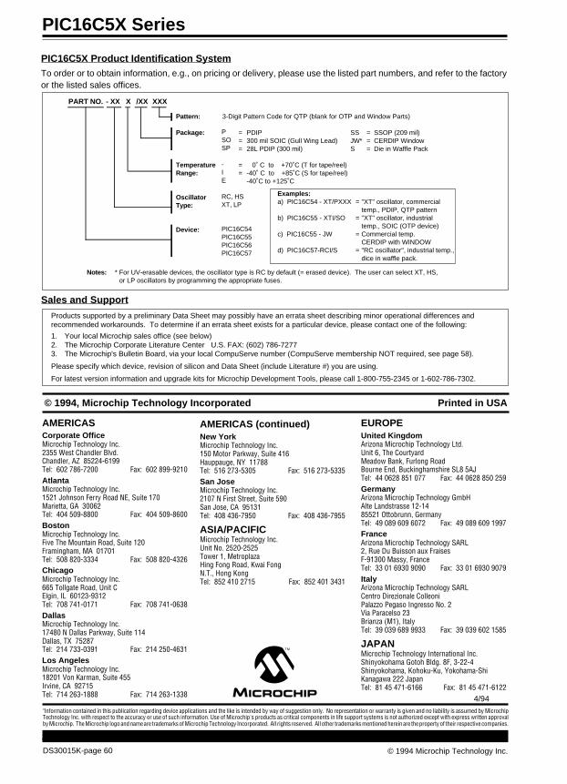
DS30015K-page 60
PIC16C5X Series
© 1994 Microchip Technology Inc.
"Information contained in this publication regarding device applications and the like is intended by way of suggestion only. No representation or warranty is given and no liability is assumed by MicrochipTechnology Inc. with respect to the accuracy or use of such information. Use of Microchip's products as critical components in life support systems is not authorized except with express written approvalby Microchip. The Microchip logo and name are trademarks of Microchip Technology Incorporated. All rights reserved. All other trademarks mentioned herein are the property of their respective companies.
AMERICASCorporate OfficeMicrochip Technology Inc.2355 West Chandler Blvd.Chandler, AZ 85224-6199Tel: 602 786-7200 Fax: 602 899-9210AtlantaMicrochip Technology Inc.1521 Johnson Ferry Road NE, Suite 170Marietta, GA 30062Tel: 404 509-8800 Fax: 404 509-8600BostonMicrochip Technology Inc.Five The Mountain Road, Suite 120Framingham, MA 01701Tel: 508 820-3334 Fax: 508 820-4326ChicagoMicrochip Technology Inc.665 Tollgate Road, Unit CElgin, IL 60123-9312Tel: 708 741-0171 Fax: 708 741-0638DallasMicrochip Technology Inc.17480 N Dallas Parkway, Suite 114Dallas, TX 75287Tel: 214 733-0391 Fax: 214 250-4631Los AngelesMicrochip Technology Inc.18201 Von Karman, Suite 455Irvine, CA 92715Tel: 714 263-1888 Fax: 714 263-1338 4/94
EUROPEUnited KingdomArizona Microchip Technology Ltd.Unit 6, The CourtyardMeadow Bank, Furlong RoadBourne End, Buckinghamshire SL8 5AJTel: 44 0628 851 077 Fax: 44 0628 850 259GermanyArizona Microchip Technology GmbHAlte Landstrasse 12-1485521 Ottobrunn, GermanyTel: 49 089 609 6072 Fax: 49 089 609 1997FranceArizona Microchip Technology SARL2, Rue Du Buisson aux FraisesF-91300 Massy, FranceTel: 33 01 6930 9090 Fax: 33 01 6930 9079ItalyArizona Microchip Technology SARLCentro Direzionale ColleoniPalazzo Pegaso Ingresso No. 2Via Paracelso 23Brianza (M1), ItalyTel: 39 039 689 9933 Fax: 39 039 602 1585
JAPANMicrochip Technology International Inc.Shinyokohama Gotoh Bldg. 8F, 3-22-4Shinyokohama, Kohoku-Ku, Yokohama-ShiKanagawa 222 JapanTel: 81 45 471-6166 Fax: 81 45 471-6122
AMERICAS (continued)New YorkMicrochip Technology Inc.150 Motor Parkway, Suite 416Hauppauge, NY 11788Tel: 516 273-5305 Fax: 516 273-5335San JoseMicrochip Technology Inc.2107 N First Street, Suite 590San Jose, CA 95131Tel: 408 436-7950 Fax: 408 436-7955
ASIA/PACIFICMicrochip Technology Inc.Unit No. 2520-2525Tower 1, MetroplazaHing Fong Road, Kwai FongN.T., Hong KongTel: 852 410 2715 Fax: 852 401 3431
PIC16C5X Product Identification SystemTo order or to obtain information, e.g., on pricing or delivery, please use the listed part numbers, and refer to the factoryor the listed sales offices.
PART NO.
PSOSP
-IE
RC, HSXT, LP
PIC16C54PIC16C55PIC16C56PIC16C57
3-Digit Pattern Code for QTP (blank for OTP and Window Parts)
- XX X /XX XXX
PDIP300 mil SOIC (Gull Wing Lead)28L PDIP (300 mil) 0˚C to +70˚C (T for tape/reel) -40˚C to +85˚C (S for tape/reel)-40˚C to +125˚C
Package:
TemperatureRange:
Oscillator Type:
Device:
===
==
For UV-erasable devices, the oscillator type is RC by default (= erased device). The user can select XT, HS, or LP oscillators by programming the appropriate fuses.
Notes:
Examples:a) PIC16C54 - XT/PXXX
b) PIC16C55 - XTI/SO
c) PIC16C55 - JW
d) PIC16C57-RCI/S
=
=
=
=
"XT" oscillator, commercial temp., PDIP, QTP pattern"XT" oscillator, industrial temp., SOIC (OTP device)Commercial temp. CERDIP with WINDOW"RC oscillator", industrial temp., dice in waffle pack.
Pattern:
SSJW*S
===
SSOP (209 mil)CERDIP WindowDie in Waffle Pack
*
Sales and Support
Products supported by a preliminary Data Sheet may possibly have an errata sheet describing minor operational differences andrecommended workarounds. To determine if an errata sheet exists for a particular device, please contact one of the following:
1. Your local Microchip sales office (see below)2. The Microchip Corporate Literature Center U.S. FAX: (602) 786-72773. The Microchip's Bulletin Board, via your local CompuServe number (CompuServe membership NOT required, see page 58).
Please specify which device, revision of silicon and Data Sheet (include Literature #) you are using.
For latest version information and upgrade kits for Microchip Development Tools, please call 1-800-755-2345 or 1-602-786-7302.
© 1994, Microchip Technology Incorporated Printed in USA