epsrc cdt ism projects (2015/16 entry) - glaarharvey/cdt-ism_projects.pdf · epsrc cdt-ism projects...
TRANSCRIPT

EPSRC CDT-ISM Projects (2015/16 Entry) We list below the titles and abstracts for projects being offered for entry in 2015/16. To apply for a PhD position, please submit a CV and covering letter to [email protected] Your covering letter should list the projects that are of most interest to you and highlight how your experience and interests are pertinent to these projects. Summary of Projects: Universities of Glasgow and Edinburgh See the following section for abstracts for each of the projects listed in this section. University of Glasgow G1: Computational imaging in fluorescence microscopy Dr Jonathan Taylor, School of Physics and Astronomy, University of Glasgow G2: Hybrid computational- optical techniques for microscopy and retinal imaging Professor Andrew Harvey, School of Physics and Astronomy, University of Glasgow G3: Integrated biosensors for field-based diagnostics Dr Julien Reboud, School of Engineering, University of Glasgow G4: New optical techniques for probing molecular chirality Professor Stephen M. Barnett, School of Physics and Astronomy, University of Glasgow G5: Quantitative optical imaging in the eye Professor Andrew Harvey, School of Physics and Astronomy, University of Glasgow G6: Quantum Enhanced Wavelength Transformation Imaging Professor Miles Padgett, School of Physics and Astronomy, University of Glasgow G7: Quantum Inspired Imaging Professor Miles Padgett, School of Physics and Astronomy, University of Glasgow G8: Sensing, Control and Selection of and Growth of Chiral Inorganic Materials Professor Lee Cronin, School of Chemistry, University of Glasgow G9: The Multicorder: CMOS sensor technology for chemical synthesis Professor David Cumming, School of Engineering, University of Glasgow G10: The Multicorder: CMOS sensor technology for the metabolome Professor David Cumming, School of Engineering, University of Glasgow G11: The Multicorder: Nanophotonics for integrated sensing and imaging

Professor David Cumming, School of Engineering, University of Glasgow G12: The Sonopill: CMOS sensor technology Professor David Cumming, School of Engineering, University of Glasgow G13: STED inspired sensors for tomographic imaging of darkness Dr Sonja Franke-Arnold, School of Physics and Astronomy, University of Glasgow G14: A new metamatieral sensor for sub-femtomole stereochemical detection Dr Malcom Kadodwala, School of Chemistry, University of Glasgow
G15: Interferometric Sensors With Back Action Noise Evasion Dr. Stefan Hild, School of Physics and Astronomy, University of Glasgow
G16: Seebeck Microscopy Professor John Weaver, School of Engineering, University of Glasgow
G17: Advanced Antenna Sensors for Optical Nanomeasurement Professor John Weaver, School of Engineering, University of Glasgow University of Edinburgh E1: Photonic crystal fibres for chemical sensing and photochemistry Prof Anita Jones, School of Chemistry, University of Edinburgh E2: Innovation in Electrochemical Sensor development utilizing Inkjet/Printing Drop on Demand (DoD) technology Dr Dimitrios Kampouris, School of Chemistry, University of Edinburgh E3: Implanted Optical Sensors for pH and Hypoxia Prof Alan Murray, School of Engineering, University of Edinburgh E4: Wireless Power and Communications for Implanted Sensor Devices Prof Alan Murray, School of Engineering, University of Edinburgh E5: Bioelectronic methods for sensors based on engineered bacterial growth responses Dr. Stewart Smith, School of Engineering, University of Edinburgh E6: Contact lens-based Sensing Prof Ian Underwood, School of Engineering, University of Edinburgh E7: Smart 2D Ultrasonic Transducer Array Prof Ian Underwood, School of Engineering, University of Edinburgh E8. Characterisation of magnetic films for integrated micro-components and sensors First supervisor: Prof Anthony Walton

E9. Development and Characterisation of Nano Electrode Arrays for Electrochemical Sensing First supervisor: Prof Anthony Walton E10. Development of Microelectrode Sensor Systems for Operation in Harsh Environments (funded positions available) First supervisor: Prof Anthony Walton E11. Development of temperature and pressure sensing technology to characterise and monitor the performance of microchannels using the boiling of liquids to cool microelectronic devices (funded positions available) First supervisor: Prof Anthony Walton
Eligibility requirements You must have a good first degree (2:1 or above) in an appropriate Physical Sciences or Engineering discipline. Applicants with a degree in Chemistry should have an interest and aptitude for sensing and measurement. Some that projects specify more specialist requirements.

Projects at The University of Glasgow G1: Computational imaging in fluorescence microscopy First Supervisor: Dr Jonathan Taylor Second Supervisor: Professor Andy Harvey This project will combine computational imaging and compressive sensing techniques with SPIM microscopy, with the aim of increasing the speed, quality and field of view of imaging inside living tissue. The focus will be on the development of new imaging and sensing techniques for fluorescence microscopy, with the ultimate aim of improving microscope imaging capabilities for biologists studying living animals such as the zebrafish. The ideally suited student will have a strong interest in designing and building new optical imaging systems, along with the mathematical and computational skills necessary to recover a high quality 3D image from the measurements.
3D image of a beating zebra-fish heart G2: Hybrid computational-optical techniques for microscopy and retinal imaging First Supervisor: Professor Andrew Harvey Second Supervisor: Dr Jonathon Taylor The student will work in the exciting and fast-moving field of computational optical imaging, combining optics and imaging science with computational techniques for recovering images. S/he will devise new optical techniques for recording image information in the presence of high levels of aberrations or clutter introduced by the optics or by the sample to be imaged and will develop algorithms for recovery of three-dimensional images from this information. The new techniques will then be adapted for application in microscopy (for example, fluorescence and two-photon microscopy) for life-science applications for in vitro, ex vivo and in vivo imaging. It is expected that the student will also apply computational imaging to enable enhanced imaging of the retina.
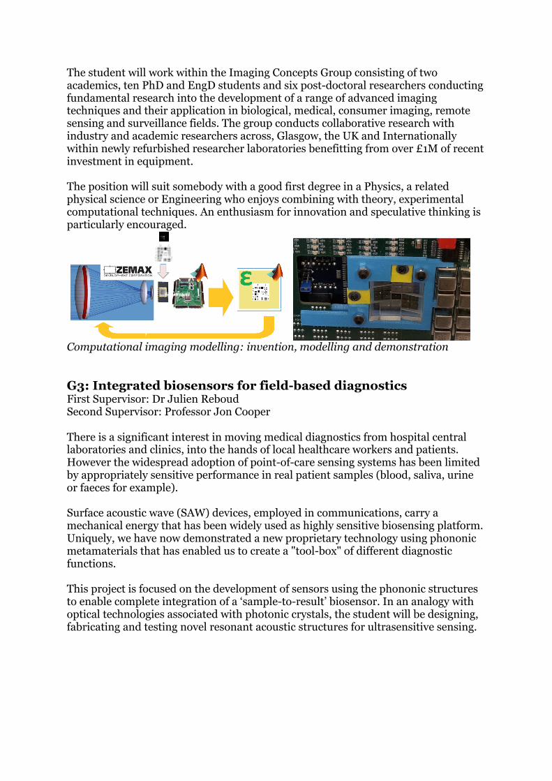
The student will work within the Imaging Concepts Group consisting of two academics, ten PhD and EngD students and six post-doctoral researchers conducting fundamental research into the development of a range of advanced imaging techniques and their application in biological, medical, consumer imaging, remote sensing and surveillance fields. The group conducts collaborative research with industry and academic researchers across, Glasgow, the UK and Internationally within newly refurbished researcher laboratories benefitting from over £1M of recent investment in equipment. The position will suit somebody with a good first degree in a Physics, a related physical science or Engineering who enjoys combining with theory, experimental computational techniques. An enthusiasm for innovation and speculative thinking is particularly encouraged.
Computational imaging modelling: invention, modelling and demonstration G3: Integrated biosensors for field-based diagnostics First Supervisor: Dr Julien Reboud Second Supervisor: Professor Jon Cooper There is a significant interest in moving medical diagnostics from hospital central laboratories and clinics, into the hands of local healthcare workers and patients. However the widespread adoption of point-of-care sensing systems has been limited by appropriately sensitive performance in real patient samples (blood, saliva, urine or faeces for example). Surface acoustic wave (SAW) devices, employed in communications, carry a mechanical energy that has been widely used as highly sensitive biosensing platform. Uniquely, we have now demonstrated a new proprietary technology using phononic metamaterials that has enabled us to create a "tool-box" of different diagnostic functions. This project is focused on the development of sensors using the phononic structures to enable complete integration of a ‘sample-to-result’ biosensor. In an analogy with optical technologies associated with photonic crystals, the student will be designing, fabricating and testing novel resonant acoustic structures for ultrasensitive sensing.
G4: New optical techniques for probing molecular chirality First Supervisor: Professor Stephen M. Barnett Second Supervisor: Dr Robert P. Cameron Many molecules possess forms that distinguish them from their mirror images, much like a human hand. These handed, or chiral, molecules are of great importance, owing in particular to the vital role played by molecular chirality in biological function. Sensing chiral molecules and measuring their properties nevertheless remains a challenging task, owing primarily to the smallness of the signals involved. It can also be argued that there stands much more to be learnt about molecular chirality than is offered by the currently adopted techniques. The aim of the project is to tackle these issues by identifying and developing, in theory, new techniques for sensing chiral molecules and measuring their properties. G5: Quantitative optical imaging in the eye First Supervisor: Professor Andrew Harvey Second Supervisor: Dr Jonathon Taylor The Imaging Concepts Group pioneers new techniques for quantitative imaging within the eye including multispectral imaging of retinal and scleral blood oxygenation, computational scanning laser ophthalmoscopy, optical coherence tomography and imaging of retinopathy of prematurity. In this project the student will develop and apply new techniques for quantitative retinal imaging including using structured light and snapshot spectral imaging to quantify retinal chromophors, metabolism and to characterise systemic vasculature. That is, imaging of the retina will be used as a window on systemic health. The student will use and apply the principles of optics, imaging and mathematics at a deep level and will develop a working understanding of the relevant biology through specialist courses and through collaboration with clinicians and biologists. The student will work within the Imaging Concepts Group consisting of two academics, ten PhD and EngD students and six post-doctoral researchers conducting fundamental research into the development of a range of advanced imaging techniques and their application in biological, medical, consumer imaging, remote sensing and surveillance fields. The group conducts collaborative research with industry and academic researchers across, Glasgow, the UK and Internationally within newly refurbished researcher laboratories benefitting from over £1M of recent investment in equipment. The position will suit somebody with a good first degree in Physics, a related physical science or Engineering who enjoys combining with theory, experimental and computational techniques and is attracted to research at the life-science interface. An enthusiasm for innovation and speculative thinking is particularly encouraged.
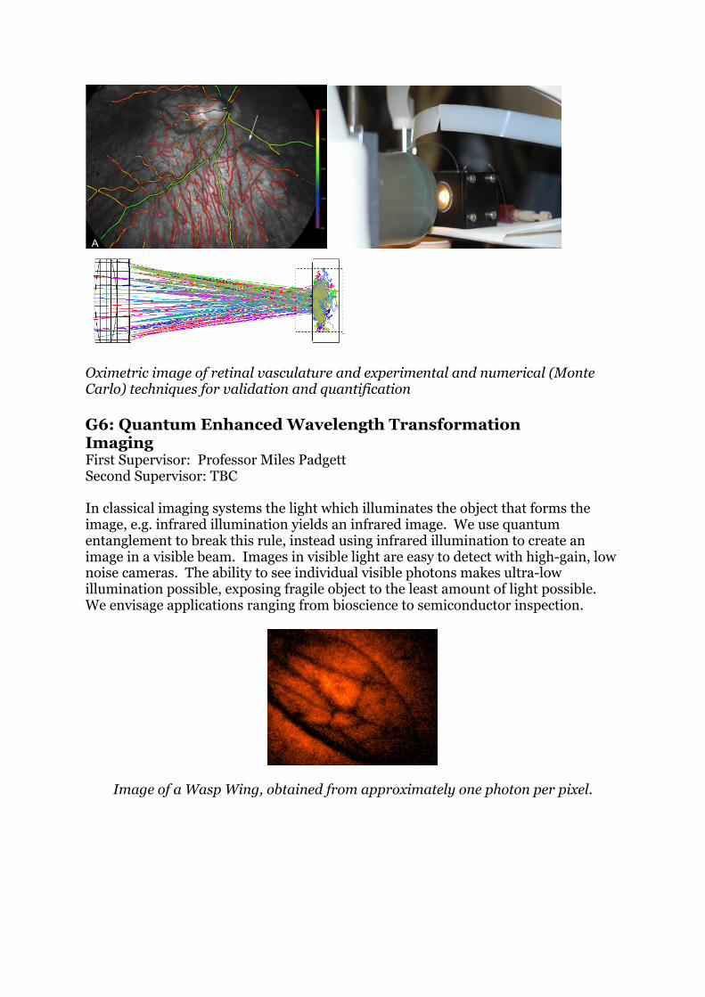
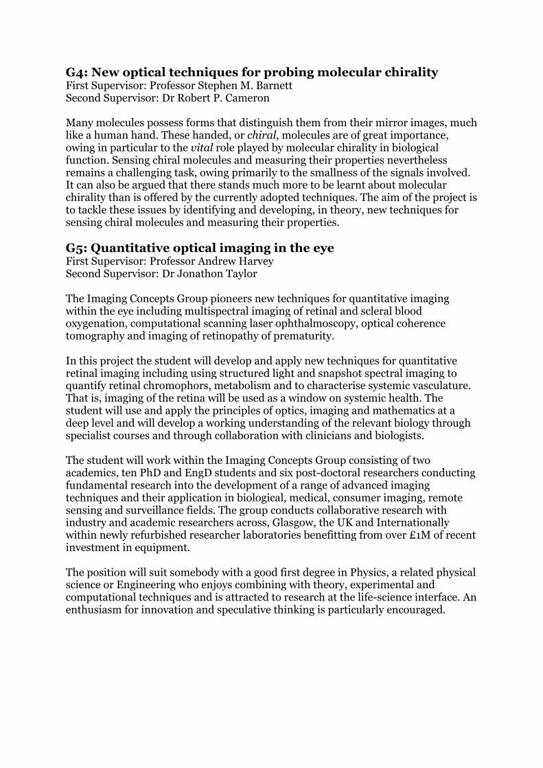
Oximetric image of retinal vasculature and experimental and numerical (Monte Carlo) techniques for validation and quantification G6: Quantum Enhanced Wavelength Transformation Imaging First Supervisor: Professor Miles Padgett Second Supervisor: TBC In classical imaging systems the light which illuminates the object that forms the image, e.g. infrared illumination yields an infrared image. We use quantum entanglement to break this rule, instead using infrared illumination to create an image in a visible beam. Images in visible light are easy to detect with high-gain, low noise cameras. The ability to see individual visible photons makes ultra-low illumination possible, exposing fragile object to the least amount of light possible. We envisage applications ranging from bioscience to semiconductor inspection.
Image of a Wasp Wing, obtained from approximately one photon per pixel.

G7: Quantum Inspired Imaging First Supervisor: Professor Miles Padgett Second Supervisor: TBC Digital cameras are often sold on the basis of the number of pixels they have. At the University of Glasgow we design cameras, not with many millions of pixels but just one. Use of a single pixel means that low-cost camera can be designed to cover any wavelength from the UV to the infra-red. Application areas range from the detection of gas leaks to the enhancement of imaging through smoke and haze
G8: Sensing, Control and Selection of and Growth of Chiral Inorganic Materials First Supervisor: Professor Lee Cronin Second Supervisor: Professor Miles Padgett Chemical Robotics for materials growth and assembly by optical control. In this project we will design, build and utilise a chemical-robotic system for the observation, selection, and directed assembly of chiral inorganic materials. With feedback control we will use chiral spectroscopy to directly selected materials of the desired chirality, see Figure.
Figure. LEFT: Schematic of one of our previous set ups used for optical control of materials. RIGHT: example off the directed growth of an ‘inorganic star’ made from an inorganic tube. The red circle shows the position of the laser spot and the path that the control system directed the laser to take to draw the star is shown.
G9: The Multicorder: CMOS sensor technology for chemical synthesis First Supervisor: Professor David Cumming Second Supervisor: Professor Lee Cronin Microelectronics technology has led to a revolution in computer and communication technology that began almost immediately that the transistor was invented. The exponential rate of technological advancement that is described in Moore’s Law has been propelled by $1Tr of investment over 50 years. However, CMOS technology, which now dominates the microelectronics industry, has proven itself to be immensely versatile. For example, the digital camera chip that uses silicon photodiodes (PD) is now ubiquitous. More recently CMOS has been exploited to make the large arrays of ion sensitive field effect transistors (ISFET) used in the Ion Torrent and Ion Proton Next Generation sequencing systems. Exciting new opportunities now lie in pursuing non-roadmap “More than Moore” technology to discover and exploit the as yet unfulfilled potential of CMOS in markets and applications that have historically lain outside the realm of microelectronics. We will explore our capability in the use of CMOS integrated sensor arrays, such as the “proton camera” with the objective of real-time, direct observation of ionic behaviour in chemical reaction dynamics. This work will entail improvement to existing systems as well as preparation and demonstration of the proposed optically based sensor arrays in this application. The Cronin group has pioneered novel synthesis techniques that include 3D printing and multichannel flow and microfluidic reactors for the investigation of complex chemical systems and rapid synthesis of complex molecular products. A speculative objective of the programme will be the possibility of measuring and then producing target therapeutic chemistries in response to measurement and analysis of patient samples. Eligibility requirements To undertake this research, we are seeking a motivated candidate with a good first degree in Chemistry, Electronic and Electrical Engineering, or a cognate discipline. Some knowledge and experience of sensors, experimental work in a chemical context and instrumentation/date acquisition would be an advantage. G10: The Multicorder: CMOS sensor technology for the metabolome First Supervisor: Professor David Cumming Second Supervisor: Professor Mike Barrett Microelectronics technology has led to a revolution in computer and communication technology that began almost immediately that the transistor was invented. The exponential rate of technological advancement that is described in Moore’s Law has been propelled by $1Tr of investment over 50 years. However, CMOS technology, which now dominates the microelectronics industry, has proven itself to be immensely versatile. For example, the digital camera chip that uses silicon photodiodes (PD) is now ubiquitous. More recently CMOS has been exploited to make the large arrays of ion sensitive field effect transistors (ISFET) used in the Ion Torrent and Ion Proton Next Generation sequencing systems. Exciting new

opportunities now lie in pursuing non-roadmap “More than Moore” technology to discover and exploit the as yet unfulfilled potential of CMOS in markets and applications that have historically lain outside the realm of microelectronics. The Multi-Corder chip must have very broad sensor modalities, from fundamental metabolite detection and quantification, through ligand-binding-based detection thence on to whole organism detection. The sensors we propose to deliver this range of functionality are not purely CMOS, but require both small and large surface features, on the scale of MEMS technology, to interact effectively with the different measurands. Achieving the objective of multi-modality on a single chip will be a major technological challenge in both engineering and biology. Using CMOS we will design and fabricate a range of detectors that must be functionalised in order to create sensors. We will do this by lithographically surface patterning the CMOS chip surface that we will have prepared with suitable immobilisation chemistries. We will select chemical moieties and use these to prepare new materials, as well as investigating commercially available products. Eligibility requirements To undertake this research, we are seeking a motivated candidate with a good first degree in Electronic and Electrical Engineering, Biomedical Engineering, or a cognate discipline. Some knowledge and experience of VLSI technology, sensors, experimental work and an ability to work effectively with researchers in biology will be necessary. Exceptionally, we will consider a candidate with a background in biochemistry. G11: The Multicorder: Nanophotonics for integrated sensing and imaging First Supervisor: Professor David Cumming Second Supervisor: TBC An opportunity is available to an excellent student to work on nanophotonic physics and engineering to realise a sophisticated biomedical diagnostic system. The resulting technology will also have applications in new imaging technologies, including quantum enhanced imaging for medical and security applications. As a research student you will be given the opportunity to work on design and fabrication of novel surface plasmon resonance or metamaterial based structures for photonic signal enhancement. You will work on chemical functionalization, supported by collaboration with leading chemists and biochemists in the University of Glasgow. You will also receive full training and the freedom to use the University’s excellent James Watt Nanofabrication Centre where we have state-of-the-art electron beam lithography and associated technologies that underpin our position as world leaders. You will be a member of the Microsystem Technology group that presently has 9 post-doctoral research fellows, all of whom are active in supporting research student training and development. You will join a group of peers and share ideas and develop new research ideas as a valued member of a team.

Eligibility requirements To undertake this research, we are seeking a motivate candidate with a good first degree in Physics, Electronic and Electrical Engineering, or a cognate discipline. Some knowledge and experience of sensors, experimental work in electronics, physics or chemistry, and instrumentation/data acquisition would be an advantage. G12: The Sonopill: CMOS sensor technology First Supervisor: Professor David Cumming Second Supervisor: TBC Our vision is of a capsule that can be swallowed comfortably, incorporating diagnostic and therapeutic ultrasound along with optical imaging. This will be complemented by other sensors, e.g. for pH measurement and autofluorescence imaging (AFI) for multimodal diagnosis. The capsule will allow autonomous positioning and will have multiple deployment modes: from an endoscope or swallowed directly, and tethered or with full autonomy. When a patient presents with a GI complaint, the use of such a capsule will be an early diagnostic choice rather than the current relatively late choice of conventional endoscopy (Fleischer, 2010). It may be deployed by a general practitioner, nursing staff, or a consultant. The capsule will provide information on the condition of the GI tract, both superficially and beneath the surface, and the same device or a different one will allow localised treatment, e.g. of cancer, haemorrhage or IBD. In the longer term, we foresee for GI conditions a family of diagnostic and therapeutic capsules no larger than paracetamol caplets, with the patient pathway defined according to diagnostic information assembled as different modalities, visual, ultrasonic, chemical and photonic, are utilised. A student is required to focus effort on CMOS based sensor design and integration into the capasule format to work alongside the acoustic technology that is being developed by colleagues in Dundee University. The student will be required to become adept at design, test and characterization of unpackaged and packaged device, possibly with an opportunity to work alongside surgeons. Eligibility requirements To undertake this research, we are seeking a motivated candidate with a good first degree in Electronic Engineering, or a cognate discipline. Some knowledge and experience of VLSI, sensors, experimental work and instrumentation/data acquisition would be an advantage. G13: STED inspired sensors for tomographic imaging of darkness First Supervisor: Dr Sonja Franke-Arnold Second Supervisor: Dr Johnathan Taylor This project will develop a 3D sensor for structures of darkness. You will build a prototype tomography system based on scattering of near-resonant light from an atomic rubidium vapour and 3D fluorescence detection. The mechanism relies on the competition between a strong structured light beam which comprises braided or knotted vortex lines, and a weak probe laser with a flat amplitude and phase profile. In analogy with STED microscopy, we expect to achieve high resolution 3D imaging of the complete vortex topology. The project aims to demonstrate 3D spatial filtering for super-resolution sensing of biological samples.

G14: A new metamatieral sensor for sub-femtomole stereochemical detection First Supervisor: Dr Malcom Kadodwala Second Supervisor: Dr Donald Maclaren Drug molecules, both therapeutic and illicit, typically possess a sense of handedness, a property known as chirality. They are conventionally detected and their purity checked using polarimetry techniques that are sensitive to milligram levels. We have recently discovered a new detection method, using chirally-nanostructured oxides, that will improve the chiral sensitivity down to the picogram (million millionth of a gram) level. This project will exploit our discovery to develop a new instrument that is suitable for point of care medical diagnostics and the detection of illegal drugs. The project will be conducted as part of a major new UK-Japan collaboration. G15: Interferometric Sensors With Back Action Noise Evasion First Supervisor: Dr. Stefan Hild Second Supervisor: Prof. Kenneth Strain This project aims at laying the foundation for long-term improvements of sensors and measurement devices beyond the quantum limit. It seems very likely that the rapid progress of miniaturising of sensors and vastly increasing their application range that we have all witnessed in our day-to-day life over the past decade will continue in future. With smaller and smaller sensor systems, featuring at the same time increased sensitivity, it is not hard to image that in the mid-term future we will be limited by readout noise and back-action noise of our optical sensors. This project will develop new optical readout strategies for readout systems evading back-action noise using so-called quantum non-demolition techniques, such speedmeters or the application of squeezed light states.
Figure 1: Preliminary measurements of 3D vortex tomography. a) Atomic transitions, with structured light beam at 795nm and weak reference beam at 780nm. Tomographic measurements of the bright structure (b) and the dark areas detected at 780nm (c).

G16: Seebeck Microscopy First Supervisor: Prof. John Weaver, Second Supervisor: Dr. Phil Dobson, Advanced nanostructuring offers exciting new possibilities in the development of thermoelectric materials for energy harvesting. However, the characterisation of materials on such a small scale presents many challenges. To quickly evaluate these new materials we would like to measurement their Seebeck coefficient at the nanoscale. The Seebeck effect is the conversion of a temperature gradient into an electrical potential gradient, a key property of thermoelectric materials which is exhibited by all electrical conductors. The Seebeck effect also provides a window into the bandstructure of nanomaterials and nanostructures which is not readily available by any other means. Work pioneered at the University of Glasgow offers the possibility of measuring the Seebeck coefficient at the smallest scales by employing Atomic Force Microscopy (AFM) probes with integrated nano-sensors. The successful realisation of these devices will have a significant impact on the way new candidate thermoelectric materials are developed and evaluated. During the project we will develop advanced sensors for the simultaneous imposition of a known temperature gradient on a material and measurement of the resulting potential difference. This will involve the fabrication of advanced thermal-electrical nanosensors, the development of suitable instrumentation for their application and the measurement of a number of significant nanomaterials and structures. The work will take place in the AFM group in the School of Engineering which consists of two academic staff members, two RAs and four PhD students. The work will involve a broad range of work in nanofabrication, instrumentation, modelling and materials science and would suit a good graduate in Electronic Engineering or Physical Sciences.
A Scanning Thermal Microscope probe fabricated at Glasgow: This consists of a platinum thermometer sensor on the end of a conventional atomic force microscope sensor probe.

G17: Advanced Antenna Sensors for Optical Nanomeasurement First Supervisor: Prof. John Weaver, Second Supervisor: Dr. Phil Dobson, Optical measurements allow the measurement of a vast range of important physical and chemical properties of materials at the micro-scale. Far-field optical measurements are limited to a resolution of about half a wavelength of light which limits their utility in characterising nanostructures. In addition, optical microanalysis is often limited by the signals available from a small volume of material. Metals have a very large (imaginary) refractive index at optical frequencies. As a consequence, the confinement of optical fields by a metal can result in a large increase in the available spatial resolution of an optical sensing system whilst still allowing the use of normal spectroscopic sensing. By structuring the metal at the nanoscale one can also use plasmonic effects to cause the optical electric fields to be locally magnified by several orders of magnitude. This potentially enables spectroscopy of single molecules to be performed, or the coupling of an optical sensor to evanescent fields, such as thermally excited surface plasmon polaritons. This project is concerned with the development of advanced sensors in which an optimised plasmonic antenna is coupled to a lithographically-defined field concentrator at the end of an atomic force microscope tip. The sensor will be applied to the reliable achievement of a vast increase in the efficiency of Tip Enhanced Raman Spectroscopy and, speculatively, in the study of near-field black body radiative transport. The work will take place in the AFM group in the School of Engineering which consists of two academic staff members, two RAs and four PhD students. The work will involve a broad range of work in nanofabrication, optics, modelling and scanned probe microscopy and would suit a good graduate in Electronic Engineering or Physical Sciences.
An aperture in a thick aluminium film allowing sub-wavelength control of near-field optical intensity on the basis of polarisation.
200nm

Projects at the University of Edinburgh E1. Photonic crystal fibres for chemical sensing and photochemistry First supervisor: Prof Anita Jones Second supervisor: Dr Jochen Arlt The aim of this project is to exploit the unique optofluidic properties of photonic crystal fibre for applications in chemical sensing and photochemistry. A primary objective will be the development of a PCF-based system for evaluating the performance of photo-activated drugs in response to two-photon excitation, in the context of photodynamic cancer therapy. Further Information: Photonic crystal fibre (PCF) is a novel optofluidic system in which light and chemical samples can strongly interact, over extended path-lengths, for quantitative, ultrasensitive spectroscopic analysis or photo-activation. In PCF, light is trapped in the hollow core of the optical fibre by the surrounding 2D periodic ‘photonic crystal’ cladding. This permits the infiltration of a sample of gas or liquid into the hollow core, while maintaining the high optical transmission efficiency of the fibre. This project will build on our pioneering studies on intra-fibre excitation of solution-phase samples, which have started to reveal the potential of PCF for chemical sensing and photochemical applications. A PCF-based optofluidic platform will be developed to measure the performance of newly developed, two-photon-activated anticancer agents by ultrasensitive luminescence detection of singlet oxygen production. This will exploit our recent discovery that two-photon excitation can be sustained over exceptional path-lengths in PCF. E2. Innovative Electrochemical Sensor Development Utilising Inkjet/Printing Drop on Demand (DoD) Technology First supervisor: Dr Dimitrios Kampouris Second supervisors: Professor Andy Mount, Dr Jon Terry Low printing speeds and issues on the printing quality, according to criteria set by the Electronic industry, limit the wide use of IJP as a manufacturing tool. The project explores possible pathways which could overcome these challenges and studies these pathways on the electrochemical sensor development by IJP technique. Further Information: The aim of the project is the development of electrochemical sensors, utilizing the inkjet printed technology (Drop on Demand DoD), on various substrates (polymer, paper silicon, arbitrary). The project will focus on the development of 3 electrode sensors (working, reference and counter electrode), with the end goal being a multi (working) electrode array sensor , utilizing IJP technology, for the simultaneous monitoring of various analytes, through the functionalization of different working electrodes on the multi electrode array. Inkjet printing (IJP) technology is a very promising tool for the manufacturing industry. Electronic industry utilizes IJP for the manufacturing of LED’s and

exploits the applicability of the technique for the manufacturing of printed/plastic electronics, photovoltaic cells for power generation, sensors etc. The IJP technique is quite competitive with the conventional printing techniques due to its versatility (no need for masks or screen patterns) and its accurate and reproducible delivery of the ink under digital control. It is also quite important that it is a non-contact printing method, which is quite useful for the electronic industry and there is a minimum waste of ink. The main limit the technique face, is the low volume of printing. The problem lies to the low printing speeds and the lower, to the industry set standards, printing quality criteria. All these problems preventing the IJP technique from dominating the area of manufacturing in electronic industry can lie to three main limits:
1. While lots of research has been conducted on the delivery of the drop size and shape, it seems that more and more increasingly important is the landing and spreading behaviour of the droplet on the substrate and especially of the dissolved material (pigment) in the droplet and the pattern it creates on the substrate.
2. There are certain constraints of the ink formulation used for IJP. One of the limits for the IJP technology is the slow delivery of the printing material which lies on the low concentration of the pigment (dissolved material) in the ink used. The low pigment concentration in the ink formulation and the slow drying solvents used in IJP (to prevent clogging of the nozzles) allows some non-linear processes to occur at the drop once landed on the substrate such as the Marangoni-effect (coffee ring stain) which gives rise to an uneven distribution of the final material (the dissolved material gathers at the edges of the drop). This is a significant problem for the electronic industry (and especially for the sensor development) since the current flows through the edges of the pattern decreasing significantly its conductivity and in combination with gaps in the pattern, it transforms IJP technology of no functional use for the electronic industry.
3. Only few ink formulations have been developed with good resistivity values of the tracks printed. Ag (nanoparticles or precursors) ink formulations are the only inks produced with high content of pigment (>10%w/w), they have reached 60%w/w levels, and a resistivity of the printed tracks reaching few µΩΩcm after depositing more than 10 layers of the ink (10 passes). Other inks used for sensing applications (or generally within the electronic industry) is graphene (including composites of graphene) with pigment content 2%w/v, and resistivity values of the printed tracks of few mΩΩcm after depositing more than 10 layers of the ink (10 passes). Polythiophene (2%w/v pigment content) ink formulations have reached resistivity values within the region of 500ΩΩcm. Limits on the type of the pigment materials and their concentration in the ink formulation limits the application of IJP on sensor development.
The project will study three themes focused on key aspects of the sensor development utilizing the IJP technology: The formulation of various electrode materials and their impact on the rheology and jetting behaviour of the printing fluid; controlling the spreading behaviour of the drop delivered through IJP on various substrates and explore post-impact processes (thermal annealing, chemistry treatment etc) that determine the structure and functionality of the printed patterns; exploring the effect of the design of the multimicroelectrode arrays (MMEA), utilized by the IJP

technique (pattern prototyping digital controlled), on the electroanalytical performance of the arrays. E3. Implanted BioSensors for pH and Hypoxia First supervisor: Prof Alan Murray Second supervisors: Dr Stewart Smith and Prof Ian Underwood This project aims to develop support electronics and an integration platform for novel biosensors developed in Edinburgh (School of Chemistry). The sensors are ground-breaking examples of new ways to “interrogate” biology and the work will therefore be at the cutting edge of sensor technology. The student involved will:-
• Build an understanding of the principles and practice in a new biosensor form • Work with chemists to develop an integration strategy for these unique
sensors. • Construct and fabricate elements of the integration platform, working in
collaboration with the team on the IMPACT (Implanted Microsystems for Personalised Cancer Care) project
Further Information: Cancer kills over a million per annum in Europe alone. A malignant tumour is an uncontrolled growth of cells that can spread (metastasise) to distant organs. The microenvironment of a tumour is key to this spread and to the tumour’s resistance to radiotherapy. Implanted biosensors will allow a tumour’s biology to be monitored continuously and without further intervention. This project will develop novel in vivo biosensors of hypoxia and other key parameters of cancer biology. Subject to preclinical “proof in principle”, these biological data will be exploited therapeutically in treating cancers with RT in veterinary animal models. This project aims to explore the use of pH-sensitive polymers developed by the Bradley group in the School of Chemistry, Edinburgh, in combination with CMOS photodiode/SPAD sensors. These sensors require support electronics and possible post-processing fabrication techniques. Initially, the project will explore and evaluate the performance and support needs of a range of biosensors, selecting a target type at the end of year#2 of the CDT programme. Years 3-4 will be spent designing, fabricating and testing the necessary integration platform (on CMOS) for the chosen sensor type. Testing will be performed in vitro and in vivo via
collaboration with the School of Veterinary medicine. Biosensors in radiation treatment for cancer. A - a group of cancer cells B - radioresistant (1) and radiosensitive (2) cells with immune (3) and vascular (4) cells in the tumour microenvironment C - stereotactic insertion of biosensors into the microenvironment D - signal output (5) from biosensors in radioresistant zones E - differential deposition of radiation treatment to radioresistant zones. (adapted from Supiot et al, A. Cancer Radiother. 14(6-7):554-62. 2010).

E4. Wireless Power and Communications for Implanted Sensor Devices First supervisor: Prof Alan Murray Second supervisor: Dr Brian Flynn, Dr Martin Reekie This project will:
• Explore methods for wireless coupling in implanted sensors • Test the theoretical predictions in an existing model of coil-
coil communications • Develop an optimised strategy and set of circuits for communications between
an embedded sensor chip and a transceiver outside (perhaps worn on ) the body.
Cancer kills over a million per annum in Europe alone. A malignant tumour is an uncontrolled growth of cells that can spread (metastasise) to distant organs. The microenvironment of a tumour is key to this spread and to the tumour’s resistance to radiotherapy. Implanted biosensors will allow a tumour’s biology to be monitored continuously and without further intervention. This project will develop techniques for wireless communications between the implanted sensor and the medical team outside, to avoid infection that could be caused by wires that puncture the skin. The solution will be a combination of RF, inductive and ultrasonic communication. This project will explore novel fully-wireless and semi-wireless power supply and/or data communications for implanted sensor devices. We have already developed models of coil-coil coupling and this project will first assimilate and test them against experimental reality. Subsequently, the project will select the optimal combination of radio-frequency, inductive and ultrasonic communications to serve a sensor implanted in the human body, exchanging information with a transceiver outside the body. The project has opportunities for work in theoretical electromagnetic communications, experimental work on realistic test platforms and energy harvesting in implanted devices. The main thrust of the project will be defined during year#2 of the CDT programme and put into practice in years 3-4.

E5. Bioelectronic methods for sensors based on engineered bacterial growth responses First supervisor: Dr Stewart Smith Second supervisors: Prof Alistair Elfick, Dr Christopher French (School of Biological Sciences) Whole cell biosensors are living cells, usually bacteria, which have been genetically modified to produce a detectable response to a specific analyte. The response is most commonly luminescence or fluorescence, and with the GM nature of the organisms, this largely restricts such systems to laboratory use. For field use it would be advantageous to use non-transgenic organisms and cheap, rapid electrical/electronic detection systems. We propose a novel class of systems in which bacteria are engineered, without transgenesis, to respond to specific analytes by growing only in their presence. This will be combined with electrochemical transduction for sensitive detection of this growth, which can occur on a rapid time scale. Such systems may be suitable for point-of-care diagnostics as well as detection of environmentally significant analytes in the field. This is a multidisciplinary project involving both biological aspects (genetic modification) and engineering (fabrication of test devices). It is of considerable potential interest in biomedical, environmental and other sectors, and could also potentially be modified for rapid detection of pathogens, including antibiotic resistant bacteria. It will take advantage of the resources of the School of Engineering for the design and fabrication of microfluidic devices, micro/nano-electrodes and integrated systems. The combination of this capability with the expertise in the development of bacterial biosensing systems in the School of Biological Sciences represents a great opportunity for multidisciplinary collaboration.

E6: Contact lens-based Sensing First Supervisor: Prof Ian Underwood, School of Engineering Second Supervisor: Prof Bal Dhillon, College of Medicine and Vet Medicine This project aims to explore one or more sensor modalities and support functionalities that can be implemented in a contact lens platform. E7: Smart 2D Ultrasonic Transducer Array First Supervisor: Prof Ian Underwood, School of Engineering Second Supervisor: Prof Sandy Cochrane, University of Glasgow Third Supervisor: Dr Jon Terry, School of Engineering This project aims to demonstrate feasibility and produce prototype miniature 2D active matrix ultrasonic transducer array on CMOS for acoustic tweezing applications.
E8. Characterisation of magnetic films for integrated micro-components and sensors First supervisor: Prof Anthony Walton Second supervisor: Dr Jon This PhD project has the challenge of making it possible to fully integrate magnetic components (such as inductors) directly on top of silicon integrated circuits (More than Moore). It will involve the development fabrication of strain sensors and other test structures in conjunction advanced metrology tools to wafer mapping parameters such as composition (XRF), Young’s modulus (nanoindentation), resistivity, permeability and stress and these measurements will be used to first quantify the composition of the films and then investigate the mechanisms to minimise the stress levels resulting from different heat treatment regimes. Further Information: More than Moore technology (MtMT), which involves the integration of new materials and processes with standard integrated circuit (IC) technology, is becoming increasingly important. One of the key elements required for the successful MtMT integration of inductors, switches and sensors with ICs is the capability to deposit and characterise magnetic materials with the desired properties. In particular high permeability and low losses are key parameters as is the need to optimise the deposition process to also ensure low stress levels in the deposited films. This project will build upon extensive expertise at the SMC and will involve the further development of electrical and optical test structures to help optimise the process as well as wafer mapping the film composition and Young’s modulus. An example test structure is shown in figure 1.

Fig. 1. Strain test structure used to characterise the film strain in Permalloy (NiFe). Fig. 2 Simple micro-inductor / coil (Top), Coil Cross-section (Bottom) The project will be based in the SMC where there are world class facilities for both fabricating and characterising the technology on 200mm silicon wafers. These include two 200mm commercial electroplating machines and the ability to wafer map film composition using XRF, with a more recent addition being an automated nanoindenter that can rapidly wafer map Young’s modulus. Having fully characterised the materials and optimised the process and strain sensor structures the final element of the project will be exploit this knowledge to fabricate sensor coils and inductors compatible with CMOS IC technology. E9. Development and Characterisation of Nano Electrode Arrays for Electrochemical Sensing First supervisor: Prof Anthony Walton Second supervisor: Prof Andrew Mount This project is at the forefront of developments in nano electrode arrays, which have many attractive characteristics compared with micro and macro electrodes. It will involve developing and characterising of nanoelectrode arrays with different architectures using the state-of-the-art microfabrication tools available within the University of Edinburgh’s cleanroom facilities. The resulting sensor systems have applications in wide ranging areas which include healthcare and environmental monitoring. Unlike other methods of fabricating nanoelectrode, which employ sub-micron resolution photolithography described the Microsquare Nanoband Edge Electrode (MNEE) architecture is based upon micron level lithography, has reduced fabrication complexity and gives enhanced electroanalytical features, with independent array elements displaying steady-state response. It also has the added electroanalytical benefit that the electrical connection is not solely via the nanoband ends, which ensures there is negligible iR drop along the band length and makes the system insensitive to band breakage during fabrication and/or operation.

This novel architecture, with its low cost base provides many exciting opportunities and will be the starting point for this project, which will be at the forefront of developing and characterising multi-layer and multi-material architectures for a range of applications.
(a) Schematic diagram of the microsquare nanoband edge electrode (MNEE) array architecture, with Si3N4 and SiO2 insulation sandwiching a Pt nanoband in each square hole (inset), (b) An SEM image of a cleaved and polished cross section through a square hole in the fabricated structure. The thin Pt nanoband can be seen running horizontally leading to the etched area in the left of the picture; (c) An optical microscope image of the fabricated microsquare array. E10. Development of Microelectrode Sensor Systems for Operation in Harsh Environments (funded positions available) First supervisor: Prof Anthony Walton Second supervisor: Prof Andy Mount There are many applications that require the capability to operate within harsh environments. This includes the oil and gas industry (with temperatures down well-heads of over 200oC as well as in the nuclear industry for reprocessing spent fuels to deliver safe, reliable, economic and sustainable nuclear energy for both present and future reactor systems. In particular there is a pressing worldwide need to develop specific spent fuel reprocessing technology suitable for these reactors, as well as for dealing with legacy waste fuel from old reactors. Work to be undertaken This PhD project in Engineering and Chemistry offers challenging opportunities for a bright and motivated individual who can work both independently and as an integral part of a research team. The successful applicant will have responsibility for the development, fabrication and characterisation of electrochemical based micro and nano electrode based sensor systems to operate in harsh environment operationg at temperatures upto 550oC. The project will use state-of-the-art microfabrication tools available within the University of Edinburgh’s cleanroom facilities to fabricate sensor devices. These devices will then be characterised using our electrical and electrochemical test suites. The applicant should have an excellent undergraduate

degree in either Electrical Engineering, Chemistry or related discipline, and should have experience of practical laboratory work at undergraduate level.
Right, wafer with fabricated electrodes. Left, microelectrode design E11. Development of temperature and pressure sensing technology to characterise and monitor the performance of microchannels using the boiling of liquids to cool microelectronic devices (funded positions available) First supervisor: Prof Anthony Walton Second supervisor: Prof Khellil Sefiane This PhD project has the challenge of integrating temperature and pressure sensors in the bottom of cooling channels so that their performance can be characterised when using liquid boiling as device cooling mechanism. This project will for the first time provide engineers with the ability for simultaneous measurements/visualisation of bubble formation, and the temperature and pressure profile along a channel. Further Information: The background to the project is that advances in the manufacturing processes and the subsequent use of increased small-scale electronic devices operating at high power densities have brought about a dramatic demand for thermal management systems to provide extremely intensive localised cooling, and the estimated value associated with this thermal management industry is predicted to be $8.6 billion by 2015. Potential applications include electronic equipment, supercomputers, power devices, electric vehicles, photovoltaics, avionics and radar devices. The scientific and technical problems are also relevant to miniature fuel cells and gas-liquid reactors. In such systems, the effective heat transfer area is typically only a few cm2 and the cooling requirements range from heat fluxes of one to several MW/m2. Spatially

non-uniform and unsteady dissipative heat generation in such devices are detrimental to their performance and longevity. Liquid cooling systems, using complex channel designs, are only capable of achieving heat fluxes 0.7 MW/m2 and none of the other techniques (pool boiling, liquid jet impingement or sprays, curved channel or rotating stirrer cooling, heat pipes or capillary pumped loops, thermo-acoustic refrigeration and thermoelectric devices) have reached either a state of laboratory development or verification that they can deliver heat fluxes above 1 MW/m2. It is becoming clear that boiling in microchannels offers the best prospect for effectively meeting the needs of high heat flux devices and removing the heat transfer barriers currently limiting product developments. Heat sinks comprising many microchannels in parallel provide high ratio of coolant-to-thermal contact area. Additionally, flow boiling in microchannels enables much higher heat fluxes and greater uniformity of temperature. In a closed system an equally compact and effective condenser is needed for ultimate heat rejection to ambient air, or water in naval systems or by radiation in space applications. Microchannel condensers employing multichannel rectangular section tubes not only provide enhancement of the condensing side heat-transfer coefficient but enable very effective external finning arrangements. Therefore, flow boiling in microchannels, combined with condensation in a closed circulating system, offers a promising way of meeting the intensive cooling requirement for present and next-generation systems. However, significant difficulties remain to be overcome. At high heat flux, nucleate boiling gives way to film boiling in which the surface becomes blanketed by vapour vastly increasing the thermal resistance and leading to catastrophic rise in surface temperature (dry-out and critical heat flux (CHF)). Other difficulties relate to flow instabilities and flow reversal, which can reduce achievable heat transfer rates and increase pressure drop. This project will provide devices which will better characterise the performance of such systems, overcoming the problem of fabricating sensors in the bottom of cooling channels. Figures 1 to 3 show examples of devices designed and fabricated in the SMC cleanrooms. These devices have integrated sensors and heaters and the challenge in the PhD project is to add calibrated pressure sensors.

Right, wafer with three devices with 9 integrated heaters in their cooling channel. The heating element is fabricated on the back of the wafer. Left, device with an integrated heater and temperature sensors. The attached wires power up the heater.
Single channel device with integrated temperature sensors in its characterisation jig.