ergopro x365/565 quick reference guide - agrarixpub.agrarix.net/hw/fujitsu/ergopro...
TRANSCRIPT

PC Quick Reference Guide
ErgoProx365 & x565-series
Release 1

ErgoPro x365 and x565 series PC Quick Reference Guide
System board layout/jumper locations(AC41745 & AC41746)
JP13
JP10
JP1JP2JP3JP4
JP7
JP6
JP801VGA IRQenable/disable
Factory test
CPU Clock/Ratio
Audioenable/disable
FLASH BIOSupgrade enable/disable
CMOS Clear
JP14
PS/2 Mouse
Parallel portPS/2 Keyboard
Serial port 2
Serial port 1Line Out
Line In
Mic In USB RJ45 VGA
Page 2 Release 1
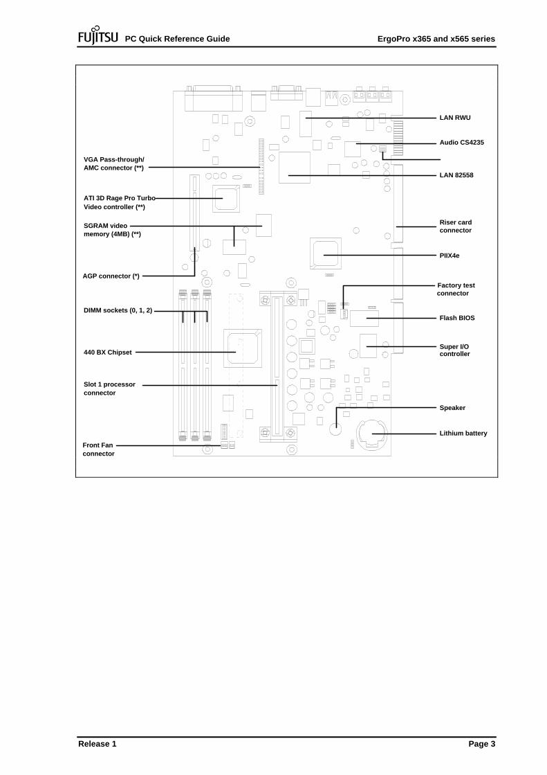
PC Quick Reference Guide ErgoPro x365 and x565 series
Flash BIOS
Lithium battery
PIIX4e
Slot 1 processor
ATI 3D Rage Pro Turbo
DIMM sockets (0, 1, 2)
Riser cardconnector
AMC connector (**)
Audio CS4235
LAN 82558
LAN RWU
Speaker
Super I/Ocontroller
connector
Video controller (**)
memory (4MB) (**)SGRAM video
VGA Pass-through/
440 BX Chipset
AGP connector (*)Factory testconnector
Front Fanconnector
Release 1 Page 3

ErgoPro x365 and x565 series PC Quick Reference Guide
System board jumpers (AC41745/746)
CPU Speed selection (JP1, JP2, JP3, JP4)To set the right CPU speed, set the jumpers as in the picture
JP1
JP2
JP3
JP4
350 MHz 400 MHz333 MHz300 MHz266 MHz
1
1
1
The speed of the Front Side Bus (FSB) is set automaticallyaccording to the CPU type.
450 MHz
111
1
CMOS CLEAR (JP6) and Factory test (JP7)To clear the CMOS, switch off the power and disconnect the mains cable. Take out the jumper from normaloperation position and install it in the clear CMOS position; keep it there for 10 seconds, then put the jumperback to normal operation position and reconnect the mains cable.
Normal
JP6
operationClearCMOS
Normal
JP7
operationFactory
testposition
Defaultsetting
Defaultsetting
Page 4 Release 1

PC Quick Reference Guide ErgoPro x365 and x565 series
Audio enable/disable (JP10)Jumper JP10 can be used to disable the on-board audio system.
Audio
JP10
enabledAudio
disabled
Default setting
Flash BIOS upgrade enable/disable (JP131 & JP141)VGA IRQ enable/disable JP801
JP13
JP801
EnabledDisabled
Defaultsetting
Flash BIOS upgrade disabled
Defaultsetting
Flash BIOS upgrade enabled
JP14
Defaultsetting
Flash BIOS BOOT block protected
Flash BIOS BOOT block
not protected
1
1
1 Depending on the system board version level, either one of the jumpers blocks JP13 or JP14 may not beinstalled
Release 1 Page 5

ErgoPro x365 and x565 series PC Quick Reference Guide
3-slot PCI/ISA back plane AC41748 ("front view")
PCI slot
System board connector
Modem WakeCD connector LAN Standby voltage connector
Floppy connector
Front board connector
Maintenance switchShared PC/ISA slots
Housing Fan connector
Fan (HDD) connector
HDD NTC
External HDD LED
Telephony connector
I2C-conv
Default (x365/***)
FP MIC EN
Default (x365/***)
Maintenance switchenable/disable
Default (x365/***)
3-slot PCI/ISA back plane AC41748 ("back view")
Primary IDE interface
Power supply connector
Supplemental power supply connectorSecondary IDE interface
Page 6 Release 1

PC Quick Reference Guide ErgoPro x365 and x565 series
5-slot PCI/ISA back plane AC41747 ("front view")
PCI slots
Modem WakeCD connector LAN Standby voltage connector
Floppy connector
Front board connector
Maintenance switchShared PC/ISA slot
Housing fan connector
Fan (HDD) connector
HDD NTC
External HDD LED
ISA slots
System board connector
Telephony connector
I2C-CONV
Default (x565/***)
Maintenance switchenable/disable
Default (x565/***)
FP MIC EN
Default (x565/***)
5-slot PCI/ISA back plane AC41747 ("back view")
Primary IDE interface
Power supply connector
Supplemental power supply connectorSecondary IDE interface
Release 1 Page 7
ErgoPro x365 and x565 series PC Quick Reference Guide
Processor related information
Processor related information
Used on x365/266 x365/300x564/300
x365/300x564/300
x365/333x564/333
Fujitsu code PL060621(active heatsink)
PL060630(passive heatsink)
PL060622(active heatsink)
PL060631(passive heatsink)
PL060623(active heatsink)
PL060627(passive heatsink)
Heatsink Active1 (with fan) and passive (no fan) heatsinks used.Heatsink attached to the processor’s SECC package
Processor & speed Intel Pentium II 266 MHz SECC
package300 MHz SECC package 333 MHz SECC
package
Technology 0.35 and 0.25 0.35 0.25 0.25
MMX support Yes
External clock(Front Side Bus)
66.7 MHz
Clock multiplier 4 4.5 5
System clock 33 MHz (PCI), 8.25 MHz (ISA)
Operating voltage PSU/regulator is automatically adjusted to the right voltage level by the VID pins ofthe processor
2.80 V (0.35technology)2.00 V (0.25technology)
2.80 V 2.00 V 2.00 V
Maximum powerconsumption of theprocessor chip (total)
38.2 W (0.35technology)
19.5 W (0.25technology)
43.0 W 21.7 W 23.7 W
1st level cache Built-in to the Pentium II processor:
16 kB, non blocking for code16 kB, non blocking for data
2nd level cache 512 kB, ECC
133 MHz 150 MHz 166.5 MHz
Co-processor Floating Point Unit built-in to the Pentium II processor
Overdrive Not available
1 System boards do have two code labels, one for spare part use (AC code label), the other for factory inventoryuse (AF code label). Active heatsinks must be used with system boards labelled AF33136 or AF33137 whenusing processors with a 66 MHz front side bus (266 MHz to 333 MHz). System boards labelled AF33139 andAF33142, and all other boards used as spare parts (AC41745 and AC41746), can be used with processors withan active or passive heatsink.
Page 8 Release 1
PC Quick Reference Guide ErgoPro x365 and x565 series
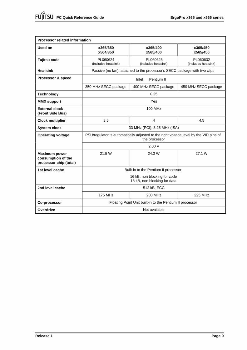
Processor related information
Used on x365/350x564/350
x365/400x565/400
x365/450x565/450
Fujitsu code PL060624(includes heatsink)
PL060625(includes heatsink)
PL060632(includes heatsink)
Heatsink Passive (no fan), attached to the processor’s SECC package with two clips
Processor & speed Intel Pentium II 350 MHz SECC package 400 MHz SECC package 450 MHz SECC package
Technology 0.25
MMX support Yes
External clock(Front Side Bus)
100 MHz
Clock multiplier 3.5 4 4.5
System clock 33 MHz (PCI), 8.25 MHz (ISA)
Operating voltage PSU/regulator is automatically adjusted to the right voltage level by the VID pins ofthe processor
2.00 V
Maximum powerconsumption of theprocessor chip (total)
21.5 W 24.3 W 27.1 W
1st level cache Built-in to the Pentium II processor:
16 kB, non blocking for code16 kB, non blocking for data
2nd level cache 512 kB, ECC
175 MHz 200 MHz 225 MHz
Co-processor Floating Point Unit built-in to the Pentium II processor
Overdrive Not available
Release 1 Page 9
ErgoPro x365 and x565 series PC Quick Reference Guide
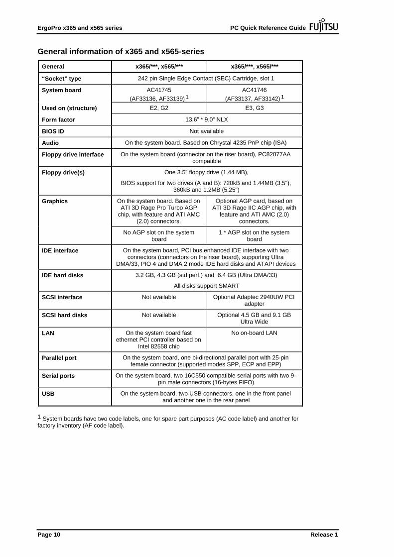
General information of x365 and x565-series
General x365/***, x565/*** x365/***, x565/***
“Socket” type 242 pin Single Edge Contact (SEC) Cartridge, slot 1
System board AC41745(AF33136, AF33139) 1
AC41746(AF33137, AF33142) 1
Used on (structure) E2, G2 E3, G3
Form factor 13.6” * 9.0” NLX
BIOS ID Not available
Audio On the system board. Based on Chrystal 4235 PnP chip (ISA)
Floppy drive interface On the system board (connector on the riser board), PC82077AAcompatible
Floppy drive(s) One 3.5” floppy drive (1.44 MB),
BIOS support for two drives (A and B): 720kB and 1.44MB (3.5"),360kB and 1.2MB (5.25")
Graphics On the system board. Based onATI 3D Rage Pro Turbo AGP
chip, with feature and ATI AMC(2.0) connectors.
Optional AGP card, based onATI 3D Rage IIC AGP chip, with
feature and ATI AMC (2.0)connectors.
No AGP slot on the systemboard
1 * AGP slot on the systemboard
IDE interface On the system board, PCI bus enhanced IDE interface with twoconnectors (connectors on the riser board), supporting Ultra
DMA/33, PIO 4 and DMA 2 mode IDE hard disks and ATAPI devices
IDE hard disks 3.2 GB, 4.3 GB (std perf.) and 6.4 GB (Ultra DMA/33)
All disks support SMART
SCSI interface Not available Optional Adaptec 2940UW PCIadapter
SCSI hard disks Not available Optional 4.5 GB and 9.1 GBUltra Wide
LAN On the system board fastethernet PCI controller based on
Intel 82558 chip
No on-board LAN
Parallel port On the system board, one bi-directional parallel port with 25-pinfemale connector (supported modes SPP, ECP and EPP)
Serial ports On the system board, two 16C550 compatible serial ports with two 9-pin male connectors (16-bytes FIFO)
USB On the system board, two USB connectors, one in the front paneland another one in the rear panel
1 System boards have two code labels, one for spare part purposes (AC code label) and another forfactory inventory (AF code label).
Page 10 Release 1
PC Quick Reference Guide ErgoPro x365 and x565 series
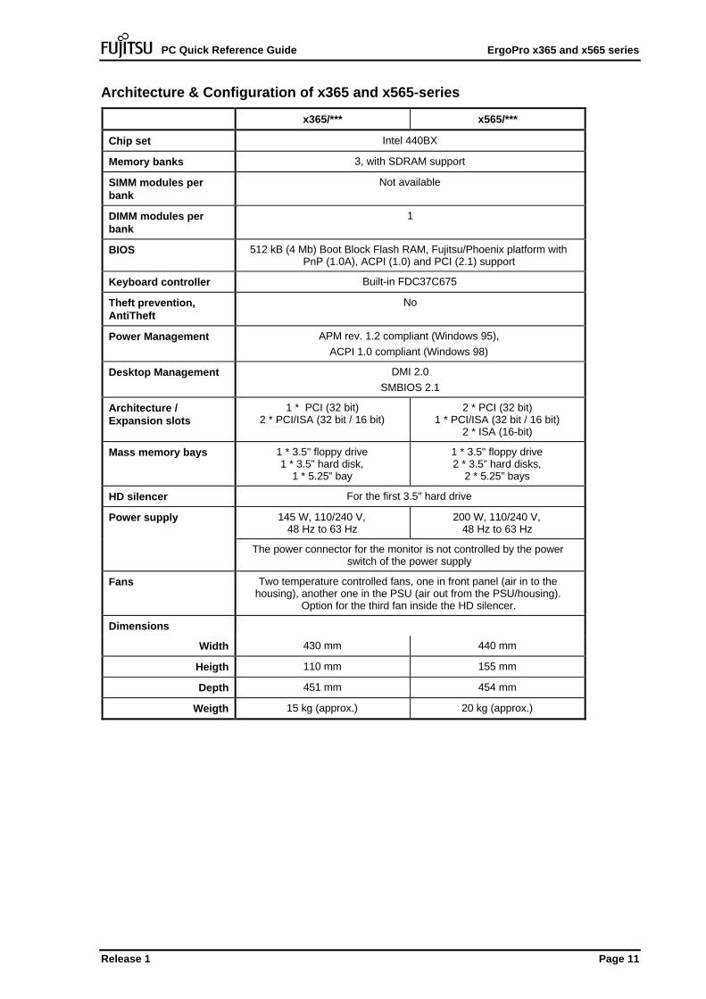
Architecture & Configuration of x365 and x565-series
x365/*** x565/***
Chip set Intel 440BX
Memory banks 3, with SDRAM support
SIMM modules perbank
Not available
DIMM modules perbank
1
BIOS 512 kB (4 Mb) Boot Block Flash RAM, Fujitsu/Phoenix platform withPnP (1.0A), ACPI (1.0) and PCI (2.1) support
Keyboard controller Built-in FDC37C675
Theft prevention,AntiTheft
No
Power Management APM rev. 1.2 compliant (Windows 95),ACPI 1.0 compliant (Windows 98)
Desktop Management DMI 2.0SMBIOS 2.1
Architecture /Expansion slots
1 * PCI (32 bit)2 * PCI/ISA (32 bit / 16 bit)
2 * PCI (32 bit)1 * PCI/ISA (32 bit / 16 bit)
2 * ISA (16-bit)
Mass memory bays 1 * 3.5" floppy drive1 * 3.5” hard disk,
1 * 5.25” bay
1 * 3.5" floppy drive2 * 3.5” hard disks,
2 * 5.25” bays
HD silencer For the first 3.5" hard drive
Power supply 145 W, 110/240 V,48 Hz to 63 Hz
200 W, 110/240 V,48 Hz to 63 Hz
The power connector for the monitor is not controlled by the powerswitch of the power supply
Fans Two temperature controlled fans, one in front panel (air in to thehousing), another one in the PSU (air out from the PSU/housing).
Option for the third fan inside the HD silencer.
Dimensions
Width 430 mm 440 mm
Heigth 110 mm 155 mm
Depth 451 mm 454 mm
Weigth 15 kg (approx.) 20 kg (approx.)
Release 1 Page 11

ErgoPro x365 and x565 series PC Quick Reference Guide
Memory configurations
Bank 0 Bank 1 Bank 2 Total Memory
32 MB - - 32 MB
32 MB 32 MB - 64 MB
64 MB - - 64 MB
32 MB 32 MB 32 MB 96 MB
32 MB 64 MB 96 MB
32 MB 32 MB 64 MB 128 MB
64 MB 64 MB - 128 MB
128 MB - - 128 MB
32 MB 64 MB 64 MB 160 MB
32 MB 128 MB 160 MB
32 MB 32 MB 128 MB 192 MB
64 MB 64 MB 64 MB 192 MB
64 MB 128 MB 192 MB
32 MB 64 MB 128 MB 224 MB
64 MB 64 MB 128 MB 256 MB
128 MB 128 MB - 256 MB
32 MB 128 MB 128 MB 288 MB
64 MB 128 MB 128 MB 320 MB
128 MB 128 MB 128 MB 384 MB
DIMM recommendations
DIMMsize (MB)
Description Speed Voltage Type Clocklines
Pins Module Kit code
32 4M*64 66 MHz 3.3V SDRAM 4 168 AF33852E
64 8M*64 66 MHz 3.3V SDRAM 4 168 AF33853E
128 16M*64 66 MHz 3.3V SDRAM 4 168 AF33854E
32 4M*64 100 MHz 3.3V SDRAM 4 168 AF33862E
64 8M*64 100 MHz 3.3V SDRAM 4 168 AF33863E
64 withECC
8M*72 100 MHz 3.3V SDRAM 4 168 AF33873E
128 16M*64 100 MHz 3.3V SDRAM 4 168 AF33864E
Page 12 Release 1
PC Quick Reference Guide ErgoPro x365 and x565 series
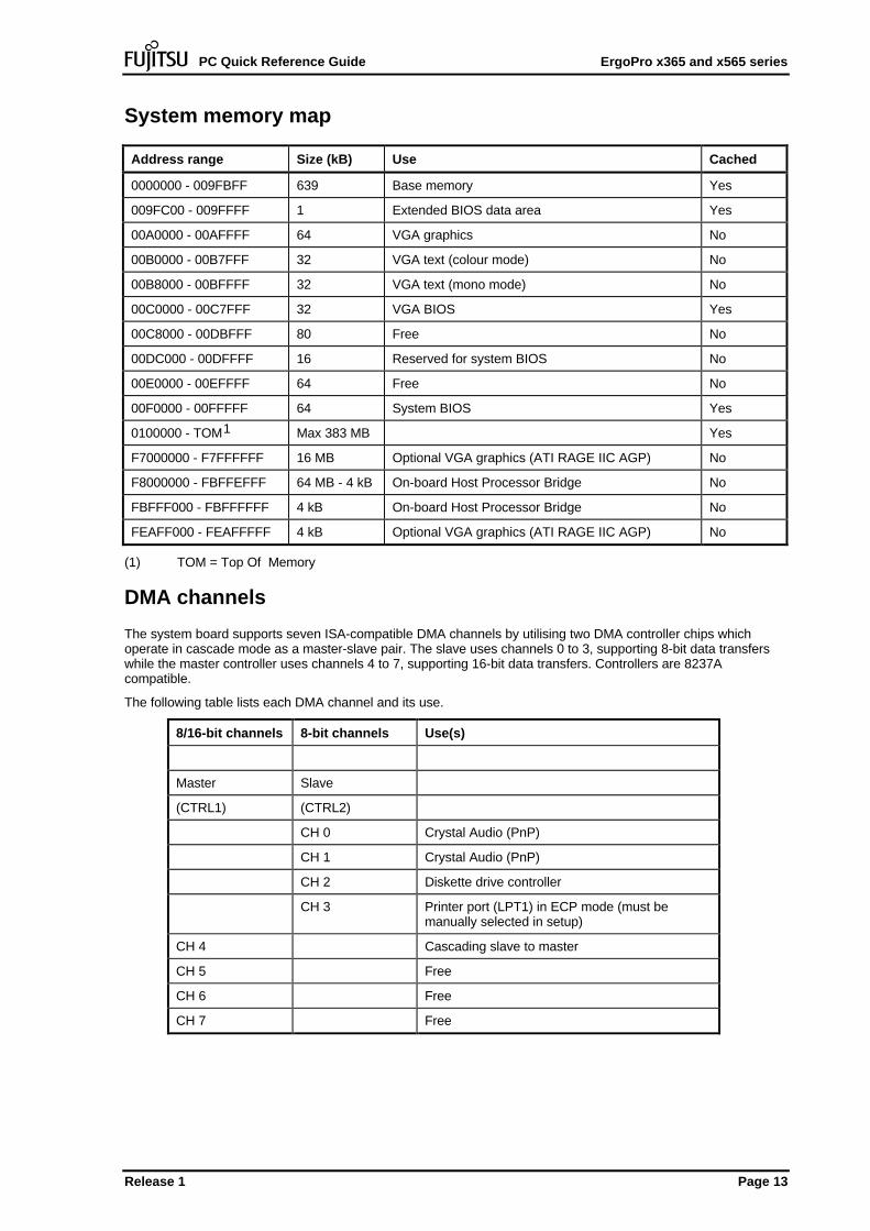
System memory map
Address range Size (kB) Use Cached
0000000 - 009FBFF 639 Base memory Yes
009FC00 - 009FFFF 1 Extended BIOS data area Yes
00A0000 - 00AFFFF 64 VGA graphics No
00B0000 - 00B7FFF 32 VGA text (colour mode) No
00B8000 - 00BFFFF 32 VGA text (mono mode) No
00C0000 - 00C7FFF 32 VGA BIOS Yes
00C8000 - 00DBFFF 80 Free No
00DC000 - 00DFFFF 16 Reserved for system BIOS No
00E0000 - 00EFFFF 64 Free No
00F0000 - 00FFFFF 64 System BIOS Yes
0100000 - TOM1 Max 383 MB Yes
F7000000 - F7FFFFFF 16 MB Optional VGA graphics (ATI RAGE IIC AGP) No
F8000000 - FBFFEFFF 64 MB - 4 kB On-board Host Processor Bridge No
FBFFF000 - FBFFFFFF 4 kB On-board Host Processor Bridge No
FEAFF000 - FEAFFFFF 4 kB Optional VGA graphics (ATI RAGE IIC AGP) No
(1) TOM = Top Of Memory
DMA channels
The system board supports seven ISA-compatible DMA channels by utilising two DMA controller chips whichoperate in cascade mode as a master-slave pair. The slave uses channels 0 to 3, supporting 8-bit data transferswhile the master controller uses channels 4 to 7, supporting 16-bit data transfers. Controllers are 8237Acompatible.
The following table lists each DMA channel and its use.
8/16-bit channels 8-bit channels Use(s)
Master Slave
(CTRL1) (CTRL2)
CH 0 Crystal Audio (PnP)
CH 1 Crystal Audio (PnP)
CH 2 Diskette drive controller
CH 3 Printer port (LPT1) in ECP mode (must bemanually selected in setup)
CH 4 Cascading slave to master
CH 5 Free
CH 6 Free
CH 7 Free
Release 1 Page 13
ErgoPro x365 and x565 series PC Quick Reference Guide
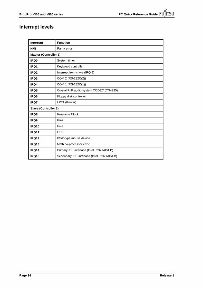
Interrupt levels
Interrupt Function
NMI Parity error
Master (Controller 1)
IRQ0 System timer
IRQ1 Keyboard controller
IRQ2 Interrupt from slave (IRQ 9)
IRQ3 COM 2 (RS-232C(2))
IRQ4 COM 1 (RS-232C(1))
IRQ5 Crystal PnP audio system CODEC (CS4235)
IRQ6 Floppy disk controller
IRQ7 LPT1 (Printer)
Slave (Controller 2)
IRQ8 Real-time Clock
IRQ9 Free
IRQ10 Free
IRQ11 USB
IRQ12 PS/2-type mouse device
IRQ13 Math co-processor error
IRQ14 Primary IDE interface (Intel 82371AB/EB)
IRQ15 Secondary IDE interface (Intel 82371AB/EB)
Page 14 Release 1

PC Quick Reference Guide ErgoPro x365 and x565 series
BIOS update
The BIOS code is stored in a 4 Mb (512 kB) boot block Flash RAM soldered on the system board. This allowsBIOS updates through software, without the need to replace any hardware components, using the Phlash.exeprogram.
A bootable DOS floppy is needed for the BIOS update. The floppy must have the following files :
-Phlash.exe-Platform.bin, and-M63vxxx.rom, where xxx stands for the BIOS version; for instance, 107 = version 1.07),
To update the BIOS, type
phlash m63vxxx.rom
The update is performed automatically. During update, Phlash.exe displays a progress indicator on the screen.When the update procedure is complete, a status window appears showing whether or not the update wassuccessful.
Force Flash Load
It is unlikely that anything will interrupt the Flash upgrade procedure. However, if an interruption occurs thatprevents the upgrade from continuing, it is possible that the BIOS will be left in an unusable state. In thissituation, a BIOS recovery procedure called "Force Flash Load" might be able to restore the BIOS code in theFlash RAM.
On x365/*** and x565/***, the Force Flash Load operation is automatic; there are no jumpers for this purpose.Force Flash Load is started during the POST when the loader part (normally write-protected by jumper JP14 onthe system board) of the system BIOS checks the BIOS modules and tests their condition. If the test finds anycritical errors, which might stop the system POST or hang the system during or before loading the operatingsystem, it starts the Force Flash Load procedure.
Note Due to the limited amount of code available in the non-erasable boot block area, no on-screen messages are displayed to direct the flash recovery. To monitor the progress of the Force Flash Load operation, pay attention to the beep codes that the system issues on the speaker during the procedure.
The following beep codes, which are sequencies of long and short beeps, inform the user of the progress of theForce Flash Load recovery: Short beeps are indicated with • and long beeps with - .
•- • • Content of the Flash RAM is corrupted.
• • • Cannot read the floppy- Programming successfully completed
The automatic Force Flash Load procedure starts with the error code •- • • ("Content of the Flash RAM iscorrupted"). The system sounds this beep code about five seconds after the system unit been switched on.
The first error code is followed by another after a second; this is the error code • • • ("Cannot read the floppy").This code indicates that a floppy with the proper BIOS files and utilities needs to be inserted in the floppy drive.After this is done, the BIOS recovery is started automatically, which is indicated by the fact that error messagethe • • • ("Cannot read the floppy") is replaced by a sequence of short beeps ( •), with a beep sounded every oneor two seconds for the duration of 50 to 70 seconds.
When the Force Flash Load procedure is complete, the system sounds one short and one long beep ( •-), afterwhich the floppy disk can be removed from the floppy drive.
To successfully complete the Force Flash operation, the x365/x565 BIOS Force Flash Load floppy with thefollowing BIOS specific files is needed:
- MiniDOS.sys- Phlash.exe- Platform.bin, and- BIOS.rom.
Release 1 Page 15
ErgoPro x365 and x565 series PC Quick Reference Guide
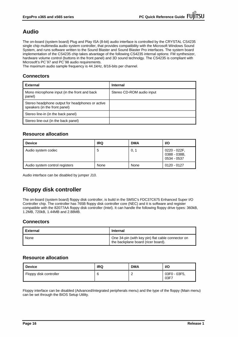
Audio
The on-board (system board) Plug and Play ISA (8-bit) audio interface is controlled by the CRYSTAL CS4235single chip multimedia audio system controller, that provides compatibility with the Microsoft Windows SoundSystem, and runs software written to the Sound Blaster and Sound Blaster Pro interfaces. The system boardimplementation of the CS4235 chip takes atvantage of the following CS4235 internal options: FM synthesizer,hardware volume control (buttons in the front panel) and 3D sound technolgy. The CS4235 is compliant withMicrosoft’s PC´97 and PC´98 audio requirements.The maximum audio sample frequency is 44.1kHz, 8/16-bits per channel.
Connectors
External Internal
Mono microphone input (in the front and backpanel)
Stereo CD-ROM audio input
Stereo headphone output for headphones or activespeakers (in the front panel)
Stereo line-in (in the back panel)
Stereo line-out (in the back panel)
Resource allocation
Device IRQ DMA I/O
Audio system codec 5 0, 1 0220 - 022F,0388 - 038B,0534 - 0537
Audio system control registers None None 0120 - 0127
Audio interface can be disabled by jumper J10.
Floppy disk controller
The on-board (system board) floppy disk controller, is build in the SMSC's FDC37C675 Enhanced Super I/OController chip. The controller has 765B floppy disk controller core (NEC) and it is software and registercompatible with the 82077AA floppy disk controller (Intel). It can handle the following floppy drive types: 360kB,1.2MB, 720kB, 1.44MB and 2.88MB.
Connectors
External Internal
None One 34-pin (with key pin) flat cable connector onthe backplane board (ricer board).
Resource allocation
Device IRQ DMA I/O
Floppy disk controller 6 2 03F0 - 03F5,03F7
Floppy interface can be disabled (Advanced/integrated peripherals menu) and the type of the floppy (Main menu)can be set through the BIOS Setup Utility.
Page 16 Release 1
PC Quick Reference Guide ErgoPro x365 and x565 series
Graphics (on-board)
The on-board AGP bus graphics is controlled by an ATI 3D Rage Pro Turbo AGP chip with 4MB of SGRAM,which is not expandable. The ATI 3D Rage Pro Turbo AGP has a build-in RAMDAC, which can handle pixelfrequencies up to 230 MHz.
The ATI 3D Rage Pro Turbo AGP is a 64-bit video engine, which is connected directly to the 32-bit on-board AGPbus, and supports following AGP features: 1X and 2X mode, sideband addressing, AGP texturing (executemode) and pipelining. With 4 MB of SGRAM, the ATI 3D Rage IIC AGP chip can utilize 64-bit data path betweenthe chip and the graphics memory. The graphics interface is DDC2B compatible. The On-board graphicscontroller is automatically disabled by the plug and play BIOS when another video board (PCI or ISA) is installed.
Refresh ratesMaximum defined refresh rates for the graphics chip.
Video controller Video Memory Resolutions
640*480 800*600 1024*768 1280*1024 1600*1200
On-board 200/24 200/24 150/24 100/24 85/16
graphics based on 4 MB (SGRAM)
ATI 3D Rage ProTurbo
200/24 = Refresh rate is 200 Hz and there are 24 Bits per Pixel
Note! The actual refresh rate is directly related to the monitor in use (do not exceed monitor specifications), andmay vary between operating systems.
Graphics memory upgrades for the on-board adapter
Graphicsmemory on thesystem board
Memoryupgrademodule
Module codefor the upgrademodule
kit code for theupgrademodule
Total videomemory
System boards
4 MB (SGRAM) N/A1 N/A1 N/A1 4 MB (SGRAM)
1 N/A = Not Available, the memory of the on-board graphics controller can not be upgraded
Connectors
External Internal
One 15-pin (standard) VGA connector at the backpanel of the system unit
Video feature connector with AMC extension
Resource allocation
Device IRQ DMA Memory I/O
ATI 3D Rage Pro Turbo AGP None None 000A0000 - 000AFFFF000B0000 - 000BFFFF
03B0 - 03BB03C0 - 03DF9000 - 90FF
Release 1 Page 17
ErgoPro x365 and x565 series PC Quick Reference Guide
IDE interface
There are two enhanced PCI (master mode) bus IDE controllers/interfaces on the system board (build in the IntelPIIX4e (82371EB)) which can handle up to four IDE devices. The 82371EB supports PIO modes 0 to 4, DMAmultiword mode 2 timing and Ultra DMA 33 mode, in addition the PIIX4e has an integrated 16 * 32-bit buffer tosupports IDE PCI burst transfers. Both the primary and the secondary IDE bus can handle up to 2 hard drives orother IDE devices. The BIOS has support for ATAPI devices and it also supports booting from the CD-ROM.
Connectors
External Internal
None Two 40-pin (with key pin) flat cable connectors onthe backplane board (ricer board)
Resource allocation
Device IRQ DMA I/O
Primary IDE channel 14 None 01F0 - 01F703F6FCD0 - FCDF
Secondary IDE channel 15 None 0170 - 01770376FCD0 - FCDF
The on-board IDE interface(s) can be Enabled/Disabled from the BIOS SETUP Utility (Advanced/Integratedperipherals menu).
Parallel port communication
There is one multi-mode parallel port build in the FDC37C675 super I/O chip, which supports following modes:
Output only :
Bi-directional (SPP) : IBM PC/XT, PC/AT, and PS/2 compatible bi-directional parallel port.
EPP (Enhanced mode) : Enhanced Parallel Port (EPP 1.9), and is IEEE1284 compliant.
ECP (High speed mode) : Microsoft and Hewlett Packard Extended Capabilities Port, and is IEEE1284compliant.
The parallel port mode can be set through the BIOS Set-up Utility (Advanced/integrated peripherals menu).
Connectors
External Internal
One standard 25-pin D-type connector in the backpanel of the system housing (on the system board)
None
Resource allocation
Device IRQ DMA I/O
Printer port LPT1 (output only, bi-directional and EPP modes)
7 None 0378 - 037F
Printer port LPT1 (ECP mode) 7 3 (recommendedsetting)
0378 - 037F0778 - 077F
The on-board parallel port can be configured to LPT1 (378, IRQ 7 or 5), LPT2 (278, IRQ 7 or 5), LPT3 (3BC, IRQ7 or 5) and disabled through the BIOS SETUP Utility (Advanced/integrated peripherals menu).
Page 18 Release 1
PC Quick Reference Guide ErgoPro x365 and x565 series
PS/2 type Keyboard & mouse
The controller of the PS/2-type keyboard and mouse is build in the SMSC's FDC37C675 super I/O controller, andprovides software compatibility with the 8042A microcontrollers.
Connectors
External Internal
One 6-pin PS/2 type connector for keyboard None
One 6-pin PS/2 type connector for mouse None
Resource allocation
Device IRQ DMA I/O
PS/2 Keyboard 1 None 00600064
PS/2 Mouse 12 None None
Serial port communication
It comprises 2 high speed NS16C550 compatible UARTs with send/receive 16 Byte FIFOs. The UARTs areplaced in the FDC37C675.
The maximum transfer speed supported by the BIOS functions is 19200 bps, and by the HW 115 kbps.Instant on-function wakes up the system when the modem generates the Ring Indicator signal.
Connectors
External Internal
Two standard 9-pin D-type connector (RS-232C) inthe back panel of the system housing (on thesystem board)
None
Resource allocation
Device IRQ DMA I/O
Communication port COM1 4 None 03F8 - 03FF
Communication port COM2 3 None 02F8 - 02FF
The on-board serial ports can be configured to COM1 (3F8, IRQ 4 or 11), COM2 (2F8, IRQ 3 or 10), COM3 (3E8,IRQ 4 or 11), COM4 (2E8, IRQ 3 or 10) or it can be disabled through the BIOS Setup Utility (Advanced/integratedperipherals menu).
Release 1 Page 19
ErgoPro x365 and x565 series PC Quick Reference Guide
Peripheral Component Interconnect (PCI interface)
The PCI bus controller build in the Intel 82443BX chip (440BX AGP set) connects the CPU bus (front side bus) tothe PCI bus in asynchronous mode and provides the maximum speed of 33 MHz for the PCI bus. The hardwareand the BIOS are compliant to the version 2.1 of the PCI specification (+5 V 33 MHz) and has support for fivePCI master devices and PCI to PCI bridge.
Connectors
External Internal
None x365/*** system unitsThree 32-bit PCI bus slots (two shared with theISA slots)
x565/*** system unitsThree 32-bit PCI bus slots (one shared with theISA slot)
Accelerated Graphics Port (AGP interface)
The AGP bus controller build in the Intel 82443BX chip (440BX AGP set) connects the CPU bus (front side bus)to the AGP bus in asynchronous (100 MHz Front side bus, synchronous for 66.7 MHz Front side bus) mode andprovides the maximum speed of 66/133 MHz for the AGP bus. The hardware and the BIOS are compliant to theversion 1.0 of the AGP specification (+3.3 V 66 MHz).
Connectors
External Internal
None System boards with on-board AGP graphics:None, AGP interface is used for the on-board ATI3D Rage Pro Turbo AGP graphics controller
System boards w/o on-board AGP graphics:One AGP slot connector on the system board
USB
On the system board there are two 4-pin USB connectors (ports), one in the front panel and another in the rearpanel, for serial transfers at 12 or 1.5 Mbps, controlled by the USB Host Controller (HC) built-in the 82371EB(PIIX4e) chip. The Host Controller includes the root hub with two USB ports and it supports the standardUniversal Host Controller Interface (UHCI).
If more than two USB devices are required, an external hub can be connected to either of the on-board USBports.
Connectors
External Internal
Two 4-pin USB connectors, one at the back panelof the system unit and another in the front panel.
None
Resource allocation
Device IRQ DMA Memory I/O
USB 11 None None FCE0 - FCFF
USB interface can not be configured throught BIOS setup utility.
Page 20 Release 1
PC Quick Reference Guide ErgoPro x365 and x565 series
Ethernet Controller (on-board)
The on-board PCI Fast Ethernet Local Area Network controller is compatible with the Intel EtherExpressPRO/100+ adapter. The controller is build around the Intel 82558 Fast Ethernet PCI bus LAN controller chip withbuild-in 10/100 BASE Physical Layer interface (PHY), 3 kB transmit and 3 kB receive FIFOs, 32-bit PCI interfaceand a Magic Packet support (Wake On LAN support).
The Ethernet interface can be connected to a Twisted Pair (TP) cable through an 8-pin RJ45 connector. It ispossible to use the module in 10Mbps or 100Mbps Twisted Pair Ethernet LAN by simply connecting the networkadapter to a 10BASE-T or 100BASE-T hub port. By default the Fast Ethernet module automatically identifies thespeed of the hub port and configures itself to the right speed without any hardware or software changes.
Wake On LAN support is provided by the build-in Magic Packet "filter" of the Intel 82558 chip, for which the plusfive (+5 V) volt stand-by voltage is always supplied.
Remote Boot options:The system BIOS includes LANDesk Service Agent (LSA) and provides Intel Preboot eXecution Environment(PXE). When network boot is enabled (Boot menu), system tries to load the boot image from a remoteBOOTP/TFTP server.
Connectors
External Internal
8 pin RJ45 connector None
Resource allocation
Device IRQ DMA Memory I/O
None None
Network interface can not be configured through BIOS setup utility.
LED board
The LED board has three indicators that are located on the front panel, from top to bottom:
POWER (Green) Illuminated when the system is switched ON.HDD (Yellow) Illuminated during HDD activity.Message waitting (Red) This LED is not used (not connected)
Release 1 Page 21
ErgoPro x365 and x565 series PC Quick Reference Guide
Power On Self Test (POST)
After the power has been turned on, the system performs a power on self-test to check that all parts are workingproperly. If the test does not find any faults, BIOS tries to load the operating system.
During the POST Fujitsu logo is shown on the screen until Operating System starts and shows it’s own logo.If <ESC> key is pressed while the Fujitsu logo is shown on the screen, the logo screen is changed to thefollowing text screen (basic settings) that is shown on the screen until Operating System starts. The informationshown on the screen is updated line by line and the information shown may vary between different hardwareconfigurations and BIOS settings.
PhoenixBIOS Version 4.05Copyright 1985-1998 Phoenix Technologies Ltd., All Rights Reserved.
Fujitsu Desktop BIOS Version 1.07Copyright FUJITSU LIMITED 1995-1998.
CPU = Pentium(R) II processor 350 MHz0640K System RAM Passed0063M Extended RAM Passed0512K Cache SRAM PassedSystem BIOS shadowedVideo BIOS shadowedMouse initialized
Press <F2> to enter SETUP
The text screen indicates the BIOS version (1.07), type and speed of the CPU, total amount of system (0640 kilobytes) and extended (0063 mega bytes) memory installed and the size of the cache (0512 kB) in the system. Italso indicates if PS/2 type mouse has been found and initiliazed.
If the self-test finds any faults, indication of that is shown one of the following two ways:
• You will hear two short beeps ( • •) and see a message on the screen.• You will hear a sequence of long and short beeps immediately after you have started the system.
The following pages describe the steps that you should take if either fault situation should occur.
Page 22 Release 1
PC Quick Reference Guide ErgoPro x365 and x565 series
Two short beeps and a messageThe format these messages take is:
Short description ---> Operating system not found
If you see a message that does not have this format, it probably comes from an additional board installed in thesystem unit. For further information, refer to the documentation of the board .
If the keyboard is concerned, the start-up procedure will continue after a while. Otherwise, you will see thismessage:
Press <F1> to resume, <F2> to SETUP.
Pressing F1 allows you to bypass the fault without correcting it. Enter SETUP by pressing F2 , and check thatthe configuration parameters are correct.
Should the message persist, check the following list, and contact service.
List of error messages:
Diskette drive [A / B] errorDrive A: or B: is present but fails the BIOS POST diskette tests. Check to see that the drive is defined withthe proper diskette type in Setup and that the diskette drive is attached correctly.
[DMA / IO / IRQ / MEM] Allocation Error-Function #:xxExecute ISA configuration utility (ICU) and set the proper settings such as DMA channel and so on.
Extended RAM Failed at offest: nnnnExtended memory not working or not configured properly. Check if the extended memory is attachedproperly.
Failing Bits: nnnnThe hex number nnnn is a map of the bits at the RAM address (in System, Extended or Shadow memory)which failed the memory test. Each 1 (one) in the map indicates a failed bit. Check if extended memory isattached properly.
Failure Fixed Disk [0 / 1 / 2 / 3]Fixed disk is not working or not configured properly. Check to see if fixed disk and flat cable are attachedproperly. Run Setup to ensure that the fixed-disk type is correctly identified.
[Fixed Disk / Diskette Drive] address confilictOption card and fixed disk/diskette drive addresses are conflict. Change ISA card address.
Incorrect Drive [A / B] type - run SETUPType of floppy drive [A / B]: not correctly identified in Setup. Select proper type of diskette in Setup.
Invalid NVRAM media typeProblem with NVRAM access.
Keyboard controller errorThe keyboard controller failed test. You may have to replace keyboard or controller.
Keyboard errorKeyboard not working. Check if keyboard is connected properly.
Operating system not foundOperating system cannot be located on either drive A: or drive C:. Enter Setup and see if fixed disk anddrive A: are properly identified.
Parity Check [1 / 2]Parity error found in the [system or I/O] bus. BIOS attempts to locate the address and display it on thescreen.
Press <F1> to resume, <F2> to SetupDisplayed after any recoverable error message. Press <F1> to start the boot process or <F2> to enterSetup and change any settings.
Release 1 Page 23

ErgoPro x365 and x565 series PC Quick Reference Guide
Press <F2> to enter SETUPOptional message displayed during POST. Can be turned off in Setup.
Previous boot incomplete - Default configuration usedPrevious POST did not complete successfully. POST loads default values and offers to run Setup. If thefailure was caused by incorrect values and they are not corrected, the next boot will likely fail. On systemswith control of wait states, improper Setup settings can also terminate POST and cause this error on thenext boot. Run Setup and verify that the wait-state configuration is correct. This error is cleared the nexttime the system is booted.
PXE-E52:No IP address received from DHCP or BOOTP.PXE-M0F:Exiting LANDesk (R) Service Agent IIPreboot Execution Environment (PXE) error. PXE could not get IP address. Prepare the installation serverwhich is Network PC System Design Guidelines Version 1.0b compliant or disable Preboot ExecutionEnvironment in Setup.
PXE-T01:File not foundPXE-E3B:TFTP Error - File Not foundPXE-M0F:Exiting LANDesk (R) Service Agent IIPreboot Execution Environment (PXE) error. PXE could not get boot file name from server. Prepare theinstallation server which is Network PC System Design Guidelines Version 1.0b compliant or disablePreboot Execution Environment in Setup.
PXE-E61:Media test failure,check cable.PXE-M0F:Exiting LANDesk (R) Service Agent IIPreboot Execution Environment (PXE) error. LAN cable is not connected properly. Check if LAN cable isconnected properly or disable Preboot Execution Environment in Setup.
Real time clock errorReal-time clock fails BIOS test. May require board repair.
Shadow Ram Failed at offest: nnnnShadow RAM failed at offset nnnn of the 64k block at which the error was detected.
Stuck KeyBIOS discovered a stuck key. Check if keyboard is attached properly or if some key is kept pressed.
System battery is dead - Replace and run SETUPThe CMOS clock battery indicator shows the battery is dead. Replace the battery and run Setup toreconfigure the system.
System cache error - Cache disabledRAM cache failed the BIOS test. BIOS disabled the cache.
System CMOS checksum bad - run SETUPSystem CMOS has been corrupted or modified incorrectly, perhaps by an application program thatchanges data stored in CMOS. Run Setup and reconfigure the system.
System RAM Failed at offest: nnnnSystem RAM failed at offset nnnn of in the 64k block at which the error was detected. Check if memory isattached properly.
System time errorThe timer test failed. Requires repair of system board.
xxxh [COM / LPT] address conflictOption card and serial/parallel port address are conflict. Change serial/parallel port address in Setup orchange ISA card address.
Page 24 Release 1
PC Quick Reference Guide ErgoPro x365 and x565 series
Sequences of long and short beepsIf you hear a sequence of long and short beeps immediately after you have started the system, the self-test hasdetected an equipment failure. Turn all units off, check their connections, and try again. If you hear the sequenceagain, write it down, and call our local service representative.
The following list contains the signal sequences. Short beeps are indicated with •, long beeps with - and spacebetween beeps with _. I/O port 80h message numbers are shown in brackets.
Short beeps
• 1 (B4h and F4h) No errors found during POST, operating system will be loaded.
•_• •_• •_• • • 1-2-2-3 (16h) BIOS ROM checksum.•_• • •_•_• 1-3-1-1 (20h) Test DRAM refresh.•_• • •_•_• • • 1-3-1-3 (22h) Test 8742 keyboard controller•_• • •_• • • •_• 1-3-4-1 (2Ch) RAM failure on address line.•_• • •_• • • •_• • • 1-3-4-3 (2Eh) RAM failure on data bits of low byte of memory bus.•_• • • •_•_• 1-4-1-1 (30h) RAM failure on data bits of high byte of memory bus.• •_•_• •_• • • 2-1-2-3 (46h) Check ROM copyright notice.• •_• •_• • •_• 2-2-3-1 (58h) Test for unexpected interrupts.
Long and short beeps
- _• • 1-2 (98h) Search for option ROMs, checksum error.
Release 1 Page 25
ErgoPro x365 and x565 series PC Quick Reference Guide
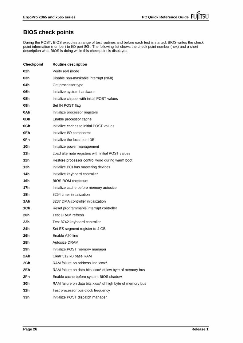
BIOS check points
During the POST, BIOS executes a range of test routines and before each test is started, BIOS writes the checkpoint information (number) to I/O port 80h. The following list shows the check point number (hex) and a shortdescription what BIOS is doing while this checkpoint is displayed.
Checkpoint Routine description
02h Verify real mode
03h Disable non-maskable interrupt (NMI)
04h Get processor type
06h Initialize system hardware
08h Initialize chipset with initial POST values
09h Set IN POST flag
0Ah Initialize processor registers
0Bh Enable processor cache
0Ch Initialize caches to initial POST values
0Eh Initialize I/O component
0Fh Initialize the local bus IDE
10h Initialize power management
11h Load alternate registers with initial POST values
12h Restore processor control word during warm boot
13h Initialize PCI bus mastering devices
14h Initialize keyboard controller
16h BIOS ROM checksum
17h Initialize cache before memory autosize
18h 8254 timer initialization
1Ah 8237 DMA controller initialization
1Ch Reset programmable interrupt controller
20h Test DRAM refresh
22h Test 8742 keyboard controller
24h Set ES segment register to 4 GB
26h Enable A20 line
28h Autosize DRAM
29h Initialize POST memory manager
2Ah Clear 512 kB base RAM
2Ch RAM failure on address line xxxx*
2Eh RAM failure on data bits xxxx* of low byte of memory bus
2Fh Enable cache before system BIOS shadow
30h RAM failure on data bits xxxx* of high byte of memory bus
32h Test processor bus-clock frequency
33h Initialize POST dispatch manager
Page 26 Release 1

PC Quick Reference Guide ErgoPro x365 and x565 series
Checkpoint Routine description
36h Warm start shut down
38h Shadow system BIOS ROM
3Ah Autosize cache
3Ch Advanced Configuration of chipset registers
3Dh Load alternate registers with CMOS values
42h Initialize interrupt vectors
45h POST device initialization
46h Check ROM copyright notice
48h Check video configuration against CMOS RAM data
49h Initialize PCI bus and devices
4Ah Initialize all video adapters in system
4Bh Display QuietBoot screen
4Ch Shadow video BIOS ROM
4Eh Display BIOS copyright notice
50h Display processor type and speed
51h Initialize EISA board
52h Test keyboard
54h Set key click if enabled
58h Test for unexpected interrupts
59h Initialize POST display service
5Ah Display prompt "Press F2 to enter SETUP"
5Bh Disable processor cache
5Ch Test RAM between 512 and 640 kB
60h Test extended memory
62h Test extended memory address lines
64h Jump to UserPatch1
66h Configure advanced cache registers
67h Initialize multiprocessor APIC
68h Enable external and processor caches
69h Setup System Management Mode (SMM) area
6Ah Display external L2 cache size
6BH Load custom defaults
6Ch Display shadow-area message
6Eh Display possible high address for UMB recovery
70h Display error messages
72h Check for configuration errors
76h Check for keyboard errors
7Ch Set up hardware interrupt vectors
7Eh Initialize coprocessor if present
80h Disable onboard Super I/O ports and IRQs
81h Late POST device initialization
Release 1 Page 27

ErgoPro x365 and x565 series PC Quick Reference Guide
Checkpoint Routine description
82h Detect and install external RS232 ports
83h Configure non-MCD IDE controllers
84h Detect and install external parallel ports
85h Initialize PC-compatible PnP ISA devices
86h Re-initialize onboard I/O ports
87h Configure motherboard configurable devices
88h Initialize BIOS Data Area
89h Enable Non-Maskable Interrupts (NMIs)
8Ah Initialize extended BIOS data area
8Bh Test and initialize PS/2 mouse
8Ch Initialize floppy controller
8Fh Determine number of ATA drives
90h Initialize hard-disk controllers
91h Initialize local-bus hard-disk controllers
92h Jump to UserPatch2
93h Build MPTABLE for multiprocessor boards
95h Install CD ROM for boot
96h Clear huge ES segment register
97h Fix up multiprocessor table
98h Search for option ROMs
99h Check for SMART Drive
9Ah Shadow option ROMs
9Ch Set up power management
9Dh Initialize security manager
9Eh Enable hardware interrupts
9Fh Determine number of ATA and SCSI drives
A0h Set time of day
A2h Check key lock
A4h Initialize typematic rate
A8h Erase F2 prompt
AAh Scan for F2 key stroke
ACh Enter SETUP
AEh Clear IN POST flag
B0h Check for errors
B2h POST done - prepare to boot operating system
B4h One short beep before boot
B5h Terminate QuietBoot
B6h Check password
B9h Prepare boot
BAh Initialize DMI parameters
BBh Initialize PnP Option ROMs
Page 28 Release 1

PC Quick Reference Guide ErgoPro x365 and x565 series
Checkpoint Routine description
BCh Clear parity checkers
BDh Display MultiBoot menu
BEh Clear screen
BFh Check virus and backup reminders
C0h Try to boot with INT 19
C1h Initialize POST Error Manager (PEM)
C2h Initialize error logging
C3h Initialize error display function
C4h Initialize system error handler
C5h PnP and dual CMOS
C8h Force check
C9h Extended checksum
D2h Unknown interrupt
Release 1 Page 29

ErgoPro x365 and x565 series PC Quick Reference Guide
Checkpoint BIOS Boot block Routine description
E0h Initialize the chipset
E1h Initialize the bridge
E2h Initialize the processor
E3h Initialize system timer
E4h Initialize system I/O
E5h Check force recovery boot
E6h Checksum BIOS ROM
E7h Go to BIOS
E8h Set huge segment
E9h Initialize multiprocessor
EAh Initialize OEM special code
EBh Initialize PIC and DMA
ECh Initialize memory type
EDh Initialize memory size
EEh Shadow boot block
EFh System memory test
F0h Initialize interrupt vectors
F1h Initialize run time clock
F2h Initialize video
F3h Initialize System Management Mode
F4h Output one beep before boot
F5h Boot to mini-DOS
F6h Clear huge segment
F7h Boot to full DOS
Page 30 Release 1

PC Quick Reference Guide ErgoPro x365 and x565 series
e365/*** and x565/***structure codes
Every unit has an identification label located in the system unit. The picture below shows the location of theidentification label on 3-slot and 5-slot housings.
This code can be divided into eleven parts, indicating that way the exact configuration of the machine. Thefollowing pages are explaining those codes.
Product :
1 to 2 : Product family3. Processor type4. Option boards
5. Hard Disk
6. Other massmemories
11. Keyboard layout
10. Keyboard
9. Operating system
8. PI-language + manual
7. RAM
E3 30 2 E0 7 E1
12. Country (mains cable)
1G
Release 1 Page 31

ErgoPro x365 and x565 series PC Quick Reference Guide
Identification codes
The following code information should be used for product identification only. The information should not be usedto build up an ordering code.
1-2. PRODUCT FAMILYThe letter(s) in brackets () is/are for the third digit System board code
E2(E) x365/266 Pentium II (Audio, LAN, Graphics) AC41745E2(F) x365/300 Pentium II (Audio, LAN, Graphics) AC41745E2(G) x365/333 Pentium II (Audio, LAN, Graphics) AC41745E2(H) x365/350 Pentium II (Audio, LAN, Graphics) AC41745E2(J) x365/400 Pentium II (Audio, LAN, Graphics) AC41745E2(R) x365/450 Pentium II (Audio, LAN, Graphics) AC41745
E3(F) x365/300 Pentium II (Audio, no LAN, no Graphics) AC41746E3(G) x365/333 Pentium II (Audio, no LAN, no Graphics) AC41746E3(H) x365/350 Pentium II (Audio, no LAN, no Graphics) AC41746E3(J) x365/400 Pentium II (Audio, no LAN, no Graphics) AC41746E3(R) x365/450 Pentium II (Audio, no LAN, no Graphics) AC41746
G2(F) x565/300 Pentium II (Audio, LAN, Graphics) AC41745G2(G) x565/333 Pentium II (Audio, LAN, Graphics) AC41745G2(H) x565/350 Pentium II (Audio, LAN, Graphics) AC41745G2(J) x565/400 Pentium II (Audio, LAN, Graphics) AC41745G2(R) x565/450 Pentium II (Audio, LAN, Graphics) AC41745
G3(F) x565/300 Pentium II (Audio, no LAN, no Graphics) AC41746G3(G) x565/333 Pentium II (Audio, no LAN, no Graphics) AC41746G3(H) x565/350 Pentium II (Audio, no LAN, no Graphics) AC41746G3(J) x565/400 Pentium II (Audio, no LAN, no Graphics) AC41746G3(R) x565/450 Pentium II (Audio, no LAN, no Graphics) AC41746
3. PROCESSOR & HEATSINKE 266 MHz Pentium II CPUF 300 MHz Pentium II CPUG 333 MHz Pentium II CPUH 350 MHz Pentium II CPUJ 400 MHz Pentium II CPUR 450 MHz Pentium II CPU
4. OPTION BOARDS0 No option board(s)2 ATI 3D RAGE IIC AGP AF31559
5. HARD DRIVE6 3.2 GB IDE hard drive AF212327 4.3 GB IDE hard drive AF212338 6.4 GB IDE hard drive AF21234
6. OTHER MASSMEMORIES0 No other massmemoriesD 24x IDE CD-ROM drive AF23337
7. RAM2 1 * 32 MB 66 MHz SDRAM DIMM (non-ECC) AF33852E3 1 * 32 MB 100 MHz SDRAM DIMM (non-ECC) AF33862E4 1 * 64 MB 66 MHz SDRAM DIMM (non-ECC) AF33853E6 1 * 64 MB 100 MHz SDRAM DIMM (non-ECC) AF33863E
Page 32 Release 1

PC Quick Reference Guide ErgoPro x365 and x565 series
8. PI-LANGUAGE + MANUALE EnglishF DanishG GermanH SpanishJ FrenchK DutchL NorwegianM FinnishN SwedishP PortugueseS Italian
9. OPERATING SYSTEM2 Windows 953 Windows NT 4.06 Windows 98
10. KEYBOARD0 No keyboard1 e105
11. KEYBOARD LAYOUT0 No keyboardA Hungarian 105E English e105F Danish e105G German e105H Spanish e105J French e105K Dutsh e105L Norwegian e105M Finnish e105N Swedish e105P Portuguese e105S Italian 105V Czech 105Y Polish 1052 Belgium e1053 USA e105
12 COUNTRY (MAINS CABLE + MOUSE)0 No cable, no mouse1 EU cable, Fujitsu2 EU cable, MikroMikko3 UK cable, Fujitsu5 DK cable, Fujitsu6 CH cable, Fujitsu7 US cable, Fujitsu8 IT cable, FujitsuA AUS cable FujitsuB South Africa
Release 1 Page 33
ErgoPro x365 and x565 series PC Quick Reference Guide
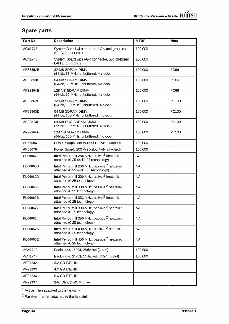
Spare parts
Part No Description MTBF Note
AC41745 System Board with on-board LAN and graphics,w/o AGP connector
100 000
AC41746 System Board with AGP connector, w/o on-boardLAN and graphics
100 000
AF33852E 32 MB SDRAM DIMM(64-bit, 66 MHz, unbuffered, 4-clock)
100 000 PC66
AF33853E 64 MB SDRAM DIMM(64-bit, 66 MHz, unbuffered, 4-clock)
100 000 PC66
AF33854E 128 MB SDRAM DIMM(64-bit, 66 MHz, unbuffered, 4-clock)
100 000 PC66
AF33862E 32 MB SDRAM DIMM(64-bit, 100 MHz, unbuffered, 4-clock)
100 000 PC100
AF33863E 64 MB SDRAM DIMM(64-bit, 100 MHz, unbuffered, 4-clock)
100 000 PC100
AF33873E 64 MB ECC SDRAM DIMM(72-bit, 100 MHz, unbuffered, 4-clock)
100 000 PC100
AF33864E 128 MB SDRAM DIMM(64-bit, 100 MHz, unbuffered, 4-clock)
100 000 PC100
AF81068 Power Supply 145 W (3-slot, FAN attached) 100 000
AF81078 Power Supply 200 W (5-slot, FAN attached) 100 000
PL060621 Intel Pentium II 266 MHz, active 1 heatsinkattached (0.25 and 0.35 technology)
NA
PL060630 Intel Pentium II 266 MHz, passive 2 heatsinkattached (0.25 and 0.35 technology)
NA
PL060622 Intel Pentium II 300 MHz, active 1 heatsinkattached (0.35 technology)
NA
PL060631 Intel Pentium II 300 MHz, passive 2 heatsinkattached (0.25 technology)
NA
PL060623 Intel Pentium II 333 MHz, active 1 heatsinkattached (0.25 technology)
NA
PL060627 Intel Pentium II 333 MHz, passive 2 heatsinkattached (0.25 technology)
NA
PL060624 Intel Pentium II 350 MHz, passive 2 heatsinkattached (0.25 technology)
NA
PL060625 Intel Pentium II 400 MHz, passive 2 heatsinkattached (0.25 technology)
NA
PL060632 Intel Pentium II 450 MHz, passive 2 heatsinkattached (0.25 technology)
NA
AC41748 Backplane, 1*PCI, 2*shared (3-slot) 100 000
AC41747 Backplane, 2*PCI, 1*shared, 2*ISA (5-slot) 100 000
AF21232 3.2 GB IDE HD
AF21233 4.3 GB IDE HD
AF21234 6.4 GB IDE HD
AF23337 24x IDE CD-ROM drive
1 Active = fan attached to the heatsink2 Passive = no fan attached to the heatsink
Page 34 Release 1