estimation of the electric field and potential ... · estimation of the electric field and...
TRANSCRIPT

© 2015 IJEDR | Volume 3, Issue 2 | ISSN: 2321-9939
IJEDR1502125 International Journal of Engineering Development and Research (www.ijedr.org) 694
Estimation of the Electric Field and Potential
Distribution on Three Dimension Model of Polymeric
Insulator Using Finite Element Method
Rifai Ahmed Rifai, Ali Hassan Mansour, Mahmoud Abdel Hamid Ahmed
Faculty of Engineering – Al-Azhar University -Egypt
________________________________________________________________________________________________________
Abstract - This paper proposes Three Dimension Finite Element Model (FEM) to calculate the electric field and voltage
distribution on outdoor polymeric insulator under clean and pollution conditions. The objective of this work is to
comparison the effect of contamination and water droplets on potential and electric field distributions along the surface
for two types of the insulator. Finite element method (FEM) is adopted for this work. The simulation results show that
contaminations Cause more nonlinear potential distribution along the insulator surface while electric field distributions
are obviously depended on contamination conditions. And also show that electric field distribution along straight sheds
insulator higher than alternate shed insulator in case of surface contamination, and exist water droplets on the surface of
the insulator.
Keywords - silicone rubber polymer insulator, electric field distribution, potential distribution, finite element method
________________________________________________________________________________________________________
I. INTRODUCTION
Polymer insulators, which have been used increasingly for outdoor applications, give better characteristics over porcelain and
glass types: they have better contamination performance due to their surface hydrophobicity, lighter weight, possess higher
impact strength, and so on. Polymer insulators are quite different from the conventional porcelain and glass insulators. [1-2].
Structure of a polymer insulator is shown in Fig. 1.
The basic design of a polymer insulator is as follows; a fiber reinforced plastic (FRP) core, attached with two metal fittings, is
used as the load bearing structure. The presence of dirt and moisture in combination with electrical stress results in the occurrence
of local discharges causing the material deterioration such as tracking and erosion.
In order to protect the FRP core from various environmental stresses, such as ultraviolet, acid, ozone etc., and to provide a
leakage distance within a limited insulator length under contaminated and wet conditions, weather sheds are installed outside the
FRP core.
Silicone rubber is mainly used for polymer insulators or composite insulators as housing material [3]
Fig. 1 Structure of a Polymer Insulator
However, since polymer insulators are made of organic materials, deterioration through ageing is unavoidable. Hence, ageing
deterioration is a primary concern in the performance of polymer insulators. Artificial salt fog ageing tests have been most widely
conducted on simple plates, rods, and small actual insulators for evaluating the anti-tracking and/or anti-erosion performance of
housing materials for polymer insulators. [4-5]
Many of the research in this work were provided analysis on the two-dimensional model, but this paper presents a new Three-
dimensional model, incorporates the real Insulator geometrical dimensions, and its material properties.
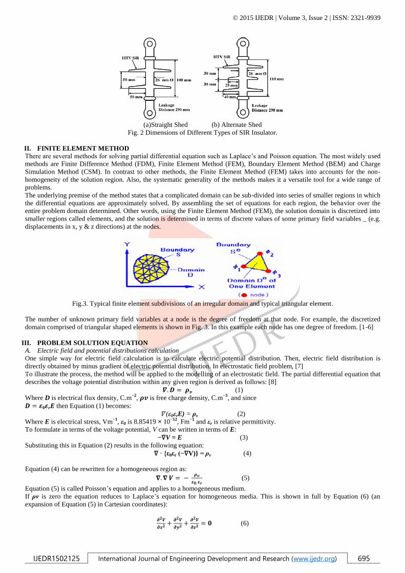
Two types of silicone rubber insulator are used: straight sheds with leakage distance 290 mm and alternate shed with leakage
distance 290 mm Fig.2. The 15 kV polymeric insulator models are simulated under clean, polluted surface conditions using
(FEM) Electrostatic Software.
© 2015 IJEDR | Volume 3, Issue 2 | ISSN: 2321-9939
IJEDR1502125 International Journal of Engineering Development and Research (www.ijedr.org) 695
(a)Straight Shed (b) Alternate Shed
Fig. 2 Dimensions of Different Types of SIR Insulator.
II. FINITE ELEMENT METHOD
There are several methods for solving partial differential equation such as Laplace’s and Poisson equation. The most widely used
methods are Finite Difference Method (FDM), Finite Element Method (FEM), Boundary Element Method (BEM) and Charge
Simulation Method (CSM). In contrast to other methods, the Finite Element Method (FEM) takes into accounts for the non-
homogeneity of the solution region. Also, the systematic generality of the methods makes it a versatile tool for a wide range of
problems.
The underlying premise of the method states that a complicated domain can be sub-divided into series of smaller regions in which
the differential equations are approximately solved. By assembling the set of equations for each region, the behavior over the
entire problem domain determined. Other words, using the Finite Element Method (FEM), the solution domain is discretized into
smaller regions called elements, and the solution is determined in terms of discrete values of some primary field variables _ (e.g.
displacements in x, y & z directions) at the nodes.
Fig.3. Typical finite element subdivisions of an irregular domain and typical triangular element.
The number of unknown primary field variables at a node is the degree of freedom at that node. For example, the discretized
domain comprised of triangular shaped elements is shown in Fig. 3. In this example each node has one degree of freedom. [1-6]
III. PROBLEM SOLUTION EQUATION
A. Electric field and potential distributions calculation
One simple way for electric field calculation is to calculate electric potential distribution. Then, electric field distribution is
directly obtained by minus gradient of electric potential distribution. In electrostatic field problem, [7]
To illustrate the process, the method will be applied to the modelling of an electrostatic field. The partial differential equation that
describes the voltage potential distribution within any given region is derived as follows: [8]
(1)
Where D is electrical flux density, C.m−2
, is free charge density, C.m−3
, and since
0 r then Equation (1) becomes:
∇ (ε0εrE) = ρv (2)
Where E is electrical stress, Vm−1
, ε0 is 8.85419 × 10⁻¹²
, Fm−1
and εr is relative permittivity.
To formulate in terms of the voltage potential, V can be written in terms of E:
−∇V = E (3)
Substituting this in Equation (2) results in the following equation:
∇ · ε0εr (−∇V) = ρv (4)
Equation (4) can be rewritten for a homogeneous region as:
(5)
Equation (5) is called Poisson’s equation and applies to a homogeneous medium.
If ρv is zero the equation reduces to Laplace’s equation for homogeneous media. This is shown in full by Equation (6) (an
expansion of Equation (5) in Cartesian coordinates):
(6)

© 2015 IJEDR | Volume 3, Issue 2 | ISSN: 2321-9939
IJEDR1502125 International Journal of Engineering Development and Research (www.ijedr.org) 696
Equation (6) is the partial differential equation that describes the voltage potential distribution in high voltage situations where the
medium is homogeneous and the charge density is zero. If the medium is non-homogeneous then Equation (6) is written as:
(7)
For each region. This is to allow for the different permittivities in the different regions.
To use Equation (7) in a finite-element formulation requires the equation to be transformed into an energy functional form that
relates directly to the electrical energy of the system. [8]
B. The energy functional illustrated
The total electrical energy in a system of volume Ω may be written as:
1.
2F D Ed
(8)
i.e.
2
0
1
2rF E d
(9)
If it is assumed that the permittivity is constant within the region concerned, then Equation (9) may be used to write the energy (in
a Cartesian coordinate system) as:
2 22
0 .2
r V V VF dxdydz
x y y
(10)
It can be shown that this is the functional that, when differentiated with respect to V and equated to zero, gives a distribution of V
that satisfies the governing partial differential equation. Physically, the process corresponds to minimizing the stored electrical
energy i.e. the potential energy of the system for the imposed boundary conditions. The differentiation is most conveniently
carried out on the discretized system.
For element e
2 22
0
2
re
e
V V VF dxdydz
x y y
(11)
Where suffix e indicates integration over an element. Hence, the contribution to the rate of change of F with V from the variation
of potential of node i in element e only, χe, is:
2 22
0
2
ee
i
r
ie
Fx
V
V V Vdxdy
V x y y
(12)
0
2 .
2 .2
2 .
i
re
ie
i
V V
x V x
V Vx dxdydz
y V y
V V
z V z
(13)
C. Numerical representation
To solve high voltage problems using the finite-element method requires Equation (13) to be equated to zero. To represent the
problem numerically, the problem region is divided into elements and Equation (13) is applied at the nodes forming the element
vertices. The variation of the potential over the elemental shape has then to be approximated by a polynomial distribution (known
as the shape function). The order of the chosen polynomial will dictate the type of element used, for example a linear distribution
would only require a simple triangular element. For higher order shape functions, the number of nodes describing the element

© 2015 IJEDR | Volume 3, Issue 2 | ISSN: 2321-9939
IJEDR1502125 International Journal of Engineering Development and Research (www.ijedr.org) 697
must be capable of defining the order used, e.g. a quadratic shape function over a triangular element requires nodes at the middle
of each element side. [8]
Fig.4. Elements associated with node i.
There will be contributions to the rate of change of the region functional χ with respect to the potential Vi at node i from all the
elements connected to i. In the case shown in Figure 4, there will be contributions from elements 1 to 6.
Hence, generally, the contribution to ∂F/∂V from a change in Vi is:
e
ei i
FF
V V
(14)
Where ∑e represents the summation of contributions from all elements associated with Vi, i.e., all the elements connected to
node i.
When these derivatives are equated to zero, a group of simultaneous equations is formed. These can be written in matrix form as:
0t iS V (15)
Where [St ] is a square matrix known as the stiffness matrix and is formed from the geometric coordinates of the nodes defining
the elements and the material properties.
Vi is a column matrix containing all the nodal potentials. The coefficient stiffness matrix will be sparse, i.e. it will contain many
zeros since, from the discussion above,
IV. FEM MODEL FOR TWO TYPES POLYMERIC INSULATOR
Two models of polymer insulator, "Straight Shed and Alternate Shed" was selected to simulate electric field and potential
distributions in this study. The basic three dimensions design of a polymer insulator is as follows; a fiber reinforced plastic (FRP)
core having relative dielectric constant of 7.1, attached with two metal fittings, is used as the load bearing structure. Weather
sheds made of high temperature vulcanized silicone rubber (HTV SiR) having relative dielectric constant of 4.3 are installed
outside the FRP core. Surrounding of the insulator is air having relative dielectric constant 1.0. A 15 kV voltage source directly
applies to the lower electrode while the upper electrode connected to ground. [9]. Three dimensions models of the two type
polymer insulators for FEM analysis are shown in fig (5).
(a)Straight Shed (b) Alternate Shed
Fig. 5 Three dimension models of the two type polymer insulators for FEM analysis.
This paper investigates the Electric field, and voltage distribution of the 15 kV polymeric insulators at two different surface
conditions such as:
Case 1: Dry and clean insulator.
Case 2: Non-uniform pollution layer, and Water droplets on the insulator surface.

© 2015 IJEDR | Volume 3, Issue 2 | ISSN: 2321-9939
IJEDR1502125 International Journal of Engineering Development and Research (www.ijedr.org) 698
Properties SI
R
FR
P
cor
e
Pollutio
n layer
Water
drople
t
Ai
r
Relative
Permittivity ɛ 4.3 7.1 8 81 1
Conductivity,
μs/cm 0 0 100 500 0
Thickness/Hei
ght - - 100µm 2mm -
Table 1. Material properties of FEM model
Tab. 1 shows the properties of the materials such as relative permittivity, conductivity and thickness/ height of pollution layer and
water droplets used for the FEM modeling of the insulators. The insulator is equipped with metal fittings at both line and ground
ends. [10]
Fig. 6 Finite element Mesh results.
The whole problem three-dimensional models in Fig. 5, and Air box surrounding is fictitiously divided into small triangular areas
called domain. The potential, which is unknown throughout the problem domain, is approximated in each of these elements in
terms of the potential in their vertices called nodes. The most common form of approximation solution for the voltage within an
element is a polynomial approximation.
The obtaining surface Mesh results are 5,287 nodes and 21,659 elements for straight sheds type insulator and 5,497 nodes and
22,302 elements for alternate sheds type insulator, respectively. The obtaining results are shown in Fig. 6.
V. RESULTS AND DISCUSSIONS
Clean and contamination conditions are simulated in this study. In case of contamination condition water droplets and non-
uniform pollution layer are placed on the two type insulator surfaces as shown in Fig.7.
(a)Alternate shed type pollution layer and meshing
(a). Straight Shed
5287 nodes and 21659
elements
(b). Alternate Shed
5497 nodes and 22302
elements

© 2015 IJEDR | Volume 3, Issue 2 | ISSN: 2321-9939
IJEDR1502125 International Journal of Engineering Development and Research (www.ijedr.org) 699
(b)Straight shed type pollution layer and meshing
Fig.7. Pollution layer and meshing for two type insulator
Potential and electric field distribution results for Alternate Sheds type under dry and clean conditions are shown in Fig. 8.
(a) Potential distribution
(b) Potential distribution lines (Insulator and Air box surrounding)
(c) Electric Field Distribution

© 2015 IJEDR | Volume 3, Issue 2 | ISSN: 2321-9939
IJEDR1502125 International Journal of Engineering Development and Research (www.ijedr.org) 700
(d) Electric Field Distribution lines (Insulator and Air box surrounding)
Fig. 8 Alternate Sheds Insulator Potential and Electrical field Distribution under Clean Condition.
Also electrical field along leakage distance of the insulator under dry and clean conditions are shown in Fig. 9.
Fig. 9 Electrical field along leakage distance for Alternate Sheds Insulator under Clean Condition.
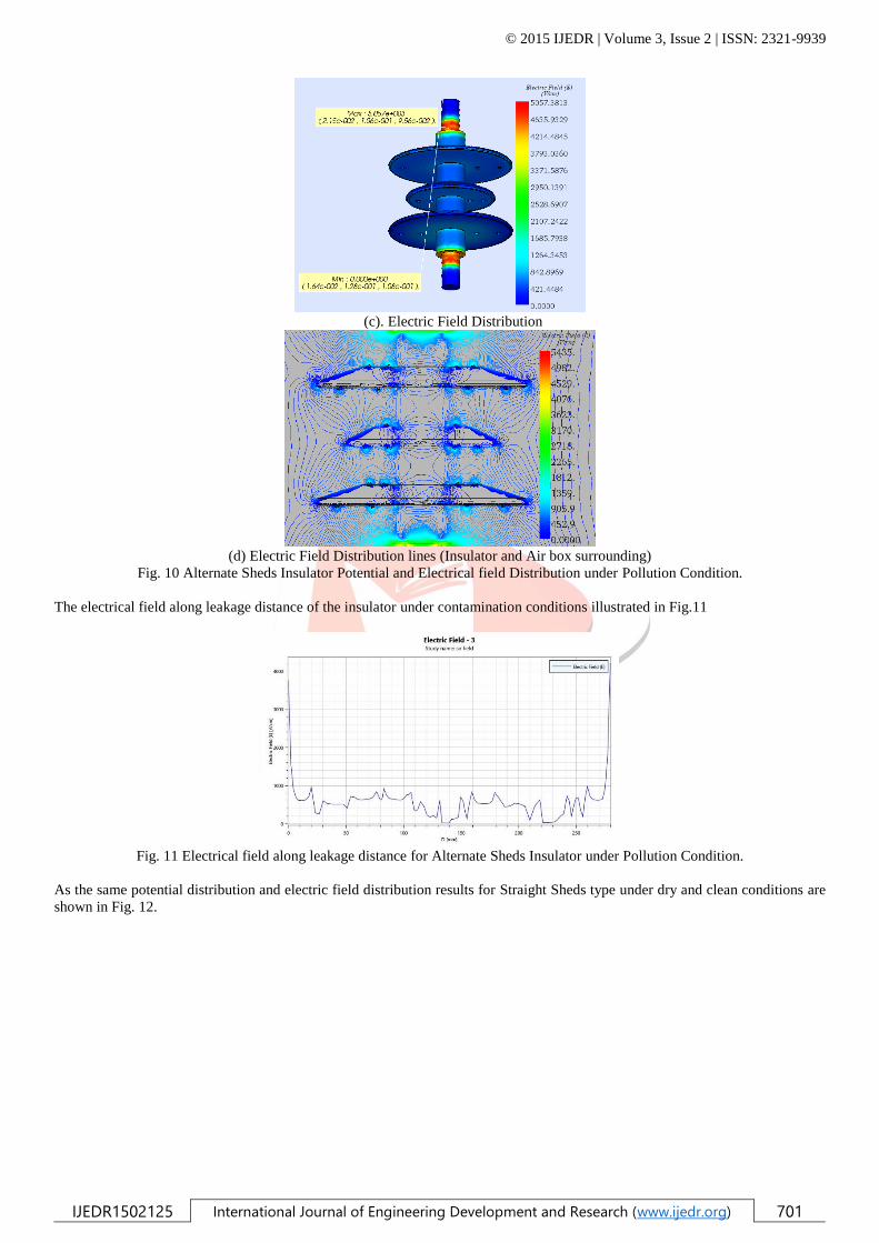
The potential and electric field distribution under pollution condition for the alternate shed type are illustrated in Fig.10.
(a) Potential distribution
(b) Potential distribution lines (Insulator and Air box surrounding)
© 2015 IJEDR | Volume 3, Issue 2 | ISSN: 2321-9939
IJEDR1502125 International Journal of Engineering Development and Research (www.ijedr.org) 701
(c). Electric Field Distribution
(d) Electric Field Distribution lines (Insulator and Air box surrounding)
Fig. 10 Alternate Sheds Insulator Potential and Electrical field Distribution under Pollution Condition.
The electrical field along leakage distance of the insulator under contamination conditions illustrated in Fig.11
Fig. 11 Electrical field along leakage distance for Alternate Sheds Insulator under Pollution Condition.
As the same potential distribution and electric field distribution results for Straight Sheds type under dry and clean conditions are
shown in Fig. 12.

© 2015 IJEDR | Volume 3, Issue 2 | ISSN: 2321-9939
IJEDR1502125 International Journal of Engineering Development and Research (www.ijedr.org) 702
(a) Potential distribution
(b) Potential distribution lines (Insulator and Air box surrounding)
(c). Electric Field Distribution
(d) Electric Field Distribution lines (Insulator and Air box surrounding)
Fig. 12 Straight Sheds Insulator Potential and Electrical Field Distribution under Clean Condition.
The electrical field along leakage distance of the insulator under dry and clean conditions are shown in Fig. 13.

© 2015 IJEDR | Volume 3, Issue 2 | ISSN: 2321-9939
IJEDR1502125 International Journal of Engineering Development and Research (www.ijedr.org) 703
Fig. 13 Electrical field along leakage distance for Straight Sheds Insulator under Clean Condition.
The potential and electric field distribution under pollution condition for the straight shed type are illustrated in Fig.14.
(a) Potential distribution
(b) Potential distribution lines (Insulator and Air box surrounding)
(c). Electric Field Distribution

© 2015 IJEDR | Volume 3, Issue 2 | ISSN: 2321-9939
IJEDR1502125 International Journal of Engineering Development and Research (www.ijedr.org) 704
(d) Electric Field Distribution lines (Insulator and Air box surrounding)
Fig. 14 Straight Sheds Insulator Potential and Electrical Field Distribution under Pollution Condition.
The electrical field along leakage distance of the insulator illustrated in Fig.15
Fig. 15 Electrical field along leakage distance for Straight Sheds Insulator under Pollution Condition.
Comparison results illustrated in Fig.9 and Fig.11, are shown that obvious difference in magnitude of electric field and
nonlinearity can be seen on the sheds of the alternate sheds insulator in case of contamination.
As the same, in the results illustrated in Fig.13 and Fig.15, shown that obvious difference in magnitude of electric field and
nonlinearity can be seen on the sheds of the straight sheds insulator in case of contamination.
In case of dry and clean conditions, comparison results illustrated in Fig.8 and Fig.12 shown that the electric field intensity on
Straight Sheds type (with maximum value
4207(V/cm)), is Higher than the electric field intensity on Alternate Sheds type (with maximum value 3986(V/cm)).
In case of contamination with water droplets conditions, comparison results illustrated in Fig.10 and Fig.14 shown that the electric
field intensity on Straight Sheds type (with maximum value 6666(V/cm)), is Higher than the electric field intensity on Alternate
Sheds type (with maximum value 0607(V/cm)).
Fig. 16 Comparison of Potential Distribution for two type insulator under clean condition
.

© 2015 IJEDR | Volume 3, Issue 2 | ISSN: 2321-9939
IJEDR1502125 International Journal of Engineering Development and Research (www.ijedr.org) 705
Fig. 17 Comparison of Potential Distribution for two type insulator under Pollution condition.
Comparison of potential distribution along leakage distance under clean and contamination condition for two type insulator is
illustrated in Fig.16 and Fig.17 respectively show that more nonlinear potential distribution obtained from the straight sheds
insulator comparing with the alternate sheds type.
VI. CONCLUSION
In many research, the potential and electric field distribution on high voltage polymer insulators has been estimated in two-
dimension models, but in this paper, a three-dimensional model used to study the same Insulators, and this gives a high accuracy
of the study results. The electric field and potential distributions on Straight sheds & Alternate shed silicone rubber polymer
insulators under clean and contamination conditions were investigated by using FEM. Higher magnitude of electric field
distribution and more nonlinear potential distributions on the straight sheds insulator comparing with the alternate shed type
obtained from the simulation results by using Finite Element Method. And it’s caused more electric discharge on the insulator
surface. More discharge activities caused severe surface damages and possible flashover within operating conditions.
VII. REFERENCE
[1] G. Satheesh, B. Basavaraja, Pradeep M. Nirgude, “Electric Potential Comparision along Surface of SiR Insulators Using
FEM”, The SEARCH Digital library, No.142, pp 684-689.
[2] B. Marungsri, “Fundamental Investigation on Salt Fog Ageing Test of Silicone Rubber Housing Materials for Outdoor
Polymer Insulators”, Doctoral Thesis, Chubu University, Kasugai, Aichi, Japan, 2006.
[3] B. Marungsri, W. Onchantuek, A. Oonsivilai, T. Kulworawanichpong, “Analysis of Electric Field and Potential
Distributions along Surface of Silicone Rubber Insulators under Various Contamination Conditions Using Finite Element
Method”, World Academy of Science, Engineering and Technology 53, 2009, pp 1353- 1363
[4] CIGRE TF33.04.07, “Natural and Artificial Ageing and Pollution Testing of Polymer Insulators”, CIGRE Pub. 142, June
1999.
[5] S. H. Kim, R. Hackam, “Influence of Multiple Insulator Rods on Potential and Electric Field Distributions at Their
Surface”, Int. Conf. on Electrical Insulation and Dielectric Phenomena 1994, October 1994, pp. 663 – 668.
[6] G. Satheesh, B. Basavaraja, Pradeep M. Nirgude, “Electric Field along Surface of Silicone Rubber Insulator under Various
Contamination Conditions Using FEM”, International Journal of Scientific & Engineering Research, Volume 3, Issue 5,
May-2012
[7] S. Sangkhasaad, “High Voltage Engineering”, 3td edition, Printed in Bangkok, Thailand, March 2006 (in Thai).
[8] A. Haddad, D.F.Warne, “Advances in High Voltage Engineering” ,1st edition, and Reprinted 2007, Published by The
Institution of Engineering and Technology, London, United Kingdom, 2007.
[9] Vishal Kahar, Ch.v.sivakumar, .Basavaraja.B, “Finite Element Analysis on Post Type Silicon Rubber Insulator Using
MATLAB” International Journal of Engineering Development and Research, , National Conference (RTEECE-2014) -17th
,18th January 2014, pp 23-28
[10] Chinnusamy Muniraj, Subramaniam Chandrasekar, “Finite Element Modeling for Electric Field and Voltage Distribution
along the Polluted Polymeric Insulator”, World Journal of Modelling and Simulation Vol. 8 (2012) No. 4, pp. 310-320,
ISSN 1 746-7233, England, UK
[11] v.sivakumar, .Basavaraja.B, “Design and Evaluation of Different Types of Insulators Using PDE Tool Box”, International
Conference on Computing, Electronics and Electrical Technologies, 2012, pp 332-337
[12] B. Marungsri, W. Onchantuek, and A. Oonsivilai, “Electric Field and Potential Distributions along Surface of Silicone
Rubber Polymer Insulators Using Finite Element Method”, World Academy of Science, Engineering and Technology 42
2008, pp 67-72
[13] Boonruang Marungsri, Hiroyuki Shinokubo, Ryosuke Matsuoka, “Effect of Specimen Configuration on Deterioration of
Silicone Rubber for Polymer Insulators in Salt Fog Ageing Test” IEEE Transactions on Dielectrics and Electrical
Insulation Vol. 13, No. 1; February 2006, pp 129-138