etching of - nasa · dry etching of metallizations david bollinger ... and/or copper (up to 4%) and...
TRANSCRIPT

DRY ETCHING OF METALLIZATIONS
DAVID BOLLINGER
VEECO INSTRUHENT!3
PLAINVIEW, NEW YORK
The production dry e t ch processes from t h e perspect ive of microelectronic fabr ica t ion appl ica t ions are reviewed. While f o r semiconductors, t h e t e r m "metallitat ion" is generalized to include a l l conductors, p a r t i c u l a r l y doped polysi l icon, t h e only actual metals extensively used in t h e l a rge volume semiconductor appl ica t ions are aluminum based. t i ons is fn the form of an a l l o y with s i l i c o n (usual ly 1%) and/or copper (up t o 4%) and sometimes i n conjunction with a barrier metal such as t i tanium t o prevent d i f fus ion of s i l i con . retals has been concentrated on developing r e l i a b l e production processes f o r t he aluminum based meta l l iza t ions . And, only within t h e pas t two years, has dry etching of aluminum emerged from the laboratory i n t o production, primar- i l y because of progress i n Reactive Ion Etch mode p l a s m systems, (discussed below) along with t h e associated gas chemistries.
A l u m i n u m in these appl ica-
Consequently, recent work in dry etching of
For d ry etching, appl ica t ions are t o t h i n f i lms with thicknesses usua l ly Dry less than 2 microns and with a pa t t e rn defined by a photo resist mask.
etching provides the advantages of (1) el iminat ing d i sposa l of hazardous chemicals, (2) etching materials that are d i f f i c u l t t o w e t e tch, and (3) etching pa t t e rns with v e r t i c a l walls, t h a t 'is, etching an iso t ropica l ly . Anis- ot ropic e tching is esse.tia1 t o advanced microelectronic devices because: (a) underci-L lh i ts l i n e width sites and corresponding "packing density", (b) l o s s of cross-sect ional area of a conductor causes increased res i s tance , and (c) a negative s lope type undercut, as tends to occur i f aluminum etching is not f u l l y an iso t ropic , makes s t e p coverage by a subsequent l aye r d i f f i c u l t . For a dry etch appl icat ion, e tch qua l i t y criteria which should be considered are: the degree of anisotropy, e tch s e l e c t i v i t y (with respec t t o mask and undeilying l aye r ) , e tch uniformity, res idue a f t e r e tch ing (compare f i g u r e s 1 and 2) corrosion a f t e r e tching (a c r i t i c a l considerat ion with aluminum), thruput requirements, and process r e l i a b i l i t y .
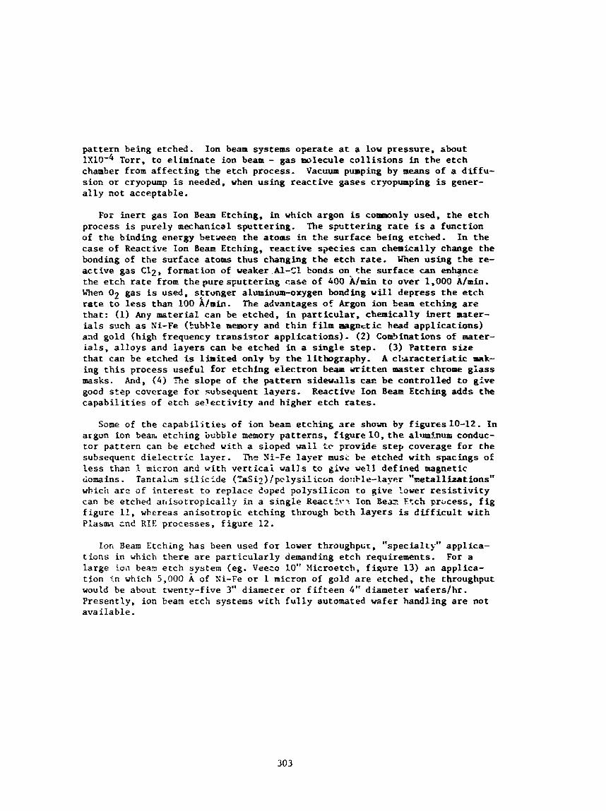
The major dry e tch processes used i n t h e f ab r i ca t ion of microelectronic devices. given i n f igu re 3, can be divided i n t c two ca t egor i e s - Plasma pro- cesses in which samples are d i r e c t l y exposed t o an electrical discharge, and f m Beam processes i n which samples are etched by a bean; of ions extracted fr,m a discharge. The plasma e tch processes san be dis t ingutshed by the de- gree t o which ion bombardment cont r ibu tes t o t h e e t ch process. is re la ted t o capab i l i t y f o r an iso t ropic etching. and Ion Beam Etching are of most i n t e r e s t f o r e tching of t h i n f i lm metals. R I E is general ly considered the best process f o r l a r g e volume, an iso t ropic aluminu*J etching.
This, In tu rn Reactive Ion Etching (RIE)
Barrel Type Plaslne Etchers
The Barrel Type plasma e tch configuratlon, schi I f , :kte 4, is usua l ly
30 1
https://ntrs.nasa.gov/search.jsp?R=19840013929 2018-07-16T15:06:54+00:00Z

a quar tz c y l i n d e r i n t o which wafers are loaded concent r ic t o t h e c y l i n d e r a x i s . An RF discharge, with f i e l d s appl ied e x t e r n a l t o t h e r e a c t o r vessel, fragments t h e gas i n t o chemically r e a c t i v e spec ies . A s h i e l d i n g screen may be used tc prevent t h e ionized gas from reaching t h e wafers. Etching is then pr imari ly , or e n t i r e l y , hy n e u t r a l , chemically reactive spec ies . The advan- tages of b a r r e l type r e a c t o r s are t h e i r high throughput a t a low c a p i t a l cos t . The disadvantages are that e tch ing i s pure ly chemical, and cherefore i s o t r o p i c , and t h a t materials f o r which bombardment is needed t o c o n t r i b u t e t o t h e e t c h process (eg. Si021 are d i f f i c u l t t o e t c h .
Plasma Mode and R I E Mode Plasma Systems
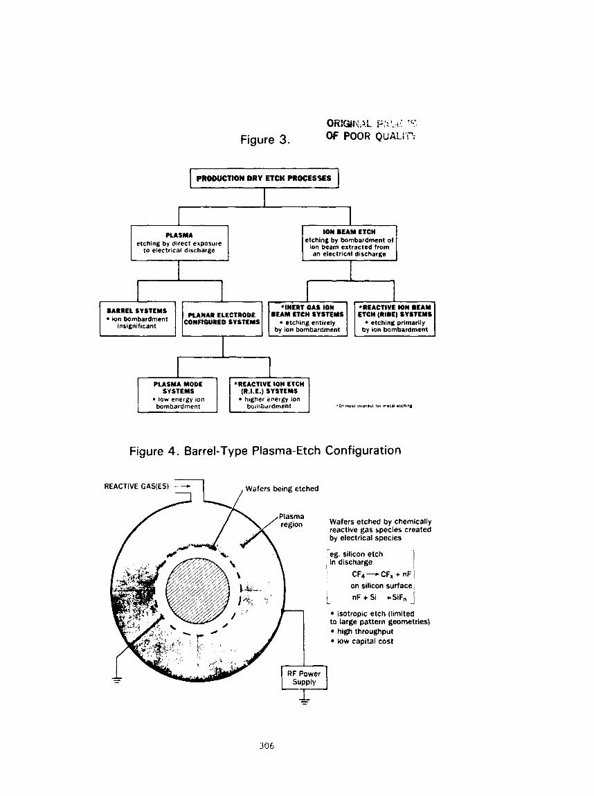
Plasma Mode and R I E Mode p lanar e l e c t r o d e conf igura t ions , f i g u r e s 5 and 6 , have two important d i f f e r e n c e s : (1) RIE o p e r a t e s a t a lower p r e s s u r e (L200 microns), and (2) f o r R I E , t h e wafers sit on a c a p a c i t i v e l y coupled, RF dr iven e lec t rode , while for t h e plasma mode, wafers are on a grounded elec- t rode. I n t h e R I E mode, wafers being etched can take on a n average negat ive s e l f b i a s v o l t a g e with r e s p e c t t o t h e plasma and, as a r e s u l t , e n e r g e t i c ion bombardment ( i n t h e range of several hundred e V as opposed t o less than 50 eV f o r P l a s m mode opera t ion) can c o n t r i b u t e t o t h e e t c h process . The e n e r g e t i c ion bombardment provides t h e R I E process wi th its a n i s o t r o p i c e t c h c a p a b i l i t - ies ( f i g u r e 7) . Anisotropic e t c h i n g is p o s s i b l e i n t h e Plasma mode but such processes are much more dependent on polymerization processes t o p r o t e c t t h e p a t t e r n s idewal l from undercut than i n R I E processes .
As with t h e b a r r e l e t c h process , i n Plasma mode and R I E chemical ly re- a c t i v e s p e c i e s are created by t h e RF discharge. However, e t c h mechanisms, and hence e t c h c h a r a c t e r i s t i c s , d i f f e r as a r e s u l t of t h e degree of ion bom- bardment. I n R I E processes f o r Aluminum, t h e chemically reactive s p e c i e s are c h l o r i n e s p e c i e s produced 5y fragmentation of molecules conta in ing ch lor - ine ( i e . B C l 3 , C C l 4 , C 1 2 , S i C 1 4 ) . The s u r f a c e s which are etched, those par- a l l e l t o t h e e l e c t r o d e t o which t h e wafers a r e a f f i x e d , cont inuously andergo ion bombardment which c l e a n s t h e s u r f a c e of n a t i v e oxide, o r any o t h e r re- a c t i o n i n h i b i t i n g l a y z r ( f i g u r e 7 ) . D i r e c t i o n a l e t c h i n g can then proceed by the r e a c t i v e c h l o r i n e s p e c i e s forming aluminum c h l o r i d e s which, having a low vapor pressure , can lx puqped away.
Ful ly automated, casse t te - to-casse t te , load locked Plasma and RIE mode systems are a v a i l a b l e . a t i n g pressure can have much higher etch rates, thus s i n g l e wafer a t a time as w e l l a s batch systems are made. to -casse t te , load locked R I E system f o r l a r g e volume aluminum, S i 0 2 and poly- s il icon e tch ing .
Plasma mode systems, by v i r t u e of t h e i r h igher oper-
Figure 8 shows t h e Veeco DV-40 cassette-
Ion Beam and Reactive Lon Beam Etching
Ion beam e tch ing is accomplished by a col l imated beam of ions which is ex- t rac ted from a d ischarge by a set of g r i d s ( f i g u r e 9) . etched a r e a f f i x e d t o a t a r g e t p l a t e which must preform t h e m u l t i p l e func- t ims of : (i) heat s ink ing t h e wafers being etched t o prwent overheat ing, p a r t i c u l a r l y of resist, ( 2 ) t i l t a t an angle wi th r e s p e c t t o t h e i c c i d e n t ion beam t o give c o n t r o l over t h e p s t t e r n s idewal l characteristics, and (3) r o t a t e i n t h e ion beam t o symmetrically average t h e a f f e c t of t h e t i l t on t h e
S u b s t r a t e s t o be
302
p a t t e r n being etched. Ion beam systems o p e r a t e a t a l o w pressure , about lX10-4 Torr, t o eliminate ion beam - gas molecule c o l l i s i o n s in t h e e t c h chamber from a f f e c t i n g t h e e t c h process. s ion or cryopump is needed, when us ing r e a c t i v e gases cryopumping is gener- a l l y not acceptable .
Vacuum pumping by m e a n s of a d i f f u -
For i n e r t gas Ion Beam Etching, in uhich argon is corPnronly used, t h e e t c h process i s purely mechanical s p u t t e r i n g . of t h e binding energy bet;reer? t h e atoms i n t h e s u r f a c e Seing etched. I n t h e case of Reactive Ion Beam Etching, r e a c t i v e s p e c i e s can chemically change t h e bonding of t h e s u r f a c e atoms t h u s changing t h e e t c h rate. men us ing t h e re- a c t i v e gas C12, formation of weaker Al-SI bonds on t h e s u r f a c e can enhqnce t h e e t c h rate from t h e pure s p u t t e r i n g case of 600 Afmin to over 1,000 A/min. When 02 gas is used, sFronger aluminum-oxygen boding w i l l depress t h e e t c h rate to less than 100 A f m i n . t h a t : (1) Any nuterial can be etched, i n p a r t i c u l a r , chemically i n e r t aater- ials silch as Si-Fe (bubble memory and t h i n f i l m e a g n e t i c head a p p l i c a t i o n s ) a3d gold (high frequency t r a n s L s t o r a p p l i c a t i o n s ) - (2) Cowbinations of mater- ia ls , a l l o y s and i a y e r s can be etched i n a s i n g l e s t e p . (3) P a t t e r n s i z e t h a t can be etched is limited only by t h e l i thography. A clsracteristic mak- ing t h i s process usefu l for e tch ing e l e c t r o n beam i r r i t t e n master chrome g i a s s masks. And, (4) The s lope of t h e p a t t e r n sidewalls can be c o n t r o l l e d to g2ve goad S%Q coverage f o r subsequent layers . Reactive Ion Be- Etching adds t h e c a p a b i l i t i e s of e t c h se! e c t i v i t y and h igher e t c h rates.
The s p u t t e r i n g rate is a funct ion
The advantages of Argon ion beam e tch ing are
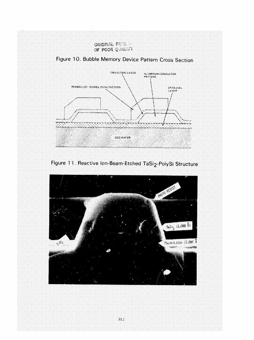
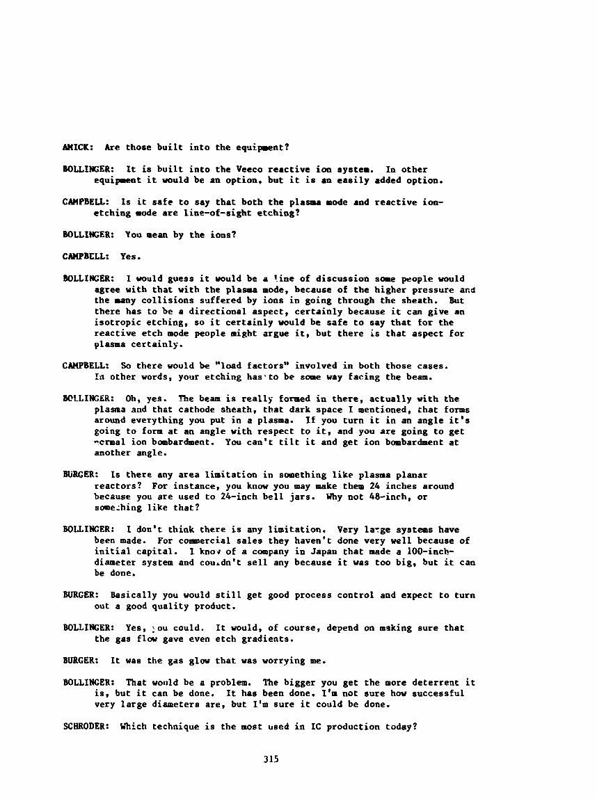
Some of t h e c a p a b i l i t i e s of ion bean e tch ing are shoun by f i g u r r s l 0 - 1 2 . In argon ion bean. e tch ing bobble memory p a t t e r n s , f i g u r e l 0 , t h e aluminum conduc- t o r p a t t e r n can be etched with a sioped wal l 'cc provide s t e p coverage f o r t h e subsequent d i e l e c t r i c layer . The Si-Fe l a y e r musi be etched wi th spacings of less thar. 1 micron and with v e r t i c a l w a l l s to give vel1 defined magnetic tioma i n s . T a n t a l m si1 i c ;de (TaS i 2 ) !pclysi l icrin dio::i-le-laser "metaflizat ions" which aro, of i n t e r e s t t o rep lace Coped p o l y s i l i c o n t a give lower r e s i s t i v i t y can be etched a n i s o t r o p i c a l l y in a s i n g l e React:\-- Ian Becrz Ftch pri)cess, f i g f i g u r e 11, whereas a n i s o t r o p i c e tch ing through bc th l a y e r s is d i f f i c u l t wi th Plasm? a d RIE processes , f i g u r e 12.
Iofi Beam Etching has been used f o r lower throughptic, "special ty" appl ica- t i o n s in which t h e r e are p a r t i c u l a r l y demanding e t c h requirements. l a r g e ioai bean e t c h system (eg. Veeco LO" Nicroetch, f i g u r e 13) an appl ica- t ion i n which 5,000 A of Si-Fe or 1 micron of gold are etched, t h e throughput would be about twenty-five 3" diameter or f i f t e e n 4" diameter wafersfhr . Present ly , ion beam etch systems with f u l l y automated wafer handl ing are not a v a i l a b l e .
For a
303


W N A L P A G :j PO9R QLJALiTY
Figure 2. Plasma-Etched Patte. n With Residue
f t l ;
PRODUCTION DRY ETCK PROCESSES
I
. BARREL
ion bombardment insignificant
PLASMA etching by direct eiposure
to electrical discharge
.INERT CAS ION *REACTIVE ION BEAM PLANAR ELECTRODE 'BEAM ETCH SYSTEMS ETCH (RIBE) SYSTEMS
by ion bombardment CONFIGURED SYSTEMS etching entirely etching primarily
by ion bombardment
ION BEAM ETCH I I etching by bombardment of
ion beam extracted from an electrical discharee
(R.I.E.) SYSTEMS higher ebergy ion bombardment .ot most ,nter..t IO, metal .tcni*a
PLASMA MODE SYSTEMS
low energy ion ' bombardment
Figure 4. Barrel-Type Plasma-Etch Configuration
Wafers being etched / REACTIVE GAS(ES) -4
Plasma / region Wafers etched by chemically reactive gas species created by electrical species
eg. silicon etch in discharge
CF4 - CF, + nF on silicon surface
I nF + Si -SiFn L
isotropic etch (limited to large pattern geometries)
high throughput low capital cost
306

Figure 5. Plasma Mode Type Etch System
DRIVEN ELECTRODE
PLASMA
WAFERS
\VARIABLE CONDUCTANCE VALVE
GAS EXHAUST (PUMPING SYSTEM)
307

Figure 6. Reactive Ion Etch Chamber
GAS EXHAUST (PUMPING SYSTEM)
30 8
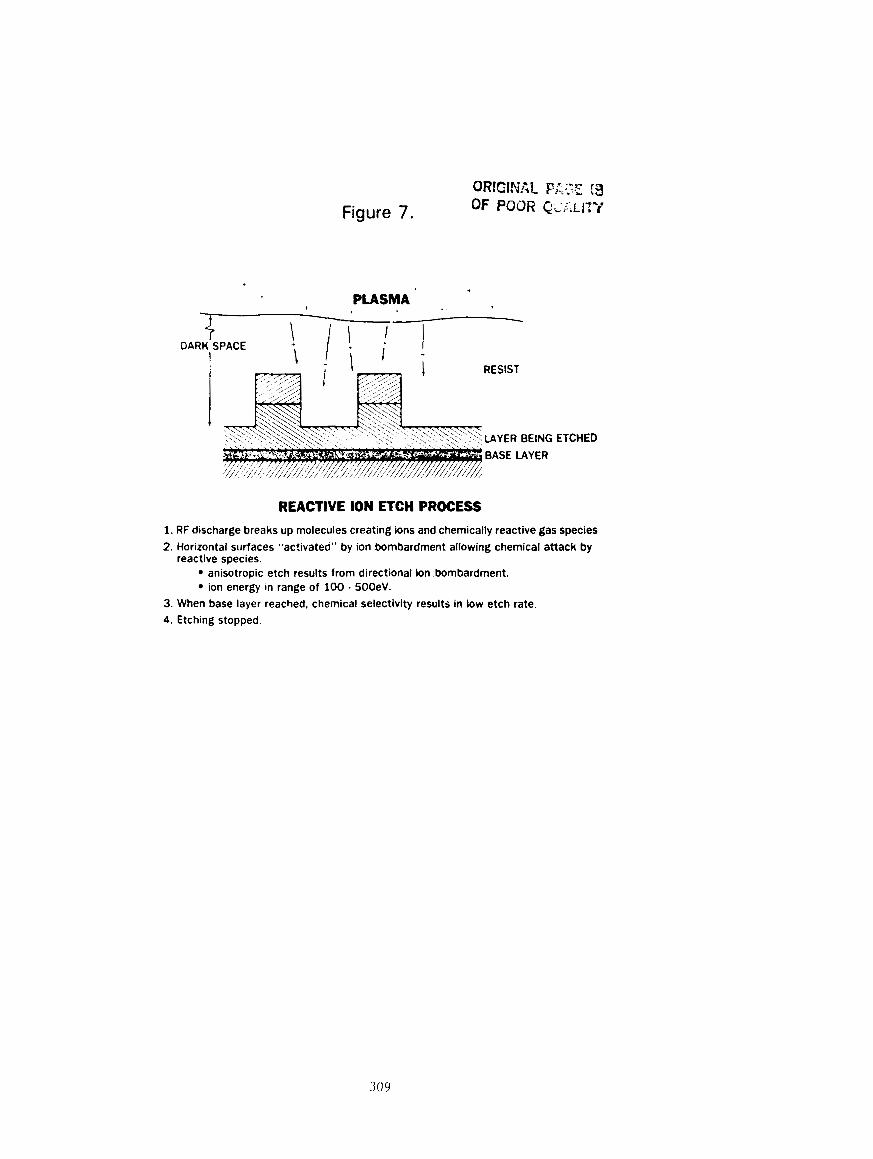
Figure 7.
t
PLASMA - -+ DARK SPACE
LAYER BEING ETCHED
REACTIVE ION ETCH PROCESS 1. RF discharge breaks up molecules creating ions and chemically reactive gas species 2. Horizontal surfaces "activated" by ion bombardment allowing chemical attack by
reactive species. anisotropic etch results from directional ion .bombardment. ion energy in range of 100 - 500eV.
3. When base layer reached, chemical selectivity results in low etch rate. 4. Etching stopped.

Figure 9. Production Ion Milling System
NEUTRAL 12 AT ION FILAMENT
OPT1 CALLY A LlONCO QRID3 TO EXTRACT WIQHLY COLLIMATED. @LAY
TAROCT CHAMBER FIX TUR I NO
FIXTURINQ MSLKATC MUST GIVE EASY ACCESS TO ALLOW RAPID LOADINO AND UNLOADINO
’
- - e a e
0-0 0 0
0 0-00
ION BEAM PLASMA COMPLETELY CONFINED TO DISCHARGE
TARGET PLATE REQUIRED TO: SOURCE CHAMBER POSITION SAMPLES MAINTAIN SAMPLES AT LOW TEMPERATURE A S SHOWN HERE SOLENOID COIL PROVIDES TILT TO SET ANGLE OF BEAM INCIDENCE MAGNETIC FIELD F O R CONFINEMENT OF ROTATE DURING MILLING ELECTRONS E M I T T E D FROM CATHODE
0 ION 0 ELECTRON


DISCUSS ION
GALLAGHER: Have you, in your travels, ever done any etching using shaped electrodes, to givr yo19 patterns wiLhout using photolithographic processes? For example, in our system, which you may or may not be familiar with, we had one of our contractors etch silicon nitride, were using silicon nitride basically as an AR coating i n this application and he wanted to make rather gross patterns, in relation to what you are doing, through the silicon nitride at the top of the solar cell, BO that he co'ild later plate contacts down in there and make his top contact. corner.
We
The gentleman who did some of it is sitting over in the I just wondered if you had any history or knowledge of it.
BOLLINGER: Veeco hasn't done any direct etching without masking. We haven't done any specifically that I'm aware of. and single-ion-bfam etching were done throuei:. a mask, but not on a wafer directly.
Both direct-writing etching
GALLAGHER: Bob (Pryor), can you tell us a little bit about the conclusions Motorola reached on that?
PRYOR: We've used brtsicalLy '.he parallel-plate type of method i.n the reactive ion mode, with a mechanical mask to actually shadow the impinging beam and etch where you want to etch without applying photoresist or any other kind of resist. That was tSe process developed on one of the former JPL contracts that we had. quite well down to things on the order of about 1 mil in terms of ?;ne widths, which for out application is the size we were interested in.
It works very successfully and worked'
BOLLINGER: Do you use a plate or something to shadow?
PRYOR: Yes, in effect, to put a shadow plate with a grid pattern in between the plasma and the substrate. It masks the accelerated ions and it works quite well,
AMICK: Can you say whether it is possible to monitor ;he progress of the etching by looking at the plpsma emission?
BOLLINGER: Oh, yes. For plasma processes, a very good diagnostic tool, as wel.1 as for detecting end point, is optical emission spectroscopy, because you can look at a line, such as when etching aluminum or monatomic excitation lines. basically proportional to the etch rate.
And the amount of the light emitted is
AMICK: Have you worked out sny reactive ion etching techniques for diapqostic purposes using plasma emission?
BOLLINGER: Oh, yes. It is used in those techniques; in a reactive ion technique it works vary well. Aluminum works very well; it's particularly good. In etching silicon dioxide you usually monitor the carbon monoxide line, which is not quite as good as the aluminum line, but those are very good diagnostic techniques for doing etching as well as monitoring end point.
314
AnICK: Are those b u i l t i n t o the equipment?
BOUINGER: It is b u i l t i n t o the Veeco r eac t ive ion system. In o ther equipment it vould be an option, but i t is an e a s i l y added option.
CAMPBELL: Is it s a f e t o say tha t both the plasma mode and r eac t ive ion- e tch ing mode are line-of-sight e tching?
BOUIHCER: You mean by the ions?
CAMPBELL: Yes.
BOLLINGER: I vould guess i t would be a 1.ine of d i scuss ion same people would agree with t h a t with the plasma mode, because of the higher pressure and the many c o l l i s i o n s suffered by ions i n going through the sheath. But there has t o be a d i r ec t iona l aspect , c e r t a i n l y because it can give an i so t rop ic etching, so i t c e r t a i n l y would be s a f e t o say that for the r eac t ive etch mode people might argue it , but there is t h a t aspect for plasma cer ta in ly .
CAMPBELL: So there would be "load factors" involved i n both those cases. In other words, your e tching h a s - t o be some way fac ing the beam.
BCLLINGER: Oh, yes. The beam is really formed i n there , ac tua l ly with the plasma and tha t cathode sheath, t ha t dark space I mentioned, chat forms around everything you put i n a plasma. If you turn it i n an angle it 's going t o form at an angle with respec t t o i t , and you are going t o get -crmal ion bombardment. another angle.
You can ' t t i l t it and ge t ion bombardment a t
BURGER: Is there any area l imi t a t ion i n something l i k e plasma planar
Why not 48-inch, or reac tors? because you are used t o 24-inch b e l l jars. some:hing l i k e tha t ?
For instance, you know you may make them 24 inches around
BOLLINGER: I don't think there is any l imi ta t ion . Very l a t g e s y s t m s have been made. i n i t i a l cap i t a l . diameter sys tem and couldn't se l l any because i t was too big, but it can be done.
For commercial sales they haven't done very w e l l because of I knog of a company i n Japan t h a t made a 100-inch-
BURGER: Basically you would s t i l l get good process cont ro l and expect t o turn out a good qua l i ty product.
BOLLINGER: Yes, lou could. It would, of course, depend on making s u r e t ha t the gas f l w gave even etch gradients ,
BURGER: It was the gas glw t h a t was worrying me.
BOLLINGER: That would be a problem. The bigger you get t he more de te r ren t i t is, but i t can be done. It has been done. I'm not sure how successful very l a rge diemeters are , but I'm sure i t could be done.
SCHRODER: Which technique i s the most used i n I C production today?
315

BOLLINCER: If you just say silicon device production, it depends on the If you don't worry about anisotropic, certainly the barrel size.
reactors are the most comonly used today. microns and in that range, but for the newer devices, so-called VISI (Very-Large-Scale Integration), reactive ion etch and plasma mode are used almost exclusively.
Host of IC production is 5
SCHRODER: Ion beam is hardly used for the large application, Is that right?
BOLLINCER: For the large-throughput applications, ion beam just doesn't have the throughput, end the plasma aode and the RE lode systas can handle the semiconductor materials vell, so ion-beam equipment has not been developed for high throughput at this tire.
316