evaluating phase change memory for enterprise · pdf fileevaluating phase change memory for...
TRANSCRIPT
This paper is included in the Proceedings of the 12th USENIX Conference on File and Storage Technologies (FAST ’14).
February 17–20, 2014 • Santa Clara, CA USA
ISBN 978-1-931971-08-9
Open access to the Proceedings of the 12th USENIX Conference on File and Storage
Technologies (FAST ’14) is sponsored by
Evaluating Phase Change Memory for Enterprise Storage Systems: A Study of Caching
and Tiering ApproachesHyojun Kim, Sangeetha Seshadri, Clement L. Dickey, and Lawrence Chiu,
IBM Almaden Research Center
https://www.usenix.org/conference/fast14/technical-sessions/presentation/kim

USENIX Association 12th USENIX Conference on File and Storage Technologies 33
Evaluating Phase Change Memory for Enterprise Storage Systems:A Study of Caching and Tiering Approaches
Hyojun Kim, Sangeetha Seshadri, Clement L. Dickey, Lawrence ChiuIBM Almaden Research
Abstract
Storage systems based on Phase Change Memory (PCM)devices are beginning to generate considerable attentionin both industry and academic communities. But whetherthe technology in its current state will be a commerciallyand technically viable alternative to entrenched technolo-gies such as flash-based SSDs remains undecided. To ad-dress this it is important to consider PCM SSD devicesnot just from a device standpoint, but also from a holisticperspective.
This paper presents the results of our performancestudy of a recent all-PCM SSD prototype. The aver-age latency for a 4 KiB random read is 6.7 µs, whichis about 16× faster than a comparable eMLC flash SSD.The distribution of I/O response times is also much nar-rower than flash SSD for both reads and writes. Based onthe performance measurements and real-world workloadtraces, we explore two typical storage use-cases: tier-ing and caching. For tiering, we model a hypotheticalstorage system that consists of flash, HDD, and PCM toidentify the combinations of device types that offer thebest performance within cost constraints. For caching,we study whether PCM can improve performance com-pared to flash in terms of aggregate I/O time and readlatency. We report that the IOPS/$ of a tiered storagesystem can be improved by 12–66% and the aggregateelapsed time of a server-side caching solution can be im-proved by up to 35% by adding PCM.
Our results show that – even at current price points –PCM storage devices show promising performance as anew component in enterprise storage systems.
1 Introduction
In the last decade, solid-state storage technology hasdramatically changed the architecture of enterprise stor-age systems. Flash memory based solid state drives(SSDs) outperform hard disk drives (HDDs) along a
number of dimensions. When compared to HDDs, SSDshave higher storage density, lower power consumption, asmaller thermal footprint and orders of magnitude lowerlatency. Flash storage has been deployed at various lev-els in enterprise storage architecture ranging from a stor-age tier in a multi-tiered environment (e.g., IBM EasyTier [15], EMC FAST [9]) to a caching layer withinthe storage server (e.g., IBM XIV SSD cache [17]), toan application server-side cache (e.g., IBM Easy TierServer [16], EMC XtreamSW Cache [10], NetApp FlashAccel [24], FusionIO ioTurbine [11]). More recently,several all-flash storage systems that completely elimi-nate HDDs (e.g., IBM FlashSystem 820 [14], Pure Stor-age [25]) have also been developed. However, flashmemory based SSDs come with their own set of concernssuch as durability and high-latency erase operations.
Several non-volatile memory technologies are beingconsidered as successors to flash. Magneto-resistiveRandom Access Memory (MRAM [2]) promises evenlower latency than DRAM, but it requires improvementsto solve its density issues; the current MRAM designs donot come close to flash in terms of cell size. FerroelectricRandom Access Memory (FeRAM [13]) also promisesbetter performance characteristics than flash, but lowerstorage density, capacity limitations, and higher costissues remain to be addressed. On the other hand,Phase Change Memory (PCM [29]) is a more immi-nent technology that has reached a level of maturity thatpermits deployment at commercial scale. Micron an-nounced mass production of a 128 Mbit PCM device in2008 while Samsung announced the mass production of512 Mbit PCM device follow-on in 2009. In 2012, Mi-cron also announced in volume production of a 1 GbitPCM device.
PCM technology stores data bits by alternating thephase of material between crystalline and amorphous.The crystalline state represents a logical 1 while theamorphous state represents a logical 0. The phase is al-ternated by applying varying length current pulses de-

34 12th USENIX Conference on File and Storage Technologies USENIX Association
pending upon the phase to be achieved, representingthe write operation. Read operations involve applyinga small current and measuring the resistance of the ma-terial.
Flash and DRAM technologies represent data by stor-ing electric charge. Hence these technologies have dif-ficulty scaling down to thinner manufacturing processes,which may result in bit errors. On the other hand, PCMtechnology is based on the phase of material rather thanelectric charge and has therefore been regarded as morescalable and durable than flash memory [28].
In order to evaluate the feasibility and benefits ofPCM technologies from a systems perspective, accessto accurate system-level device performance character-istics is essential. Extrapolating material-level charac-teristics to a system-level without careful considerationmay result in inaccuracies. For instance, a previouslypublished paper states that PCM write performance isonly 12× slower than DRAM based on the 150 ns setoperation time reported in [4]. However, the reportedwrite throughput from the referred publication [4] is only2.5 MiB/s, and thus the statement that PCM write perfor-mance is only 12× slower is misleading. The missinglink is that only two bits can be written during 200 µs onthe PCM chip because of circuit delay and power con-sumption issues [4]. While we may conclude that PCMwrite operations are 12× slower than DRAM write op-erations, it is incorrect to conclude that a PCM device isonly 12× slower than a DRAM device for writes. This re-inforces the need to consider PCM performance charac-teristics from a system perspective based on independentmeasurement in the right setting as opposed to simplyre-using device level performance characteristics.
Our first contribution is the result of our system-levelperformance study based on a real prototype all-PCMSSD from Micron. In order to conduct this study, wehave developed a framework that can measure I/O laten-cies at nanosecond granularity for read and write oper-ations. Measured over five million random 4 KiB readrequests, the PCM SSD device achieves an average la-tency of 6.7 µs. Over one million random 4 KiB writerequests, the average latency of a PCM SSD device isabout 128.3 µs. We compared the performance of thePCM SSD with an Enterprise Multi-Level Cell (eMLC)flash based SSD. The results show that in comparison toeMLC SSD, read latency is about 16× shorter, but writelatency is 3.5× longer on the PCM SSD device.
Our second contribution is an evaluation of the feasi-bility and benefits of including a PCM SSD device as atier within a multi-tier enterprise storage system. Basedon the conclusions of our performance study, reads arefaster but writes are slower on PCM SSDs when com-pared to flash SSDs, and at present PCM SSDs are pricedhigher than flash SSD ($ / GB). Does a system built with
a PCM SSD offer any advantage over one without PCMSSDs? We approach this issue by modeling a hypothet-ical storage system that consists of three device types:PCM SSDs, flash SSDs, and HDDs. We evaluate thisstorage system using several real-world traces to identifyoptimal configurations for each workload. Our resultsshow that PCM SSDs can remarkably improve the per-formance of a tiered storage system. For instance, for aone week retail workload trace, 30% PCM + 67% flash +3% HDD combination has about 81% increased IOPS/$from the best configuration without PCM, 94% flash +6% HDD even when we assume that PCM SSD devicesare four times more expensive than flash SSDs.
Our third contribution is an evaluation of the feasibil-ity and benefits of using a PCM SSD device as an ap-plication server-side cache instead of or in combinationwith flash. Today flash SSD based server-side cachingsolutions are appearing in the industry [10, 11, 16, 24]and also gaining attention in academia [12, 20]. What isthe impact of using the 16× faster (for reads) PCM SSDinstead of flash SSD as a server-side caching device? Werun cache simulations with real-world workload tracesfrom enterprise storage systems to evaluate this. Accord-ing to our observations, a combination of flash and PCMSSDs can provide better aggregate I/O time and read la-tency than a flash only configuration.
The rest of the paper is structured as follows: Sec-tion 2 provides a brief background and discusses relatedwork. We present our measurement study on a real all-PCM prototype SSD in Section 3. Section 4 describesour model and analysis for a hypothetical tiered storagesystem with PCM, flash, and HDD devices. Section 5covers the use-case for server-side caching with PCM.We present a discussion of the observations in Section 6and conclude in Section 7.
2 Background and related work
There are two possible approaches to using PCM devicesin systems: as storage or as memory. The storage ap-proach is a natural option considering the non-volatilecharacteristics of PCM, and there are several very inter-esting studies based on real PCM devices.
In 2008, Kim, et al. proposed a hybrid FlashTranslation Layer (FTL) architecture, and con-ducted experiments with a real 64 MiB PCM device(KPS1215EZM) [19]. We believe that the PCM chipwas based on 90 nm technology, published in early2007 [22]. The paper reported 80 ns and 10 µs as word(16 bits) access time for read and write, respectively.Better write performance numbers are found in Sam-sung’s 2007 90 nm PCM paper [22]: 0.58 MB/s in ×2division-write mode, 4.64 MB/s in ×16 acceleratedwrite mode.

USENIX Association 12th USENIX Conference on File and Storage Technologies 35
Table 1: A PCM SSD prototype: Micron built an all-PCM SSD prototype with their newest 45 nm PCM chips.
Usable Capacity 64 GiBSystem Interface PCIe gen2 x8
Minimum Access Size 4 KiBSeq. Read BW. (128 KiB) 2.6 GiB/s
Seq. Write BW. (128 KiB) 100-300 MiB/s
In 2011, a prototype all-PCM 10 GB SSD wasbuilt by researchers from the University of California,San Diego [1]. This SSD, named Onyx, was basedon Micron’s first-generation P8P 16 MiB PCM chips(NP8P128A13B1760E). On the chip, a read operationfor 16 bytes takes 314 ns (48.6 MB/s), and a write op-eration for 64 bytes requires 120 µs (0.5 MB/s). Onyxdrives many PCM chips concurrently, and provides 38 µsand 179 µs for 4 KiB read and write latencies, respec-tively. The Onyx design corroborates the potential ofPCM as a storage device which allows massive paral-lelization to improve the limited write throughput of to-day’s PCM chips. In 2012, another paper was publishedbased on a different prototype PCM SSD built by Mi-cron [3], using the same Micron 90 nm PCM chip used inOnyx. This prototype PCM SSD provides 12 GB capac-ity, and takes 20 µs and 250 µs for 4 KiB read and write,respectively, excluding software overhead. This deviceshows better read performance and worse write perfor-mance than the one presented in Oynx. The authors com-pare the PCM SSD with Fusion IO’s Single-Level Cell(SLC) flash SSD, and point out that PCM SSD is about2× faster for read, and 1.6× slower for write than thecompared flash SSD.
Alternatively, PCM devices can be used as mem-ory [18, 21, 23, 26, 27]. The main challenge in usingPCM devices as a memory device is that writes are tooslow. In PCM technology, high heat (over 600◦C) is ap-plied to a storage cell to change the phase to store data.The combination of quick heating and cooling results inthe amorphous phase, and this operation is referred to asa reset operation. The set operation requires a longercooling time to switch to the crystalline phase, and writeperformance is determined by the time required for a setoperation. In several papers, PCM’s set operation timeis used as an approximation for the write performancefor a simulated PCM device. However, care needs to betaken to differentiate among material, chip-level and de-vice level performance. Set and reset operation timesdescribe material level performance, which is often verydifferent from chip level performance. For example, inBedeschi et al. [4], the set operation time is 150 ns, butreported write throughput is only 2.5 MB/s because onlytwo bits can be written concurrently, and there is an ad-
Workload Generator
PCI−e SSD
Device Driver
Linux (RHEL 6.3)
Storage Software Stack
Fine−grained I/O latencyStatistics
MeasurementCollector
Figure 1: Measurement framework: we modified both theLinux kernel and the device driver to collect I/O latenciesin nanosecond units. We also use an in-house workloadgenerator and a statistics collector.
ditional circuit delay of 50 ns. Similarly, the chip levelperformance differs from the device level (SSD) perfor-mance. In the rest of the paper, our performance mea-surements address device level performance based on arecent PCM SSD prototype device based on newer 45 nmchips from Micron.
3 PCM SSD performance
In this section we describe our methodology and resultsfor the characterization of system-level performance of aPCM SSD device. Table 1 summarizes the main featuresof the prototype PCM SSD device used for this study.
In order to collect fine-grained I/O latency measure-ments, we have patched the kernel of Red Hat EnterpriseLinux 6.3. Our kernel patch enables measurement of I/Oresponse times at nanosecond granularity. We have alsomodified the drivers of the SSD devices to measure theelapsed time from the arrival of an I/O request at theSSD to its completion (at the SSD). Therefore, the I/Olatency measured by our method includes minimal soft-ware overhead.
Figure 1 shows our measurement framework. The sys-tem consists of a workload generator, a modified storagestack within the Linux kernel that can measure I/O laten-cies at nanosecond granularity, a statistics collector, anda modified device driver that measures the elapsed timefor an I/O request. For each I/O request generated by theworkload generator, the device driver measures the timerequired to service the request and passes that informa-tion back to the Linux kernel. The modified Linux kernelkeeps the data in two different forms: a histogram (forlong term statistics) and a fixed length log (for precise

36 12th USENIX Conference on File and Storage Technologies USENIX Association
0 5
10 15 20 25 30 35 40 45 50
0 20 40 60 80 100 120 140 160 180 200
Pe
rce
nta
ge
Latency (µs)Mean 6.7µs
Maximum 194.9µsStandard deviation 1.5µs
1e-06 1e-05
0.0001 0.001
0.01 0.1
1 10
100
0 20 40 60 80 100 120 140 160 180 200
log
sca
le
(a) PCM SSD
0
0.5
1
1.5
2
2.5
0 20 40 60 80 100 120 140 160 180 200
Pe
rce
nta
ge
Latency (µs)Mean 108.0µs
Maximum 54.7msStandard deviation 76.2µs
1e-06 1e-05
0.0001 0.001
0.01 0.1
1 10
100
0 20000 40000 60000
log
sca
le
(b) eMLC SSD
Figure 2: 4 KiB random read latencies for five million samples: PCM SSD shows about 16× faster average, muchsmaller maximum, and also much narrower distribution than eMLC SSD.
data collection). Periodically, the collected informationis passed to an external statistics collector, which storesthe data in a file.
For the purpose of comparison, we use an eMLC flash-based PCI-e SSD providing 1.8 TiB user capacity. Tocapture the performance characteristics at extreme con-ditions, we precondition both the PCM and the eMLCflash SSDs using the following steps: 1) Perform rawformatting using tools provided by SSD vendors. 2) Fillthe whole device (usable capacity) with random data, se-quentially. 3) Run full random, 20% write, 80% read I/Orequests with 256 concurrent streams for one hour.
3.1 I/O Latency
Immediately after the preconditioning is complete we setthe workload generator to issue one million 4 KiB sizedrandom write requests with a single thread. We collectwrite latency for each request and the collected data isperiodically retrieved and written to a performance logfile. After one million writes complete, we set the work-load generator to issue five million 4 KiB sized randomread requests by using a single thread. Read latencies arecollected using the same method.
Figure 2 shows the distributions of collected read la-tencies for the PCM SSD (Figure 2(a)) and the eMLCSSD (Figure 2(b)). The X-axis represents the measuredread latency, and the Y-axis represents the percentage ofdata samples. Each graph has a smaller graph embedded,which presents the whole data range with a log scaled Y-axis.
Several important results can be observed from thegraphs. First, the average latency of the PCM SSD deviceis only 6.7 µs, which is about 16× faster than the eMLCflash SSD’s average read latency of 108.0 µs. This num-ber is much improved from the prior PCM SSD proto-types (Onyx: 38 µs [1], 90 nm Micron: 20 µs [3]). Sec-ond, the PCM SSD latency measurements show muchsmaller standard deviation (1.5 µs, 22% of mean) thanthe eMLC flash SSD’s measurements (76.2 µs, 71% ofaverage). Finally, the maximum latency is also muchsmaller on the PCM SSD (194.9 µs) than on the eMLCflash SSD (54.7 ms).
Figure 3 shows the latency distribution graphs for4 KiB random writes. Interestingly, eMLC flash SSD(Figure 3(b)) shows a very short average write responsetime of only 37.1 µs. We believe that this is due to theRAM buffer within the eMLC flash SSD. Note that over240 µs latency was measured for 4 KiB random writeseven on Fusion IO’s SLC flash SSD [3]. According toour investigation, the PCM SSD prototype does not im-plement RAM based write buffering, and the measuredwrite latency is 128.3 µs (Figure 3(a)). Even thoughthis latency number is about 3.5× longer than the eMLCSSD’s average, it is still much better than the perfor-mance measurements from previous PCM prototypes.Previous measurements reported for 4 KiB write laten-cies are 179 µs and 250 µs in Onyx [1] and 90 nm PCMSSDs [3], respectively. As in the case of reads, for stan-dard deviation and maximum value measurements thePCM SSD outperforms the eMLC SSD; the PCM SSD’sstandard deviation is only 2% of the average and the

USENIX Association 12th USENIX Conference on File and Storage Technologies 37
0
0.5
1
1.5
2
2.5
0 50 100 150 200 250 300 350 400
Pe
rce
nta
ge
Latency (µs)Mean 128.3µs
Maximum 378.2µsStandard deviation 2.2µs
1e-06 1e-05
0.0001 0.001
0.01 0.1
1 10
0 50 100 150 200 250 300 350 400
log
sca
le
(a) PCM SSD
0 2 4 6 8
10 12 14 16 18
0 50 100 150 200 250 300 350 400
Pe
rce
nta
ge
Latency (µs)Mean 37.1µs
Maximum 17.2msStandard deviation 153.2µs
1e-06 1e-05
0.0001 0.001
0.01 0.1
1 10
100
0 2000 4000 6000 8000 10000 12000 14000 16000 18000
log
sca
le
(b) eMLC SSD
Figure 3: 4 KiB random write latencies for one million samples: PCM SSD shows about 3.5× slower mean, but itsmaximum and distribution are smaller and narrower than eMLC SSD.
0 20
40 60
80 100 0
100 200
300 400
500 600
0
100
200
300
400
500
IOP
S (
K)
Write Percentage
Q-Depth
0
100
200
300
400
500
0 20
40 60
80 100 0
100 200
300 400
500 600
0
100
200
300
400
500
IOP
S (
K)
Write Percentage
Q-Depth
0
100
200
300
400
500
(a) PCM SSD (b) eMLC SSD
Figure 4: Asynchronous IOPS: I/O request handling capability for different read and write ratios and for differentdegree of parallelism.
maximum latency is 378.2 µs while the eMLC flash SSDshows 153.2 µs standard deviation (413% of the average)and 17.2 ms maximum latency value. These results leadus to conclude that the PCM SSD performance is moreconsistent and hence predictable than that of the eMLCflash SSD.
Micron provided this feedback on our measurements:this prototype SSD uses a PCM chip architecture thatwas designed for code storage applications, and thushas limited write bandwidth. Micron expects future de-vices targeted at this application to have lower write la-tency. Furthermore, the write performance measured inthe drive is not the full capability of PCM technology.Additional work is ongoing to improve the write charac-teristics of PCM.
3.2 Asynchronous I/O
In this test, we observe the number of I/Os per second(IOPS) while varying the read and write ratio and thedegree of parallelism. In Figure 4, two 3-dimensionalgraphs show the measured results. The X-axis representsthe percentage of writes, the Y-axis represents the queuedepth (i.e. number of concurrent IO requests issued), andthe Z-axis represents the IOPS measured. The most ob-vious difference between the two graphs occurs when thequeue depth is low and all requests are reads (lower leftcorner of the graphs). At this point, the PCM SSD showsmuch higher IOPS than the eMLC flash SSD. For thePCM SSD, performance does not vary much with varia-tion in queue depth. However, on the eMLC SSD, IOPSincreases with increase in queue depth. In general, the

38 12th USENIX Conference on File and Storage Technologies USENIX Association
Table 2: The parameters for tiering simulation
PCM eMLC 15K HDD
4 KiB R. Lat. 6.7 µs 108.0 µs 5 ms4 KiB W. Lat. 128.3 µs 37.1 µs 5 msNorm. Cost 24 6 1
PCM SSD shows smoother surfaces when varying theread / write ratio. It again supports our finding that thePCM SSD is more predictable than the eMLC flash SSD.
4 Workload simulation for storage tiering
The results of our measurements on PCM SSD deviceperformance show that the PCM SSD improves read per-formance by 16×, but shows about 3.5× slower writeperformance than eMLC flash SSD. Will such a storagedevice be useful for building enterprise storage systems?Current flash SSD and HDD tiered storage systems max-imize performance per dollar (price-performance ratio)by placing hot data on faster flash SSD storage and colddata on cheaper HDD devices. Based on PCM SSD de-vice performance, an obvious approach is to place hot,read intensive data on PCM devices; hot, write intensivedata on flash SSD devices; and cold data on HDD to max-imize performance per dollar. But do real-world work-loads demonstrate such workload distribution character-istics? In order to address this question, we first modela hypothetical tiered storage system consisting of PCMSSD, flash SSD and HDD devices. Next we apply to ourmodel several real-world workload traces collected fromenterprise tiered storage systems consisting of flash SSDand HDD devices. Our goal is to understand whetherthere is any advantage to using PCM SSD devices basedon the characteristics exhibited by real workload traces.
Table 2 shows the parameters used for our modeling.For PCM and flash SSDs, we use the data collected fromour measurements. For the HDD device we use 5 msfor both 4 KiB random read and write latencies [7]. Wecompare the various alternative configurations using per-formance per dollar as a metric. In order to use this met-ric, we need price estimates for the storage devices. Weassume that a PCM device is 4× more expensive thaneMLC flash, and eMLC flash is 6× more expensive than15 K RPM HDD. The flash-HDD price assumption isbased on today’s (June 2013) market prices from Dell’sweb page [6, 8]. We prefer the Dell’s prices to Newegg’sor Amazon’s because we want to use prices for enter-prise class devices. The PCM-flash price assumption isbased on an opinion from an expert who prefers to re-main anonymous; it is our best effort considering thatthe 45 nm PCM device is not available in the market yet.
We present two methodologies for evaluating PCM ca-pabilities for a tiering approach: static optimal tieringand dynamic tiering. Static optimal tiering assumes staticand optimal data placement based on complete knowl-edge about a given workload. While this methodologyprovides a simple back-of-the-envelope calculation toevaluate the effectiveness of PCM, we acknowledge thatthis assumption may be unrealistic and that data place-ments need to adapt dynamically to runtime changes inworkload characteristics.
Accordingly, our second evaluation methodology isa simulation-based technique to evaluate PCM deploy-ments in a dynamic tiered setting. Dynamic tiering as-sumes that data migrations are reactive and dynamic innature and in response to changes in workload charac-teristics and system conditions. The simulated systembegins with no prior knowledge about the workload. Thesimulation algorithm then periodically gathers I/O statis-tics, learns workload behavior and migrates data to ap-propriate locations in response to workload characteris-tics.
4.1 Evaluation metricFor a given workload observation window and a hypo-thetical storage composed of X% of PCM, Y% of flash,and Z% of HDD, we calculate the IOPS/$ metric usingthe following steps:Step 1. From a given workload during the observationwindow, aggregate the total amount of read and write I/Otraffic at an extent (1 GiB) granularity. An extent is theunit of data migration in tiered storage environment. Inour analysis, the extent size is set to 1 GiB accordingly tothe configuration of the real-world tiered storage systemsfrom which our workload traces were collected.Step 2. Let ReadLat.HDD, ReadLat.Flash andReadLat.PCM represent the read latencies of HDD,flash and PCM devices respectively. Similarly, letWriteLat.HDD, WriteLat.Flash and WriteLat.PCM rep-resent the write latencies. Let ReadAmountExtent andWriteAmountExtent represent the amount of read andwrite traffic given to the extent under consideration. Foreach extent, calculate ScoreExtent using the followingequations:ScorePCM = (ReadLat.HDD −ReadLat.PCM)×ReadAmountExtent+
(WriteLat.HDD −WriteLat.PCM)×WriteAmountExtent
ScoreFlash = (ReadLat.HDD −ReadLat.Flash)×ReadAmountExtent+
(WriteLat.HDD −WriteLat.Flash)×WriteAmountExtent
ScoreExtent = MAX(ScorePCM ,ScoreFlash)
Step 3. Sort extents by ScoreExtent in descending order.Step 4. Assign a tier for each extent based on Algo-rithm 1. This algorithm can fail if either (1) HDD is thebest choice, or (2) we run out of HDD space, but that willnever happen with our configuration parameters.

USENIX Association 12th USENIX Conference on File and Storage Technologies 39
Algorithm 1 Data placement algorithmfor e in SortedExtentsByScore do
tgtTier ← (e.scorePCM > e.scoreFlash)?PCM : FLASHif (tgtTier. f reeExt > 0) then
e.tier ← tgtTiertgtTier. f reeExt ← tgtTier. f reeExt −1
elsetgtTier ← (tgtTier == PCM)?FLASH : PCMif (tgtTier. f reeExt > 0) then
e.tier ← tgtTiertgtTier. f reeExt ← tgtTier. f reeExt −1
elsee.tier ← HDD
end ifend if
end for
Step 5. Aggregate the amount of read and write I/Otraffic for PCM, flash, and HDD tiers based on the dataplacement.Step 6. Calculate expected average latency based on theamount of read and write traffic received by each storagemedia type and the parameters in Table 2.Step 7. Calculate expected average IOPS as 1 / expectedaverage latency.Step 8. Calculate normalized cost based on the percent-age of storage: for example, the normalized cost for anall-HDD configuration is 1, and the normalized cost for a50% PCM + 50% flash configuration is (24×0.5)+(6×0.5) = 15.Step 9. Calculate performance-price ratio = IOPS/$ asexpected average IOPS (from Step 7) / normalized cost(from Step 8).
The value obtained from Step 9 represents the IOPSper normalized cost – a higher value implies better per-formance per dollar. We repeat this calculation for everypossible combination of PCM, flash, and HDD to findthe most desirable combination for a given workload.
4.2 Simulation methodology
In the case of the static optimal placement methodology,the entire workload duration is treated as a single obser-vation window and we assume unlimited migration band-width. The dynamic tiering methodology uses a two-hour workload observation window before making mi-gration decisions and assumes a migration bandwidth of41 MiB/s according to the configurations of real-worldtiered storage systems from which we collected work-load traces. Our experimental evaluation shows that uti-lizing PCM can result in a significant performance im-provement. We compare the results from the static opti-mal methodology and the dynamic tiering methodologyusing the evaluation metric described in Section 4.1.
0
20
40
60
80
100
0 20 40 60 80 100
Cum
ula
tive a
mount (%
)
Portion (%) of total accessd capacity (16.1 TiB)
Read
Write
Amount of Read Amount of Write
252.7 TiB
45.0 TiB
(a) CDF and I/O amount
(b) 3D IOPS/$ by dynamic tiering
0 500
1000 1500 2000 2500 3000 3500 4000
HDD 100% Flash 100% PCM 100% PCM 30%Flash 67%HDD 3%
PCM 22%Flash 78%
IOP
S/$
200
1,713 1,661
Static Optimal Placement3,220 Dynamic Tiering
2,757
(c) IOPS/$ for key configuration points
Figure 5: Simulation result for the retail store trace: thisworkload is very friendly for PCM; read dominant andhighly skewed spatially – PCM (22%) + flash (78%) con-figuration can make the best IOPS/$ value (2,757) in dy-namic tiering simulation.
4.3 Result 1: Retail store
The first trace is a one week trace collected from an enter-prise storage system used for online transactions at a re-tail store. Figure 5(a) shows the cumulative distributionas well as the total amount of read and write I/O traffic:the total storage capacity accessed during this duration is16.1 TiB, the total amount of read traffic is 252.7 TiB,and the total amount of write traffic is 45.0 TiB. As canbe seen from the distribution, the workload is heavilyskewed, with 20% of the storage capacity receiving 83%of the read traffic and 74% of the write traffic. The dis-tribution also exhibits a heavy skew toward reads, withnearly six times more reads than writes.
Figures 5 (b) and (c) show the modeling results.Graph (b) represents performance price ratios obtainedby dynamic tiering simulation on a 3-dimensional sur-face, and graph (c) shows the same performance–pricevalues (IOPS/$) for several important data points: all-HDD, all-flash, all-PCM, the best configuration for staticoptimal data placement, and the best configuration for

40 12th USENIX Conference on File and Storage Technologies USENIX Association
0
20
40
60
80
100
0 20 40 60 80 100
Cum
ula
tive a
mount (%
)
Portion (%) of total accessd capacity (15.9 TiB)
Read
Write
Amount of Read Amount of Write
68.3 TiB
17.5 TiB
(a) CDF and I/O amount
(b) 3D IOPS/$ by dynamic tiering
0 500
1000 1500 2000 2500 3000 3500 4000
HDD 100% Flash 100% PCM 100% PCM 17%Flash 40%HDD 43%
PCM 10%Flash 90%
IOP
S/$
200
1,7821,320
Static Optimal Placement3,148
Dynamic Tiering1,995
(c) IOPS/$ for key configuration points
Figure 6: Simulation result for the bank trace: this work-load is less friendly for PCM than the retail workload –PCM (10%) + flash (90%) configuration can make thebest IOPS/$ value (1,995) in dynamic tiering simulation.
dynamic tiering. Note that for the first three homo-geneous storage configurations, there is no differencebetween static and dynamic simulation results. Thebest combination using static data placement consists ofPCM (30%) + flash (67%) + HDD (3%), and the calcu-lated IOPS/$ value is 3,220, which is about 81% higherthan the best combination without PCM: 94% flash +6% HDD yielding 1,777 IOPS/$; the best combinationfrom dynamic tiering simulation consists of PCM (22%)+ flash (78%), and the obtained IOPS/$ value is 2,757.This value is about 61% higher than the best combina-tion without PCM: 100% flash yielding 1,713 IOPS/$.
4.4 Result 2: BankThe second trace is a one week trace from a bank. Thetotal storage capacity accessed is 15.9 TiB, the totalamount of read traffic is 68.3 TiB, and the total amountof write traffic is 17.5 TiB as shown in Figure 6(a). Readto write ratio is 3.9 : 1, and the degree of skew towardreads is less than the previous retail store trace (Fig-ure 5(a)). Approximately 20% of the storage capacity
0
20
40
60
80
100
0 20 40 60 80 100
Cum
ula
tive a
mount (%
)
Portion (%) of total accessd capacity (51.5 TiB)
Read
Write Amount of Read Amount of Write
144.6 TiB
14.5 TiB
(a) CDF and I/O amount
(b) 3D IOPS/$ by dynamic tiering
0 500
1000 1500 2000 2500 3000 3500 4000 4500
HDD 100% Flash 100% PCM 100% PCM 82%Flash 10%HDD 8%
PCM 96%Flash 4%
IOP
S/$
200
1,782
2,344
Static Optimal Placement4,045
Dynamic Tiering2,726
(c) IOPS/$ for key configuration points
Figure 7: Simulation result for the telecommunicationcompany trace: this workload is less spatially skewed,but the amount of read is about 10× of the amount ofwrite – PCM (96%) + flash (4%) configuration can makethe best IOPS/$ value (2,726) in dynamic tiering simula-tion.
receives about 76% of the read traffic and 56% of thewrite traffic.
Figures 6(b) and (c) show the modeling results. Thebest combination using static data placement consists ofPCM (17%) + flash (40%) + HDD (43%), and the calcu-lated IOPS/$ value is 3,148, which is about 14% higherthan the best combination without PCM: 57% flash +43% HDD yielding 2,772; the best combination fromdynamic tiering simulation consists of PCM (10%) +flash (90%), and the obtained IOPS/$ value is 1,995.This value is about 12% higher than the best combina-tion without PCM: 100% flash yielding 1,782 IOPS/$.
4.5 Result 3: Telecommunication company
The last trace is a one week trace from a telecommuni-cation provider. The total accessed storage capacity is51.5 TiB, the total amount of read traffic is 144.6 TiB,and the total amount of write traffic is about 14.5 TiB.As shown in Figure 7(a), this workload is less spatially
USENIX Association 12th USENIX Conference on File and Storage Technologies 41
0
500
1000
1500
2000
2500
3000
3500
4000
Best without PCM
Default PCM param.
2xFaster PCM read
2xSlower PCM read
2xFaster PCM write
2xSlower PCM write
2xCheap.PCM price
2xExp.PCM price
IOP
S/$
F:1
00
%
P:2
2%
F:7
8%
P:2
2%
F:7
8%
P:2
1%
F:7
9%
P:2
5%
F:7
5%
P:2
0%
F:8
0%
P:3
8%
F:6
2%
P:5
% F
:95
%
1,713
+61%+71%
+45%
+88%
+64%
+126%
+12%
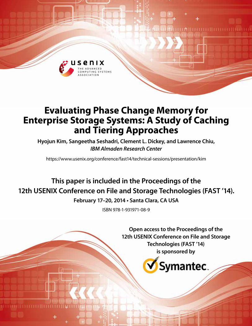
Figure 8: The best IOPS/$ for Retail store workload withvaried PCM parameters
skewed than the retail and bank workloads; approxi-mately 20% of the storage capacity receives about 52%of the read traffic and 23% of the write traffic. But readto write ratio is about 10 : 1, which is the most read dom-inant among the three workloads.
According to Figures 7(b) and (c), the best combina-tion from static data placement consists of PCM (82%)+ flash (10%) + HDD (8%), and calculated IOPS/$ valueis 4,045, which is about 2.2× better than the best com-bination without PCM: 84% flash + 16% HDD yielding1,853; the best combination from dynamic tiering simu-lation consists of PCM (96%) + flash (4%), and the ob-tained IOPS/$ value is 2,726. This value is about 66%higher than the best combination without PCM: 100%flash yielding 1,641 IOPS/$.
4.6 Sensitivity analysis for tieringThe simulation parameters are based on our best effortestimation of market price and the current state of PCMtechnologies, or based on discussions with experts. How-ever, PCM technology and its markets are still evolv-ing, and there are uncertainties about its characteristicsand pricing. To understand the sensitivity of our simu-lation results to PCM parameters, we tried six variationsof PCM parameters in three aspects: read performance,write performance, and price. For each aspect, we triedhalf-size and double-size values. For instance, we tested4.35 µs and 13.4 µs instead of the original 6.7 µs forPCM 4 KiB read latency.
Figure 8 shows the highest IOPS/$ value for varyingPCM parameters. We observe that our IOPS/$ measure ismost sensitive to PCM price. If PCM is only twice as ex-pensive as flash while maintaining its read and write per-formance, the PCM (38%) + flash (62%) configurationcan yield about 126% higher IOPS/$ (3,878); if PCM is8× more expensive than flash, PCM (5%) + flash (95%)configuration yields 1,921, which is 12% higher than theIOPS/$ value from the best configuration without PCM.
Interestingly, the configuration with twice slower
PCM write latency yields an IOPS/$ of 2,806, whichis slightly higher than the baseline value (2,757). Thatmay happen because the dynamic tiering algorithm isnot perfect. With the static optimal placement method,2× longer PCM write latency results in 3,216, which islower than the original value of 3,220.
4.7 Summary of tiering simulation
Based on the results above, we observe that PCM can in-crease IOPS/$ value by 12% (bank) to 66% (telecommu-nication company) even assuming that PCM is 4× moreexpensive than flash. These results suggest that PCM hashigh potential as a new component for enterprise storagesystems in a multi-tiered environment.
5 Workload simulation for server caching
Server-side caching is gaining popularity in enterprisestorage systems today [5, 10, 11, 12, 16, 20, 24]. Byplacing frequently accessed data close to the applicationon a locally attached (flash) cache, network latencies areeliminated and speedup is achieved. The remote storagenode benefits from decreased contention and the overallsystem throughput increases.
At first glance PCM SSD seems to be promising forserver-side caching, considering the 16× faster read timecompared to eMLC flash SSD. But given that PCM ismore expensive and slower for write than flash, will PCMbe a cost effective alternative? To address this ques-tion we use a second set of real-world traces to simu-late caching performance. The prior set of traces usedfor tiered storage simulation could not be used to evalu-ate cache performance since the traces were summarizedspatially and temporally at a coarse granularity. Threenew IO-by-IO traces are used: 1) a 24 hour trace from amanufacturing company, 2) a 36 hours trace from a me-dia company, and 3) a 24 hour trace from a medical ser-vice company. We chose three cache friendly workloads– highly skewed and read intensive – since our goal wasto compare PCM and flash for server-side caching sce-narios.
5.1 Cache simulation
We built a cache simulator using an LRU cache replace-ment scheme, 4 KiB page size, and write-through policy,which are the typical choices for enterprise server-sidecaching solutions. The simulator supports both singletier and hybrid (i.e. multi-tier) cache devices to test aconfiguration using PCM as a first level cache and flashas a second level cache. Our measurements (Table 2) areused for PCM and flash SSDs, and for networked storage

42 12th USENIX Conference on File and Storage Technologies USENIX Association
Table 3: Networked storage related parameters from [12]
Network base latency 8.2 µs / packetNetwork data latency 1 ns / bit
File server fast read 92 µs / 4 KiBFile server slow read 7,952 µs / 4 KiB
File server write 92 µs / 4 KiBFile server fast read rate 90%
Table 4: Cache simulation parameters
PCM eMLC Net. Storage
4 KiB R. Lat. 6.7 µs 108.0 µs 919.0 µs4 KiB W. Lat. 128.3 µs 37.1 µs 133.0 µsNorm. Cost 4 1 –
we use 919 µs and 133 µs for 4 KiB read and write, re-spectively. These numbers are based on the timing modelparameters (Table 3) from previous work [12]; networkoverhead for 4 KiB is calculated as 41.0 µs (8.2 µs baselatency + (4,096 × 8) bits × 1 ns), write time is 133 µs(write time 92 µs + network overhead 41 µs), and readtime is 919 µs (90% × fast read time 92 µs + 10% ×slow read time 7,952 µs + network overhead 41 µs).
The simulator captures the total number of read andwrite I/Os to the caching device and the networked stor-age separately, and then calculates average read latencyas our evaluation metric; with write-through policy, writelatency cannot be improved.
We vary the cache size from 64 GiB to a size that islarge enough to hold the entire dataset. We then calcu-late the average read latency for all-flash and all-PCMconfigurations.
Next, we compare the cache performance for all-PCM,all-flash, and PCM and flash hybrid combinations havingthe same cost.
5.2 Result 1: Manufacturing company
The first trace is from the storage server of a manufactur-ing company, running an On-Line Transaction Process-ing (OLTP) database on a ZFS file system.
Figure 9(a) shows the cumulative distribution as wellas the total amount of read and write I/O traffic for thisworkload. The total accessed capacity (during 24 hours)is 246.5 GiB, the total amount of read traffic is 3.8 TiB,and the total amount of write traffic is 1.1 TiB. The work-load exhibits strong skew: 20% of the storage capacityreceives 80% of the read traffic and 84% of the writetraffic.
Figure 9(b) shows the average read latency (Y-axis)for flash and PCM with different cache sizes. From the
0
20
40
60
80
100
0 20 40 60 80 100
Cum
ula
tive a
mount (%
)
Portion (%) of total accessd capacity (246.5 GiB)
Write
Read
Amount of Read Amount of Write
3.8 TiB
1.1 TiB
(a) CDF and I/O amount
0 20 40 60 80
100 120 140 160 180 200
64 GiB 128 GiB 256 GiB
Ave
rag
e R
ea
d L
at.
(µ
s)
Cache Size
187.7
151.0141.4
104.5(-44%)
59.5(-61%) 47.7
(-66%)
FlashPCM
(b) Average read latency
0
50
100
150
200
250
300
350
Flash64G
PCM16G
P8G+F32G
P4G+F48G
Flash128G
PCM32G
P16G+F64G
P8G+F96G
Flash256G
PCM64G
P32G+F128G
P16G+F192GA
vera
ge R
ead L
at. (
µs)
+29.3%
+1.5%
-38.3%
(c) Average read latency for even cost configurations
Figure 9: Cache simulation result for manufacturingcompany trace
results, we see that PCM can provide an improvement of44–66% over flash. Note that this figure assumes equalamount of PCM and flash and hence the PCM cachingsolution results in 4 times higher cost than an all-flashsetup (Table 4).
Next, Figures 9(c) shows average read latency forcost-aware configurations. The results are divided intothree groups. Within each group, we vary the ratio ofPCM and flash while keeping the cost constant. Forthe first two groups, all-flash configurations (64 GiB,128 GiB flash) show superior results to any configura-tion with PCM. For the third group (256 GiB flash), the32 GiBPCM + 128 GiB f lash combination shows about38% shorter average read latency than an all-flash con-figuration.
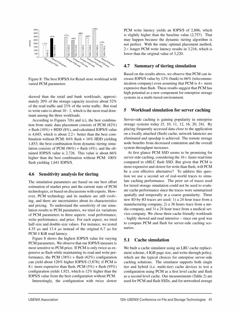
5.3 Result 2: Media company
The second trace is from the storage server of a mediacompany, also running an OLTP database.
The cumulative distribution and the total amount ofread and write I/O traffic are shown in Figure 10(a).The total accessed storage capacity is 4.0 TiB, the totalamount of read traffic is 5.7 TiB, and the total amount ofwrite traffic is 82.1 GiB. This workload is highly skewedand read intensive. Compared to other workloads, thisworkload has a larger working set size and a longer tail,
USENIX Association 12th USENIX Conference on File and Storage Technologies 43
0
20
40
60
80
100
0 20 40 60 80 100
Cum
ula
tive a
mount (%
)
Portion (%) of total accessd capacity (4.0 TiB)
Read
Write
Amount of Read Amount of Write
5.7 TiB
82.1 GiB
(a) CDF and I/O amount
0
50
100
150
200
250
300
64 GiB 128 GiB 256 GiB 512 GiB 1 TiB
Ave
rag
e R
ea
d L
at.
(µ
s)
Cache Size
208.4 205.1 200.2 194.4 193.9
129.9(-38%)
125.8(-39%)
119.9(-40%)
112.7(-42%)
112.1(-42%)
FlashPCM
(b) Average read latency
0
50
100
150
200
250
Flash64G
PCM16G
P8G+F32G
P4G+F48G
Flash128G
PCM32G
P16G+F64G
P8G+F96G
Flash256G
PCM64G
P32G+F128G
P16G+F192G
Avera
ge R
ead L
at. (
µs)
-35.8% -35.5% -35.5%
(c) Average read latency for even cost configurations
Figure 10: Cache simulation result for media companytrace
which results in a higher proportion of cold misses.Figure 10(b) shows average read latency (Y-axis) for
different cache configurations ranging from 64 GiB to1 TiB. Because of the large number of cold misses, theimprovements are less then those observed for the firstworkload: 38–42% shorter read latency than flash.
Figures 10(c) shows the simulation results for cost-aware configurations. Again, the results are divided intothree groups. Within each group, we vary the ratio ofPCM and flash while keeping the cost constant. Unlikethe previous workload (manufacturing company), PCMreduces read latency in all three groups by about 35%compared to flash.
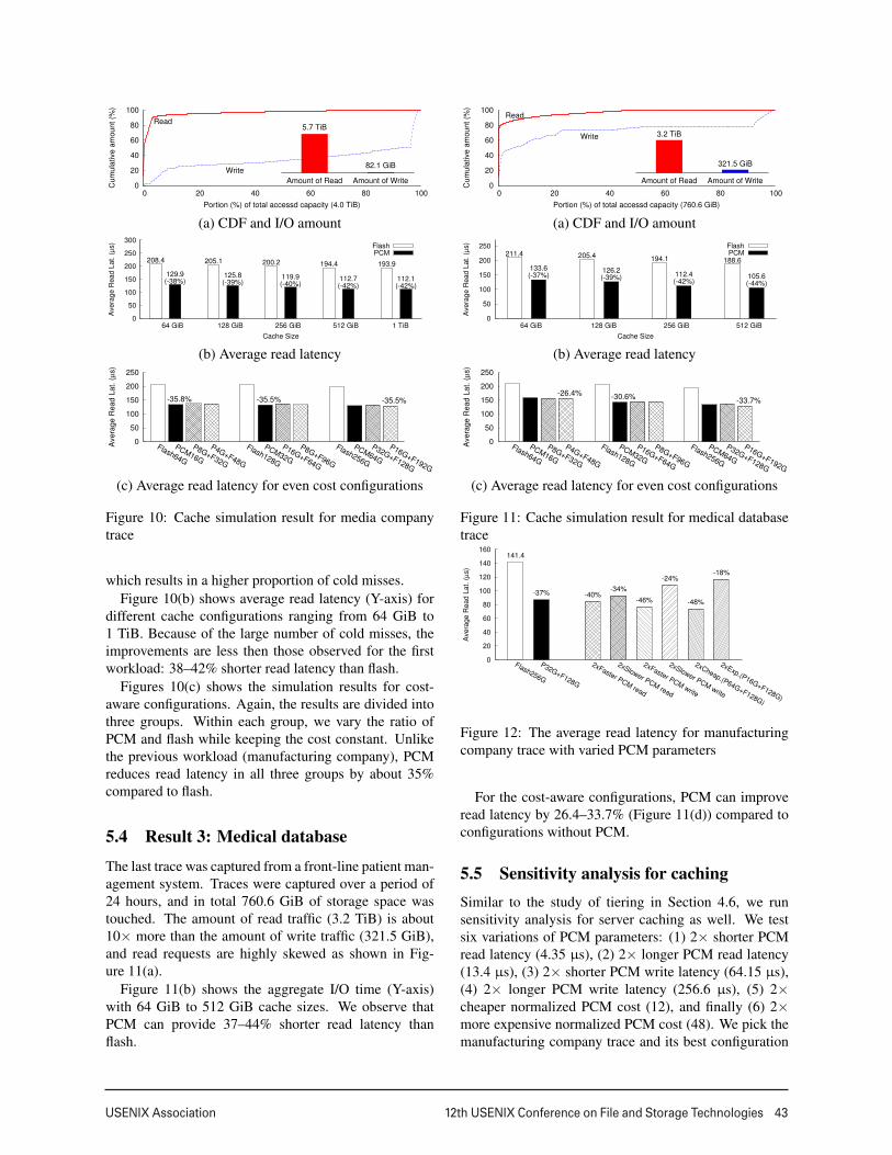
5.4 Result 3: Medical database
The last trace was captured from a front-line patient man-agement system. Traces were captured over a period of24 hours, and in total 760.6 GiB of storage space wastouched. The amount of read traffic (3.2 TiB) is about10× more than the amount of write traffic (321.5 GiB),and read requests are highly skewed as shown in Fig-ure 11(a).
Figure 11(b) shows the aggregate I/O time (Y-axis)with 64 GiB to 512 GiB cache sizes. We observe thatPCM can provide 37–44% shorter read latency thanflash.
0
20
40
60
80
100
0 20 40 60 80 100
Cum
ula
tive a
mount (%
)
Portion (%) of total accessd capacity (760.6 GiB)
Read
Write
Amount of Read Amount of Write
3.2 TiB
321.5 GiB
(a) CDF and I/O amount
0
50
100
150
200
250
64 GiB 128 GiB 256 GiB 512 GiB
Ave
rag
e R
ea
d L
at.
(µ
s)
Cache Size
211.4 205.4 194.1 188.6133.6(-37%)
126.2(-39%) 112.4
(-42%)105.6(-44%)
FlashPCM
(b) Average read latency
0
50
100
150
200
250
Flash64G
PCM16G
P8G+F32G
P4G+F48G
Flash128G
PCM32G
P16G+F64G
P8G+F96G
Flash256G
PCM64G
P32G+F128G
P16G+F192GA
vera
ge R
ead L
at. (
µs)
-26.4% -30.6%-33.7%
(c) Average read latency for even cost configurations
Figure 11: Cache simulation result for medical databasetrace
0
20
40
60
80
100
120
140
160
Flash256G
P32G+F128G
2xFaster PCM read
2xSlower PCM read
2xFaster PCM write
2xSlower PCM write
2xCheap.(P64G+F128G)
2xExp.(P16G+F128G)
Ave
rag
e R
ea
d L
at.
(µ
s)
141.4
-37% -40%-34%
-46%
-24%
-48%
-18%
Figure 12: The average read latency for manufacturingcompany trace with varied PCM parameters
For the cost-aware configurations, PCM can improveread latency by 26.4–33.7% (Figure 11(d)) compared toconfigurations without PCM.
5.5 Sensitivity analysis for cachingSimilar to the study of tiering in Section 4.6, we runsensitivity analysis for server caching as well. We testsix variations of PCM parameters: (1) 2× shorter PCMread latency (4.35 µs), (2) 2× longer PCM read latency(13.4 µs), (3) 2× shorter PCM write latency (64.15 µs),(4) 2× longer PCM write latency (256.6 µs), (5) 2×cheaper normalized PCM cost (12), and finally (6) 2×more expensive normalized PCM cost (48). We pick themanufacturing company trace and its best configuration

44 12th USENIX Conference on File and Storage Technologies USENIX Association
(PCM 32 GiB + flash 128 GiB).Figure 12 shows the simulated average read latencies
for varied configurations. The same trend is shown asobserved from the result for tiering (Figure 8); price cre-ates the biggest impacts; even when performing half aswell as our measured device, PCM still achieves 18–34%shorter average read latencies than all flash configura-tion.
5.6 Summary of caching simulation
Our cache simulation study with real-world storage ac-cess traces has demonstrated that PCM can improve ag-gregate I/O time by up to 66% (manufacturing companytrace) compared to a configuration that uses the samesize of flash. With cost-aware configurations, we showthat PCM can improve average read latency up to 38%(again, manufacturing company trace) compared to theflash only configuration.
From our results, we observe that the result from thefirst workload (manufacturing) is different from the re-sults of the second (media) and third (medical). Whileconfigurations with PCM offer significant performanceimprovement over any combination without PCM in thesecond and third workloads, we observe that that is trueonly for larger cache sizes in the first workload (i.e. Fig-ures 9(c). This can be attributed to the varying degreesof skewing in the workloads. The first workload exhibitsless skew (for read I/Os) than the second and third work-loads and hence has a larger working-set size. As a result,by increasing the cache size to capture the entire workingset for the first workload (data point PCM 32 GiB + flash128 GiB), we are eventually able to achieve a configura-tion that captures the active working-set.
These results point to the fact that PCM-based cachingoptions are a viable, cost-effective option to flash-basedserver-side caches, given a fitting workload profile. Con-sequently, analysis of workload characteristics is re-quired to identify critical parameters such as proportionof writes, skew and working set size.
6 Limitations and discussion
Our study into the applicability of PCM devices in real-istic enterprise storage settings has provided several in-sights. But we acknowledge that our analysis does haveseveral limitations: First, since our evaluation is basedon a simulation, it may not accurately represent systemconditions. Second, from our asynchronous I/O test (seesection 3.2), we observe that the prototype PCM devicedoes not exploit I/O parallelism much, unlike the eMLCflash SSD. This means that it may not be fair to say thatthe PCM SSD is 16× faster than the eMLC SSD for read,
because the eMLC SSD can handle multiple read I/O re-quests concurrently. It is a fair concern if we ignore thecapacity of the SSDs. The eMLC flash SSD has 1.8 TiBcapacity while the PCM SSD has only 64 GiB capacity.We assume that as the capacity of PCM SSD increases,its parallel I/O handling capability will increase as well.Finally, in order to understand long-term architecturalimplications, longer evaluation runs may be required forperformance characterization.
In this study, we approach PCM as storage rather thanmemory, and our evaluation is focused on average per-formance improvements. However, we believe that thePCM technology may be capable of much more. Asshown in our I/O latency measurement study, PCM canprovide well-bounded I/O response times. These per-formance characteristics will prove to be very useful toprovide Quality of Service (QoS) and multi-tenancy fea-tures. We leave exploration of these directions to futurework.
7 Conclusion
Emerging workloads seem to have an ever-increasing ap-petite for storage performance. Today, enterprise storagesystems are actively adopting flash technology. However,we must continue to explore the possibilities of next gen-eration non-volatile memory technologies to address in-creasing application demands as well as to enable newapplications. As PCM technology matures and produc-tion at scale begins, it is important to understand its ca-pabilities, limitations and applicability.
In this study, we explore the opportunities for PCMtechnology within enterprise storage systems. We com-pare the latest PCM SSD prototype to an eMLC flashSSD to understand the performance characteristics of thePCM SSD as another storage tier, given the right work-load mixture. We conduct a modeling study to analyzethe feasibility of PCM devices in a tiered storage envi-ronment.
8 Acknowledgments
We first thank our shepherd Steven Hand and anonymousreviewers. We appreciate Micron for providing theirPCM prototype hardware for our evaluation study andanswering our questions. We also thank Hillery Hunter,Michael Tsao, and Luis Lastras for helping our experi-ments, and Paul Muench, Ohad Rodeh, Aayush Gupta,Maohua Lu, Richard Freitas, Yang Liu for their valuablecomments and help.

USENIX Association 12th USENIX Conference on File and Storage Technologies 45
References[1] AKEL, A., CAULFIELD, A. M., MOLLOV, T. I., GUPTA, R. K.,
AND SWANSON, S. Onyx: a protoype phase change memorystorage array. In Proceedings of the 3rd USENIX conference onHot topics in storage and file systems (Berkeley, CA, USA, 2011),HotStorage’11, USENIX Association, pp. 2–2.
[2] AKERMAN, J. Toward a universal memory. Science 308, 5721(2005), 508–510.
[3] ATHANASSOULIS, M., BHATTACHARJEE, B., CANIM, M.,AND ROSS, K. A. Path Processing using Solid State Storage.In Proceedings of the 3rd International Workshop on Acceler-ating Data Management Systems Using Modern Processor andStorage Architectures (ADMS 2012) (2012).
[4] BEDESCHI, F., RESTA, C., ET AL. An 8mb demonstrator forhigh-density 1.8v phase-change memories. In VLSI Circuits,2004. Digest of Technical Papers. 2004 Symposium on (2004),pp. 442–445.
[5] BYAN, S., LENTINI, J., MADAN, A., PABON, L., CONDICT,M., KIMMEL, J., KLEIMAN, S., SMALL, C., AND STORER,M. Mercury: Host-side flash caching for the data center. InMass Storage Systems and Technologies (MSST), 2012 IEEE 28thSymposium on (2012), pp. 1–12.
[6] DELL. 300 gb 15,000 rpm serial attached scsi hotplug hard drivefor select dell poweredge servers / powervault storage.
[7] DELL. Dell Enterprise Hard Drive and Solid-State Drive Spec-ifications. http://i.dell.com/sites/doccontent/
shared-content/data-sheets/en/Documents/
enterprise-hdd-sdd-specification.pdf.
[8] DELL. LSI Logic Nytro WrapDrive BLP4-1600 - Solid StateDrive -1.6 TB - Internal. http://accessories.us.dell.
com/sna/productdetail.aspx?sku=A6423584.
[9] EMC. FAST: Fully Automated Storage Tiering. http://www.
emc.com/storage/symmetrix-vmax/fast.htm.
[10] EMC. XtreamSW Cache: Intelligent caching software that lever-ages server-based flash technology and write-through caching foraccelerated application performance with data protection. http://www.emc.com/storage/xtrem/xtremsw-cache.htm.
[11] FUSION-IO. ioTurbine: Turbo Boost Virtualization. http://
www.fusionio.com/products/ioturbine.
[12] HOLLAND, D. A., ANGELINO, E., WALD, G., AND SELTZER,M. I. Flash caching on the storage client. In Proceedings of the11th USENIX conference on USENIX annual technical confer-ence (2013), USENIXATC’13, USENIX Association.
[13] HOYA, K., TAKASHIMA, D., ET AL. A 64mb chain feram withquad-bl architecture and 200mb/s burst mode. In Solid-State Cir-cuits Conference, 2006. ISSCC 2006. Digest of Technical Papers.IEEE International (2006), pp. 459–466.
[14] IBM. IBM FlashSystem 820 and IBM FlashSystem 720. http://www.ibm.com/systems/storage/flash/720-820.
[15] IBM. IBM System Storage DS8000 Easy Tier. http://www.
redbooks.ibm.com/abstracts/redp4667.html.
[16] IBM. IBM System Storage DS8000 Easy Tier Server.http://www.redbooks.ibm.com/Redbooks.nsf/
RedbookAbstracts/redp5013.html.
[17] IBM. IBM XIV Storage System. http://www.ibm.com/
systems/storage/disk/xiv.
[18] KIM, D., LEE, S., CHUNG, J., KIM, D. H., WOO, D. H., YOO,S., AND LEE, S. Hybrid dram/pram-based main memory forsingle-chip cpu/gpu. In Design Automation Conference (DAC),2012 49th ACM/EDAC/IEEE (2012), pp. 888–896.
[19] KIM, J. K., LEE, H. G., CHOI, S., AND BAHNG, K. I. A pramand nand flash hybrid architecture for high-performance embed-ded storage subsystems. In Proceedings of the 8th ACM interna-tional conference on Embedded software (New York, NY, USA,2008), EMSOFT ’08, ACM, pp. 31–40.
[20] KOLLER, R., MARMOL, L., SUNDARARAMAN, S., TALA-GALA, N., AND ZHAO, M. Write policies for host-side flashcaches. In Proceedings of the 11th USENIX conference on Fileand Storage Technologies (2013), FAST’13, USENIX Associa-tion.
[21] LEE, B. C., IPEK, E., MUTLU, O., AND BURGER, D. Archi-tecting phase change memory as a scalable dram alternative. InProceedings of the 36th annual international symposium on Com-puter architecture (New York, NY, USA, 2009), ISCA ’09, ACM,pp. 2–13.
[22] LEE, K.-J., ET AL. A 90nm 1.8v 512mb diode-switch pram with266mb/s read throughput. In Solid-State Circuits Conference,2007. ISSCC 2007. Digest of Technical Papers. IEEE Interna-tional (2007), pp. 472–616.
[23] MOGUL, J. C., ARGOLLO, E., SHAH, M., AND FARABOSCHI,P. Operating system support for nvm+dram hybrid main memory.In Proceedings of the 12th conference on Hot topics in operatingsystems (Berkeley, CA, USA, 2009), HotOS’09, USENIX Asso-ciation, pp. 14–14.
[24] NETAPP. Flash Accel software improves application per-formance by extending NetApp Virtual Storage Tier to en-terprise servers. http://www.netapp.com/us/products/
storage-systems/flash-accel.
[25] PURESTORAGE. FlashArray, Meet the new 3rd-generation FlashArray. http://www.purestorage.com/
flash-array/.
[26] QURESHI, M. K., FRANCESCHINI, M. M., JAGMOHAN, A.,AND LASTRAS, L. A. Preset: improving performance of phasechange memories by exploiting asymmetry in write times. In Pro-ceedings of the 39th Annual International Symposium on Com-puter Architecture (Washington, DC, USA, 2012), ISCA ’12,IEEE Computer Society, pp. 380–391.
[27] QURESHI, M. K., SRINIVASAN, V., AND RIVERS, J. A. Scal-able high performance main memory system using phase-changememory technology. In Proceedings of the 36th annual inter-national symposium on Computer architecture (New York, NY,USA, 2009), ISCA ’09, ACM, pp. 24–33.
[28] RAOUX, S., BURR, G., BREITWISCH, M., RETTNER, C.,CHEN, Y., SHELBY, R., SALINGA, M., KREBS, D., CHEN, S.-H., LUNG, H. L., AND LAM, C. Phase-change random accessmemory: A scalable technology. IBM Journal of Research andDevelopment 52, 4.5 (2008), 465–479.
[29] SIE, C. Memory Cell Using Bistable Resistivity in AmorphousAs-Te-Ge- Film. Iowa State University, 1969.