evaluation board user’s guide for tdnext tdaip01 … · evaluation board user’s guide for...
TRANSCRIPT

TDAIP01 EVB
EVB for TDAIP01 Rev 1.1 User’s Guide
April 2017 - Rev 1.1 cameramodules.td-next .com Page 1
EVALUATION BOARD USER’S GUIDE FOR TDNEXT TDAIP01 MO DULE

TDAIP01 EVB
EVB for TDAIP01 Rev 1.1 User’s Guide
April 2017 - Rev 1.1 cameramodules.td-next .com Page 2
Disclaimer : The information in this document is provided in connection with Telecom Design products. No license, express or implied, by estoppel or otherwise, to any intellectual property right is granted by this document or in connection with the sale of Telecom Design products. TELECOM DESIGN ASSUMES NO LIABILITY WHATSOEVER AND DISCLAIMS ANY EXPRESS, IMPLIED OR STATUTORY WARRANTY RELATING TO ITS PRODUCTS INCLUDING, BUT NOT LIMITED TO, THE IMPLIED WARRANTY OF MERCHANTABILITY, FITNESS FOR A PARTICULAR PURPOSE, OR NON-INFRINGEMENT. IN NO EVENT SHALL TELECOM DESIGN BE LIABLE FOR ANY DIRECT, INDIRECT, CONSEQUENTIAL, PUNITIVE, SPECIAL OR INCIDENTAL DAMAGES (INCLUDING, WITHOUT LIMITATION, DAMAGES FOR LOSS OF PROFITS, BUSINESS INTERRUPTION, OR LOSS OF INFORMATION) ARISING OUT OF THE USE OR INABILITY TO USE THIS DOCUMENT, EVEN IF TELECOM DESIGN HAS BEEN ADVISED OF THE POSSIBILITY OF SUCH DAMAGES. Telecom Design makes no representations or warranties with respect to the accuracy or completeness of the contents of this document and reserves the right to make changes to specifications and product descriptions at any time without notice. Telecom Design does not make any commitment to update the information contained herein. Unless specifically provided otherwise, Telecom Design products are not suitable for, and shall not be used in, automotive applications. Telecom Design products are not intended, authorized, or warranted for use as components in applications intended to support or sustain life. © 2016-2017 Telecom Design S.A. All rights reserved. Telecom Design®, logo and combinations thereof, are registered trademarks of Telecom Design S.A. TDnext is a trademark of TDnext. Other terms and product names may be trademarks of other.

TDAIP01 EVB
EVB for TDAIP01 Rev 1.1 User’s Guide
April 2017 - Rev 1.1 cameramodules.td-next .com Page 3
Description
TDnext TDAIP01 is a compact module that mounts on a user PCB. The TDAIP01module features video, image and audio processing capabilities using a powerful hardware while maintaining a low cost and low power consumption (the TDAIP01 does not need an external DRAM). By simple configuration, the TDAIP01 module is ready to support simultaneous audio/video inputs, and to drive many external peripherals such as a 3G/4G modem, Wi-Fi module, SDCard, behave as an USB camera/mass storage/printer class device and also support SPI, UART and GPIOs interfaces for control functions. The integrated high performance processor supports H.264 and MJPEG compression. No firmware development is required: user only has to configure TDAIP01’s both working mode and peripheral settings. Hence, by using “easy” scripts files, the required functionalities can be activated, and actions to be performed are configured; the TDAIP01 can then work in stand-alone mode, no additional processor is required. The configuration setup may be performed early during product manufacturing. Video streaming over external Wi-Fi module or 3G/4G modem, microSD Card recording, connecting a PIR sensor, an external I/R LED for night vision, are some of the applications that may be achieved easily, only by a simple TDAIP01 module configuration. The TDAIP01 low power consumption makes it possible to design battery powered products thanks to the smart highly integrated processor. During video streaming, the H.264 compression uses only the integrated DRAM memory and does not require external additional DRAM chips, thus providing more integration, as well as lowering the cost and power consumption at the same time. The TDAIP01 module can be driven by a host processor if needed. Through several available interfaces like USB device, UART or SPI, a host may configure and receive a video streaming in real-time.

TDAIP01 EVB
EVB for TDAIP01 Rev 1.1 User’s Guide
April 2017 - Rev 1.1 cameramodules.td-next .com Page 4
CONTENT
1 Overview .......................................... .................................................................................. 5
1.1 Scope ............................................. ................................................................................................................... 5
1.2 Features .......................................... ................................................................................................................. 5
1.3 Relevant Documents ................................ ....................................................................................................... 7
2 Setting up the TDAIP01-EVB ........................ .................................................................... 8
2.1 Electrostatic Warning ............................. ........................................................................................................ 8
2.2 Packing List ...................................... ............................................................................................................... 8
2.3 Requirements ...................................... ............................................................................................................ 8
2.4 Getting Started ................................... ............................................................................................................. 8
3 TDAIP01-EVB Overview .............................. .................................................................... 13
3.1 Layout ............................................ ................................................................................................................. 13
3.2 Block Diagram ..................................... .......................................................................................................... 14
4 TDAIP01-EVB BOOT Mode Selection.................... ......................................................... 15
5 TDAIP01-EVB Power Management....................... .......................................................... 17
6 TDAIP01-EVB Interfaces ............................ ..................................................................... 21
6.1 Camera Interfaces ................................. ........................................................................................................ 21
6.2 Wi-Fi Interfaces................................... ........................................................................................................... 24
6.3 USB Interfaces .................................... ........................................................................................................... 25
6.4 SDCard Interface .................................. ......................................................................................................... 26
6.5 TDnext RF Module Interface ........................ ................................................................................................. 26
6.6 UART Interfaces ................................... ......................................................................................................... 26
6.7 User GPIO Interface ............................... ....................................................................................................... 27
6.8 PIR Sensor Interface .............................. ....................................................................................................... 28
6.9 Expansion Connector Interface ..................... .............................................................................................. 29
7 TDAIP01-EVB Internal Function Blocks .............. .......................................................... 30
7.1 Accelerometer ..................................... .......................................................................................................... 30
7.2 Stereo Audio Codec ................................ ...................................................................................................... 30
7.3 RTC ................................................................................................................................................................. 30
8 TDAIP01-EVB Schematics ............................ .................................................................. 31
9 TDAIP01-EVB Mechanical Drawing .................... ............................................................ 38

TDAIP01 EVB
EVB for TDAIP01 Rev 1.1 User’s Guide
April 2017 - Rev 1.1 cameramodules.td-next .com Page 5
1 Overview
This document provides a User’s Guide for the TDnext TDAIP01 Modules evaluation board (TDAIP01-EVB ). As an overview, this chapter gives the scope of this document and lists the board’s features. The document’s organization is then detailed.
1.1 Scope The TDAIP01-EVB provides a development and demonstration platform for the TDnext TDAIP01 module and software tools. This guide focuses on the TDAIP01-EVB evaluation board as a development platform for the TDnext TDAIP01 Modules.
1.2 Features The board’s main features are:
� TDAIP01 module in LGA108 package which provides:
� H.264 compression
� Baseline Profile: Level 3.0 for QVGA @30 fps
� Baseline Profile: Level 3.0 for VGA @30 fps
� Main Profile, Level 4.0 for 720p @30 fps
� MJPEG video compression
� PCM, ADPCM and AAC audio compression
� Wi-Fi driver for various chips
� 3G/4G modem drivers for various modules
� 256Kbytes + 2Mbytes Internal SRAM
� 2Mbytes Internal serial Flash
� 1x CIS (CMOS Image Sensor) DVP Parallel 10-bit interface
� CIS (CMOS Image Sensor) MiPi 2-lane interface
� 1x DVP 30-pin mezzanine connector
� 1x I2C master interface
� 1x I2S Stereo audio codec interface
� 1x SDCard interface
� 1x SDIO interface
� 1x USB 2.0 Host interface
� 1x USB 2.0 Device interface
� 2x UART interfaces
� 1x SPI interface
� 7x USR GPIOs
� 7x CIS (CMOS Image Sensor) GPIOs
� Adjustable power supply for external camera
� AVDD : From 1.2V to 3.3V
� DVDD : From 1.25V to 3.3V
� DOVDD : From 1.2V to 3.3V
� 3V-5V power management

TDAIP01 EVB
EVB for TDAIP01 Rev 1.1 User’s Guide
April 2017 - Rev 1.1 cameramodules.td-next .com Page 6
� 3x Adjustable power supply interfaces
� 1x Micro USB connector for power supply
� 1x screw header for external power supply
� 1x MiPi FPC-30-pin connector
� 1x DVP FPC-24 pin connector
� 1x DVP external 2.54 mm pitch connector
� 1x USB-A Host connector
� 1x Micro USB Device connector
� 2x Wi-Fi modules with SMA connectors (Marvel 88W8782 and ESP8266EX)
� 1x SDCard connector
� 1x PIR motion detection module connector
� 1x 2.5 mm phone jack for stereo headphones
� 8x IR LEDs
� 1x TDnext RF module interface
� 1x 40-pin 2.54 mm pitch expansion connector
� 1x BOOT RAM and 1 BOOT ROM interface
� 1x WM8960 I2S stereo audio codec chip
� 2x MEMs microphones
� 1x LIS3DH 3-axis accelerometer chip
� 1x M41T81S I2C RTC chip with CR2032 battery back-up holder
� 3x hardware reset buttons
� 1x user button
� 16x LEDs for individual function block power indication
� 2x user LEDs Figure 1 provides an overview of the TDAIP01-EVB board.

TDAIP01 EVB
EVB for TDAIP01 Rev 1.1 User’s Guide
April 2017 - Rev 1.1 cameramodules.td-next .com Page 7
Figure 1. TDAIP01-EVB overview
1.3 Relevant Documents This document provides a hardware overview for the TDAIP01 EVB board. Additional information on the TDnext TDAIP01 modules can be found in the following documents:
• TDAIP01 Datasheet • TDAIP01 Reference Manual
These documents are available on the TDnext Web site developer’s area (http://cammodules.td-next.com/)

TDAIP01 EVB
EVB for TDAIP01 Rev 1.1 User’s Guide
April 2017 - Rev 1.1 cameramodules.td-next .com Page 8
2 Setting up the TDAIP01-EVB
This section helps you set up the TDAIP01-EVB for the first time. Please consider first the electrostatic warning to avoid damaging the board, then discover the hardware and software required to operate the board. The procedure to power up the board is given, and a description of the default board behavior is detailed.
2.1 Electrostatic Warning The TDAIP01-EVB board is an ESD sensitive device, appropriate precautions should be taken during the TDAIP01-EVB utilization.
2.2 Packing List The TDAIP01-EVB is delivered in a box containing:
� A Wi-Fi antenna
� 2x TTL-232R-3V3 FTDI USB to TTL Serial Cable (3.3V)-1.8m
� A wall-wart 5V DC power supply with USB A output connector
� A CR2032 coin cell
� A Class 10 Micro SD Card
� An Ethernet PCB adapter
� An “ETH WIZ click board” featuring a WIZ5500 Ethernet chip and RJ45 socket
� 2x TDAIP01-SOFTxxxx modules
� A TD7740-FBAC CGA camera module (HFOV 90° w/ IR filter, FPC 25 mm)
� A TDM114-FBPC 720p camera module (HFOV 90° w/ IR filter, FPC 25 mm)
� A TD5640-FBGC 5Mp camera module (HFOV 55° w/ IR filter, mezzanine connector)
� The TDAIP01-EVB board itself
2.3 Requirements In order to set up the TDAIP01-EVB board, the following additional items are required:
� This document
� A PC running Windows XP, Windows Server 2003, Windows Vista operating system or above (this is only required to be able to flash the device using the provided utility program, for a simple connection to the module, any operating system for which FTDI devices are supported should work)
� A serial terminal emulation program running on the PC, such as:
• HyperTerminal (included in Windows 9x/2000/XP) • PuTTY (http://www.chiark.greenend.org.uk/~sgtatham/putty/download.html) • RealTerm (http://realterm.sourceforge.net/)
� The FTDI Virtual COM Port Driver (VCD) which is appropriate for your machine: (http://www.ftdichip.com/Drivers/VCP.htm)
2.4 Getting Started For a quick demonstration, the TDAIP01-EVB will be configured to record from a provided TDM114 camera module to an SD Card, while displaying debug information from the board over an USB virtual serial communication port into a
TDAIP01 EVB
EVB for TDAIP01 Rev 1.1 User’s Guide
April 2017 - Rev 1.1 cameramodules.td-next .com Page 9
serial terminal emulation software running on a PC. The board will be powered using a standard USB cable connected to the same PC. To set up the TDAIP01-EVB for this first use, several simple steps must be performed in turn:
1. Set up the camera module 2. Insert the SD Card 3. Select the power source 4. Set up the DEBUG UART 5. Power up the board by connecting the USB cable between the TDAIP01-EVB board and the PC
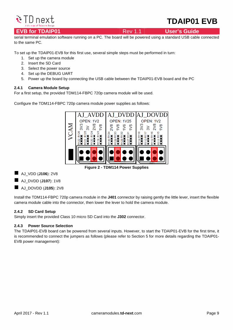
2.4.1 Camera Module Setup For a first setup, the provided TDM114-FBPC 720p camera module will be used. Configure the TDM114-FBPC 720p camera module power supplies as follows:
Figure 2 - TDM114 Power Supplies
� AJ_VDD (J106): 2V8
� AJ_DVDD (J107): 1V8
� AJ_DOVDD (J105): 2V8
Install the TDM114-FBPC 720p camera module in the J401 connector by raising gently the little lever, insert the flexible camera module cable into the connector, then lower the lever to hold the camera module.
2.4.2 SD Card Setup Simply insert the provided Class 10 micro SD Card into the J302 connector.
2.4.3 Power Source Selection The TDAIP01-EVB board can be powered from several inputs. However, to start the TDAIP01-EVB for the first time, it is recommended to connect the jumpers as follows (please refer to Section 5 for more details regarding the TDAIP01-EVB power management):

TDAIP01 EVB
EVB for TDAIP01 Rev 1.1 User’s Guide
April 2017 - Rev 1.1 cameramodules.td-next .com Page 10
Figure 3. Powering start-up configuration
1) Put a jumper in front of “USB DEVICE” on “POWER SUPPLY USED” jumper block J104 to select the power supply source from the micro USB device connector
2) Set the jumper in the “DOVDD” position on “VDEBUG” jumper block J103 to use DOVDD for supplying the DEBUG UART
3) Set the jumper in the “500mA” position on the “IMAX” jumper block J311 to set the TDAIP01-EVB board current consumption limit to a value compatible with the USB specification
4) Put a jumper on the “ACTIVE BLOCK ” / “ON/OFF LED” jumper block J500 to enable all the LEDs to visualize power supplies for all onboard active blocks
5) Put a jumper in the “CIS_DOVDD” position on the “DOVDD_TDAIP01” jumper block J1001 to connect the CMOS Image Sensor (CIS) DOVDD to feed the TDAIP01 DOVDD
6) Put 4 jumpers in front of “DOVDD”, “DVDD”, “AVDD” and “VIN_TDAIP01” on “ACTIVATED POWER SUPPLY ” jumper block J108 to activate the corresponding power supplies
2.4.4 DEBUG UART Setup First plug one TTL-232R-3V3 FTDI USB to TTL Serial Cable USB A plug into an available USB port on the PC, which may install the corresponding FTDI Virtual Communication Port (VCP) if required. Please follow the installation instructions for your Operating System available at http://www.ftdichip.com/Support/Documents/InstallGuides.htm. As the serial terminal emulation software will require the (virtual) port corresponding to the newly attached FTDI device, the best way to find it is to use Window’s “Device Manager ” from the Control Panel, by clicking on the “System ” icon and selecting the “Hardware ” tab and pressing the “Device Manager… ” button. Please locate and unfold the “Ports

TDAIP01 EVB
EVB for TDAIP01 Rev 1.1 User’s Guide
April 2017 - Rev 1.1 cameramodules.td-next .com Page 11
(COM & LPT) ” entry into the device tree list: you should see an “USB Serial Port (COM x)” entry corresponding to the newly attached TDAIP01-EVB device. If unsure, you can safely unplug/replug the USB cable to observe the changes into the “Device Manager ” window. Please write down this “COMx” information, so you can provide it later to the serial terminal emulation software. You can then close Windows’s “Device Manager ” window. For other Operating Systems, please find the corresponding port with the appropriate tools. Connect the other end of the FTDI cable to the TDAIP01-EVB board into the “FTDI” J9 connector as illustrated below:
Figure 4. FTDI cable connection
Now launch your selected serial terminal emulation software, and set up the following serial communication parameters:
� Port as obtained from Window’s “Device manager” or OS tool
� 115200 bps
� 8 data bits
� No parity
� 1 stop bit
� No hardware/software flow control
2.4.5 Board Power Up Connect the micro USB cable into an available USB host port on the PC and on in the TDAIP01-EVB board into the micro USB socket J310 as illustrated below:
Figure 5. Micro USB cable connection

TDAIP01 EVB
EVB for TDAIP01 Rev 1.1 User’s Guide
April 2017 - Rev 1.1 cameramodules.td-next .com Page 12
The onboard LEDs should light up to show the functional blocks that are activated, and messages should be displayed into the terminal emulator. The default firmware and script pre-configured into the TDAIP01 module will enable recording a video clip onto the Micro SD Card upon button press on the onboard CIS_GPIO5 button (SW503). The recording automatically stops after 15 s or upon another button press on the same button. You can then take the Micro SD Card out and insert it into a PC to play it back using a multimedia player able to decode AVI files using H.264 video / AAC audio compressions.

TDAIP01 EVB
EVB for TDAIP01 Rev 1.1 User’s Guide
April 2017 - Rev 1.1 cameramodules.td-next .com Page 13
3 TDAIP01-EVB Overview
The TDAIP01-EVB board provides access to the different TDnext TDAIP01 module interfaces using separate circuit blocks.. This section presents the different functionalities available in this EVB. For obtaining the most detailed information on a particular board feature, please refer to the detailed description in the following sections or to the schematics presented in section 9.
3.1 Layout
Figure 6. TDAIP01-EVB Top view

TDAIP01 EVB
EVB for TDAIP01 Rev 1.1 User’s Guide
April 2017 - Rev 1.1 cameramodules.td-next .com Page 14
3.2 Block Diagram
Figure 7. TDAIP01 block diagram

TDAIP01 EVB
EVB for TDAIP01 Rev 1.1 User’s Guide
April 2017 - Rev 1.1 cameramodules.td-next .com Page 15
4 TDAIP01-EVB BOOT Mode Selection
The TDAIP01 features an integrated ROM-based bootloader, ensuring a fail-safe mechanism to recover a module even when no firmware is available. During normal operation, this ROM-based bootloader launches a second-stage RAM-based bootloader read from the integrated Flash memory or received through various communication interfaces, that in turn will launch the main application or enter some specific provisioning or configuration modes. These two bootloaders are configurable using the TDAIP01 module BOOTx I/Os that are available on the TDAIP01-EVB as two adjacent jumper blocks J300 and J314, detailed in Figure 8 :
Figure 8. ROM/RAM bootloader
4.1.1 ROM Bootloader Despite its small size, the built-in ROM bootloader is able to boot the module into various modes, depending on BOOTx I/O configuration (Table 1):
o Start the second-stage RAM Bootloader o Perform a Low-level firmware upgrade from USB device
BOOT3 BOOT2 BOOT1 BOOT0 TDAIP01 Default : Start Bootloader RAM 0 1 0 0
Table 1. ROM Bootloader configuration All other BOOTx I/O configurations are unsupported.
4.1.2 RAM Bootloader The second-stage RAM bootloader provides additional flexibility by performing a more complete hardware configuration (clocks, PLL, memory access optimizations, etc.), then selecting the user operation mode to launch, depending on additional BOOTx I/O configuration (Table 2):
BOOT7 BOOT6 BOOT5 BOOT4 TDAIP01 Default : Application startup 0 0 0 0 Depending on CIS_GPIO5 value : - 0: Configuration mode over UART1 - 1: Application startup
0 0 0 1
Configuration mode over UART0 1 0 0 0 Configuration mode over UART1 1 0 0 1 Interactive mode over UART0 1 0 1 0 Interactive mode over UART1 1 0 1 1 Upgrade mode over UART0 1 1 0 0 Upgrade mode over UART1 1 1 0 1
Table 2. RAM Bootloader configuration

TDAIP01 EVB
EVB for TDAIP01 Rev 1.1 User’s Guide
April 2017 - Rev 1.1 cameramodules.td-next .com Page 16
All other BOOTx I/O configurations are unsupported.

TDAIP01 EVB
EVB for TDAIP01 Rev 1.1 User’s Guide
April 2017 - Rev 1.1 cameramodules.td-next .com Page 17
5 TDAIP01-EVB Power Management
In order to evaluate the TDAIP01 module capabilities in the best conditions, the TDAIP01-EVB board provides a large choice of power supply sources and a flexible power distribution scheme that allows enabling / disabling the numerous functional blocks that are available onboard.
Figure 9. TDAPI01-EVB power distribution
5.1.1 External Power Supply Selection and Current L imitation Four external power supply sources are possible:
- A +3.3 V / 2 A power supply voltage applied to the J102 green screw terminal block - A +2.2 V to +5 V / 500 mA power supply voltage applied to the J102 green screw terminal block - A +5 V / 500 mA power supply voltage applied to the J101 micro USB power-supply-only connector - A +5 V / 500 mA power supply voltage applied to the J310 micro USB device connector
Except when a +3.3 V / 2 A power supply voltage is used to directly power the board, the TDAIP01-EVB board onboard voltage regulators provide both a +5V and +3.3V internal power supply rail.

TDAIP01 EVB
EVB for TDAIP01 Rev 1.1 User’s Guide
April 2017 - Rev 1.1 cameramodules.td-next .com Page 18
In order to select the desired TDAIP01-EVB power supply source, a jumper must be installed on the on “POWER SUPPLY USED” jumper block J104 (see Figure 10 ):
- µUSB Power (5V) - USB Device - EXTERNAL_3V3
The “USB Device ” and “µUSB Power (5V) ” power sources are both current-limited to 500mA. If one of these options is used, the jumper on the “IMAX” jumper block J311 must also be set in the “500mA” position (see Figure 11 ). However, if the “EXTERNAL 3V3 ” source is taken from the J102 green screw terminal with an externally regulated applied regulated voltage of +3.3V, the current limit can be increased up to 2A by setting the “IMAX” jumper block J311 in the “2A (EXT 3V3)” position.
Figure 10. Power Supply indication
Figure 11. Imax indication
5.1.2 Power Supply Distribution Individual TDAIP01-EVB functional blocks can be disabled by removing jumpers selectively in order to reduce the total current consumption. As a convenience, these jumpers can also be used to measure the current consumption of each individual block by replacing them by an ammeter (see Figure 12 and Figure 13 ).
Figure 12. General power supply distribution
Figure 13. Wi-Fi Power supply distribution
- DOVDD_TDAIP01: this is the camera interface I/O power domain. This voltage can be set to direct +3.3V rail
power supply or to the CIS_DOVDD voltage power supply provided by the TDAIP01 module using the J1001 jumper block. Note : this jumper must be configured before applying the power supply to the board
- VIN TDAIP01: this is the TDAIP01 module input power supply when a jumper is set in this position on the J108 jumper block. Note : this jumper must be configured before applying the power supply to the board
- DOVDD, DVDD and AVDD are the voltage power supplies provided by the TDAIP01 module to the camera when jumpers are fitted on the J108 jumper block in the corresponding positions

TDAIP01 EVB
EVB for TDAIP01 Rev 1.1 User’s Guide
April 2017 - Rev 1.1 cameramodules.td-next .com Page 19
- RF: the +3.3 V voltage rail is fed to the TDnext RF module on connector J303 when a jumper is set on the J109 jumper block in the corresponding position
- SDCARD: the +3.3 V voltage rail is fed to the SDCard connector J302 when a jumper is set on the J109 jumper block in the corresponding position
- I2S: the +3.3 V voltage rail is fed to the WM8960 I2S stereo audio codec chip U300 when a jumper is set on the J109 jumper block in the corresponding position
- RTC: the +3.3 V voltage rail is fed to the M41T81S RTC chip U305 when a jumper is set on the J109 jumper block in the corresponding position
- ACC: the +3.3 V voltage rail is fed to the LIS3DH 3-axis accelerometer chip U200 when a jumper is set on the J109 jumper block in the corresponding position
- 88W8: the +3.3 V voltage rail is fed to the 88W8782 Wi-Fi module U304 when a jumper is set on the J307 jumper block in the corresponding position
- ESP: the +3.3 V voltage rail is fed to the ESP8266 Wi-Fi chip U302 when a jumper is set on the J307 jumper block in the corresponding position
5.1.3 External Camera Power Supply Voltage Adjustme nts The TDAIP01 module is able to deliver up to three different power supplies to an external camera:
- CISAVDD is used for the camera analog power supply - CISDVDD is used for the camera digital power supply - CISDOVDD is used for the camera I/O power supply
CISAVDD, CISDVDD and CISDOVDD can be customized to meet the camera requirements using bias resistors. The TDAIP01-EVB offers the following possibilities (see Figure 14 ):
- CISAVDD and CISDOVDD can provide 1.2V, 1.8V, 2.8V, 3V and 3.3V - CISDVDD can provide 1.25V, 1.5V, 1.6V, 1.8V and 2.8V
Figure 14. External camera power supply selection
The recommended power supply configuration for the TD7740 and TD5640 camera modules is:
Figure 15. TD7740 and TD5640 power supply

TDAIP01 EVB
EVB for TDAIP01 Rev 1.1 User’s Guide
April 2017 - Rev 1.1 cameramodules.td-next .com Page 20
The recommended power supply configuration for the TDM114 camera modules is:
Figure 16. TDM114 power supply
5.1.4 I2C Interface The TDAIP01 module I²C interface implements the I2C master mode only. It actually supports only a subset of the full I2C specification known as the Serial Camera Control Bus (SCCB). For additional information, please refer to the I2C Bus Specification or to the SCCB Functional Description. On the TDAIP01-EVB, this interface is used by the following devices:
- Camera sensor control (variable I2C address) - 3-axis Accelerometer sensor (address is 0x30h or 0x32h, depending on R322 / R323 configuration) - Stereo audio codec control (address is 0x34h) - RTC (address is 0xD0h)
The TDAIP01 I²C bus uses the DOVDDTDAIP01 power domain interface for the camera sensor control, as it must change according to the plugged camera. However, all the other devices require a 3.3V power domain. In order to adapt the voltage levels, an NXP PCA9517 I²C level shifter chip is used between the camera I2C bus and I2C bus used by the other devices. For additional information, please refer to the PCA9517 datasheet.
Figure 17. I²C level shift reference circuit

TDAIP01 EVB
EVB for TDAIP01 Rev 1.1 User’s Guide
April 2017 - Rev 1.1 cameramodules.td-next .com Page 21
6 TDAIP01-EVB Interfaces
This section describes the different TDAIP01-EVB board external interfaces.
6.1 Camera Interfaces As the main purpose for the TDAIP01-EVB board is to evaluate the TDAIP01 video module, the camera interfaces are of utmost importance. Not counting for the optional on-module TDAIP01 camera connector, the TDAIP01-EVB board provides a camera clock and 3 different camera module connectors:
- A 24-pin FPC connector J401 for an 8 or 10-bit parallel (DVP) CMOS camera module - A 30-pin FPC connector J400 for a MiPi CMOS camera module - A 2x16-pin 2.54 mm pitch receptacle J402 for an external 8 or 10-bit parallel (DVP) CMOS camera sensor or
module
6.1.1 24-pin FPC Connector The J401 connector is a 24-pin FPC ‘FH12-24S-0.5SH’ connector that provides a CMOS 8 or 10-bit parallel camera interface. The connector pinout is given in the following figure and table.
Figure 18. FH12-24S-0.5SH
Connector
Table 3. FH12-24S-0.5SH connector pin descriptions
Pin number
Signal Name
Pin Type Function
1 CIS_GPIO6 I/O SENSOR GPIO6
2 GND Ground TDAIP01-EVB ground
3 SDA I/O I2C data
4 CISAVDD Input Analog supply Voltage of camera
5 SCL Input I2C clock
6 CIS_GPIO0 I/O SENSOR GPIO0
7 VSYNC Output Sensor vertical sync
8 CIS_GPIO4 I/O SENSOR GPIO4
9 HSYNC Output Sensor horizontal sync
10 CISDVDD Input Digital Supply Voltage of camera
11 CISDOVDD Input Interface Supply Voltage of camera
12 Y9 Output Digital video input data 9
13 CAM Clock Input Input clock for camera. XLCK or TCXO present on EVB
14 Y8 Output Digital video input data 8
15 GND Ground TDAIP01-EVB ground
16 Y7 Output Digital video input data 7
17 PCLK Output Pixel clock Output
18 Y6 Output Digital video input data 6
19 Y2 Output Digital video input data 2
20 Y5 Output Digital video input data 5
21 Y3 Output Digital video input data 3
22 Y4 Output Digital video input data 4
23 Y1 Output Digital video input data 1
24 Y0 Output Digital video input data 0

TDAIP01 EVB
EVB for TDAIP01 Rev 1.1 User’s Guide
April 2017 - Rev 1.1 cameramodules.td-next .com Page 22
6.1.2 30-pin FPC Connector The J400 connector is a 30-pin ‘DF30RB-30DP-0.4V’ connector that provides a MiPi 2-lane CMOS camera interface. The connector pinout is given in the following figure and table.
Figure 19. DF30RB-30DP-0.4V Connector
Table 4. DF30RB-30DP-0.4V connector pin description s
Pin number
Signal Name
Pin Type Function Pin
number Signal Name
Pin Type Function
1 GND Ground TDAIP01-EVB ground 16 NC NC Not connected
2 AFVDD Input Regulated 2.8V power supply 17 MCN Output MIPI clock lane
differential negative
3 CISAVDD Input Analog supply Voltage of camera
18 CIS_GPIO0 I/O SENSOR GPIO0
4 CAM Clock Input Input clock for camera. XLCK or EVB-TCXO 19 MDP0 Output MIPI lane 0 differential
positive
5 GND Ground TDAIP01-EVB ground 20 CIS_GPIO1 I/O SENSOR GPIO1
6 SDA I/O I2C data 21 MDN0 Output MIPI lane 0 differential negative
7 CISDVDD Input Digital Supply Voltage of camera 22 NC NC Not connected
8 SCL Input I2C clock 23 NC NC Not connected
9 GND Ground TDAIP01-EVB ground 24 CIS_GPIO4 I/O SENSOR GPIO4
10 NC NC Not connected 25 NC NC Not connected
11 MDP1 Output MIPI lane 1 differential positive 26 NC NC Not connected
12 NC NC Not connected 27 GND Ground TDAIP01-EVB ground
13 MDN1 Output MIPI lane 1 differential negative 28 STROBE Output Strobe output flash and
LED control
14 NC NC Not connected 29 CISDOVDD Input Interface Supply Voltage of camera
15 MCP Output MIPI clock lane differential positive 30 NC NC Not connected

TDAIP01 EVB
EVB for TDAIP01 Rev 1.1 User’s Guide
April 2017 - Rev 1.1 cameramodules.td-next .com Page 23
6.1.3 External DVP Connector The J402 connector is a 2x16-pin 2.54 mm pitch receptacle that allows to plug any board with a parallel interface CMOS camera. The connector pinout is given in the following figure and table.
Figure 20. 2x16-pins 2.54mm pitch external camera c onnector
Table 5. 2x16-pins 2.54mm pitch external camera con nector pin description Pin
number Signal Name
Pin Type Function Pin
number Signal Name
Pin Type Function
1 Y3 Output Digital video input data 3 17 PCLK Output Pixel clock Output
2 Y2 Output Digital video input data 2 18 GND Ground TDAIP01-EVB ground
3 Y5 Output Digital video input data 5 19 3.3V Input 3.3V power supply
4 Y4 Output Digital video input data 4 20 CAM Clock Input Input clock for camera. XLCK or EVB-TCXO
5 Y7 Output Digital video input data 7 21 3.3V Input 3.3V power supply
6 Y6 Output Digital video input data 6 22 GND Ground TDAIP01-EVB ground
7 Y9 Output Digital video input data 9 23 Y1 Output Digital video input data 1
8 Y8 Output Digital video input data 8 24 Y0 Output Digital video input data 0
9 CISDOVDD Input Interface Supply Voltage of camera 25 CISAVDD Input Analog supply Voltage
of camera
10 CIS_GPIO4 I/O SENSOR GPIO4 26 NC NC Not Connected
11 CISDVDD Input Digital Supply Voltage of camera 27 CIS_GPIO2 I/O SENSOR GPIO2
12 SDA I/O I2C data 28 USR_GPIO2 I/O USER GPIO2
13 HSYNC Output Sensor horizontal sync 29 USR_GPIO3 I/O USER GPIO3
14 SCL Input I2C clock 30 USR_GPIO4 I/O USER GPIO4
15 VSYNC Output Sensor vertical sync 31 GND Ground TDAIP01-EVB ground
16 GND Ground TDAIP01-EVB ground 32 GND Ground TDAIP01-EVB ground

TDAIP01 EVB
EVB for TDAIP01 Rev 1.1 User’s Guide
April 2017 - Rev 1.1 cameramodules.td-next .com Page 24
6.1.4 XCLK Clock for External Camera The camera input clock can be provided from two different sources:
- An internal 26 MHz clock XCLK from the TDAIP01 - An external ICXO/TCXO when the camera requires a different clock frequency
Figure 21. Camera XCLK option schematic
The J405 jumper block must be used to select the camera clock option. Generally, the XCLK provided by the TDAIP01 module is acceptable for most cameras. This is the recommended option, especially if Omnivision or On-Semiconductor sensors are used.
Figure 22. CAM Clock option
6.2 Wi-Fi Interfaces The TDAIP01-EVB board supports 2 different Wi-Fi solutions:
- A single-chip-based solution featuring the ESP8266EX chip - A module-based solution featuring a Marvel 88W8782-based chip
6.2.1 ESP8266EX The Espressif Systems ESP8266EX is a Wi-Fi chip U302 which is connected to the TDAIP01module through the SPI interface. For more information, please refer to the ESP8266EX datasheet. Two boot modes are available:
- Boot on Flash SPI in (default mode) - Boot on UART if a jumper is placed on the J312 “uart BOOT ” connector
The ESP8266EX Wi-Fi chip is connected to an external SPI Flash memory and to an SMA connector J306, like depicted below.

TDAIP01 EVB
EVB for TDAIP01 Rev 1.1 User’s Guide
April 2017 - Rev 1.1 cameramodules.td-next .com Page 25
Figure 23. ESP8266EX Wi-Fi design
An external antenna must be connected to the SMA connector J306.
6.2.2 88W8782 The TDAIP01-EVB board contains a footprint for a Wi-Fi LGA module U304 based on the Marvel 88W8782 chip, which is connected
to the TDAIP01 module through the SDIO interface. The LGA module pinout is given in the following figure:
Figure 24. 88W8782 Wi-Fi LGA module pinout
An external antenna must be connected to the SMA connector J308. Note : As of version 1, the TDAIP01 module firmware does not use the 88W8782 Wi-Fi module.
6.3 USB Interfaces The TDAIP01-EVB boards features 2 USB interfaces:
- An USB 2.0 Host connector

TDAIP01 EVB
EVB for TDAIP01 Rev 1.1 User’s Guide
April 2017 - Rev 1.1 cameramodules.td-next .com Page 26
- An USB 2.0 Device connector
6.3.1 USB Host Interface The TDAIP01-EVB board contains an USB 2.0 Host Type “A” Connector J309 that may be used to connect external USB device (USB Mass Storage Memory Stick, 3G / 4G USB Modem, etc.). Please note that the TDAIP01-EVB is only capable to provide 500 mA to the devices attached to the USB Host connector. A 0.5 A fuse is integrated on-board to prevent overcurrent.
6.3.2 USB Device Interface The TDAIP01-EVB board contains an USB 2.0 Host micro USB connector J310 that may be used to connect the board to an USB host, providing some of the most useful USB classes (Mass Storage Class, USB Video Class, USB Audio Class, USB Printer Class, USB Character Device Class, etc.)
6.4 SDCard Interface The TDAIP01-EVB provides a micro SDCard connector J302 with push/push and card insertion detection. This interface can be used to provide a local storage capability for images, videos and audio tracks. Please note that for the best possible performance, it is recommended to use high-grade microSD card with Class 10.
6.5 TDnext RF Module Interface A Tdnext RF module can be installed into the FIX300 and FIX301 mounting holes and into the J303 connector to provide low-power IoT RF communication capabilities. For additional information, please refer to the corresponding TDnext web page (http://rfmodules.td-next.com/).
6.6 UART Interfaces Two separate UARTs are available:
- UART0 is a 4-wire UART (RXD, TXD, RTS, CTS) multiplexed between: o The TDnext RF module connector J303 o The ESP8266 Wi-Fi chip U302 for upgrading its firmware o The J605 expansion connector
- UART1 is simple 2-wire UART (RXD, TXD) dedicated to debug available on the J9 “FTDI” connector
6.6.1 UART 0 Jumpers must be set in front of the selected multiplexing options for both RXD and TXD signals on the J1000 jumper block “UART0”, allowing to route these TDAIP01 signals independently.
If the ESP8266 Wi-Fi chip’s UART is not routed to the TDAIP01 module using the above jumpers, this UART is available on the “FTDI ESP” connector J135.
Figure 25. J1000 connector

TDAIP01 EVB
EVB for TDAIP01 Rev 1.1 User’s Guide
April 2017 - Rev 1.1 cameramodules.td-next .com Page 27
6.6.2 UART 1 The 2-wire UART1 signals are available on the J9 “FTDI” connector. This UART is dedicated to debug purposes, and among other things, it will output all firmware debug traces.
The UART 1 is supplied from the DOVDDTDAIP01 power domain. To perform the required power supply voltage conversion, a voltage level shifter is used. The “VDEBUG” jumper block J103 enables to choose the desired level conversion. It is recommended to place a jumper in front of the DOVDD option.
Figure 26. VDEBUG connector
6.7 User GPIO Interface The TDAIP01 module provides 7 user GPIOs. However, because of the numerous functional blocks available on the TDAIP01-EVB board, a multiplexing is required in order to share these GPIOs among the different functions. USR_GPIO0 to USR_GPIO4 are multiplexed using the jumper blocks J600 to J604, using the settings detailed in the following figure and table. Concerning USR_GPIO5 and USR_GPIO6:
- USR_GPIO5 is connected to the RTC wake-up signal - USR_GPIO6 is connected to the “USR_GPIO6” button SW503 using a pull-up resistor and debounce capacitor.

TDAIP01 EVB
EVB for TDAIP01 Rev 1.1 User’s Guide
April 2017 - Rev 1.1 cameramodules.td-next .com Page 28
Figure 27. USR_GPIO connectors
Table 6. USR_GPIO repartition
GPIO Signal Name Function
USR GPIO4
RST ESP ESP8266EX Wi-Fi module Reset active low
RESET_RF RF module Reset active low
J402 J402 connector (see section 6.1.3)
J605 J605 connector (see section 6.9)
USR GPIO3
IRQ_ACC Interruption of accelerometer
USBD_Det USD device detection
J402 J402 connector (see section 6.1.3)
J605 J605 connector (see section 6.9)
USR GPIO2
XPD_ESP Deep sleep function of ESP8266EX Wi-Fi module (internal pull-down)
NU Not used
J402 J402 connector (see section 6.1.3)
J605 J605 connector (see section 6.9)
USR GPIO1
GPIO4_ESP GPIO4 of ESP8266EX Wi-Fi module
WUP_O_88W8 GPIO wake-up output of 88W8782 Wi-Fi module
SDCARD_Det Detection of SDCARD insertion
J605 J605 connector (see section 6.9)
USR GPIO0
GPIO0_ESP GPIO0 of ESP8266EX Wi-Fi module
WUP_I_88W8 GPIO wake-up input of 88W8782 Wi-Fi module
PIR_GPIO GPIO Detection from the PIR sensor
J605/LED J605 connector (see section 6.9), also connected to LED510 (located below the UART0 multiplexing)
If needed, the WUP_O_88W8 and WUP_I_88W8 can be set to a given default voltage level by using pull-up or pull-down resistors (R354, R355, R356, R357) (see section. 8).
6.8 PIR Sensor Interface An HC-SR501 PIR sensor module may be plugged into the J313 connector. The PIR_GPIO signal must be multiplexed onto USR_GPIO0 to use the PIR sensor, please refer to Section 6.7.
Figure 28. HC SR501 PIR sensor

TDAIP01 EVB
EVB for TDAIP01 Rev 1.1 User’s Guide
April 2017 - Rev 1.1 cameramodules.td-next .com Page 29
6.9 Expansion Connector Interface The J605 connector is a 2x16 pin 2.54 mm pitch receptacle that is allows for user expansion by plugging custom boards. The connector pinout is given in the following figure and table.
Figure 29. 2x16 pin 2.54 mm pitch J605 connector
Table 7. 2x16 pin 2.54 mm pitch J605 connector pin description Pin
number Signal Name
Pin Type Function Pin
number Signal Name
Pin Type Function
1 3.3V Input 3.3V power supply 17 GND Ground TDAIP01-EVB ground
2 3.3V Input 3.3V power supply 18 GND Ground TDAIP01-EVB ground
3 GND Ground TDAIP01-EVB ground 19 USR_GPIO1 I/O USER GPIO1
4 GND Ground TDAIP01-EVB ground 20 SCL Input I2C clock
5 /RST Output TDAIP01 Reset active low 21 CIS_GPIO5 I/O SENSOR GPIO5
6 NC NC Not Connected 22 SDA I/O I2C data
7 NC NC Not Connected 23 USR_GPIO0 I/O USER GPIO0
8 NC NC Not Connected 24 CIS_GPIO3 I/O SENSOR GPIO3
9 RXD0 I/O UART 0 data receive (internal pull-up)
25 MOSI I/O Serial interface with master output and slave input
10 NC NC Not Connected 26 MISO I/O Serial interface with master input and slave output
11 TXD0 I/O UART 0 data transmit 27 CLK I/O Serial interface clock
12 USR_GPIO4 I/O USER GPIO4 28 INT I/O Serial interface interruption
13 RTS0 I/O UART 0 request to send
29 CS I/O Serial interface chip select
14 USR_GPIO3 I/O USER GPIO3 30 STROBE Output Strobe Directly provided by camera
15 CTS0 I/O UART 0 clear to send 31 GND Ground TDAIP01-EVB ground
16 USR_GPIO2 I/O USER GPIO2 32 GND Ground TDAIP01-EVB ground

TDAIP01 EVB
EVB for TDAIP01 Rev 1.1 User’s Guide
April 2017 - Rev 1.1 cameramodules.td-next .com Page 30
7 TDAIP01-EVB Internal Function Blocks
For evaluation purposes, the TDAIP01-EVB board contains several built-in function blocks that can be useful for an audio/video camera-based solution:
- A 3-axis accelerometer - A Stereo audio codec with microphones and audio jack for external headphones - An RTC battery back-up clock
7.1 Accelerometer The TDAIP01-EVB board features an ST LIS3DH 3-axis accelerometer U200, which communicates with the TDAIP01 module though the i2C interface. By default, the I2C address is 0x30h but can set to 0x32h if the resistor R322 is mounted instead of R323. For additional information, please refer to the LIS3DH datasheet. Note : As of version 1, the TDAIP01 module firmware does not use the ST LIS3DH 3-axis acceleromete.
7.2 Stereo Audio Codec A Cirrus Logic / Wolfson WM8960 stereo audio codec is connected to the TDAIP01 module through the I2S interface. The audio codec itself is connected to two Knowles / SisonicTM SPU0410HR5H MEMs microphones U301 and U303 and to one stereo headphone connector J301. For more information, please refer to the WM8960 datasheet and the SPU0410HR5H datasheet.
7.3 RTC The TDAIP01-EVB features an ST M41T81S battery backed-up Real-Time Clock (RTC) chip U305 that is used for providing real-world date and time to the TDAIP01 module. In order to maintain the data and time information while the TDAIP01-EVB board is turned off, a CR2032 coin battery cell must be inserted into the J304 battery holder. For additional information, please refer to the M41T81S datasheet.

TDAIP01 EVB
EVB for TDAIP01 Rev 1.1 User’s Guide
April 2017 - Rev 1.1 cameramodules.td-next .com Page 31
8 TDAIP01-EVB Schematics

TDAIP01 EVB
EVB for TDAIP01 Rev 1.1 User’s Guide
April 2017 - Rev 1.1 cameramodules.td-next .com Page 32

TDAIP01 EVB
EVB for TDAIP01 Rev 1.1 User’s Guide
April 2017 - Rev 1.1 cameramodules.td-next .com Page 33

TDAIP01 EVB
EVB for TDAIP01 Rev 1.1 User’s Guide
April 2017 - Rev 1.1 cameramodules.td-next .com Page 34

TDAIP01 EVB
EVB for TDAIP01 Rev 1.1 User’s Guide
April 2017 - Rev 1.1 cameramodules.td-next .com Page 35

TDAIP01 EVB
EVB for TDAIP01 Rev 1.1 User’s Guide
April 2017 - Rev 1.1 cameramodules.td-next .com Page 36

TDAIP01 EVB
EVB for TDAIP01 Rev 1.1 User’s Guide
April 2017 - Rev 1.1 cameramodules.td-next .com Page 37

TDAIP01 EVB
EVB for TDAIP01 Rev 1.1 User’s Guide
April 2017 - Rev 1.1 cameramodules.td-next .com Page 38
9 TDAIP01-EVB Mechanical Drawing
Figure 30. TDAIP01-EVB mechanical drawing

TDAIP01 EVB
EVB for TDAIP01 Rev 1.1 User’s Guide
April 2017 - Rev 1.1 cameramodules.td-next .com Page 39
DOCUMENT CHANGE L IST
Revision 1.0 � First public release
Revision 1.1 � Updated schematics to Rev. C

TDAIP01 EVB
EVB for TDAIP01 Rev 1.1 User’s Guide
April 2017 - Rev 1.1 cameramodules.td-next .com Page 40
CONTACT INFORMATION TDnext.
Zone Actipolis II 2 bis rue Nully de Harcourt 33610 CANEJAN, France Tel: +33 5 57 35 63 70 Fax: +33 5 57 35 63 71 Please visit the TDnext web page: http://rfmodules.td-next.com/
The information in this document is believed to be accurate in all respects at the time of publication but is subject to change without notice. Telecom Design assumes no responsibility for errors and omissions, and disclaims responsibility for any consequences resulting from the use of information included herein. Additionally, Telecom Design assumes no responsibility for the functioning of undescribed features or parameters. Telecom Design reserves the right to make changes without further notice. Telecom Design makes no warranty, representation or guarantee regarding the suitability of its products for any particular purpose, nor does Telecom Design assume any liability arising out of the application or use of any product or circuit, and specifically disclaims any and all liability, including without limitation consequential or incidental damages. Telecom Design products are not designed, intended, or authorized for use in applications intended to support or sustain life, or for any other application in which the failure of the Telecom Design product could create a situation where personal injury or death may occur. Should Buyer purchase or use Telecom Design products for any such unintended or unauthorized application, Buyer shall indemnify and hold Telecom Design harmless against all claims and damages.
TDnext is a division of Telecom Design S.A. Other products or brand names mentioned herein are trademarks or registered trademarks of their respective holders.