evaluation kit available 4-wire interfaced, 2.7v to 5.5v ... · max6952 4-wire interfaced, 2.7v to...
TRANSCRIPT

MA
X6
95
2
4-Wire Interfaced, 2.7V to 5.5V, 4-Digit 5 7 Matrix LED Display Driver
________________________________________________________________ Maxim Integrated Products 1
For pricing, delivery, and ordering information, please contact Maxim/Dallas Direct! at 1-888-629-4642, or visit Maxim’s website at www.maxim-ic.com.
General DescriptionThe MAX6952 is a compact cathode-row display driverthat interfaces microprocessors to 5 7 dot-matrix LEDdisplays through an SPI™-compatible serial interface.The MAX6952 drives up to four digits (140 LEDs). Included on chip are an ASCII 104-character font, mul-tiplex scan circuitry, column and row drivers, and staticRAM that stores each digit, as well as font data for 24user-definable characters. The segment current for theLEDs is set by an internal digit-by-digit digital bright-ness control.The device includes a low-power shutdown mode, seg-ment blinking (synchronized across multiple drivers, ifdesired), and a test mode that forces all LEDs on. TheLED drivers are slew rate limited to reduce EMI.For a 2-wire interfaced version, refer to the MAX6953data sheet. An EV kit is available for the MAX6952.
Features High-Speed 26MHz with SPI-/QSPI-™/
MICROWIRE™-Compatible Serial Interface
2.7V to 5.5V Operation
Drives Four Monocolor or Two Bicolor Cathode-Row 5 7 Matrix Displays
Built-In ASCII 104-Character Font
24 User-Definable Characters Available
Automatic Blinking Control for Each Segment
36µA Low-Power Shutdown (Data Retained)
16-Step Digital Brightness Control
Display Blanked on Power-Up
Slew-Rate-Limited Segment Drivers for Lower EMI
36-Pin SSOP and 40-Pin DIP Packages
Ordering Information
DIGIT 1
R1
R6
R7
C1
R4
R3
R2
R5
C2C3
C5C4
DIGIT 0
O0
O1
O2
O3
O4
O5
O6
O14O15O16O17O18
R1
R6
R7
C1
R4
R3
R2
R5
C2C3
C5C4
O0
O1
O2
O3
O4
O5
O6
O19O20O21O22O23
R1
R6
R7
C1
R4
R3
R2
R5
C2C3
C5C4
O7
O8
O9
O10
O11
O12
O13
O14O15O16O17O18
R1
R6
R7
C1
R4
R3
R2
R5
C2C3
C5C4
DIGIT 3
O7
O8
O9
O10
O11
O12
O13
O19O20O21O22O23
DIGIT 2
3.3V
100nF47µF
O0O1O2O3O4O5O6O7O8O9
O10O11O12O13O14O15O16O17O18O19O20O21O22O23
ISET
OSC
V+V+
GNDGND
CS
GND
DINCLK
DOUT
CSET26pF RSET
53.6kΩ
MAX6952
BLINK
3.3V
4.7kΩ
Typical Application Circuit
19-2437; Rev 1; 10/02
EVALUATION KIT
AVAILABLE
PART TEMP RANGE PIN-PACKAGE
MAX6952EAX -40°C to +85°C 36 SSOP
MAX6952EPL -40°C to +85°C 40 PDIP
SPI and QSPI are trademarks of Motorola, Inc.MICROWIRE is a trademark of National Semiconductor Corp.
Pin Configurations appear at end of data sheet.
Message Boards
Medical Equipment
Industrial Displays
Audio/VideoEquipment
Gaming Machines
Applications

MA
X6
95
2
4-Wire Interfaced, 2.7V to 5.5V, 4-Digit 5 7 Matrix LED Display Driver
2 _______________________________________________________________________________________
ABSOLUTE MAXIMUM RATINGS
DC ELECTRICAL CHARACTERISTICS(Typical operating circuit, V+ = 3.0V to 5.5V, TA = TMIN to TMAX, unless otherwise noted.) (Note 1)
Stresses beyond those listed under “Absolute Maximum Ratings” may cause permanent damage to the device. These are stress ratings only, and functionaloperation of the device at these or any other conditions beyond those indicated in the operational sections of the specifications is not implied. Exposure toabsolute maximum rating conditions for extended periods may affect device reliability.
Voltage (with respect to GND) V+ .............................................................................-0.3V to +6VAll Other Pins................................................-0.3V to (V+ + 0.3V)O0–O13 Sink Current ....................................................... 500mAO14–O23 Source Current .................................................. 50mAContinuous Power Dissipation (TA = +70°C)
36-Pin SSOP (derate 11.8mW/°C above +70°C) .....941.2mW40-Pin PDIP (derate 16.7mW/°C above +70°C)........1333mW
Operating Temperature Range (TMIN, TMAX) ......-40°C to +85°CJunction Temperature ......................................................+150°CStorage Temperature Range .............................-65°C to +150°CLead Temperature (soldering, 10s) .................................+300°C
PARAMETER SYMBOL CONDITIONS MIN TYP MAX UNITS
Operating Supply Voltage V+ 2.7 5.5 V
TA = TMIN to TMAX 100 µAShutdown Supply Current ISHDN
Shutdown mode, alldigital inputs at V+ orGND TA = +25°C 36 80
Operating Supply Current I+All segments on, intensity set to full,internal oscillator, DOUT open circuit, nodisplay load connected, blink open circuit
12 16 mA
Master Clock Frequency (OSCInternal Oscillator)
fOSCOSC = RC oscillator, RSET = 53.6kΩ,CSET = 26pF
4 MHz
Master Clock Frequency (OSCExternal Oscillator)
fOSC OSC overdriven externally 1 8 MHz
Dead Clock ProtectionFrequency
fOSC 90 kHz
OSC Internal/External DetectionThreshold
VOSC 1.7 V
OSC High Time tCH 50 ns
OSC Low Time tCL 50 ns
Slow Segment Blink Period(OSC Internal Oscillator)
fS L OWB L I N K OSC = RC oscillator, RSET = 53.6kΩ,CSET = 26pF
1 s
Fast Segment Blink Period(OSC Internal Oscillator)
fF A S T B L I N K OSC = RC oscillator, RSET = 53.6kΩ,CSET = 26pF
0.5 s
Fast or Slow Segment DutyCycle
(Note 2) 49.5 50.5 %
Column Drive Source Current ICOLUMN VLED = 2.4V, V+ = 3.0V, TA = +25°C -32 -48 mA
Segment Current Slew Rate ∆ISEG/∆t TA = +25oC 12.5 mA/µs
Segment Drive CurrentMatching (Within IC)
∆ISEG TA = +25oC 4 %

MA
X6
95
2
4-Wire Interfaced, 2.7V to 5.5V, 4-Digit 5 7 Matrix LED Display Driver
_______________________________________________________________________________________ 3
DC ELECTRICAL CHARACTERISTICS (continued)(Typical operating circuit, V+ = 3.0V to 5.5V, TA = TMIN to TMAX, unless otherwise noted.) (Note 1)
Note 1: All parameters tested at TA = +25°C. Specifications over temperature are guaranteed by design.Note 2: Guaranteed by design.
PARAMETER SYMBOL CONDITIONS MIN TYP MAX UNITS
LOGIC INPUTS AND OUTPUTS
Input High VoltageDIN, CLK, CS
VIH 2.4 V
Input Low VoltageDIN, CLK, CS
VIL 0.4 V
Input LeakageDIN, CLK, CS, OSC
IIH, IIL -2 +0.1 +2 µA
DOUT Output Low Voltage VOLDO ISINK = 1.6mA 0.4 V
DOUT Output High Voltage VOHDO ISOURCE = 1.6mAV+
- 0.4VV
Blink Output Low Voltage VOLBK ISINK = 1.6mA 0.4 V
TIMING CHARACTERISTICS (Figure 1)
CLK Clock Period tCP 38.4 ns
CLK Pulse Width High tCH 19 ns
CLK Pulse Width Low tCL 19 ns
CS Fall to CLK Rise Setup Time tCSS 9.5 ns
CLK Rise to CS Rise Hold Time tCSH 5 ns
DIN Setup Time tDS 9.5 ns
DIN Hold Time tDH 0 ns
CS Pulse High tCSW 19 ns
DOUT Propagation Delay tDO CLOAD = 10pF 19 ns

MA
X6
95
2
4-Wire Interfaced, 2.7V to 5.5V, 4-Digit 5 7 Matrix LED Display Driver
4 _______________________________________________________________________________________
Typical Operating Characteristics(Typical application circuit, V+ = 3.3V, LED forward voltage = 2.4V, scan limit set to 4 digits, TA = +25°C, unless otherwise noted.)
3.80
3.90
4.10
4.00
4.20
4.30
-40 0-20 20 40 60 80
INTERNAL OSCILLATORFREQUENCY vs. TEMPERATURE
MAX
6952
toc0
1
TEMPERATURE (°C)
OSCI
LLAT
OR F
REQU
ENCY
(MHz
)
V+ = 3.3V
V+ = 2.7V
V+ = 5V
INTERNAL OSCILLATOR FREQUENCYvs. SUPPLY VOLTAGE
MAX
6952
toc0
2
SUPPLY VOLTAGE (V)
OSCI
LLAT
OR F
REQU
ENCY
(MHz
)
4.53.5
3.7
3.8
3.9
4.0
4.1
4.2
4.3
4.4
3.62.5 5.5
0
0.5
1.5
1.0
2.0
2.5
0 400200 600 800
INTERNAL OSCILLATORWAVEFORM AT OSC
MAX
6952
toc0
3
TIMELINE (ns)
VOLT
AGE
AT O
SC (V
)
80
85
95
90
100
105
2.5 3.53.0 4.0 4.5 5.0 5.5
DEAD CLOCK OSCILLATOR FREQUENCYvs. SUPPLY VOLTAGE
MAX
6952
toc0
4
SUPPLY VOLTAGE (V)
OSCI
LLAT
OR F
REQU
ENCY
(kHz
)
0.95
0.97
0.96
0.99
0.98
1.00
1.01
2.5 3.5 4.03.0 4.5 5.0 5.5
SEGMENT SOURCE CURRENTvs. SUPPLY VOLTAGE
MAX
6952
toc0
5
SUPPLY VOLTAGE (V)
CURR
ENT
NORM
ALIZ
ED T
O 40
mA
WAVEFORMS AT O2 (PIN 3) AND O14(PIN 28) 15/16 INTENSITY
GROUND FORANODE
(PIN O14)
MAX
6952
toc0
6
GROUND FORCATHODE
(PIN O3) 220ms/div

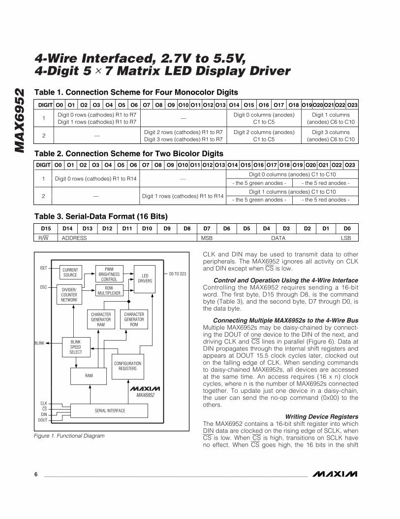
Detailed DescriptionThe MAX6952 is a serially interfaced display driver thatcan drive four digits of 5 7 cathode-row dot-matrixdisplays. The MAX6952 can drive either four monocolordigits (Table 1) or two bicolor digits (Table 2). TheMAX6952 includes a 128-character font map compris-ing 104 predefined characters and 24 user-definablecharacters. The predefined characters follow the Arialfont, with the addition of the following common sym-bols: £, €, ¥, °, µ, ±, ↑, and ↓. The 24 user-definablecharacters are uploaded by the user into on-chip RAMthrough the serial interface and are lost when thedevice is powered down. Figure 1 is the MAX6952functional diagram.
Serial InterfaceThe MAX6952 communicates through an SPI-compati-ble 4-wire serial interface. The interface has threeinputs, clock (CLK), chip select (CS), and data in (DIN),and one output, data out (DOUT). CS must be low toclock data into or out of the device, and DIN must bestable when sampled on the rising edge of CLK. DOUTis stable on the rising edge of CLK. Note that while theSPI protocol expects DOUT to be high impedancewhen the MAX6952 is not being accessed, DOUT onthe MAX6952 is never high impedance.
MA
X6
95
2
4-Wire Interfaced, 2.7V to 5.5V, 4-Digit 5 7 Matrix LED Display Driver
_______________________________________________________________________________________ 5
Pin Description
PIN
SSOP PDIPNAME FUNCTION
1, 2, 3, 6–14, 23, 24 1, 2, 3, 7–15, 26, 27 O0 to O13LED Cathode Drivers. O0 to O13 outputs sink current fromthe display’s cathode rows.
4, 5, 16 4, 5, 6, 18 GND Ground
15 17 ISETSegment Current Setting. Connect ISET to GND throughseries resistor RSET to set the peak current.
17 19 BLINK Blink Clock Output. Output is open drain.
18 20 DINSerial Data Input. Data is loaded into the internal 16-bit shiftregister on the rising edge of the CLK.
19 21 CLK
Serial-Clock Input. On the rising edge of CLK, data isshifted into the internal shift register. On the falling edge ofCLK, data is clocked out of DOUT. CLK input is active onlywhile CS is low.
20 22 DOUTSerial Data Output. Data clocked into DIN is output toDOUT 15.5 clock cycles later. Data is clocked out on therising edge of CLK. Output is push-pull.
21 23 CSChip-Select Input. Serial data is loaded into the shift registerwhile CS is low. The last 16 bits of serial data are latched onCS’s rising edge.
22 24 OSCMultiplex Clock Input. To use the internal oscillator, connectcapacitor CSET from OSC to GND. To use the externalclock, drive OSC with a 1MHz to 8MHz CMOS clock.
25–31, 34, 35, 36 28–34, 38, 39, 40 O14 to O23LED Anode Drivers. O14 to O23 outputs source current tothe display’s anode columns.
32, 33 35, 36, 37 V+Positive Supply Voltage. Bypass V+ to GND with a 47µFbulk capacitor and a 0.1µF ceramic capacitor.
MA
X6
95
2
CLK and DIN may be used to transmit data to otherperipherals. The MAX6952 ignores all activity on CLKand DIN except when CS is low.
Control and Operation Using the 4-Wire InterfaceControlling the MAX6952 requires sending a 16-bitword. The first byte, D15 through D8, is the commandbyte (Table 3), and the second byte, D7 through D0, isthe data byte.
Connecting Multiple MAX6952s to the 4-Wire BusMultiple MAX6952s may be daisy-chained by connect-ing the DOUT of one device to the DIN of the next, anddriving CLK and CS lines in parallel (Figure 6). Data atDIN propagates through the internal shift registers andappears at DOUT 15.5 clock cycles later, clocked outon the falling edge of CLK. When sending commandsto daisy-chained MAX6952s, all devices are accessedat the same time. An access requires (16 x n) clockcycles, where n is the number of MAX6952s connectedtogether. To update just one device in a daisy-chain,the user can send the no-op command (0x00) to theothers.
Writing Device Registers The MAX6952 contains a 16-bit shift register into whichDIN data are clocked on the rising edge of SCLK, whenCS is low. When CS is high, transitions on SCLK haveno effect. When CS goes high, the 16 bits in the shift
4-Wire Interfaced, 2.7V to 5.5V, 4-Digit 5 7 Matrix LED Display Driver
6 _______________________________________________________________________________________
DIGIT O0 O1 O2 O3 O4 O5 O6 O7 O8 O9 O10 O11 O12 O13 O14 O15 O16 O17 O18 O19 O20 O21 O22 O23
1Digit 0 rows (cathodes) R1 to R7Digit 1 rows (cathodes) R1 to R7
—Digit 0 columns (anodes)
C1 to C5Digit 1 columns
(anodes) C6 to C10
2 —Digit 2 rows (cathodes) R1 to R7Digit 3 rows (cathodes) R1 to R7
Digit 2 columns (anodes)C1 to C5
Digit 3 columns(anodes) C6 to C10
Table 1. Connection Scheme for Four Monocolor Digits
DIGIT O0 O1 O2 O3 O4 O5 O6 O7 O8 O9 O10 O11 O12 O13 O14 O15 O16 O17 O18 O19 O20 O21 O22 O23
Digit 0 columns (anodes) C1 to C101 Digit 0 rows (cathodes) R1 to R14 —
- the 5 green anodes - - the 5 red anodes -
Digit 1 columns (anodes) C1 to C102 — Digit 1 rows (cathodes) R1 to R14
- the 5 green anodes - - the 5 red anodes -
Table 2. Connection Scheme for Two Bicolor Digits
D15 D14 D13 D12 D11 D10 D9 D8 D7 D6 D5 D4 D3 D2 D1 D0
R/W ADDRESS MSB DATA LSB
Table 3. Serial-Data Format (16 Bits)
ISET
OSC
BLINK
CLKCS
DINDOUT
SERIAL INTERFACE
RAM
BLINKSPEEDSELECT
CONFIGURATIONREGISTERS
CHARACTERGENERATOR
ROM
CHARACTERGENERATOR
RAM
CURRENTSOURCE
DIVIDER/COUNTERNETWORK
ROWMULTIPLEXER
PWMBRIGHTNESS
CONTROLLED
DRIVERS
O0 TO O23
MAX6952
Figure 1. Functional Diagram

MA
X6
95
2
4-Wire Interfaced, 2.7V to 5.5V, 4-Digit 5 7 Matrix LED Display Driver
_______________________________________________________________________________________ 7
register are parallel loaded into a 16-bit latch. The 16bits in the latch are then decoded and executed.
The MAX6952 is writ ten to using the fol lowingsequence:
1) Take CLK low.
2) Take CS low. This enables the internal 16-bit shiftregister.
3) Clock 16 bits of data into DIN, D15 first to D0 last,observing the setup and hold times. Bit D15 is low, indicating a write command.
4) Take CS high (while CLK is still high after clockingin the last data bit).
5) Take CLK low.
Figure 3 shows a write operation when 16 bits aretransmitted.
If fewer or greater than 16 bits are clocked into theMAX6952 between taking CS low and taking CS highagain, the MAX6952 stores the last 16 bits received,including the previous transmission(s). The generalcase is when n bits (where n > 16) are transmitted tothe MAX6952. The last bits comprising bits n-15 to nare retained and are parallel loaded into the 16-bit latchas bits D15 to D0, respectively (Figure 4).
Reading Device RegistersAny register data within the MAX6952 may be read bysending a logic high to bit D15. The sequence is:
1) Take CLK low.
2) Take CS low. This enables the internal 16-bit shiftregister.
3) Clock 16 bits of data into DIN, D15 first to D0 last,observing the setup and hold times. Bit D15 is high,indicating a read command and bits D14 throughD8 contain the address of the register to read. BitsD7 to D0 contain dummy data, which is discarded.
4) Take CS high. Positions D7 through D0 in the shiftregister are now loaded with the data in the registeraddressed by bits D15 through D8. Bits
5) Take CLK low.
6) Issue another read or write command (which canbe a no-op), and examine the bit stream at DOUT;the second 8 bits are the contents of the registeraddressed by bits D14 through D8 in step 3.
Digit RegistersThe MAX6952 uses eight digit registers to store the char-acters that the user wishes to display on the four 5 7LED digits. These digit registers are implemented withtwo planes of 4 bytes, called P0 and P1. Each LED digit
is represented by 2 bytes of memory, 1 byte in plane P0and the other in plane P1. The digit registers are mappedso that a digit’s data can be updated in plane P0, orplane P1, or both planes at the same time (Table 4).
If the blink function is disabled through the Blink EnableBit E (Table 9) in the configuration register, then thedigit register data in plane P0 is used to multiplex thedisplay. The digit register data in P1 is not used. If theblink function is enabled, then the digit register data inboth plane P0 and plane P1 are alternately used to mul-tiplex the display. Blinking is achieved by multiplexingthe LED display using data planes P0 and P1 on alter-nate phases of the blink clock (Table 10).
The data in the digit registers does not control the digitsegments directly. Instead, the register data is used toaddress a character generator, which stores the data ofa 128-character font (Table 14). The lower 7 bits of thedigit data (D6 to D0) select the character from the font.The most-significant bit of the register data (D7) selectswhether the font data is used directly (D7 = 0) orwhether the font data is inverted (D7 = 1). The inversionfeature can be used to enhance the appearance ofbicolor displays by displaying, for example, a red char-acter on a green background.
Display Blink ModeThe display blinking facility, when enabled, makes thedriver flip automatically between displaying the digitregister data in planes P0 and P1. If the digit registerdata for any digit is different in the two planes, then thatdigit appears to flip between two characters. To make acharacter appear to blink on or off, write the characterto one plane, and use the blank character (0x20) for theother plane. Once blinking has been configured, it con-tinues automatically without further intervention.
Blink SpeedThe blink speed is determined by frequency of the mul-tiplex clock, OSC, and by setting the Blink RateSelection Bit B (Table 8) in the configuration register.The Blink Rate Selection Bit B sets either fast or slowblink speed for the whole display.
Initial Power-UpOn initial power-up, all control registers are reset, thedisplay is blanked, intensities are set to minimum, andshutdown is enabled (Table 5).
Configuration RegisterThe configuration register is used to enter and exitshutdown, select the blink rate, globally enable anddisable the blink function, globally clear the digit data,and reset the blink timing (Table 6).

MA
X6
95
2
4-Wire Interfaced, 2.7V to 5.5V, 4-Digit 5 7 Matrix LED Display Driver
8 _______________________________________________________________________________________
tCSS tCL tCHtCP
tCSH
tCSW
tDStDH
D15
CLK
DIN
CS
D14 D1 D0
D15
tDO
DOUT
TIMING NOT TO SCALE.
Figure 2. Timing Diagram
CS
CLK
DIN D15= 0 D14 D13 D12 D11 D10 D9 D8 D7 D6 D5 D4 D3 D2 D1 D0
DOUT D15 = 0
Figure 3. 16-Bit Write Transmission to the MAX6952
CS
CLK
DIN BIT1
BIT2
N-8 N-7 N-6 N-5 N-4 N-3 N-2 N-1
DOUT N-15
N-14 N-13 N-12 N-11 N-10 N-9 NN-15
N-31 N-30 N-29 N-28 N-27 N-26 N-25 N-24 N-23 N-22 N-21 N-20 N-19 N-18 N-17 N-16
TIMING NOT TO SCALE.
Figure 4. Transmission of More than 16 Bits to the MAX6952

MA
X6
95
2
4-Wire Interfaced, 2.7V to 5.5V, 4-Digit 5 7 Matrix LED Display Driver
_______________________________________________________________________________________ 9
ADDRESS (COMMAND BYTE)REGISTER
D15 D14 D13 D12 D11 D10 D9 D8
HEXCODE
No-Op R/W 0 0 0 0 0 0 0 0x00
Intensity10 R/W 0 0 0 0 0 0 1 0x01
Intensity32 R/W 0 0 0 0 0 1 0 0x02
Scan-Limit R/W 0 0 0 0 0 1 1 0x03
Configuration R/W 0 0 0 0 1 0 0 0x04
User-Defined Fonts R/W 0 0 0 0 1 0 1 0x05
Factory reserved. Do not write to this. R/W 0 0 0 0 1 1 0 0x06
Display Test R/W 0 0 0 0 1 1 1 0x07
Digit 0 Plane P0 R/W 0 1 0 0 0 0 0 0x20
Digit 1 Plane P0 R/W 0 1 0 0 0 0 1 0x21
Digit 2 Plane P0 R/W 0 1 0 0 0 1 0 0x22
Digit 3 Plane P0 R/W 0 1 0 0 0 1 1 0x23
Digit 0 Plane P1 R/W 1 0 0 0 0 0 0 0x40
Digit 1 Plane P1 R/W 1 0 0 0 0 0 1 0x41
Digit 2 Plane P1 R/W 1 0 0 0 0 1 0 0x42
Digit 3 Plane P1 R/W 1 0 0 0 0 1 1 0x43
Write Digit 0 Plane P0 and Plane P1 withSame Data (Reads as 0x00)
R/W 1 1 0 0 0 0 0 0x60
Write Digit 1 Plane P0 and Plane P1 withSame Data (Reads as 0x00) R/W 1 1 0 0 0 0 1 0x61
Write Digit 2 Plane P0 and Plane P1 withSame Data (Reads as 0x00)
R/W 1 1 0 0 0 1 0 0x62
Write Digit 3 Plane P0 and Plane P1 withSame Data (Reads as 0x00)
R/W 1 1 0 0 0 1 1 0x63
Table 4. Register Address Map
MA
X6
95
2
4-Wire Interfaced, 2.7V to 5.5V, 4-Digit 5 7 Matrix LED Display Driver
10 ______________________________________________________________________________________
Shutdown Mode (S Data Bit D0) FormatThe S bit in the configuration register selects shutdownor normal operation (Table 7). The display driver can beprogrammed while in shutdown mode, and shutdownmode is overridden when in display test mode. For nor-mal operation, the S bit should be set to 1.
Blink Rate Selection (B Data Bit D2) FormatThe B bit in the configuration register selects the blinkrate. This is the speed that the segments alternate
between plane P0 and plane P1 refresh data. The blinkrate is determined by the frequency of the multiplex clockOSC, in addition to the setting of the B bit (Table 8).
Global Blink Enable/Disable(E Data Bit D3) Format
The E bit globally enables or disables the blink featureof the device (Table 9). When blink is globally enabled,then the digit data in both planes P0 and P1 are usedto control the display (Table 10).
REGISTER DATAREGISTER POWER-UP CONDITION
ADDRESSCODE (HEX) D7 D6 D5 D4 D3 D2 D1 D0
Intensity10 1/16 (min on) 0x01 0 0 0 0 0 0 0 0
Intensity32 1/16 (min on) 0x02 0 0 0 0 0 0 0 0
Scan Limit Display 4 digits: 0 1 2 3 0x03 X X X X X X X 1
ConfigurationShutdown enabled,blink speed is slow,
blink disabled0x04 0 X 0 0 0 0 X 0
User-Defined FontAddress Pointer
Address 0x80; pointing tothe first user-defined font
location0x05 1 0 0 0 0 0 0 0
Display Test Normal operation 0x07 X X X X X X X 0
Digit 0 Plane P0 Blank digit (0x20) 0x20 0 0 1 0 0 0 0 0
Digit 1 Plane P0 Blank digit (0x20) 0x21 0 0 1 0 0 0 0 0
Digit 2 Plane P0 Blank digit (0x20) 0x22 0 0 1 0 0 0 0 0
Digit 3 Plane P0 Blank digit (0x20) 0x23 0 0 1 0 0 0 0 0
Digit 0 Plane P1 Blank digit (0x20) 0x40 0 0 1 0 0 0 0 0
Digit 1 Plane P1 Blank digit (0x20) 0x41 0 0 1 0 0 0 0 0
Digit 2 Plane P1 Blank digit (0x20) 0x42 0 0 1 0 0 0 0 0
Digit 3 Plane P1 Blank digit (0x20) 0x43 0 0 1 0 0 0 0 0
Table 5. Initial Power-Up Register Status
REGISTER DATAREGISTER
D7 D6 D5 D4 D3 D2 D1 D0
ConfigurationRegister
P X R T E B X S
Table 6. Configuration Register FormatREGISTER DATA
MODED7 D6 D5 D4 D3 D2 D1 D0
ShutdownMode
P X R T E B X 0
NormalOperation
P X R T E B X 1
Table 7. Shutdown Control (S Data Bit D0)Format

MA
X6
95
2
4-Wire Interfaced, 2.7V to 5.5V, 4-Digit 5 7 Matrix LED Display Driver
______________________________________________________________________________________ 11
MAX6952
DOUT
MICROCONTROLLERCLK
DIN
MAX6952 MAX6952CLK
DIN
CS
DOUT
CLK
DIN
CS
DOUT
CLK
DIN
CS
DOUT
CS
Figure 6. MAX6952 Daisy-Chain Connection
REGISTER DATAMODE
D7 D6 D5 D4 D3 D2 D1 D0
Slow blinking (Segments are refreshed using plane P0 for 1s, plane P1for 1s, for OSC = 4MHz.)
P X R T E 0 X S
Table 8. Blink Rate Selection (B Data Bit D2) Format
REGISTER DATAMODE
D7 D6 D5 D4 D3 D2 D1 D0
Blink function is disabled. P X R T 0 B X S
Blink function is enabled. P X R T 1 B X S
Table 9. Global Blink Enable/Disable (E Data Bit D3) Format
When blink is globally disabled, then only the digit datain plane P0 is used to control the display. The digit datain plane P1 is ignored.
Global Blink Timing Synchronization(T Data Bit D4) Format
By setting the T bit in multiple MAX6952s at the sametime (or in quick succession), the blink timing can besynchronized across all the devices (Table 11). Notethat the display multiplexing sequence is also reset,which might give rise to a one-time display flicker whenthe register is written.
Global Clear Digit Data (R Data Bit D5) FormatWhen global digit data clear is set, the digit data for bothplanes P0 and P1 for all digits is cleared (Table 12).
Blink Phase Readback (P Data Bit D7) FormatWhen the configuration register is read, the P bitreflects the state of the blink output pin at that time(Table 13).
Character Generator Font MappingThe font is a 5 7 matrix comprising 104 characters inROM, and 24 user-definable characters. The selectionfrom the total of 128 characters is represented by thelower 7 bits of the 8-bit digit registers. The most-signifi-cant bit, shown as x in the ROM map below, is zero tolight LEDs as shown by the black segments in Table14, and 1 to display the inverse.
The character map follows the Arial font for 96 charac-ters in the x0101000 through x1111111 range. The first

MA
X6
95
2
4-Wire Interfaced, 2.7V to 5.5V, 4-Digit 5 7 Matrix LED Display Driver
12 ______________________________________________________________________________________
32 characters map the 24 user-definable positions(RAM00 to RAM23), plus eight extra common charac-ters in ROM.
User-Defined FontsThe 24 user-definable characters are represented by120 entries of 7-bit data, five entries per character, andare stored in the MAX6952's internal RAM.
The 120 user-definable font data entries are written andread through a single register, address 0x05. Anautoincrementing font address pointer in the MAX6952
indirectly accesses the font data. The font addresspointer can be written, setting one of 120 addressesbetween 0x00 and 0xF7, but cannot be read back. Thefont data is written to and read from the MAX6952 indi-rectly, using this font address pointer. Unused fontlocations can be used as general-purpose scratchRAM, bearing in mind that the font registers are only 7bits wide, not 8.
Table 15 shows how the single user-defined font regis-ter 0x05 is used to set the font address pointer, writefont data, and read font data. A read action alwaysreturns font data from the font address pointer position.A write action sets the 7-bit font address pointer if theMSB is set, or writes 7-bit font data to the font addresspointer position if the MSB is clear.
The font address pointer autoincrements after a validaccess to the user-definable font data. Auto-incrementing allows the 120 font data entries to be writ-ten and read back very quickly because the font point-er address need only be set once. When the last datalocation 0xF7 is written, the font address pointer autoin-crements to address 0x80. If the font address pointer isset to an out-of-range address by writing data in the0xF8 to 0xFF range, then address 0x80 is set instead(Table 16).
Table 17 shows the user-definable font pointer baseaddresses.
SEGMENT’SBIT SETTINGIN PLANE P1
SEGMENT’SBIT SETTINGIN PLANE P0
SEGMENTBEHAVIOR
0 0 Segment off
0 1Segment on only duringthe 1st half of each blinkperiod
1 0Segment on only duringthe 2nd half of eachblink period
1 1 Segment on
Table 10. Digit Register Mapping withBlink Globally Enabled
REGISTER DATAMODE
D7 D6 D5 D4 D3 D2 D1 D0
Blink timing counters are unaffected. P X R 0 E B X S
Blink timing counters are reset on the rising edge of CS. P X R 1 E B X S
Table 11. Global Blink Timing Synchronization (T Data Bit D4) Format
REGISTER DATAMODE
D7 D6 D5 D4 D3 D2 D1 D0
Digit data for both planes P0 and P1 are unaffected. P X 0 T E B X S
Digit data for both planes P0 and P1 are cleared on therising edge of CS.
P X 1 T E B X S
Table 12. Global Clear Digit Data (R Data Bit D5) Format
REGISTER DATAMODE
D7 D6 D5 D4 D3 D2 D1 D0
P1 Blink Phase 0 X R T E B X S
P0 Blink Phase 1 X R T E B X S
Table 13. Blink Phase Readback (P Data Bit D7) Format

MA
X6
95
2
4-Wire Interfaced, 2.7V to 5.5V, 4-Digit 5 7 Matrix LED Display Driver
______________________________________________________________________________________ 13
Table 18 shows an example of data (characters 0, 1,and 2) being stored in the first three user-defined fontlocations, illustrating the orientation of the data bits.
Table 19 shows the six sequential write commandsrequired to set a MAX6953's font character RAM02 withthe data to display character 2 given in the font RAMillustration above.
Multiplex Clock and Blink TimingThe OSC pin can be fitted with capacitor CSET to GND(to use the internal RC multiplex oscillator), or driven byan external clock. The multiplex clock frequency deter-mines the multiplex scan rate and the blink timing. Thedisplay scan rate is calculated by dividing the frequencyat OSC by 5600. With OSC at 4 MHz, each display digitis enabled for 100µs and the display scan rate is714.29Hz.
The on-chip oscillator may be accurate enough forapplications using a single device. If an exact blink rateis required, use an external clock ranging between1MHz and 8MHz to drive OSC. The OSC inputs of multi-ple MAX6952s can be tied together to a common exter-nal clock to make the devices blink at the same rate.The relative blink phasing of multiple MAX6952s can besynchronized by setting the T bit in the control registerfor all the devices in quick succession (Table 11).
If the serial interfaces of multiple MAX6952s are daisy-chained by connecting DOUT of one device to DIN ofthe next, then synchronization is achieved automaticallyby updating the control register for all devices together.For MAX6952s, the devices can be synchronized bytransmitting the serial data for the control register, andthen toggling the CS pin for each device, either togeth-er or in quick succession. Figure 7 is the multiplex tim-ing diagram.
Blink Output The blink output indicates the blink phase, and is highduring the P0 period and low during the P1 period.Blink phase status can also be read back as the P bit inthe configuration register (Table 13). Typical uses forthis output are:
• To provide an interrupt to the processor so that seg-ment data can be changed synchronous to theblinking. For example, a clock application may havecolon segments blinking every second betweenhours and minute digits, and the minute display isbest changed in step with the colon segments. Also,if the rising edge of blink is detected, there is half ablink period to change the P1 digit data. Similarly, ifthe falling edge of blink is detected, the user hashalf a blink period to change the P0 digit data.
0000
0001
0010
0011
0100
0101
0110
0111
1000
1001
1010
1011
1100
1101
1110
1111
x000 x001 x010 x011 x100 x101 x110 x111
RAM00
RAM01
RAM02
RAM03
RAM04
RAM05
RAM06
RAM07
MSB
LSB
RAM08
RAM09
RAM10
RAM11
RAM12
RAM13
RAM14
RAM15
RAM16
RAM17
RAM18
RAM19
RAM20
RAM21
RAM22
RAM23
Table 14. Character Map
MA
X6
95
2
4-Wire Interfaced, 2.7V to 5.5V, 4-Digit 5 7 Matrix LED Display Driver
14 ______________________________________________________________________________________
• If OSC is driven with an accurate frequency, blinkcan be used as a seconds counter or similar.
Scan-Limit RegisterThe scan-limit register sets how many monocolor digitsare displayed, either two or four. A bicolor digit is con-nected as two monocolor digits.
The multiplexing scheme drives digits 0 and 1 at thesame time, then digits 2 and 3 at the same time. Toincrease the effective brightness of the displays, driveonly two digits instead of four. By doing this, the aver-age segment current doubles, but also doubles thenumber of MAX6952s required to drive a given numberof digits.
Because digit 1 is driven at the same time as digit 0(and digit 3 is driven at the same time as digit 2), only 1bit is used to set the scan limit. The bit is clear if one ortwo digits are to be driven, and set if three or four digitsare to be driven (Table 20). Change the scan-limit register only when the MAX6952 is in shutdown mode.
Intensity RegistersDisplay brightness is controlled digitally by four pulse-width modulators, one for each display digit. Each digit iscontrolled by a nibble of one of the two intensity registers,Intensity10 and Intensity32. The modulator scales theaverage segment current in 16 steps from a maximum of15/16 down to 1/16 of the peak current. The minimuminterdigit blanking time is, therefore, 1/16 of a cycle. Themaximum duty cycle is 15/16. (Tables 21 and 22).
No-Op RegisterA write to the no-op register is ignored.
Selecting External Components RSET andCSET to Set Oscillator Frequency and
Segment CurrentThe RC oscillator uses an external resistor RSET and anexternal capacitor CSET to set the oscillator frequency,fOSC. The allowed range of fOSC is 1MHz to 8MHz.RSET also sets the peak segment current. The recom-mended values of RSET and CSET set the oscillator to4MHz, which makes the blink frequencies 0.5Hz and1Hz. The recommended value of RSET also sets thepeak current to 40mA, which makes the segment cur-rent adjustable from 2.5mA to 37.5mA in 2.5mA steps:
ISEG = KI / RSET mA
fOSC = KF / (RSET CSET + CSTRAY) MHz
Where:
KI = 2144
KF = 6000
RSET = external resistor in kΩCSET = external capacitor in pF
CSTRAY = stray capacitance from OSC pin to GND inpF, typically 2pF
The recommended value of RSET is 53.6kΩ and therecommended value of CSET is 26pF.
ADDRESS CODE(HEX)
REGISTERDATA
SPI READOR WRITE
FUNCTION
0x85 0x00–0x7F ReadRead 7-bit user-definable font data entry from current fontaddress. MSB of the register data is clear. Font addresspointer is incremented after the read.
0x05 0x00–0x7F WriteWrite 7-bit user-definable font data entry to current fontaddress. Font address pointer is incremented after thewrite.
0x05 0x80–0xFF Write Write font address pointer with the register data.
Table 15. Memory Mapping of User-Defined Font Register 0x05
FONT POINTER ADDRESS ACTION
0x80 to 0xF6Valid range to set the font address pointer. Pointer autoincrements after a font data read orwrite, while pointer address remains in this range.
0xF7 Font address resets to 0x80 after a font data read or write to this pointer address.
0xF8 to 0xFF Invalid range to set the font address pointer. Pointer is set to 0x80 if address.
Table 16. Font Pointer Address Behavior

MA
X6
95
2
4-Wire Interfaced, 2.7V to 5.5V, 4-Digit 5 7 Matrix LED Display Driver
______________________________________________________________________________________ 15
REGISTER DATAFONTCHARACTER
ADDRESSCODE (HEX)
REGISTERDATA (HEX)
D7 D6 D5 D4 D3 D2 D1 D0
RAM00 0x05 0x80 1 0 0 0 0 0 0 0
RAM01 0x05 0x85 1 0 0 0 0 1 0 1
RAM02 0x05 0x8A 1 0 0 0 1 0 1 0
RAM03 0x05 0x8F 1 0 0 0 1 1 1 1
RAM04 0x05 0x94 1 0 0 1 0 1 0 0
RAM05 0x05 0x99 1 0 0 1 1 0 0 1
RAM06 0x05 0x9E 1 0 0 1 1 1 1 0
RAM07 0x05 0xA3 1 0 1 0 0 0 1 1
RAM08 0x05 0xA8 1 0 1 0 1 0 0 0
RAM09 0x05 0xAD 1 0 1 0 1 1 0 1
RAM10 0x05 0xB2 1 0 1 1 0 0 1 0
RAM11 0x05 0xB7 1 0 1 1 0 1 1 1
RAM12 0x05 0xBC 1 0 1 1 1 1 0 0
RAM13 0x05 0xC1 1 1 0 0 0 0 0 1
RAM14 0x05 0xC6 1 1 0 0 0 1 1 0
RAM15 0x05 0xCB 1 1 0 0 1 0 1 1
RAM16 0x05 0xD0 1 1 0 1 0 0 0 0
RAM17 0x05 0xD5 1 1 0 1 0 1 0 1
RAM18 0x05 0xDA 1 1 0 1 1 0 1 0
RAM19 0x05 0xDF 1 1 0 1 1 1 1 1
RAM20 0x05 0xE4 1 1 1 0 0 1 0 0
RAM21 0x05 0xE9 1 1 1 0 1 0 0 1
RAM22 0x05 0xEE 1 1 1 0 1 1 1 0
RAM23 0x05 0xF3 1 1 1 1 0 0 1 1
Table 17. User-Definable Font Pointer Base Address Table
The recommended value of RSET is the minimumallowed value since it sets the display driver to themaximum allowed segment current. RSET can be set toa higher value to set the segment current to a lowerpeak value where desired. The user must also ensurethat the peak current specifications of the LEDs con-nected to the driver are not exceeded.
The effective value of CSET includes not only the actualexternal capacitor used, but also the stray capacitancefrom OSC to GND. This capacitance is usually in the1pF to 5pF range, depending on the layout used.
Display-Test RegisterThe display-test register switches the drivers betweenone of two modes: normal and display test. Display-testmode turns all LEDs on by overriding, but not altering,all control and digit registers (including the shutdown
register). In display-test mode, eight digits are scannedand the duty cycle is 7/16 (half power). Table 23 liststhe display-test register format.
Applications InformationChoosing Supply Voltage to Minimize
Power DissipationThe MAX6952 drives a peak current of 40mA into LEDswith a 2.4V forward-voltage drop when operated from asupply voltage of at least 3.0V. The minimum voltagedrop across the internal LED drivers is, therefore (3.0V -2.4V) = 0.6V. If a higher supply voltage is used, the dri-ver absorbs a higher voltage, and the driver’s powerdissipation increases accordingly. However, if the LEDsused have a higher forward voltage drop than 2.4V, thesupply voltage must be raised accordingly to ensurethat the driver always has at least 0.6V headroom.

MA
X6
95
2
4-Wire Interfaced, 2.7V to 5.5V, 4-Digit 5 7 Matrix LED Display Driver
16 ______________________________________________________________________________________
REGISTER DATAFONTCHARACTER
FONTADDRESSPOINTER
ADDRESSCODE (HEX)
FONTPOINTERADDRESS
(HEX) D7 D6 D5 D4 D3 D2 D1 D0
RAM00 0x00 0x05 0x80 0 0 1 1 1 1 1 0
RAM00 0x01 0x05 0x81 0 1 0 1 0 0 0 1
RAM00 0x02 0x05 0x82 0 1 0 0 1 0 0 1
RAM00 0x03 0x05 0x83 0 1 0 0 0 1 0 1
RAM00 0x04 0x05 0x84 0 0 1 1 1 1 1 0
RAM01 0x05 0x05 0x85 0 0 0 0 0 0 0 0
RAM01 0x06 0x05 0x86 0 1 0 0 0 0 1 0
RAM01 0x07 0x05 0x87 0 1 1 1 1 1 1 1
RAM01 0x08 0x05 0x88 0 1 0 0 0 0 0 0
RAM01 0x09 0x05 0x89 0 0 0 0 0 0 0 0
RAM02 0x0A 0x05 0x8A 0 1 0 0 0 0 1 0
RAM02 0x0B 0x05 0x8B 0 1 1 0 0 0 0 1
RAM02 0x0C 0x05 0x8C 0 1 0 1 0 0 0 1
RAM02 0x0D 0x05 0x8D 0 1 0 0 1 0 0 1
RAM02 0x0E 0x05 0x8E 0 1 0 0 0 1 1 0
Table 18. User-Definable Character Storage Example
ADDRESS CODE(HEX)
REGISTER DATA(HEX)
ACTION BEING PERFORMED
0x05 0x8A Set font address pointer to the base address of font character RAM02.
0x05 0x421st 7 bits of data: 1000010 goes to font address 0x8A; pointer then autoincrementsto address 0x8B.
0x05 0x612nd 7 bits of data: 1100001 goes to font address 0x8B; pointer thenautoincrements to address 0x8C.
0x05 0x513rd 7 bits of data: 1010001 goes to font address 0x8C; pointer thenautoincrements to address 0x8D.
0x05 0x494th 7 bits of data: 1001001 goes to font address 0x8D; pointer thenautoincrements to address 0x8E.
0x05 0x465th 7 bits of data: 1000110 goes to font address 0x8E; pointer then autoincrementsto address 0x8F.
Table 19. Setting a Font Character to RAM Example
REGISTER DATASCANLIMIT
ADDRESSCODE (HEX)
D7 D6 D5 D4 D3 D2 D1 D0
HEXCODE
Display digits 0 and 1 only 0x03 X X X X X X X 0 0xX0
Display digits 0, 1, 2, and 3 0x03 X X X X X X X 1 0xX1
Table 20. Scan Limit Register Format

MA
X6
95
2
4-Wire Interfaced, 2.7V to 5.5V, 4-Digit 5 7 Matrix LED Display Driver
______________________________________________________________________________________ 17
DUTY CYCLETYPICAL SEGMENT
CURRENT (mA)ADDRESS
CODE (HEX)D7 D6 D5 D4 D3 D2 D1 D0
HEXCODE
1/16 (min on) 2.5 0x01, 0x02 0 0 0 0 0xX02/16 5 0x01, 0x02 0 0 0 1 0xX1
3/16 7.5 0x01, 0x02 0 0 1 0 0xX24/16 10 0x01, 0x02 0 0 1 1 0xX3
5/16 12.5 0x01, 0x02 0 1 0 0 0xX46/16 15 0x01, 0x02 0 1 0 1 0xX5
7/16 17.5 0x01, 0x02 See Table 22. 0 1 1 0 0xX68/16 20 0x01, 0x02 0 1 1 1 0xX7
9/16 22.5 0x01, 0x02 1 0 0 0 0xX810/16 25 0x01, 0x02 1 0 0 1 0xX911/16 27.5 0x01, 0x02 1 0 1 0 0xXA
12/16 30 0x01, 0x02 1 0 1 1 0xXB13/16 32.5 0x01, 0x02 1 1 0 0 0xXC
14/16 35 0x01, 0x02 1 1 0 1 0xXD15/16 37.5 0x01, 0x02 1 1 1 0 0xXE
15/16 (max on) 37.5 0x01, 0x02 1 1 1 1 0xXF
Table 21. Intensity Register Format for Digit 0 (Address 0x01) and Digit 2 (Address 0x02)
DUTYCYCLE
TYPICALSEGMENT
CURRENT (mA)
ADDRESSCODE (HEX)
D7 D6 D5 D4 D3 D2 D1 D0HEX
CODE
1/16 (min on) 2.5 0x01, 0x02 0 0 0 0 0x0X2/16 5 0x01, 0x02 0 0 0 1 0x1X
3/16 7.5 0x01, 0x02 0 0 1 0 0x2X4/16 10 0x01, 0x02 0 0 1 1 0x3X
5/16 12.5 0x01, 0x02 0 1 0 0 0x4X6/16 15 0x01, 0x02 0 1 0 1 0x5X
7/16 17.5 0x01, 0x02 0 1 1 0 0x6X8/16 20 0x01, 0x02 0 1 1 1 See Table 21. 0x7X
9/16 22.5 0x01, 0x02 1 0 0 0 0x8X10/16 25 0x01, 0x02 1 0 0 1 0x9X
11/16 27.5 0x01, 0x02 1 0 1 0 0xAX12/16 30 0x01, 0x02 1 0 1 1 0xBX
13/16 32.5 0x01, 0x02 1 1 0 0 0xCX14/16 35 0x01, 0x02 1 1 0 1 0xDX15/16 37.5 0x01, 0x02 1 1 1 0 0xEX
15/16 (max on) 37.5 0x01, 0x02 1 1 1 1 0xFX
Table 22. Intensity Register Format for Digit 1 (Address 0x01) and Digit 3 (Address 0x02)

MA
X6
95
2
4-Wire Interfaced, 2.7V to 5.5V, 4-Digit 5 7 Matrix LED Display Driver
18 ______________________________________________________________________________________
REGISTER DATA
MODEADDRESS
CODE (HEX) D7 D6 D5 D4 D3 D2 D1 D0
Normal operation 0x07 X X X X X X X 0
Display test 0x07 X X X X X X X 1
Table 23. Display-Test Register Format
The voltage drop across the drivers with a nominal 5Vsupply (5.0V - 2.4V) = 2.6V is nearly 3 times the dropacross the drivers with a nominal 3.3V supply (3.3V -2.4V) = 0.9V. In most systems, consumption is animportant design criterion, and the MAX6952 should beoperated from the system’s 3.3V nominal supply. Inother designs, the lowest supply voltage may be 5V.The issue now is to ensure the dissipation limit for theMAX6952 is not exceeded. This can be achieved byinserting a series resistor in the supply to the MAX6952,ensuring that the supply decoupling capacitors are stillon the MAX6952 side of the resistor. For example, con-sider the requirement that the minimum supply voltageto a MAX6952 must be 3.0V, and the input supplyrange is 5V ±5%.
Maximum supply current is:12mA + (40mA x 10) = 412mA
Minimum input supply voltage is 4.75V.
Maximum series resistor value is:(4.75V - 3.0V) / 0.412A = 4.25Ω
We choose 3.3Ω ±5%. Worst-case resistor dissipationis at maximum toleranced resistance, i.e., (0.412A) 2 x(3.3Ω 1.05) = 0.577W. We choose a 1W resistor rat-ing. The maximum MAX6952 supply voltage is at maxi-mum input supply voltage and minimum tolerancedresistance, i.e., 5.25V - (0.412A x 3.3Ω 0.95) = 3.97V.
Low-Voltage OperationThe MAX6952 works over the 2.7V to 5.5V supplyrange. The minimum useful supply voltage is deter-mined by the forward voltage drop of the LEDs at thepeak current ISEG, plus the 0.6V headroom required bythe driver output stages. The MAX6952 correctly regu-lates ISEG with a supply voltage above this minimumvoltage. If the supply drops below this minimum volt-age, the driver output stages may brown out, and beunable to regulate the current correctly. As the supplyvoltage drops further, the LED segment drive currentbecomes effectively limited by the output driver's on-resistance, and the LED drive current drops. The char-acteristics of each individual LED in a 5 7 matrix digitare well matched, so the result is that the display inten-
sity dims uniformly as supply voltage drops out of regu-lation and beyond. The MAX6952 operates down to2.5V supply voltage (although most displays are verydim at this voltage), provided that the MAX6952 is pow-ered up initially to at least 2.7V to trigger the device'sinternal reset.
Computing Power DissipationThe upper limit for power dissipation (PD) for theMAX6952 is determined from the following equation:
PD = (V+ 12mA) + (V+ - VLED) (DUTY x ISEG N)
where:
V+ = supply voltage
Duty = duty cycle set by intensity register
N = number of segments driven (worst case is 10)
VLED = LED forward voltage
ISEG = segment current set by RSET
PD = power dissipation, in mW if currents are in mA
Dissipation example:
ISEG = 40mA, N = 10, Duty = 15 / 16, VLED = 2.4V at 40mA, V+ = 3.6V
PD = 3.6V (12mA) + (3.6V - 2.4V)(15 / 16 40mA 10)= 0.493W
Thus, for a 36-pin SSOP package (TJA = 1 / 0.0118 =+85°C/W from operating ratings), the maximum allowedambient temperature TA is given by:
TJ(MAX) = TA + (PD TJA) = +150°C = TA + (0.493 +85°C/W)
So, TA = +108°C. Thus, the part can be operated safelyat a maximum package temperature of +85°C.
Power SuppliesThe MAX6952 operates from a single 2.7V to 5.5Vpower supply. Bypass the power supply to GND with a0.1µF capacitor as close to the device as possible. Adda 47µF capacitor if the MAX6952 is not close to theboard’s input bulk decoupling capacitor.

MA
X6
95
2
4-Wire Interfaced, 2.7V to 5.5V, 4-Digit 5 7 Matrix LED Display Driver
______________________________________________________________________________________ 19
DIGIT 1ROW 1
DIGIT 1ROW 2
DIGIT 1ROW 3
DIGIT 1ROW 4
DIGIT 1ROW 5
DIGIT 1ROW 6
DIGIT 1ROW 7
DIGIT 3ROW 1
DIGIT 3ROW 2
DIGIT 3ROW 3
DIGIT 3ROW 4
DIGIT 3ROW 5
DIGIT 3ROW 6
DIGIT 3ROW 7
DIGIT 1ROW 1
COLUMN DRIVERPINS O19-O23
DIGIT 0ROW 1
DIGIT 0ROW 2
DIGIT 0ROW 3
DIGIT 0ROW 4
DIGIT 0ROW 5
DIGIT 0ROW 6
DIGIT 0ROW 7
DIGIT 2ROW 1
DIGIT 2ROW 2
DIGIT 2ROW 3
DIGIT 2ROW 4
DIGIT 2ROW 5
DIGIT 2ROW 6
DIGIT 2ROW 7
DIGIT 0ROW 1
COLUMN DRIVERPINS O14-O18
DIGIT 1 ROW 1’s 100µs MULTIPLEX TIMESLOTCURRENT SOURCE
1/16TH
2/16TH
(MIN ON)
3/16TH
4/16TH
5/16TH
6/16TH
7/16TH
8/16TH
9/16TH
10/16TH
11/16TH
12/16TH
13/16TH
14/16TH
15/16TH
16/16TH
(MAX ON)
CURRENT SOURCE
CURRENT SOURCE
CURRENT SOURCE
CURRENT SOURCE
CURRENT SOURCE
CURRENT SOURCE
CURRENT SOURCE
CURRENT SOURCE
CURRENT SOURCE
CURRENT SOURCE
CURRENT SOURCE
CURRENT SOURCE
CURRENT SOURCE
CURRENT SOURCE
CURRENT SOURCE
ONE COMPLETE 1.4ms MULTIPLEX CYCLE AROUND 14 ROWS
100µs
DIGIT 1 COLUMNDRIVER OUTPUTS
PINS O19-O23
HIGH-Z
HIGH-Z
HIGH-Z
HIGH-Z
HIGH-Z
HIGH-Z
HIGH-Z
HIGH-Z
HIGH-Z
HIGH-Z
HIGH-Z
HIGH-Z
HIGH-Z
HIGH-Z
HIGH-Z
HIGH-Z
DIGITS 0 & 1ROW OUTPUTS
PINS O0–O6
HIGH-Z
LOW
DIGITS 2 & 3ROW OUTPUTS
PINS O7–O13
HIGH-Z HIGH-Z
HIGH-ZMINIMUM 6.25µs INTERDIGIT BLANKING INTERVAL
START OFNEXT CYCLE
Figure 7. Multiplex Timing Diagram (OSC = 4MHz)

Pin Configurations
40 O23
O22
O21
V+
V+
V+
O20
O19
O18
O17
O16
O15
O14
O13
O12
N.C.
OSC
DOUT
CLK
39
38
37
36
35
34
33
32
31
1
2
3
4
5
6
7
8
9
10
O0
O1
O2
GND
GND
GND
O3
O4
O5
O6
O7
O8
O9
O10
O11
N.C.
ISET
GND
BLINK
DIN
TOP VIEW
MAX695230
29
28
27
26
25
24
23
22
21
11
12
13
14
15
16
17
18
19
PDIP
20
36
35
34
33
32
31
30
29
28
27
26
25
24
23
1
2
3
4
5
6
7
8
9
10
11
12
13
14
O23
O22
O21
V+
V+
O20
O12
O19
O18
O17
O16
O15
O14
O13
O11
O10
O9
O8
O7
O6
O5
O4
O3
GND
GND
O2
O1
O0
SSOP
MAX6952
22
21
20
19
15
16
17
18 CLK
OSC
DOUT
DIN
BLINK
GND
ISET
CS
CS
MA
X6
95
2
4-Wire Interfaced, 2.7V to 5.5V, 4-Digit 5 7 Matrix LED Display Driver
20 ______________________________________________________________________________________
Board LayoutWhen designing a board, use the following guidelines:
1) The RSET connection to the ISET pin is a high-imped-ance node, and sensitive to layout. Place RSET rightnext to the ISET pin and route RSET directly to thesepins with very short tracks.
2) Ensure that the track from the ground end of RSETroutes directly to GND pin 18 (PDIP package) orGND pin 16 (SSOP package), and that this track isnot used as part of any other ground connection.
Chip InformationTRANSISTOR COUNT: 43,086
PROCESS: CMOS

MA
X6
95
2
4-Wire Interfaced, 2.7V to 5.5V, 4-Digit 5 7 Matrix LED Display Driver
Maxim cannot assume responsibility for use of any circuitry other than circuitry entirely embodied in a Maxim product. No circuit patent licenses areimplied. Maxim reserves the right to change the circuitry and specifications without notice at any time.
21 ____________________Maxim Integrated Products, 120 San Gabriel Drive, Sunnyvale, CA 94086 408-737-7600
© 2002 Maxim Integrated Products Printed USA is a registered trademark of Maxim Integrated Products.
SS
OP
.EP
S
PACKAGE OUTLINE, 36L SSOP, 0.80 MM PITCH
11
21-0040 EREV.DOCUMENT CONTROL NO.APPROVAL
PROPRIETARY INFORMATION
TITLE:
FRONT VIEW
MAX
0.0110.104
0.017
0.299
0.013
INCHES
0.291
0.009
E
C
DIM
0.0120.004
BA1
MIN0.096A
0.23
7.40 7.60
0.32
MILLIMETERS
0.100.30
2.44MIN
0.440.29
MAX
2.65
0.0400.020L 0.51 1.02
H 0.4140.398 10.11 10.51
e 0.0315 BSC 0.80 BSC
D 0.6120.598 15.20 15.55
HE
A1 A
D
eB 0 -8
L
C
TOP VIEW
SIDE VIEW
1
36
Package Information(The package drawing(s) in this data sheet may not reflect the most current specifications. For the latest package outline information,go to www.maxim-ic.com/packages.)