evaluation of laminates in pb-free hasl process and pb ... · evaluation of laminates in pb-free...
TRANSCRIPT

Evaluation of Laminates in Pb-free HASL Process and Pb-free Assembly
Environment
Khaw Mei Ming, Andrey Lee
Agilent Technologies
Bayan Lepas, Malaysia
Abstract
An evaluation of four FR4 laminates in commonly used stack-ups was done to determine their survivability for the Pb-free
HASL process followed by a worst case Pb-free manufacturing environment of 6 X reflow @ 260°C and 1 X wave @ 270°C.
The work also includes a laminate compatibility study in a Pb-free hot air solder leveling (HASL) profile.
Introduction
This project evaluated four different FR4 low cost laminates that were recommended by various PCB suppliers or are in
niche uses. Pb-free HASL process was added to give an additional environmental stress and further evaluation of vertical
and horizontal Pb-free HASL processes. The test vehicles consist of 4 different materials, 2 different layer counts each, 4
different surface finishes and 2 different resin contents. Results include visual inspection of the materials after 1X vertical
Pb-free HASL, 6X Pb-free reflow and 1X Pb-free wave, connectivity testing after each thermal cycle and scanning acoustic
microscopy (SAM) scans. Cross-section work is still to be performed on selected locations where voids or delamination were
detected on the board during SAM.
This paper focuses on 2 main evaluations. DOE1 studies the vertical Pb-free HASL thermal profiling in comparison to the
tin lead HASL profiles at the PCB fabricators. DOE2 focuses on the survivability of the test vehicles through the Pb-free
HASL plating process and a worst case Pb-free manufacturing environment.
DOE1 Vertical Pb-free HASL Thermal Profile
The objective of this design of experiments is to compare internal and surface temperatures of 2 PCB materials during the
HASL dipping process in tin lead and Pb-free nickel-doped tin-copper (SnCuNi) solder alloy. The board features are as
detailed below.
Test vehicle size: 11” x 11”
Layer count: 10
Overall board thickness: 1.9mm
Board material (A1, A2, B): High Tg laminate
Table 1: DOE1 Test Condition
Laminate A1 in SnPb Laminate A2 in SnCuNi Laminate B in SnCuNi
Solder Temperature, °C 260 265 265
Dipping Time, sec 7 7 5
Note: No Air Knife was used during the evaluation.
Thermocouples 1, 3 and 5 (blue squares) were secured on the PCB surface, whereas thermocouples 2, 4 and 6 (red circles)
were embedded into the center of the internal PCB stack-up, all with high temperature wires and epoxy.
Figure 1: Thermocouple Locations Fig. 2: Thermocouples mounted on the profile board
As originally published in the IPC APEX EXPO Proceedings.

DOE2: Extreme Pb-free Assembly Process Survivability
This DOE evaluates the survivability of various combinations of surface finishes with 4 different types of laminates through
the Pb-free HASL process (for HASL plated board) followed by 7 thermal cycles of Pb-free soldering. The test boards were
then sent for SAM to check for inner layer defects.
Design of Experiment
The test boards were designed with a daisy chain and fabricated using 2 different stack-ups, 10 and 18 layer constructions
respectively, and no plane layers. PCB materials A and B are non-filled and filled versions of a phenolic FR4 which were
chosen as the baseline materials for comparison. Materials A and B are high-Tg whereas C and D are mid-Tg materials. The
overall design of experiment 2 is shown in Table 2 below.
Table 2: DOE2 Test Conditions
All test boards with various combinations of laminate and surface finishes were pre-conditioned through a worst case
scenario of Pb-free assembly environment, comprising 6 reflow cycles @260°C peak for 10 seconds and 1 cycle through
wave @270°C peak for 7 seconds. The test boards were not baked prior to reflow. They were taken out of the packaging
material and used as received. Prior to the start of each pre-conditioning run, the reflow and wave profiles were verified to
validate that nothing changed between when the profiles were generated and when the actual board pre-conditioning run took
place. During the actual runs, the boards were introduced into the oven with a minimum board spacing of at least 2 zones.
This ensured there were no thermal interactions between boards. Furthermore, each board was allowed to cool to room
temperature (approximately 20 minutes) before being reflowed again, to ensure that each board experienced the same thermal
excursion during each thermal cycle. Open/short measurements were taken before and after every thermal cycle to detect any
onset of electrical failures.
A total of 148 boards were selected for SAM (Scanning Acoustic Microscopy) to detect any delamination or voids or cracks
in the board internal layers. THRU-Scan is the imaging mode that was chosen for this experiment where the ultrasound that
propagates through the entire thickness of the board is captured. This mode of operation provides an overall shadow graphic
view of the board. Since the ultrasound will not pass through any air space (delamination, crack or void) the blockage of
signal is observed as dark areas in its resulting image.
Figure3: Thru-scan in operation Figure4: Thru-scan imaging
PCB
Material Resin type Layer Count ImmAg
SnPb
HASL
Vertical
SnCuNi
HASL
Horizontal
SnCuNi
HASL
Extreme
Pb-free
Process SAM
Cross-
section
A
Unfilled
Phenolic
10L 40 12 12 12
76 26 13
18L 12 8 8 8
36 24 12
B
Filled
Phenolic
10L 40 12 12 12
76 26 13
18L 12 8 8 8
36 10 5
C
Filled
Phenolic
10L 8 4 12 8
32 14 7
18L 8 4 12 8
32 20 10
D
Unfilled
Dicy
10L 8 0 12 12
32 12 6
18L 8 0 12 12
32 16 8
As originally published in the IPC APEX EXPO Proceedings.

Experiment Results
DOE1: Vertical Pb-free HASL Thermal Profile
Based on the data compilation in table 3 below, the following results were observed. Due to the nature of the vertical HASL
process, the leading edge of the board to first dive into the solder pot is also the trailing edge to last resurface from the pot,
hence the First-In-Last-Out (FILO) and Last-In-First-Out (LIFO) sequence.
Table 3: Thermo Profile and Data Compilation
Laminate type Laminate A1 Laminate A2 Laminate B
Overall Profile
Solder alloy SnPb SnCuNi SnCuNi
Tg, °C 175 DSC 175 DSC 180 DSC
Solder Pot Temp, °C 260 265 265
Dipping Time, sec 7 7 5
Surface
Peak
Temp,
°C
T1 (FILO) 226 227 227
T3 211 180 223
T5 (LIFO) 188 172 217
Internal
Peak
Temp,
°C
T2 (FILO) 188 202 193
T4 172 169 179
T6 (LIFO) 169 128 172
* Control board under known conditions
**Typical SnPb HASL solder pot peak temp. (°C); dipping time (s): 240-270; 1-4 sec
***Typical Pb-Free HASL solder pot peak temp. (°C); dipping time (s): 260-275; 1-5 sec
1. Comparing the same laminate type, A1 and A2 were dipped into SnPb and SnCuNi respectively for the same dipping
time.
The surface temperatures peaked at 226°C for SnPb and 227°C for SnCuNi.
The internal peak temperatures are 188⁰C for SnPb and 202°C for SnCuNi.
Referring to the properties of SnCuNi, this alloy has a lower spread factor, longer wettability and higher surface tension,
plus a higher pot temperature is used. In this study where the same dipping time is used, the SnCuNi is hotter than the
SnPb for the FILO board and lower for the LIFO.
2. Comparing different laminates A2 and B, dipped into SnCuNi for 7 and 5 sec respectively.
For both A2 and B, board surface peaked at 227⁰C, although there was more uniformity of temperature along
the panel length for B.
For internal, A2 peaked at 202°C, B peaked at 193°C, with B again having less variation in temperature between
FILO and LIFO boards.
B, a filled laminate, had temperatures that were more uniform along the panel length, implying faster heat absorption.
3. Comparing different laminates A1 and B, dipped into SnPb and SnCuNi for 7 and 5 sec respectively with 5°C difference
in solder pot temperature.
A1 board surface in SnPb peaked at 226°C, B in SnCuNi peaked at 227⁰C.
For internal, A1 in SnPb peaked at 188°C, B in SnCuNi peaked at 193°C.
T-1
T-2
T-3
T-6
T-5
T-4
T-1
T-1
T-2
T-3
T-4 T-4
T-6 T-6
T-5
T-5
T-2
T-3
As originally published in the IPC APEX EXPO Proceedings.

B temperatures were higher in a hotter solder pot, although at a shorter dip time.
DOE2: Extreme Pb-free Assembly Process Survivability
This DOE evaluated the survivability of various combinations of surface finishes with 4 different types of laminates through
the Pb-free HASL process (for those with HASL coating) followed by 7 thermal cycles of Pb-free soldering. The test boards
were evaluated with SAM scans to check for inner layer defects. The results of the scans are shown in table 4 below.
Table 4: Extreme Pb-free Process Conditioning and SAM Scan Results by Reject Rate
Laminate Finish Layer Visual Continuity Test # of Scanned brds Scanned Reject Rate (%)
A
ImmAg
10L
36 33 8 38%
SnPb HASL 12 12 6 0%
Vert. Pb-free HASL 12 12 6 17%
Horiz. Pb-free HASL 12 12 6 33%
ImmAg
18L
12 12 6 33%
SnPb HASL 8 8 6 0%
Vert. Pb-free HASL 8 8 6 67%
Horiz. Pb-free HASL 8 8 6 0%
B
ImmAg
10L
36 34 8 25%
SnPb HASL 12 12 6 0%
Vert. Pb-free HASL 12 12 6 0%
Horiz. Pb-free HASL 12 12 6 0%
ImmAg
18L
12 11 4 100%
SnPb HASL 8 8 2 0%
Vert. Pb-free HASL 8 8 2 100%
Horiz. Pb-free HASL 8 8 2 100%
C
ImmAg
10L
8 8 4 50%
SnPb HASL 4 4 2 0%
Vert. Pb-free HASL 12 12 6 33%
Horiz. Pb-free HASL 8 8 2 100%
ImmAg
18L
8 8 4 50%
SnPb HASL 4 4 4 0%
Vert. Pb-free HASL 12 12 6 33%
Horiz. Pb-free HASL 8 8 6 33%
D
ImmAg
10L
8 8 4 75%
Vert. Pb-free HASL 12 12 4 0%
Horiz. Pb-free HASL 12 12 4 50%
ImmAg
18L
8 8 6 33%
Vert. Pb-free HASL 11 12 6 33%
Horiz. Pb-free HASL 9 12 4 25%
Total 343 338 148
*ImmAg and SnPb HASL are control board finishes
** Laminate A and B are high-Tg laminates, C and D are mid-Tg laminates
10 layer boards OK Missing pads
18 layer boards Small voids
Board warp Delamination
As originally published in the IPC APEX EXPO Proceedings.

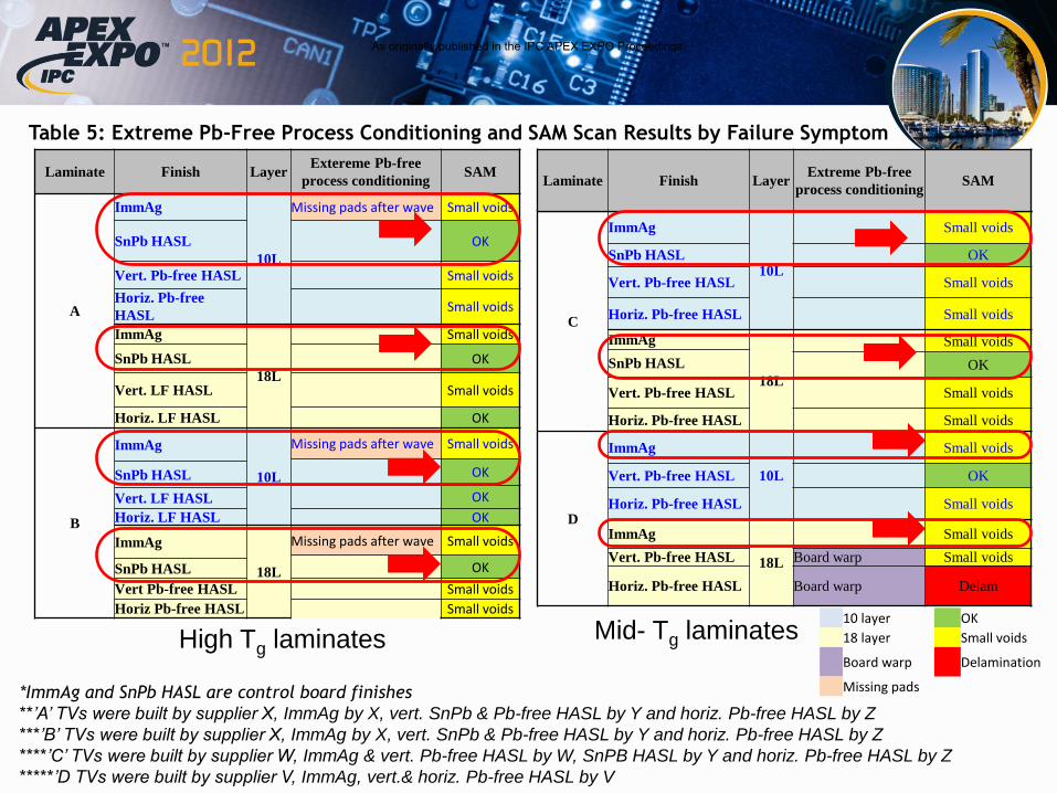
Table 5: Extreme Pb-free Process Conditioning and SAM Scan Results by Failure Symptom
Laminate Finish Layer Extreme Pb-Free process conditioning SAM
A
ImmAg
10L
Missing pads after wave soldering Small voids
SnPb HASL
OK
Vert. Pb-free HASL
Small voids
Horiz. Pb-free HASL
Small voids
ImmAg
18L
Small voids
SnPb HASL
OK
Vert. Pb-free HASL
Small voids
Horiz. Pb-free HASL
OK
B
ImmAg
10L
Missing pads after wave soldering Small voids
SnPb HASL
OK
Vert. Pb-free HASL
OK
Horiz. Pb-free HASL
OK
ImmAg
18L
Missing pads after wave soldering Small voids
SnPb HASL OK
Vert. Pb-free HASL Small voids
Horiz. Pb-free HASL
Small voids
C
ImmAg
10L
Small voids
SnPb HASL OK
Vert. Pb-free HASL Small voids
Horiz. Pb-free HASL Small voids
ImmAg
18L
Small voids
SnPb HASL OK
Vert. Pb-free HASL Small voids
Horiz. Pb-free HASL Small voids
D
ImmAg
10L
Small voids
Vert. Pb-free HASL OK
Horiz. Pb-free HASL Small voids
ImmAg
18L
Small voids
Vert. Pb-free HASL Board warp Small voids
Horiz. Pb-free HASL Board warp Delam
*ImmAg and SnPb HASL are control board finishes
**’A’ TVs were built by supplier X, ImmAg by X, vert. SnPb & Pb-free HASL by Y and horiz. Pb-free HASL by Z
***’B’ TVs were built by supplier X, ImmAg by X, vert. SnPb & Pb-free HASL by Y and horiz. Pb-free HASL by Z
****’C’ TVs were built by supplier W, ImmAg & vert. Pb-free HASL by W, SnPB HASL by Y and horiz. Pb-free HASL by Z
*****’D TVs were built by supplier V, ImmAg, vert.& horiz. Pb-free HASL by V
10 layer boards OK
18 layer boards Small voids
Board warp Delamination
Missing pads
As originally published in the IPC APEX EXPO Proceedings.

Table 6: Samples photos of voids/delamination:
Laminate/Layer/ Surface Finish Photos Zoom-in photos
Laminate A (10 layers) Immersion Silver
Laminate A (10 layers) Horizontal Pb-free HASL
Laminate A (18 layers) Vertical Pb-free HASL
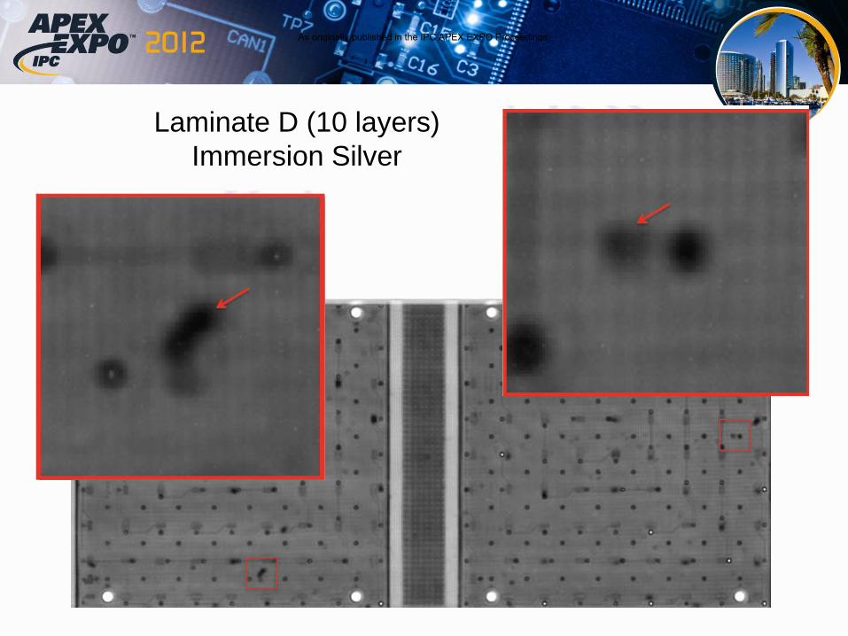
Laminate C (18 layers) Immersion Silver
Laminate D (18 layers) Horizontal Pb-free HASL
Discussion of Results
1. All control boards with SnPb HASL had no voiding. The immersion silver boards, which had 1 fewer thermal
cycle than any of the HASL boards, showed voiding. We do not understand this since logically the immersion silver
should have had less voiding than even SnPb HASL. It seems unlikely that random variation in the base material
would have produced this result, but no plausible explanation is known for the difference when writing this paper.
2. The immersion silver boards showed the same level of voiding as Pb-free HASL. This shows that the Pb-free
HASL itself was not the primary factor in voiding.
3. Vertical and horizontal HASL did not show any difference in voiding. Thermal impact between these 2 plating
processes on the boards is comparable.
4. Laminate D at 18L cannot survive the necessary process steps, showing delamination and warp. Board warp caused
solder overflow onto the board during wave soldering. This further confirms why dicy cured materials should not
be used for products which are undergoing Pb-free soldering and more so with Pb-free HASL surface finish.
5. Defect rate increases with higher layer count. As stack-up increases, the probability for any deficient bond between
the inner layer copper oxide and the “B” stage prepreg resin could potentially increase also. This may be caused by
lack of process control in any of the fabrication process, be it oxide process, control of heat-up rate during
lamination, prepreg with lower surface resin or control of etch back process.
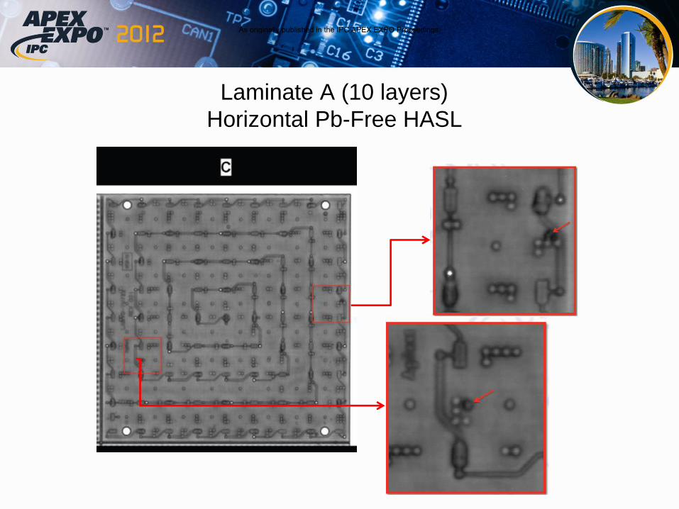
6. In this experiment, voids are assumed to be precursors to delamination. Boards with voids detected by SAM were
sent for cross-sections. The degradation of the material is often internal and not visible to external visual inspection,
necessitating SAM and cross-sections. Hence, the 99% yield for visual inspection on all boards. The 1% failure
was attributed by 2 warped boards and 1 delaminated board.
7. Some pads on the immersion silver plated PCBs were missing after wave. The extreme soak time of 7 seconds at
wave soldering reflects the worst case scenario of a Pb-free wave soldering profile. Immersion silver boards
immersed in the wave solder pot for this duration had pads missing.
As originally published in the IPC APEX EXPO Proceedings.
Conclusion
An important consideration for Pb-free materials, before any of the long-term reliability considerations are addressed, is the
survivability of the laminates without degradation after the Pb-free assembly process. This survivability is further stressed if
Pb-free HASL is used, which adds another thermal cycle to the board during the fabrication process. The HASL profile
shows that any laminate that is currently coated with tin lead HASL should be able to withstand the Pb-free HASL processing
temperatures under the same dip time conditions. The voiding of Pb-free HASL boards was the same as in the immersion
silver boards after extreme assembly conditions. As a chosen Pb-free compatible material approaches the 6 reflow and 1
wave thermal cycle limit, it is evident that we are very close to discovering more potential problems, with the early onset of
voids. This project concluded that material survivability performance of a Pb-free product depends on the type of material
that is used and layer count of the board.
Acknowledgements
The authors would like to thank the following individuals for their valuable inputs:
• Julie Silk and Bill Hanna of Agilent Technologies for technical support;
• Richard Coyle of Alcatel-Lucent for technical support;
• Chia Aik Shuen of Agilent Technologies for test vehicle design;
• DSUG extended team members of Agilent Technologies for their invaluable comments and feedback;
• Keith Sweatman, Makoto Hara, Pavithiran, WT Tan (Seribeau) of Nihon Superior and Mr. Fujimori of Vision
Technologies for vertical Pb-free HASL thermal profiling;
• Schweizer for horizontal Pb-free HASL plating;
• Multek, Fastprint, Dysteq for test vehicle fabrication;
• QAV for conducting SAM Thru scans;
• Celestica JB for processing the test vehicles through the extreme Pb-free manufacturing environment;
References
[1] "Considerations For Selecting A Printed Circuit Board Surface Finish", by R. Schueller, SMTA Int'l Proceedings, 2010.
[2] “The hidden art of manufacturing multi-layered PCBs” by Stephen Sher, Cirtech Electronics.
[3] “An Evaluation of Pb-free Surface Finishes’ by Khaw Mei Ming, Agilent Technologies, SMTA Penang Proceedings,
2010.
[4] "Hot air solder leveling in the Pb-free era"' by Keith Sweatman, Nihon Superior, featured in EM Asia, Sept-Oct 09.
As originally published in the IPC APEX EXPO Proceedings.

Evaluation of Laminates in
Pb-Free HASL Process and
Pb-Free Assembly
Environment
By Khaw Mei Ming, Andrey Lee
Agilent Technologies
Bayan Lepas, Malaysia
As originally published in the IPC APEX EXPO Proceedings.
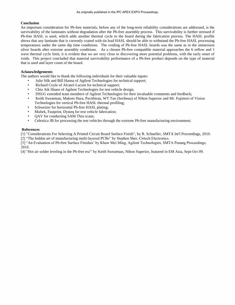
This paper focuses on 2 main evaluations.
DOE1: Compares the vertical SnPb and Pb-free HASL thermal profile at a
PCB fabricator for 2 different laminate materials.
DOE2: Studies the survivability of 4 different laminates (A, B, C, D)
through Pb-free HASL plating process followed by extreme Pb-free
manufacturing conditions.
Extreme Pb-free processing conditions: 2x reflow @260°C peak
(10secs), followed by 1x wave @270°C peak (7 sec) and 4x reflow
@260°C peak (10 sec).
Control surface finishes for comparison are SnPb HASL and
immersion silver.
Project Overview
As originally published in the IPC APEX EXPO Proceedings.

DOE1: Vertical Pb-Free HASL Thermal Profile
Objective
To compare 2 PCB material’s internal and surface temperatures during the HASL
dipping process in SnPb and SnCuNi solder alloy.
Test vehicle size: 11” x 11”
Number of layer count: 10
Overall board thickness: 1.9mm
Board material (A1, A2, B): High Tg laminate
Laminate A1
in SnCuNi
Laminate A2
in SnPb
Laminate B
in SnCuNi
Resin Type Unfilled Phenolic Filled Phenolic
Solder Temp., °C 265 260 265
Dipping Time, sec 7 7 5
Table1: DOE1 Test Condition
Note: No air knife was used during the evaluation
As originally published in the IPC APEX EXPO Proceedings.

Fig.1: Thermocouple Locations
Fig.2: Thermocouples
mounted on a profile board
Note
1. Thermocouples 1, 3 and 5 (blue squares) were secured on the PCB surface
using high melting point (HMP) wire and high temperature epoxy.
2. Thermocouples 2, 4 and 6 (red circles) were embedded into the center of the
internal PCB stack-up and secured using high temperature epoxy.
As originally published in the IPC APEX EXPO Proceedings.

Table 2: Thermal Profile and Data Compilation
* Control board under known conditions
**Typical SnPb HASL solder pot peak temp.(°C)/dipping time (s): 240-270°C/1-4 sec
***Typical Pb-Free HASL solder pot peak temp.(°C)/dipping time (s): 260-275°C/1-5sec
Laminate type Laminate A1 Laminate A2 Laminate B
Overall Profile
Solder alloy SnPb SnCuNi SnCuNi
Tg, °C 175 DSC 175 DSC 180 DSC
Solder Pot Temp, °C 260 265 265
Dipping Time, sec 7 7 5
Surface
Peak
Temp, °C
T1 (FILO) 226 227 227
T3 211 180 223
T5 (LIFO) 188 172 217
Internal
Peak
Temp, °C
T2 (FILO) 188 202 193
T4 172 169 179
T6 (LIFO) 169 128 172
T1
T3
T5
T2
T4
T6
T1 T3
T5
T2 T4
T6
T1
T3
T5
T2 T4
T6
As originally published in the IPC APEX EXPO Proceedings.

Discussion of Results
1. Comparing the same type of laminate, A1 and A2 were dipped into SnCuNi and
SnPb respectively for the same dipping time.
The surface temperatures peaked at 226⁰C for SnPb and 227⁰C for SnCuNi.
The internal peak temperatures are 188⁰C for SnPb and 202⁰C for SnCuNi.
Referring to the properties of SnCuNi, this alloy has a lower spread factor,
longer wettability and higher surface tension, plus a hotter solder pot is used. In
this study where the same length of dipping time is used, the SnCuNi is hotter
than the SnPb for the FILO board, and lower for the LIFO.
2. Comparing different laminates A2 and B, dipped into SnCuNi for 7 and 5 sec
respectively.
Both A2 and B board surfaces peaked at 227⁰C, with B having more uniform
temperature along the panel length.
For internal, A2 peaked at 202⁰C, B peaked at 193⁰C with more consistent
temperatures between the FILO and LIFO boards.
B, a filled laminate, had temperatures that were more consistent along the panel
length, implying faster heat absorption.
As originally published in the IPC APEX EXPO Proceedings.
DOE2: Pb-Free Assembly Process Survivability
PCB
Material
Resin
type
Layer
Count ImmAg
SnPb
HASL
Vertical
SnCuNi
HASL
Horizontal
SnCuNi
HASL
Extreme Pb-
Free process SAM
Cross-
section
A
Unfilled
Phenolic
10L 40 12 12 12 76 26 13
18L 12 8 8 8 36 24 12
B
Filled
Phenolic
10L 40 12 12 12 76 26 13
18L 12 8 8 8 36 10 5
C
Filled
Phenolic
10L 8 4 12 8 32 14 7
18L 8 4 12 8 32 20 10
D
Unfilled
Dicy
10L 8 0 12 12 32 12 6
18L 8 0 12 12 32 16 8
Table3: DOE2 Test Condition
This DOE evaluated the survivability of various combinations of surface finishes
with 4 different types of laminates through the Pb-free HASL process (for HASL
plated board) followed by 7 thermal cycles of Pb-free soldering. The test boards
were evaluated with SAM scans to check for inner layer defects.
As originally published in the IPC APEX EXPO Proceedings.

Test vehicles from PCB suppliers
Wave 1x@270C peak, 7 sec (*)
Reflow 2x@260C peak, 10sec (*)
Reflow 4x@260C peak, 10sec (*)
Thru scan SAM
(*) Open/short
measurements
are taken
before & after
every thermal
cycle.
Pb-Free Process at the Contract Manufacturer (CM)
As originally published in the IPC APEX EXPO Proceedings.
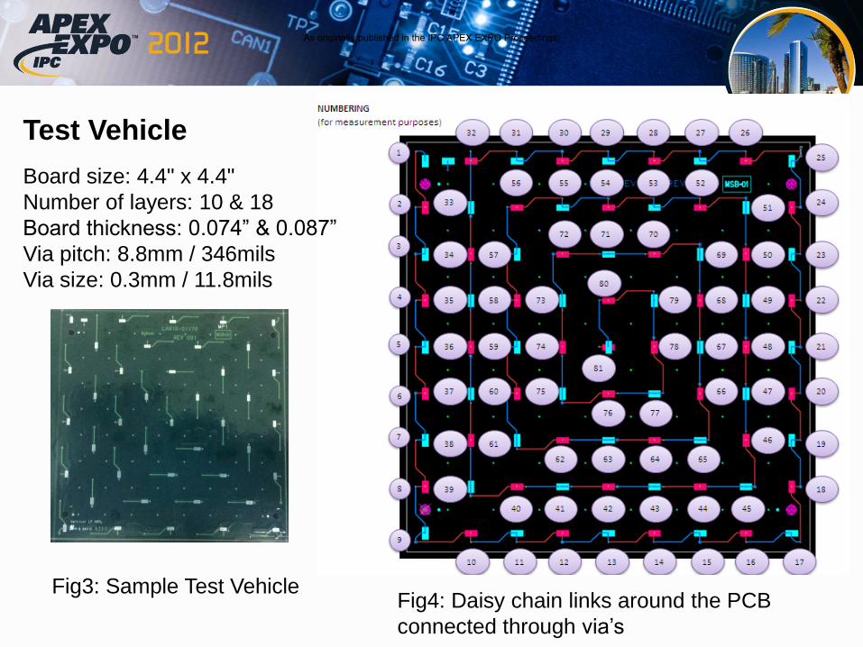
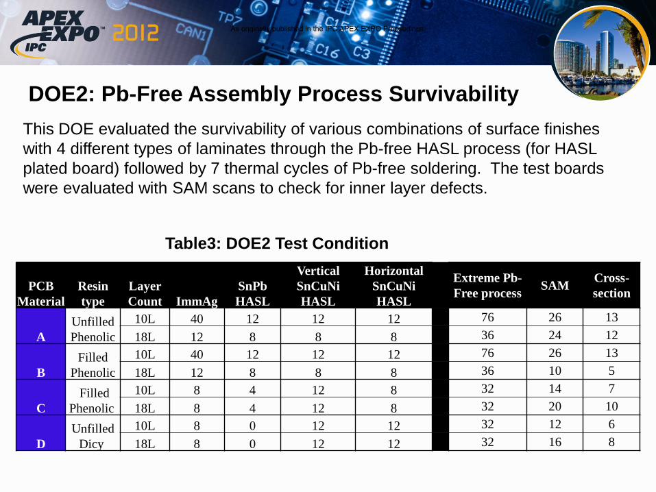
Fig4: Daisy chain links around the PCB
connected through via’s
Board size: 4.4" x 4.4"
Number of layers: 10 & 18
Board thickness: 0.074” & 0.087”
Via pitch: 8.8mm / 346mils
Via size: 0.3mm / 11.8mils
Test Vehicle
Fig3: Sample Test Vehicle
As originally published in the IPC APEX EXPO Proceedings.

Fig5: Reflow @260C peak @ 10sec Fig6: Wave @270C peak, 7sec
Fig7: Thru-scan in operation Fig8: Thru-scan imaging
As originally published in the IPC APEX EXPO Proceedings.

Laminate Finish Layer Visual
Insp.
Continuity
Test
# of
Scanned
brds
Scanned
Reject
Rate (%)
A
ImmAg
10L
36 33 8 38%
SnPb HASL 12 12 6 0%
12 12 6 17% Vert. Pb-Free
HASL
Horiz. Pb-
Free HASL 12 12 6 33%
ImmAg
18L
12 12 6 33%
SnPb HASL 8 8 6 0%
8 8 6 67% Vert. Pb-Free
HASL
Horiz. Pb-
Free HASL 8 8 6 0%
B
ImmAg
10L
36 34 8 25%
SnPb HASL 12 12 6 0%
12 12 6 0% Vert. Pb-Free
HASL
Horiz. Pb-
Free HASL 12 12 6 0%
ImmAg
18L
12 11 4 100%
SnPb HASL 8 8 2 0%
Vert. Pb-Free
HASL 8 8 2 100%
Horiz. Pb-
Free HASL 8 8 2 100%
Laminate Finish Layer Visual
Insp.
Continuity
Test
# of
Scanned
brds
Scanned
Reject Rate
(%)
C
ImmAg
10L
8 8 4 50%
SnPb HASL 4 4 2 0%
Vert. Pb-Free
HASL 12 12 6 33%
Horiz. Pb-
Free HASL 8 8 2 100%
ImmAg
18L
8 8 4 50%
SnPb HASL 4 4 4 0%
Vert. Pb-Free
HASL 12 12 6 33%
Horiz. Pb-
Free HASL 8 8 6 33%
D
ImmAg
10L
8 8 4 75%
Vert. Pb-Free
HASL 12 12 4 0%
Horiz. Pb-
Free HASL 12 12 4 50%
ImmAg
18L
8 8 6 33%
Vert. Pb-Free
HASL 11 12 6 33%
Horiz. Pb-
Free HASL 9 12 4 25%
*ImmAg and SnPb HASL are control board finishes
10 layer boards OK
18 layer boards Small voids
Board warp Delamination
Missing pads
Table 4: Extreme Pb-Free Process Conditioning and SAM Scan Results by Reject Rate
High-Tg laminates
Mid- Tg laminates
As originally published in the IPC APEX EXPO Proceedings.
C
ImmAg
10L
Small voids
SnPb HASL OK
Vert. Pb-free HASL Small voids
Horiz. Pb-free HASL Small voids
ImmAg
18L
Small voids
SnPb HASL OK
Vert. Pb-free HASL Small voids
Horiz. Pb-free HASL Small voids
D
ImmAg
10L
Small voids
Vert. Pb-free HASL OK
Horiz. Pb-free HASL Small voids
ImmAg
18L
Small voids
Vert. Pb-free HASL Board warp Small voids
Horiz. Pb-free HASL Board warp Delam
Laminate Finish Layer Extereme Pb-free
process conditioning SAM
A
ImmAg
10L
Missing pads after wave Small voids
SnPb HASL OK
Vert. Pb-free HASL Small voids
Horiz. Pb-free
HASL Small voids
ImmAg
18L
Small voids
SnPb HASL OK
Vert. LF HASL Small voids
Horiz. LF HASL OK
B
ImmAg
10L
Missing pads after wave Small voids
OK SnPb HASL
OK Vert. LF HASL
Horiz. LF HASL OK
ImmAg
18L
Missing pads after wave Small voids
OK SnPb HASL
Vert Pb-free HASL Small voids
Horiz Pb-free HASL Small voids
Laminate Finish Layer Extreme Pb-free
process conditioning SAM
Table 5: Extreme Pb-Free Process Conditioning and SAM Scan Results by Failure Symptom
High Tg laminates Mid- Tg laminates
*ImmAg and SnPb HASL are control board finishes
**’A’ TVs were built by supplier X, ImmAg by X, vert. SnPb & Pb-free HASL by Y and horiz. Pb-free HASL by Z
***’B’ TVs were built by supplier X, ImmAg by X, vert. SnPb & Pb-free HASL by Y and horiz. Pb-free HASL by Z
****’C’ TVs were built by supplier W, ImmAg & vert. Pb-free HASL by W, SnPB HASL by Y and horiz. Pb-free HASL by Z
*****’D TVs were built by supplier V, ImmAg, vert.& horiz. Pb-free HASL by V
10 layer OK
18 layer Small voids
Board warp Delamination
Missing pads
As originally published in the IPC APEX EXPO Proceedings.

Laminate A (10 layers)
Immersion Silver
As originally published in the IPC APEX EXPO Proceedings.

Laminate A (10 layers)
Horizontal Pb-free HASL
As originally published in the IPC APEX EXPO Proceedings.
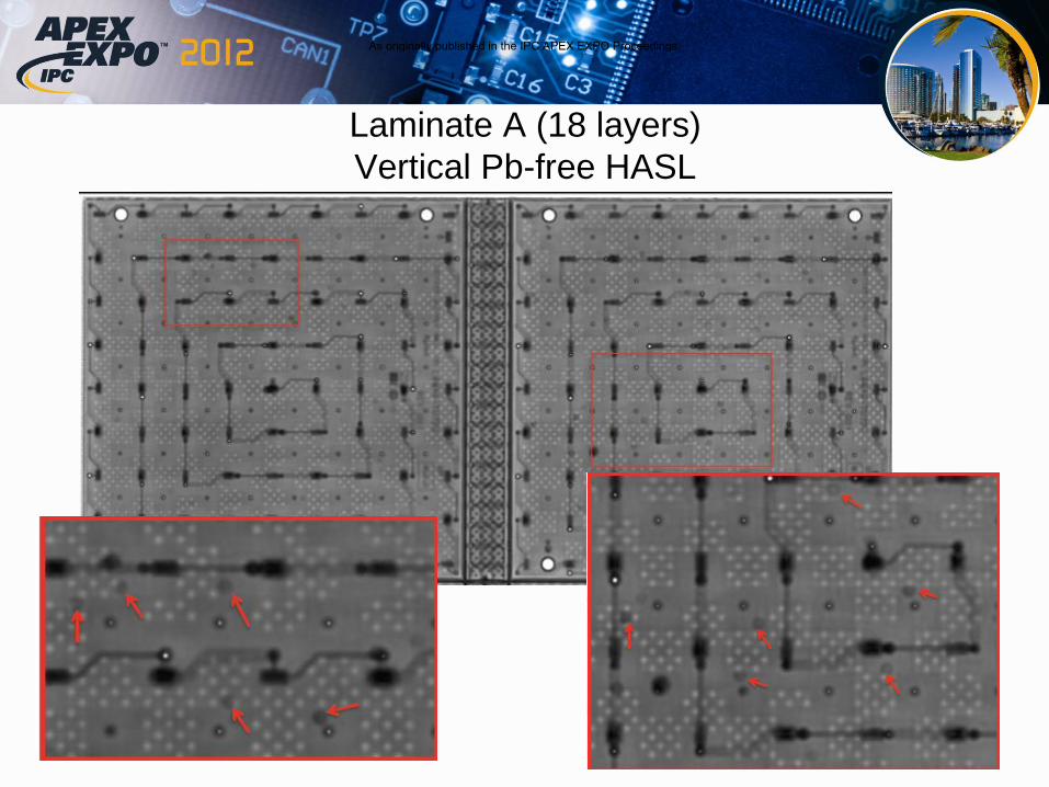
Laminate A (18 layers)
Vertical Pb-free HASL
As originally published in the IPC APEX EXPO Proceedings.

Laminate C (18 layers)
Immersion Silver
As originally published in the IPC APEX EXPO Proceedings.
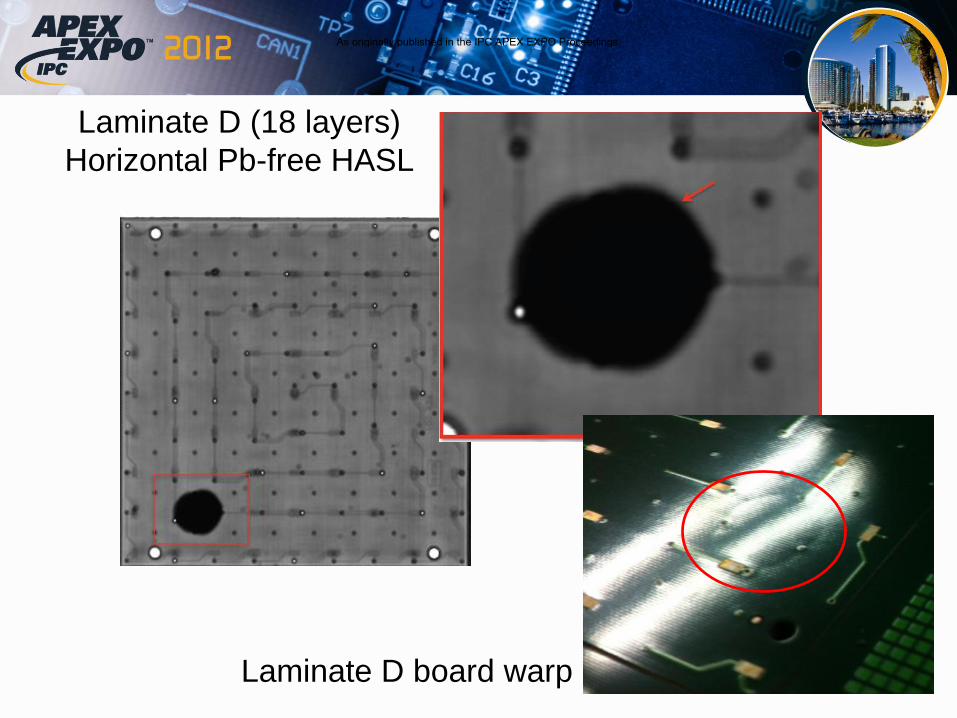
Laminate D (18 layers)
Horizontal Pb-free HASL
Laminate D board warp
As originally published in the IPC APEX EXPO Proceedings.
1. All control boards with SnPb HASL had no voiding.
• Immersion silver boards showed voiding. No plausible explanation.
2. The immersion silver boards showed the same level of voiding as Pb-free
HASL. This shows that the Pb-free HASL itself was not the primary factor in
voiding.
3. Vertical and horizontal HASL did not show any difference in voiding.
Thermal impact between these 2 plating processes on the boards is
comparable.
4. Laminate D at 18L cannot survive the necessary process steps, showing
delamination and warp.
• This further confirms why dicy cured materials should not be used for
products which are undergoing Pb-free soldering and more so with
Pb-free HASL surface finish.
Discussion of results:
As originally published in the IPC APEX EXPO Proceedings.

5. Defect rate increases with higher layer count.
• Cross-sections to determine failure location is not yet complete.
6. Voids are assumed to be precursors to delamination.
• Degradation of the material is often internal and not visible to external
visual inspection, necessitating SAM and cross-sections.
7. Pads on the immersion silver plated PCBs were missing after wave.
• The extreme soak time of 7 seconds at wave soldering reflects the worst
case scenario of a Pb-free wave soldering profile. Immersion silver
boards immersed in the wave solder pot for this duration had pads
missing.
Discussion (cont.):
As originally published in the IPC APEX EXPO Proceedings.
An important consideration for Pb-free materials, before any of the long-term
reliability considerations are addressed, is the survivability of the laminates
without degradation after the Pb-free assembly process. This survivability is
further stressed if Pb-free HASL is used which adds another thermal cycle to
the board during the fabrication process. As a chosen Pb-free compatible
material approaches the 6 reflow and 1 wave thermal cycle limit, it is evident
that we are very close to discovering more potential problems, with the early
onset of voids.
This project concluded that • Based on the HASL profiles, any laminate that is currently coated with tin
lead HASL should be able to withstand the Pb-free HASL processing
temperatures under the same dip time conditions.
• Material survivability performance of a Pb-free product depends on the type
of material that is used and layer count of the board.
• There is no difference between immersion silver, vertical or horizontal Pb-free
HASL on the reliability of the material.
Conclusions:
As originally published in the IPC APEX EXPO Proceedings.

Next Steps: Cross-sections…
to characterize the voids
to understand the root cause of the voids
As originally published in the IPC APEX EXPO Proceedings.
Acknowledgements
The authors would like to thank the following individuals for their valuable inputs:
• Julie Silk and Bill Hanna of Agilent Technologies for technical support;
• Richard Coyle of Alcatel-Lucent for technical support;
• Chia Aik Shuen of Agilent Technologies for test vehicle design;
• DSUG extended team members of Agilent Technologies for their invaluable
comments and feedback;
• Keith Sweatman, Makoto Hara, Pavithiran, WT Tan (Seribeau) of Nihon Superior
and Mr. Fujimori of Vision Technologies for vertical Pb-free HASL thermal profiling;
• Schweizer for horizontal Pb-free HASL plating;
• Multek, Fastprint, Dysteq for test vehicle fabrication;
• QAV for conducting SAM Thru scans;
• Celestica JB for processing the test vehicles through the extreme Pb-free
manufacturing environment;
As originally published in the IPC APEX EXPO Proceedings.
[1] "Considerations For Selecting A Printed Circuit Board Surface Finish",
by R. Schueller, SMTA Int'l Proceedings, 2010.
[2] “The hidden art of manufacturing multi-layered PCBs” by Stephen Sher,
Cirtech Electronics.
[3] “An Evaluation of Pb-free Surface Finishes’ by Khaw Mei Ming, Agilent
Technologies, SMTA Penang Proceedings, 2010.
[4] "Hot air solder leveling in the Pb-free era"' by Keith Sweatman, Nihon
Superior, featured in EM Asia, Sept-Oct 09.
References
As originally published in the IPC APEX EXPO Proceedings.
Thank you for your attention!
Any questions?
As originally published in the IPC APEX EXPO Proceedings.

Back-up slides
More examples of voids
As originally published in the IPC APEX EXPO Proceedings.
Laminate A (10 layers)
Horizontal Pb-Free HASL
As originally published in the IPC APEX EXPO Proceedings.

Laminate A (18 layers)
Immersion Silver
As originally published in the IPC APEX EXPO Proceedings.

Laminate B (18 layers)
Immersion Silver
As originally published in the IPC APEX EXPO Proceedings.

Laminate B (18 layers)
Vertical Pb-Free HASL
As originally published in the IPC APEX EXPO Proceedings.
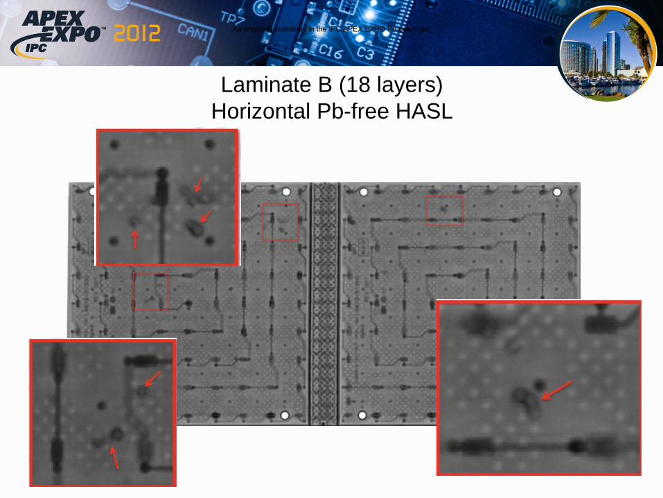
Laminate B (18 layers)
Horizontal Pb-free HASL
As originally published in the IPC APEX EXPO Proceedings.

Laminate C (10 layers)
Horizontal Pb-free HASL
As originally published in the IPC APEX EXPO Proceedings.
Laminate D (10 layers)
Immersion Silver
As originally published in the IPC APEX EXPO Proceedings.
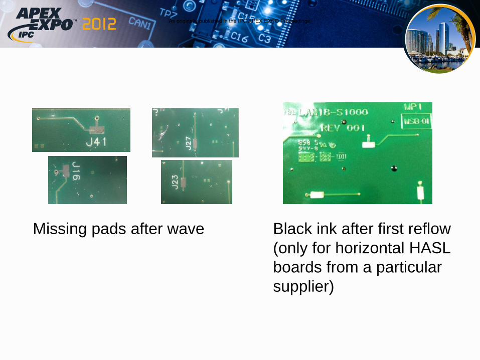
Missing pads after wave Black ink after first reflow
(only for horizontal HASL
boards from a particular
supplier)
As originally published in the IPC APEX EXPO Proceedings.