evolution of low drop out voltage regulator in cmos ...pe.org.pl/articles/2015/12/6.pdf · region...
TRANSCRIPT

26 PRZEGLĄD ELEKTROTECHNICZNY, ISSN 0033-2097, R. 91 NR 12/2015
Norhaida Binti Mustafa, Md. Syedul Amin, Mamun Bin Ibne Reaz, Fazida Hanim Hashim, Noorfazila Kamal
Universiti Kebangsaan Malaysia
doi:10.15199/48.2015.12.06
Evolution of Low Drop Out Voltage Regulator in CMOS Technologies
Abstract. The demand for low voltage devices has initiated the development of Low Drop Out (LDO) regulator in manifold. This paper presents a review of various LDO frameworks that have been implemented in CMOS technologies and the impact of frameworks related to the parameters of the LDO. The LDO architecture is evaluated through its Power Supply Rejection (PSR) and transient response performance. The transient response performance mostly depends on the added buffer and the PSR performance depends on the pass device capacitance and the LDO loop gain. \ Streszczenie. W artykule przedstawiono przegląd rozwiązań układów LDO (Low Drop Pout) w technologii CMOS. Przedstawiono także rozwiązania typu PSR – Power Supply Rejection. Analizowano dynamikę tych układów. Tendencje rozwojowe układów LDO (Low Drop Out) w technologii CMOS Keywords: CMOS, Low Drop Out (LDO) Regulator, Power Supply Rejection (PSR), transient response. Słowa kluczowe: układy LDO – Low Drop Out, technologia CMOS. Introduction
Power supply is one of the most vital modules in any electronic devices such as smart phones, tablet PCs, camera, MP3 player, Personal Data Assistant (PDA), Radio Frequency Identification (RFID) etc. [1-3]. Due to the rapid increasing demand for portable devices the use of efficient power management systems to prolong battery life cycle and operating time for device is becoming the most important factor [4-9]. A linear regulator is a popular power supply which is an inductor-less, ripple-less and low-noise power converter with a bulk line frequency transformer [10]. In the 1970s, the linear regulators have been implemented in BJT technology and are referred as the “20 kHz revolution” [7, 10]. However, the power efficiency was not sufficient for low-power operations as the ground current was load-current dependent and the dropout voltage was large [11]. In the 1980s, the power MOSFET appeared as the dominant power device due to its high-switching frequency operation (above 100 kHz), easier driving requirement and higher reliability [10]. With the rapid development of CMOS technology, many variations of CMOS voltage regulators have appeared [12-13]. There are several types of voltage regulators such as LDO linear regulator, Switch-Inductor Regulator (switching regulator) and Switch-Capacitor Regulator (charge pump) [4].
CMOS linear regulators can be categorized as low supply current, large current, high voltage, high-speed and Low Drop Out (LDO). The device that uses a low drop-out voltage regulator can provide a stable output voltage with good noise performance and less power consumption compared to switching regulators to drive small sub-circuit [5-6]. LDOs can operate at a low supply voltage, which is suitable for single-cell and two-cell battery applications as the ground current LDO is load-current independent [11]. In practical applications, such as portable devices, the conventional power management system consists of Switching Power Converter (SWPC) to boost up the voltage cascaded with LDOs in series to suppress the inherent noise associated with switchers and control logic [5, 14-15]. By turning the regulator’s outputs on and off or by varying the output voltage levels to optimize the power consumption of the device, the control logic can change the elements of each subsystem as active mode, standby mode and sleep mode [5].
This paper discusses the evolution of LDO voltage regulator based on CMOS technology and the various properties of existing regulator topologies with their
advantages. First the architecture, principle and specification of LDO are discussed and then the description of circuit, transient response and power supply rejection characteristics of the LDO voltage regulator are portrayed. Finally the discussion of all the framework are presented. Architecture and principle of LDO
The drop out voltage is the bare minimum differential voltage between the output and input voltage at such a point where the circuit stops to regulate. Also, low-dropout voltage indicates that the voltage across pass device is as low as 100mV to 1.5V [4]. For LDO regulator, the output voltage is always lower than input voltage by a minimum value of dropout voltage. The performance is enhanced as it has low output impedance. The LDO can be applied to high power, low power and ultra-low power applications.
LDO Linear Regulator Architecture
Basic LDO regulator topology usually consists of a pass device of PMOS, a decoupled capacitor CL with a parasitic resistor Resr, two feedback resistors R1 and R2, reference voltage and a critical error amplifier as shown in Figure 1. There are mainly three poles. p1 is from the output node, p2 is from the gate of the pass device and p3 is the internal pole within the error amplifier [16]. The basic schematic of generic LDO voltage regulators is based on a PMOS. The PMOS FET with common source connection works as the pass transistor between the input and output voltages. A part of the output voltage is fed back through R1 and R2 to the input and is compared to the voltage reference VREF. Capacitor CL stands for the capacitive load [17].
Fig. 1. Basic Low Dropout Regulator Topology [5]
The operating principle of LDO is based on the output of the regulator. It generates an error signal through the

PRZEGLĄD ELEKTROTECHNICZNY, ISSN 0033-2097, R. 91 NR 12/2015 27
feedback network to control the output current flow through the pass transistor. The output voltage is set to a constant voltage level by R1, R2 and reference voltage [5]. The divided voltage feedback through R1 and R2 and reference voltage difference, force the error amplifier to adjust the current flow through PMOS when changes happen at output voltage. The error amplifier compares the error signal with the reference voltage and amplifies the difference to control the pass device. A constant output voltage can be achieved by controlling the load current flow through the pass device. Output voltage is determined by Equation 1 [5]. The effi-ciency of LDO regulator can be expressed by Equation (2) and drop-out voltage can be expressed by Equation (3) [5].
(1) 1
(2) (3) 1
Error amplifier creates an error signal whenever there is a variation between the reference voltage and feedback voltage. The error signal controls the gate of power transistor for maintaining constant voltage with a supply of variable current to the load circuit as shown in Figure 2. This topology has the advantages of improved power supply rejection ratio (PSRR) and presents a dominant pole that is determined only by the load capacitance. The power consumption of the error amplifier is kept at minimum to avoid degrading the efficiency of the low voltage regulator (LVR). It uses a centroid configuration to minimize any offset voltage [18].
Fig. 2 . Error amplifier circuit [18]
To boost the output current capabilities of the error amplifier required by the load to the higher levels for maintaining the constant output value, the pass element is used. It requires to transfer large currents under the low power regulation of the error amplifier from the source voltage to the load [4]. Bipolar or MOS transistors can be used to implement the pass element. Smaller power consumption and consequently higher efficiency are offered by the MOS transistor. The main advantage of using the MOSFETs as the pass transistor is that, in addition to some gain, it also is self protected to short circuit current. As such, the additional short circuit protection circuit is not needed to some point [19]. The MOS transistor can be either N or P type. The NMOS as the power transistor had a large dropout voltage. Therefore, the NMOS transistor requires a gate voltage higher than the source voltage. Thus, a charge pump is necessary to increase the voltage
level [16]. The proper choice for low voltage systems is PMOS LDO [18] for obtaining a low dropout voltage which also results stability problem [16]. The pass device influ-ences loop gain, bandwidth, stability and dropout voltage.
Feedback network is a sampling resistor scales down the output voltage to a suitable value for comparing with the reference voltage by the error amplifier. To obtain the low power and voltage operation with small chip area, most of the transistors are designed to work at the sub threshold region and no resistor or bipolar transistor is required in voltage regulator. Feedback network in general is a voltage divider used to return part of the regulated voltage to the error amplifier input. If the desired regulated voltage is twice of the reference, the feedback network consists of two devices with same resistance in series with one end to output and one end to ground and the middle point connect to error amplifier.
VREF is used as a predefined reference level. A feedback signal of loading is compared with VREF by the error amplifier [20]. Off-chip external capacitors for to improving the transient-response and stability are at times required by the LDO regulators [4]. A voltage reference circuit is shown in Figure 3 [18].
Fig. 3. Voltage reference circuit [18]
LDO linear regulator specification Regulating performances, operating voltages and
quiescent current are the vital characteristics to be considered during designing LDO. Output capacitor and equivalent series resistance (ESR) range, load regulation, input/output voltage range, drop-out voltage, line regulation and output voltage variation are the other specifications [4].
Quiescent or ground current is the difference between output and input currents. To maximize the current efficiency, the low quiescent current is needed. The value of quiescent current is determined by the biasing currents of band gap, sampling resistor and error amplifier. The load regulation is defined as how much the output voltage varies with load current which depends on the LDO loop gain, Aβ, and the output impedance of the pass device, rop. The load regulation is approximately the ratio of the pass device output impedance to the loop gain. The smaller the output impedance of the pass device, the better is the load regulation. Since, the output impedance of the pass device cannot really be controlled, the loop gain should be designed to be high for best load regulation.
The line regulation of the LDO is defined as the output voltage variation due to input voltage variation. The output voltage should be independent of input voltage, so the ideal line regulation is zero. With a perfect input voltage reference, the dependent variables are loop gain, Aβ, and the gain of the pass device, gmprop. The line regulation is the ratio of the pass device gain to the loop gain.

28 PRZEGLĄD ELEKTROTECHNICZNY, ISSN 0033-2097, R. 91 NR 12/2015
The dropout voltage of the LDO is defined as the minimum voltage drop across the pass device to maintain regulation. The dropout voltage is typically specified at maximum load current. The maximum load current specifications determine the size of the pass device, dropout voltage and power dissipation constraints. When the maximum load current specification increases, the overall die area of the pass device, the control circuitry and the ground pin current increases in order to drive the additional parasitic capacitances of the increased device sizing.
PSR and transient response performance scheme
The low dropout regulators suffer from Power Supply Rejection Ratio (PSRR) and transient response in their implementations [4-5]. The PSRR measures the LDO’s ability to suppress the power supply noise [7]. It is also defined as how the output voltage changes with high frequency noise on the input voltage or the ability of a linear regulator to resist the high frequency noise at the input. The PSR is dependent on the pass device’s parasitic capacitances and LDO loop gain.
There are two types of transients; load and line. Load transients occur when the output current rapidly changes levels, such as a 1mA to 200mA step in load current. Load transient response usually reflects the loop gain, bandwidth and stability of the regulator. Line transients occur when the input voltage rapidly changes levels, such as a 4V to 5V step. Line transient response usually reflects the PSR of the regulator. For both load and line transients, important specifications are overshoot, undershoot and response time and are usually shown as a plot with a particular output capacitor. Decoupling capacitors with different values will put at the input to filter out the high frequency noise.
MOS Resistor as Feedback Network
The LDO framework without any external discrete components at feedback network was proposed by as shown in Figure 4 [18]. To achieve low power consumption and small silicon area, a source follower stage (MNFOL) and the replacement of the resistive sampler (R1 and R2) were introduced. The sampler was replaced by a single MOS transistor along with a grounded MOS resistor (biasing from transistor MNAUX). The source follower stage (transistor MNFOL) was added in order to provide stability to the LDO system. This LDO regulator was designed for important conditions such as low power consumption and low silicon area due the lack of external discrete components.
Fig. 4. Simplified diagram of linear voltage regulator [18]
PSR enhancer Recent improvement proposed by Park et al. as shown
in Figure 5 was the PSR-compensated LDO architecture with single-ended two-stage error amplifier, PSR enhancer and frequency compensation circuit [8]. For error amplifier, a fully-differential PMOS input stage is used to achieve high power supply noise rejection. PSR enhancer consists of a scaled replica of the pass transistor, a current buffer, a current amplifier and a current mirror. To achieve the loop stability, the frequency compensation zero is required by the combination of differentiator and amplification stage [8]. The frequency compensation also used to improve the transient response of LDO.
Fig. 5. PSR compensated LDO architecture [8]
Ganta et el. designed an LDO with transient and PSR enhancer [21]. The current amplifier was implemented by reusing the differentiator in the undershoot canceller as shown in Figure. 6. The current amplifier together with variable Cvdd serves as the PSR enhancer block. Cvdd samples and differentiates the power supply noise. The current is then converted into voltage by R1 and the converted back into current to the action of M2. Therefore, the capacitive current is then amplified by the current gain factor given by gm2R1 where gm2 is the transconductance of transistor M2. Most of the circuits are reused for both functions: overshoot and power supply noise cancellation.
Fig. 6. LDO with transient and PSR enhancer [21]

PRZEGLĄD ELEKTROTECHNICZNY, ISSN 0033-2097, R. 91 NR 12/2015 29
Super gain amplifier(SGA) and feed forward(FF) noise cancellation
The architecture of the LDO regulator proposed by Yuk et al. is shown in Figure. 7 [22]. It consists of an error amplifier (Ae1 and Ae2), a summing amplifier As, a buffer amplifier B, a main power MOSFET MP, a frequency compensator and a feedback network. The feed-forward block was for improving the high-frequency PSR of the LDO regulator. The PSR of the conventional LDO regulator is largely determined by the loop gain at very low frequency. The loop gain also determines the PSR.
Fig. 7. Architecture of the LDO regulator [22]
High pass filter and replica feedback loop
A highpass filter added in the replica feedback loop is proposed by Coulot et al. [23]. Highpass filter was used to avoid the PSR variation at low frequencies. It feeds forward the supply ripple and filters the DC offset and low-frequency components of Vrep, corresponding to the difference between load and replica. Hence, the PSR is constant at low frequencies, independent of the corresponding between the load and the replica, and becomes dependent on the amplifier gain.
Fig. 8. LDO regulator with highpass filter [23]
Two stage cascaded OTA The framework for LDO consisting of three main blocks:
An error amplifier, a voltage reference and a pass transistor with external load capacitance with small value of internal resistance (ESR) for the frequency compensation is proposed by [19]. Error amplifier using two-stage cascaded OTA in CMOS technology having a single ended output was used in the proposed design. Pass transistor element is the pMOS transistor whose dimensions are set to withstand maximum output current of 450 mA. Thus, dimensions were W=8000 μm, and L=1 μm. Since, the
usage of pMOS is as pass transistor in open drain configuration, there is an issue in the output impedance being very high, causing a pole within the unity gain frequency, decreasing the phase margin. Therefore, an external load capacitance (CL) with small value of internal resistance RESthere were needed R so that it forms a zero, nullifying the effect of pole formed by high output impedance. CL=35nF was chosen in the design.
Fig. 9. LDO voltage linear regulator [19]
Voltage control current source(VCCS) A buffer is required to drive the gate capacitance of
PMOS while designing the LDO framework, to get a fast transient response. A significant pole is stimulated by the gate capacitance which degrades the stability. As such, to keep significant pole faraway away from the dominant pole, a buffer was required. The LDO regulator proposed by Lin and Liu consists of an error amplifier, a mirror stage (M1-M6), a power transistor (Mpw), feedback resistors and an output capacitor as shown in Figure 9 [6]. The mirror stage could keep the bias current of the mirror stage proportional to the output current. The current IM1 was equal to K1xIo. The quiescent current of the LDO can be written as I´q =K1x10+Iqbase where the I'q,base is a constant factor. As such, when Io is low, the power loss from Iq x VDD can be decreased. The equation also shows that 1q will be big when Io goes high. In a heavy load condition, the large quiescent current may degrade the efficiency of the LDO. However, Io x Vo becomes dominant as found from the equ-ation of η2, when Io goes high. As such, the power loss resulted from Iq xVDD does not reduces the efficiency much [6].
Fig. 10. LDO architecture with Mirror Stage and VCCS [6]

30 PRZEGLĄD ELEKTROTECHNICZNY, ISSN 0033-2097, R. 91 NR 12/2015
LDO with VCCS is proposed by Li et al. as shown in Figure 11. A zero depending on the equivalent capacitor C and the feedback resistor R2 of VCCS is created according to node current at node vx. A stable zero could be achieved with VCCS with C and R2 staying unchanged. LDO can operate active or sleep modes in the proposed design. A stable LDO was achieved with a small 1pF on-chip capacitor.
Fig. 11. LDO regulator with VCCS [16]
Three gain stages and current follower LDO linear regulator presented by Huang et al. is shown
Figure 12 [24]. The regulator consisted of three gain stages and a current follower (CF). Mc1–Mc5 and Ma1–Ma3 are the CF. CF was inserted between the Miller compensation capacitor, Cm and the output of the first stage. The lumped output parasitic capacitance of the first and second stage is Cp1 and Cg. The equivalent open-loop output resistance of the LDO linear regulator is 1/gout (=RL//Ropass//(RF1+RF2)). This LDO regulator employed with a single Miller capacitor to reduce the dips and peaks of the output voltage and the settling time.
Fig. 12. LDO regulator [24]
ARC technique The block diagram of the LDO with ARC technique
proposed by Lin et al. is shown in Figure 13 [25]. The LDO was composed of a transconductance amplifier, a power transistor, an ARC circuit, an output capacitor with ESR and resistors. ESR frequency compensation was used to introduce a pole-zero cancellation to ensure closed-loop
stability. It is a simple and popular method to compensate the phase margin of the system. However, in case of load variations, ESR degenerates the overshoot/undershoot voltage and limits the performance of the regulator. An ARC technique was used in order to overcome this issue.
Fig. 13. LDO with ARC technique [25]
D2 Coupling Technique LDO architecture proposed by Zheng et al. is shown in
Figure 14 [26]. The design was consisted of includes two feedback control loops; outer transient enhancement loop and inner error correction loop. The inner loop is active for all operation conditions and formed by the transistors. A direct dynamic (D2) coupling technique was used to improve the transient response. Voltage variation at Vout and Vref is directly coupled to the voltage coupling node Vcout and Vcref. This was to adjust Iout and Iref and to establish two direct sensing paths for DVS reference tracking and load transient. Vout can vary drastically during load or DVS transients as there is no output filter capacitor. An outer transient enhancement loop with an adaptive transmission control (ATC) scheme is employed to overcome this. To enhance the large signal transient, a high-slew-rate push-pull comparator with a flipped voltage follower (FVF) input stage was employed. Both the drop-out voltage and the quiescent current were maintained at low levels to achieve high power efficiencies and current.
Fig. 14. System architecture of LDO regulator [26]
Buffer compensator The error amplifier proposed by Al-shyouin et al. was
realized by a transistors M1 – M6 with single-stage folded-cascade structure [27]. The pole p2 at the output of the

PRZEGLĄD ELEKTROTECHNICZNY, ISSN 0033-2097, R. 91 NR 12/2015 31
buffer was pushed sufficiently high frequencies by using dynamically biased shunt feedback with different load currents. The pass device Mp recognizes a common-source gain stage and be the second gain stage in the LDO. As such, the LDO structure can be utilized as a two-stage amplifier driving a large capacitive load with two poles located the LDO output and at N1. The utilization of a F range off-chip output capacitor CL makes the capacitive load large. Current-buffer or cascode-Miller frequency compensation wa used in the LDO structure for stabilization. The pole-splitting compensation was aimed for splitting two poles p1 at N1 and p0 at the LDO output to attain constancy in the full range of the load current.
Fig. 15. LDO using current-buffer compensation scheme [27]
A framework with programmable output was proposed
by Wu and Huang as shown in Figure 16 [5]. The design included error amplifier, power transistor, output off-chip compensated circuit (Resr, CL), feedback network (R1, R2, R3, R4), logic circuit and reference voltage to control the programmable output voltage for low dropout regulator. For decreasing the power consumption and dropout voltage of LDO as low as possible, large ratio of the channel-width-to channel- length was created. This increased the gate capacitance of the power transistor. With the large gate capacitance, the loop stability of LDO degraded. To generate a pole at high frequency, a buffer with low output impedance was added in between the power transistor and the error amplifier. The loop speed was improved when the buffer split the poles like the regular Miller compensating scheme. Two NMOS switch transistors and two resistors were added to form an adjustable LDO circuit to design a LDO with programmable output. The NMOS transistors were acted as an open-circuit or a short-circuit according to the control logic of the NMOS switch transistors. Thus, the
programmable LDO was able regulate four various voltages which was 0V, 1.8V, 2.5V and 3.3V. The LDO’s transient response improves when the current compensation circuit is added in front of the buffer [5].
Fig.16. Framework of LDO [5]
Gong et al. proposed an LDO as shown Figure 17 [7]. The system consisted of PMOS pass transistor, an error amplifier, the stepping several stages Miller compensation capacitor C2, Transient Enhancement Unit (TEU), buffer and feedback resistors R1 and R2. The PSRR performance for this circuit improved significantly to 50dB at 1MHz and 51dB at 100 KHz. 1pF Miller compensation capacitor was only used.
Fig. 17. Structure of LDO with TEU [7]
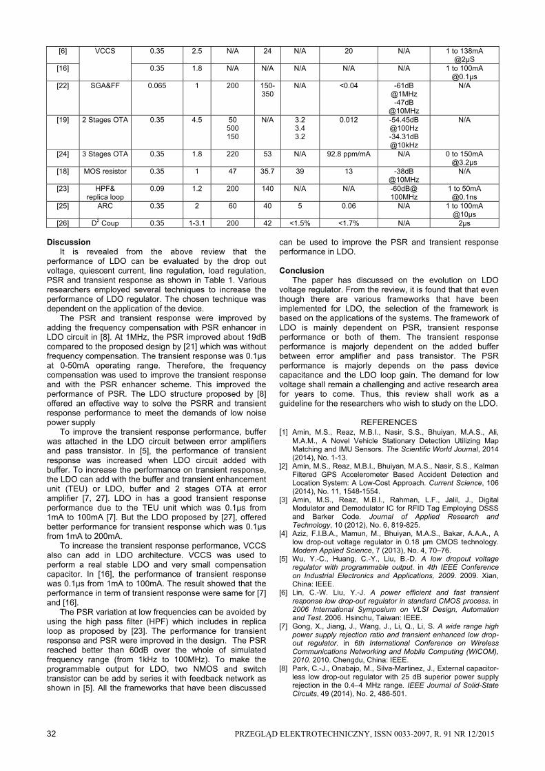
Table 3. Performance comparison PSRR and Transient scheme for LDO regulator
Ref LDO Scheme CMOS Tech. /µm
Parameter PSR (dB)
Transient Response
Vout (V)
Dropout (mV)
Iq (µA)
Line reg. mV/V
Load reg. mV/mA
[8] PSR Enhancer 0.18 1.6 200 55 75 0.14 -70dB @1MHz -37dB
@10MHz
0 to 50mA @0.1µs
[21] 0.18 N/A 200 0.018
N/A 0.03 -55dB @1MHz
0 to 50mA @1µS
[7] Buffer 0.35 N/A 767 0.063 2 0.5 -51.5dB @100KHz
-50dB @1MHz
1mA to 100mA @0.1µS
[27] 0.35 1.8 200 20 2 0.17 >45dB@ 0-20kHz
1 to 200mA @0.1µs
[5] 0.35 3.3 2.5 1.8
410 500 690
0.17 0.16 0.14
N/A N/A -63dB -68dB -71dB
@1kHz
0 to 100mA @2µS
32 PRZEGLĄD ELEKTROTECHNICZNY, ISSN 0033-2097, R. 91 NR 12/2015
[6] VCCS 0.35 2.5 N/A 24 N/A 20 N/A 1 to 138mA @2µS
[16] 0.35 1.8 N/A N/A N/A N/A N/A 1 to 100mA @0.1µs
[22] SGA&FF 0.065 1 200 150-350
N/A <0.04 -61dB @1MHz -47dB
@10MHz
N/A
[19] 2 Stages OTA 0.35 4.5 50 500 150
N/A 3.2 3.4 3.2
0.012 -54.45dB @100Hz -34.31dB @10kHz
N/A
[24] 3 Stages OTA 0.35 1.8 220 53 N/A 92.8 ppm/mA N/A 0 to 150mA @3.2µs
[18] MOS resistor 0.35 1 47 35.7 39 13 -38dB @10MHz
N/A
[23] HPF& replica loop
0.09 1.2 200 140 N/A N/A -60dB@ 100MHz
1 to 50mA @0.1ns
[25] ARC 0.35 2 60 40 5 0.06 N/A 1 to 100mA @10µs
[26] D2 Coup 0.35 1-3.1 200 42 <1.5% <1.7% N/A 2µs
Discussion It is revealed from the above review that the
performance of LDO can be evaluated by the drop out voltage, quiescent current, line regulation, load regulation, PSR and transient response as shown in Table 1. Various researchers employed several techniques to increase the performance of LDO regulator. The chosen technique was dependent on the application of the device.
The PSR and transient response were improved by adding the frequency compensation with PSR enhancer in LDO circuit in [8]. At 1MHz, the PSR improved about 19dB compared to the proposed design by [21] which was without frequency compensation. The transient response was 0.1µs at 0-50mA operating range. Therefore, the frequency compensation was used to improve the transient response and with the PSR enhancer scheme. This improved the performance of PSR. The LDO structure proposed by [8] offered an effective way to solve the PSRR and transient response performance to meet the demands of low noise power supply
To improve the transient response performance, buffer was attached in the LDO circuit between error amplifiers and pass transistor. In [5], the performance of transient response was increased when LDO circuit added with buffer. To increase the performance on transient response, the LDO can add with the buffer and transient enhancement unit (TEU) or LDO, buffer and 2 stages OTA at error amplifier [7, 27]. LDO in has a good transient response performance due to the TEU unit which was 0.1µs from 1mA to 100mA [7]. But the LDO proposed by [27], offered better performance for transient response which was 0.1µs from 1mA to 200mA.
To increase the transient response performance, VCCS also can add in LDO architecture. VCCS was used to perform a real stable LDO and very small compensation capacitor. In [16], the performance of transient response was 0.1µs from 1mA to 100mA. The result showed that the performance in term of transient response were same for [7] and [16].
The PSR variation at low frequencies can be avoided by using the high pass filter (HPF) which includes in replica loop as proposed by [23]. The performance for transient response and PSR were improved in the design. The PSR reached better than 60dB over the whole of simulated frequency range (from 1kHz to 100MHz). To make the programmable output for LDO, two NMOS and switch transistor can be add by series it with feedback network as shown in [5]. All the frameworks that have been discussed
can be used to improve the PSR and transient response performance in LDO.
Conclusion
The paper has discussed on the evolution on LDO voltage regulator. From the review, it is found that that even though there are various frameworks that have been implemented for LDO, the selection of the framework is based on the applications of the systems. The framework of LDO is mainly dependent on PSR, transient response performance or both of them. The transient response performance is majorly dependent on the added buffer between error amplifier and pass transistor. The PSR performance is majorly depends on the pass device capacitance and the LDO loop gain. The demand for low voltage shall remain a challenging and active research area for years to come. Thus, this review shall work as a guideline for the researchers who wish to study on the LDO.
REFERENCES
[1] Amin, M.S., Reaz, M.B.I., Nasir, S.S., Bhuiyan, M.A.S., Ali, M.A.M., A Novel Vehicle Stationary Detection Utilizing Map Matching and IMU Sensors. The Scientific World Journal, 2014 (2014), No. 1-13.
]2] Amin, M.S., Reaz, M.B.I., Bhuiyan, M.A.S., Nasir, S.S., Kalman Filtered GPS Accelerometer Based Accident Detection and Location System: A Low-Cost Approach. Current Science, 106 (2014), No. 11, 1548-1554.
[3] Amin, M.S., Reaz, M.B.I., Rahman, L.F., Jalil, J., Digital Modulator and Demodulator IC for RFID Tag Employing DSSS and Barker Code. Journal of Applied Research and Technology, 10 (2012), No. 6, 819-825.
[4] Aziz, F.I.B.A., Mamun, M., Bhuiyan, M.A.S., Bakar, A.A.A., A low drop-out voltage regulator in 0.18 µm CMOS technology. Modern Applied Science, 7 (2013), No. 4, 70–76.
[5] Wu, Y.-C., Huang, C.-Y., Liu, B.-D. A low dropout voltage regulator with programmable output. in 4th IEEE Conference on Industrial Electronics and Applications, 2009. 2009. Xian, China: IEEE.
[6] Lin, C.-W. Liu, Y.-J. A power efficient and fast transient response low drop-out regulator in standard CMOS process. in 2006 International Symposium on VLSI Design, Automation and Test. 2006. Hsinchu, Taiwan: IEEE.
[7] Gong, X., Jiang, J., Wang, J., Li, Q., Li, S. A wide range high power supply rejection ratio and transient enhanced low drop-out regulator. in 6th International Conference on Wireless Communications Networking and Mobile Computing (WiCOM), 2010. 2010. Chengdu, China: IEEE.
[8] Park, C.-J., Onabajo, M., Silva-Martinez, J., External capacitor-less low drop-out regulator with 25 dB superior power supply rejection in the 0.4–4 MHz range. IEEE Journal of Solid-State Circuits, 49 (2014), No. 2, 486-501.

PRZEGLĄD ELEKTROTECHNICZNY, ISSN 0033-2097, R. 91 NR 12/2015 33
[9] Amin, M., Mamun, M., Hashim, F., Husain, H., Separation of fetal electrocardiography (ECG) from composite ECG using adaptive linear neural network for fetal monitoring. International Journal of the Physical Sciences, 6 (2011), No. 24, 5871-5876.
[10] Liu, Y.-F. O'Mathuna, C., Editorial: Special Issue on Power Supply on Chip, 2013. IEEE Transactions on Power Electronics, 28 (2013), No. 9, 4125-4126.
[11] Leung, K.N. Mok, P.K., A CMOS voltage reference based on weighted ∆V GS for CMOS low-dropout linear regulators. IEEE Journal of Solid-State Circuits, 38 (2003), No. 1, 146-150.
[12] BintiMdSallah, S.S., Mohamed, H., Mamun, M., Amin, M.S., Cmos Downsizing: Present, Past And Future. Journal of Applied Sciences Research, 8 (2012), No. 8, 4138-4146.
[13]Aljarajreh, H., Reaz, M., Amin, M., Husain, H., An Active Inductor Based Low Noise Amplifier for RF Receiver. Electronics and Electrical Engineering, 19 (2013), No. 5, 49-52.
[14] Kankanamge, K., Kularatna, N., Steyn-Ross, D.A., Laplace transform-based theoretical foundations and experimental validation: low-frequency supercapacitor circulation for efficiency improvements in linear regulators. IET Power Electronics, 5 (2012), No. 9, 1785-1792.
[15] Al-Shyoukh, M. Lee, H., A compact ramp-based soft-start circuit for voltage regulators. IEEE Transactions on Circuits and Systems II: Express Briefs, 56 (2009), No. 7, 535-539.
[16] Li, Q., Qian, Y., Lv, D., Hong, Z. VCCS controlled LDO with small on-chip capacitor. in IEEE 10th International Conference on ASIC (ASICON), 2013 2013. Shenzhen, China: IEEE.
[17] Hicham, A. Qjidaa, H. A low drop-out voltage regulator in 90-nm CMOS technology. in 2012 International Conference on Complex Systems (ICCS). 2012. Agadir, Morocco.
[18] Crepaldi, P., Pimenta, T., Moreno, R. A CMOS low drop out voltage regulator. in 2010 International Conference on Microelectronics (ICM). 2010. Cairo, Egypt: IEEE.
[19] Martínez-García, H., Grau-Saldes, A., Bolea-Monte, Y. Design of a 4.5-V, 450-mA low-dropout voltage linear regulator based on a cascoded OTA. in 39th Annual Conference of the IEEE Industrial Electronics Society, IECON 2013. 2013. Vienna, Austria: IEEE.
[20] Hung, Y.C. Ceng, D.J. A Sub-1 V CMOS LDO Regulator with Multiple Protections Capabilities. in International Symposium on Computer, Consumer and Control (IS3C), 2014. 2014. Taichung, Taiwan: IEEE.
[21] Ganta, S., Park, C.-J., Gitzel, D., Rivera, R., Silva-Martinez, J. An external capacitor-less low drop-out regulator with superior PSR and fast transient response. in IEEE 56th International
Midwest Symposium on Circuits and Systems (MWSCAS), 2013. 2013. Columbus, OH: IEEE.
[22] Yuk, Y.-S., Jung, S., Kim, C., Gwon, H.-D., Choi, S., Cho, G.-H., PSR Enhancement Through Super Gain Boosting and Differential Feed-Forward Noise Cancellation in a 65-nm CMOS LDO Regulator. IEEE Transactions on Very Large Scale Integration (VLSI) Systems, 22 (2014), No. 10, 2181-2191.
[23] Coulot, T., Rouat, E., Fournier, J.-M., Lauga, E., Hasbani, F., High power supply rejection low-dropout regulator for ultra-low-power radiofrequency functions. Electronics Letters, 47 (2011), No. 20, 1117-1118.
[24] Huang, W.-J., Lu, S.-H., Liu, S.-I., CMOS low dropout linear regulator with single Miller capacitor. Electronics Letters, 42 (2006), No. 4, 216-217.
[25] Lin, C.-H., Chen, K.-H., Huang, H.-W., Low-dropout regulators with adaptive reference control and dynamic push–pull techniques for enhancing transient performance. IEEE Transactions on Power Electronics, 24 (2009), No. 4, 1016-1022.
[26] Zheng, C. Ma, D., Design of monolithic CMOS LDO regulator with coupling and adaptive transmission control for adaptive wireless powered bio-implants. IEEE Transactions on Circuits and Systems I: Regular Papers, 58 (2011), No. 10, 2377-2387.
[27] Al-Shyoukh, M., Lee, H., Perez, R., A transient-enhanced low-quiescent current low-dropout regulator with buffer impedance attenuation. IEEE Journal of Solid-State Circuits, 42 (2007), No. 8, 1732-1742.
Authors: Norhaida Binti Mustafa, Department of Electrical, Electronic and Systems Engineering,Universiti Kebangsaan Malaysia, 43600 UKM, Bangi, Selangor, Malaysia, E-mail: [email protected]; Md. Syedul Amin, Department of Electrical, Electronic and Systems Engineering,Universiti Kebangsaan Malaysia, 43600 UKM, Bangi, Selangor, Malaysia, E-mail: [email protected]; Mamun Bin Ibne Reaz, Department of Electrical, Electronic and Systems Engineering,Universiti Kebangsaan Malaysia, 43600 UKM, Bangi, Selangor, Malaysia, E-mail: [email protected]; Fazida Hanim Hashim, Department of Electrical, Electronic and Systems Engineering,Universiti Kebangsaan Malaysia, 43600 UKM, Bangi, Selangor, Malaysia, E-mail: [email protected]; Noorfazila Kamal, Department of Electrical, Electronic and Systems Engineering,Universiti Kebangsaan Malaysia, 43600 UKM, Bangi, Selangor, Malaysia, E-mail: [email protected].