exceptional points in fano-resonant graphene...
TRANSCRIPT
Exceptional points in Fano-resonant graphene metamaterials
QINGJIE LIU,1 BING WANG,1,* SHAOLIN KE,1 HUA LONG,1 KAI WANG,1 AND
PEIXIANG LU1,2,3
1Wuhan National Laboratory for Optoelectronics and School of Physics, Huazhong University of Science and Technology, Wuhan 430074, China 2Laboratory of Optical Information Technology, Wuhan Institute of Technology, Wuhan 430205, China [email protected] *[email protected]
Abstract: We investigate the optical exceptional points (EPs) in the graphene incorporated multilayer metamaterial manifesting Fano resonance. The system is non-Hermitian and possesses EPs where both the eigenvalues and eigenvectors of the Hamiltonian coalesce. In the aid of Fano resonance, the reflection may reach minimum approaching to zero, resulting in the degeneration of both eigenvalues and eigenvectors and thus the emergence of EPs. The transmission and reflection of light through the metamaterial change sharply by varying slightly the incident wavelength and chemical potential of graphene in the parameter space when encircling the EPs. In addition, the unidirectional invisibility can be achieved at EPs. The study paves a way to precisely controlling the transmission and reflection through metamaterials and may find applications in optoelectronic switches, modulators, absorbers, and optical sensors. © 2017 Optical Society of America
OCIS codes: (240.6680) Surface plasmons; (160.3918) Metamaterials.
References and links
1. M. Lawrence, N. Xu, X. Zhang, L. Cong, J. Han, W. Zhang, and S. Zhang, “Manifestation of PT symmetry breaking in polarization space with terahertz metasurfaces,” Phys. Rev. Lett. 113(9), 093901 (2014).
2. Z. Lin, H. Ramezani, T. Eichelkraut, T. Kottos, H. Cao, and D. N. Christodoulides, “Unidirectional invisibility induced by PT-symmetric periodic structures,” Phys. Rev. Lett. 106(21), 213901 (2011).
3. S. Feng, “Loss-induced super scattering and gain-induced absorption,” Opt. Express 24(2), 1291–1304 (2016). 4. L. Feng, Y. L. Xu, W. S. Fegadolli, M. H. Lu, J. E. B. Oliveira, V. R. Almeida, Y. F. Chen, and A. Scherer,
“Experimental demonstration of a unidirectional reflectionless parity-time metamaterial at optical frequencies,” Nat. Mater. 12(2), 108–113 (2012).
5. M. Kang, H. Cui, T. Li, J. Chen, W. Zhu, and M. Premaratne, “Unidirectional phase singularity in ultrathin metamaterials at exceptional points,” Phys. Rev. A 89(6), 065801 (2014).
6. L. Feng, X. Zhu, S. Yang, H. Zhu, P. Zhang, X. Yin, Y. Wang, and X. Zhang, “Demonstration of a large-scale optical exceptional point structure,” Opt. Express 22(2), 1760–1767 (2014).
7. C. Dembowski, H. Gräf, H. L. Harney, A. Heine, W. D. Heiss, H. Rehfeld, and A. Richter, “Experimental observation of the topological structure of exceptional points,” Phys. Rev. Lett. 86(5), 787–790 (2001).
8. S. Ke, B. Wang, C. Qin, H. Long, K. Wang, and P. Lu, “Exceptional points and asymmetric mode switching in plasmonic waveguides,” J. Lightwave Technol. 34(22), 5258–5262 (2016).
9. T. Gao, E. Estrecho, K. Y. Bliokh, T. C. Liew, M. D. Fraser, S. Brodbeck, M. Kamp, C. Schneider, S. Höfling, Y. Yamamoto, F. Nori, Y. S. Kivshar, A. G. Truscott, R. G. Dall, and E. A. Ostrovskaya, “Observation of non-Hermitian degeneracies in a chaotic exciton-polariton billiard,” Nature 526(7574), 554–558 (2015).
10. H. X. Cui, X. W. Cao, M. Kang, T. F. Li, M. Yang, T. J. Guo, Q. H. Guo, and J. Chen, “Exceptional points in extraordinary optical transmission through dual subwavelength metallic gratings,” Opt. Express 21(11), 13368–13379 (2013).
11. B. Dietz, H. L. Harney, O. N. Kirillov, M. Miski-Oglu, A. Richter, and F. Schäfer, “Exceptional points in a microwave billiard with time-reversal invariance violation,” Phys. Rev. Lett. 106(15), 150403 (2011).
12. R. Yu, V. Pruneri, and F. J. García de Abajo, “Resonant visible light modulation with graphene,” ACS Photonics 2(4), 550–558 (2015).
13. P. Y. Chen, M. Farhat, A. N. Askarpour, M. Tymchenko, and A. Alù, “Infrared beam-steering using acoustically modulated surface plasmons over a graphene monolayer,” J. Opt. 16(9), 094008 (2014).
Vol. 25, No. 7 | 3 Apr 2017 | OPTICS EXPRESS 7203
#285409 https://doi.org/10.1364/OE.25.007214 Journal © 2017 Received 24 Jan 2017; revised 16 Mar 2017; accepted 16 Mar 2017; published 20 Mar 2017
14. J. Christensen, A. Manjavacas, S. Thongrattanasiri, F. H. Koppens, and F. J. García de Abajo, “Graphene plasmon waveguiding and hybridization in individual and paired nanoribbons,” ACS Nano 6(1), 431–440 (2012).
15. H. Ramezani, Y. Wang, E. Yablonovitch, and X. Zhang, “Unidirectional perfect absorber,” IEEE J. Sel. Top. Quantum Electron. 22(5), 115–120 (2016).
16. H. Huang, S. Ke, B. Wang, H. Long, K. Wang, and P. Lu, “Numerical study on plasmonic absorption enhancement by a rippled graphene sheet,” J. Lightwave Technol. 35(2), 320–324 (2017).
17. F. Wang, C. Qin, B. Wang, H. Long, K. Wang, and P. Lu, “Rabi oscillations of Plasmonic Supermodes in Graphene Multilayer Arrays,” IEEE J. Sel. Top. Quantum Electron. 23(1), 125–129 (2017).
18. C. Qin, B. Wang, H. Long, K. Wang, and P. Lu, “Nonreciprocal phase shift and mode modulation in dynamic graphene waveguides,” J. Lightwave Technol. 34(16), 3877–3883 (2016).
19. Z. Wang, B. Wang, K. Wang, H. Long, and P. Lu, “Vector plasmonic lattice solitons in nonlinear graphene-pair arrays,” Opt. Lett. 41(15), 3619–3622 (2016).
20. X. Zhang, X. Zhu, X. Liu, D. Wang, Q. Zhang, P. Lan, and P. Lu, “Ellipticity-tunable attosecond XUV pulse generation with a rotating bichromatic circularly polarized laser field,” Opt. Lett. 42(6), 1027–1030 (2017).
21. M. Amin, M. Farhat, and H. Baǧcı, “A dynamically reconfigurable Fano metamaterial through graphene tuning for switching and sensing applications,” Sci. Rep. 3, 2105 (2013).
22. P. Q. Liu, I. J. Luxmoore, S. A. Mikhailov, N. A. Savostianova, F. Valmorra, J. Faist, and G. R. Nash, “Highly tunable hybrid metamaterials employing split-ring resonators strongly coupled to graphene surface plasmons,” Nat. Commun. 6(4), 8969 (2015).
23. A. E. Miroshnichenko, S. Flach, and Y. S. Kivshar, “Fano resonances in nanoscale structures,” Rev. Mod. Phys. 82(3), 2257–2298 (2010).
24. B. Luk’yanchuk, N. I. Zheludev, S. A. Maier, N. J. Halas, P. Nordlander, H. Giessen, and C. T. Chong, “The Fano resonance in plasmonic nanostructures and metamaterials,” Nat. Mater. 9(9), 707–715 (2010).
25. Y. Zhang, T. Li, B. Zeng, H. Zhang, H. Lv, X. Huang, W. Zhang, and A. K. Azad, “A graphene based tunable terahertz sensor with double Fano resonances,” Nanoscale 7(29), 12682–12688 (2015).
26. X. Han, K. Wang, H. Long, H. Hu, J. Chen, B. Wang, and P. Lu, “Highly sensitive detection of the lattice distortion in single bent ZnO nanowires by second-harmonic generation microscopy,” ACS Photonics 3(7), 1308–1314 (2016).
27. M. Pan, Z. Liang, Y. Wang, and Y. Chen, “Tunable angle-independent refractive index sensor based on Fano resonance in integrated metal and graphene nanoribbons,” Sci. Rep. 6(1), 29984 (2016).
28. E. D. Palik, “refractive index,” in Handbook of Optical Constants of Solids 5–114 (Academic 1997). 29. B. Wang, X. Zhang, F. J. García-Vidal, X. Yuan, and J. Teng, “Strong coupling of surface plasmon polaritons in
monolayer graphene sheet arrays,” Phys. Rev. Lett. 109(7), 073901 (2012). 30. V. P. Gusynin, S. G. Sharapov, and J. P. Carbotte, “Magneto-optical conductivity in graphene,” J. Phys.
Condens. Matter 19(2), 026222 (2007). 31. P. Lalanne and G. M. Morris, “Highly improved convergence of the coupled-wave method for TM polarization,”
J. Opt. Soc. Am. A 13(4), 779–784 (1996). 32. J. A. Porto, F. J. García-Vidal, and J. B. Pendry, “Transmission Resonances on Metallic Gratings with Very
Narrow Slits,” Phys. Rev. Lett. 83(14), 2845–2848 (1999). 33. K. S. Novoselov, A. K. Geim, S. V. Morozov, D. Jiang, Y. Zhang, S. V. Dubonos, I. V. Grigorieva, and A. A.
Firsov, “Electric field effect in atomically thin carbon films,” Science 306(5696), 666–669 (2004). 34. H. Yan, T. Low, W. Zhu, Y. Wu, M. Freitag, X. Li, F. Guinea, P. Avouris, and F. Xia, “Damping pathways of
mid-infrared plasmons in graphene nanostructures,” Nat. Photonics 7(5), 394–399 (2013). 35. A. Vakil and N. Engheta, “Transformation optics using graphene,” Science 332(6035), 1291–1294 (2011). 36. P. Y. Chen and A. Alù, “Atomically thin surface cloak using graphene monolayers,” ACS Nano 5(7), 5855–5863
(2011). 37. A. Woessner, M. B. Lundeberg, Y. Gao, A. Principi, P. Alonso-González, M. Carrega, K. Watanabe, T.
Taniguchi, G. Vignale, M. Polini, J. Hone, R. Hillenbrand, and F. H. L. Koppens, “Highly confined low-loss plasmons in graphene-boron nitride heterostructures,” Nat. Mater. 14(4), 421–425 (2014).
38. K. I. Bolotin, K. J. Sikes, Z. Jiang, M. Klima, G. Fudenberg, J. Hone, P. Kim, and H. L. Stormer, “Ultrahigh electron mobility in suspended graphene,” Solid State Commun. 146(9–10), 351–355 (2008).
39. I. Gierz, J. C. Petersen, M. Mitrano, C. Cacho, I. C. Turcu, E. Springate, A. Stöhr, A. Köhler, U. Starke, and A. Cavalleri, “Snapshots of non-equilibrium Dirac carrier distributions in graphene,” Nat. Mater. 12(12), 1119–1124 (2013).
40. J. C. Johannsen, S. Ulstrup, F. Cilento, A. Crepaldi, M. Zacchigna, C. Cacho, I. C. E. Turcu, E. Springate, F. Fromm, C. Raidel, T. Seyller, F. Parmigiani, M. Grioni, and P. Hofmann, “Direct view of hot carrier dynamics in graphene,” Phys. Rev. Lett. 111(2), 027403 (2013).
41. D. Brida, A. Tomadin, C. Manzoni, Y. J. Kim, A. Lombardo, S. Milana, R. R. Nair, K. S. Novoselov, A. C. Ferrari, G. Cerullo, and M. Polini, “Ultrafast collinear scattering and carrier multiplication in graphene,” Nat. Commun. 4(3), 1987–1995 (2013).
Vol. 25, No. 7 | 3 Apr 2017 | OPTICS EXPRESS 7204

1. Introduction
In an open quantum system with parity-time symmetry, the Hamiltonian is non-Hermitian but possesses purely real eigenvalues. Once the parity-time (PT) symmetry is broken, the eigenvalues are no longer real and become complex. Subsequently, the eigenvalues and eigenfunctions of the Hamiltonian coalesce and the exceptional points (EPs) may emerge. Therefore EPs are also known as PT symmetry breaking points. EPs have been theoretically proposed and experimentally demonstrated in PT systems composed of gain and loss media [1–4]. In fact, the formation of EPs requires only non-Hermiticity and the PT symmetry is not necessary [5]. Due to the degeneracy of eigenvalues and eigenvectors at EPs, the unidirectional zero reflection should happen. The unique characteristic can be applied in turn to find EPs [4, 6]. Another interesting feature of EPs lies in its topological property. The topological structure of EPs has been intensively investigated in microwave cavities [7], waveguides [8], and exciton-polariton billiards [9]. For example, Dembowski et al. have observed experimentally the topological structure of EPs in microwave cavities [7], where anti-crossing (crossing) of the real and imaginary parts of eigenvalues is presented and the eigenvalues and eigenvectors are interchanged from one state to another while encircling an EP.
So far EPs have been observed in a diversity of structures such as metallic films [3], metallic gratings [10], and microwave billiards [11]. Of which EPs are realized by tuning the real and imaginary parts of dielectric constant or structural parameters. The lossy metamaterials are non-Hermitian and can also be utilized to yield EPs [4]. Recently, graphene has been widely employed into metamaterials to realize many unique optoelectronic functionalities [12–14]. Graphene is lossy due to the limited relaxation time of electrons. As a result, the graphene incorporated metamaterials can constitute a non-Hermitian system. On the other hand, a convenient approach to realizing EPs is to find the zero reflection points, which can be implemented by using Fano resonance. Fano resonance is generated when a narrowband discrete state interferes with a broadband continuum. In view of photons, Fano resonance is caused when photons take different paths caused by the interference, leading to a photon trapping in continuum. The photon trapping annihilates the reflection on one side of the system [15], resulting in unidirectional zero reflection and the realization of EPs. Consequently, Fano resonance can be applied to graphene metamaterials to realize EPs by employing the highly tunable property of graphene. By adjusting the conductance of graphene, the peak position and values of the Fano-type reflection can be altered.
In this work, by employing the unique tunability of graphene [16–20] and the merits of Fano resonance [21–25], we exploit the EPs in graphene metamaterials under Fano resonance. The structure is a hybrid metamaterial employing double-layer metallic grating structure and single-layer graphene nanoribbons. Instead of changing the dielectric constant or structural parameters of the system, the chemical potential of graphene is tuned to adjust the valleys of Fano-type reflection. Furthermore, the topological structure of the EP is explored while encircling the EP in parameter space. The EPs associated with Fano resonance show unidirectional reflections and the resonance wavelength change with the optical parameters, which may find applications in optical sensors and environment detection [26].
2. Fano resonance and EPs in graphene metamaterials
The metamaterial structure considered to realize EPs is shown in Fig. 1. The structure consists of double layers of silver grating and a single layer of graphene ribbons. The heights of upper and bottom silver strips are h1 = 220 nm, h2 = 155 nm, respectively. The thickness of the spacer between them is h0 = 350 nm. The period of the Ag strips are uniformly set as d = 675 nm, and the width is wm1 = 600 nm, wm2 = 525 nm. The graphene ribbons have a width of wg = 75 nm, which are embedded at the bottom of upper grating grooves. The refractive index of the spacer between the two gratings is given by nd = 1.78 [27]. The refractive index of silver is obtained from experimental data [28]. The dielectric constant of graphene is εg(ω) = 1 +
Vol. 25, No. 7 | 3 Apr 2017 | OPTICS EXPRESS 7205

iσg(ω)/ε0ωΔ [29], where Δ = 1 nm is the equivalent thickness of graphene and ε0 is the permittivity in vacuum. The surface conductivity of graphene σg is governed by the Kubo formula [30–33], which includes the interband and intraband transition contributions, that is σg = σintra + σinter. As ħω < 2μc, the intraband transition dominates and the surface conductivity can simplify to a Drude-like formula as σg = ie2μc/πħ
2(ω + iτ−1) with e being the electron charge, μc the chemical potential, and τ the momentum relaxation time. Here the momentum relaxation time is decided by τ = μμc/eVF
2, while μ is the DC carrier mobility, VF is the Fermi velocity of electron. The temperature is 300 K and the Fermi velocity is 108 cm/s. The mobility is chosen as 10 000 cm2V−1s−1, which is in accordance with the experimental results [30]. It’s worth noting that the surface conductivity σg will be affected by its adjacent materials. When applying electric field to graphene, the influence of adjacent materials on the chemical potential and surface conductivity can be compensated. The electric field can be applied by utilizing the upper metal grating as the front-gate and the spacer as the back. The electric field should influence the carrier density and hence change the chemical potential.
Fig. 1. Schematic of the Ag-graphene hybrid structure. The graphene nanoribbons are deposited on the slits of the upper Ag strips. The structural parameters are: h1 = 220 nm, h0 = 350 nm, h2 = 155 nm, wg = 75 nm, wm1 = 600 nm, wm2 = 525 nm and d = 675 nm. Inset is the cross section of the design. The structure is excited by TM-polarized incident light with the magnetic field parallel to the grating.
For the structure shown in Fig. 1, the amplitudes of incident and scattered waves can be connected by the scattering matrix in the form
1 2 1 2
2 1 2 1
,b a t r a
Sb a r t a
= =
(1)
where a1 and a2 are amplitudes of incoming waves from positive and negative directions, and b1 and b2 are amplitudes of outgoing wave from negative and positive directions, respectively, as shown in the inset of Fig. 1. The equation is analogous to the time-independent Schrodinger equation with S having the equal status of the Hamiltonian. For simplicity, we do not consider the influence of the substrate beneath the metamaterial. Since then the system is reciprocal and the transmission coefficients on both sides are the same and represented by t. However, the reflection coefficients at different sides should be different and are denoted by r1 and r2, respectively. Note that the coefficients r1, r2, and t are all complex values since the loss of metal and graphene in the structure. If the system is lossless, the reflection and transmission coefficients are all real numbers, thus no EPs can be realized. The eigenvalues of Eq. (1) are s1,2 = t ± (r1r2)
1/2, and the corresponding eigenvectors are (r11/2, ± r2
1/2). Based on the fact that eigenvalues and eigenvectors coalesce at EPs, the EPs are therefore located at
Vol. 25, No. 7 | 3 Apr 2017 | OPTICS EXPRESS 7206
(r1r2)1/2 = 0. As a result, EPs appear when either r1 or r2 is zero. The reflection coefficients at
the two sides of the metamaterial can be written as r1,2 = |r1,2|exp(iφ1,2), where φ1 and φ2 are the reflection phases corresponding to reflection coefficients r1 and r2. Then we have the reflections R1,2 = |r1,2|
2. The condition for realizing EPs becomes making R1 or R2 be zero. As R1R2 = 0, the related reflection phase φ1 or φ2 has to experience a dislocation, which is a unique property of EPs. The zero reflection and phase dislocation can be unitized to seek out EPs in turn. Since it is difficult to make both R1 and R2 be zero simultaneously, the structure designed in Fig. 1 is asymmetric on the top and bottom. Additionally, such an asymmetric configuration supports two EPs that may expand the application of the structure. In experiment, the large-area graphene film could be first grown using an optimized liquid precursor chemical vapor deposition method. The nanostructure could be made by electron-beam lithography and a lift-off process [22,34]. The difficulty to realize the Fano resonance in our structure is to growth graphene of high quality such that the graphene nanoribbons can exhibit prominent resonance when light impinges on them.
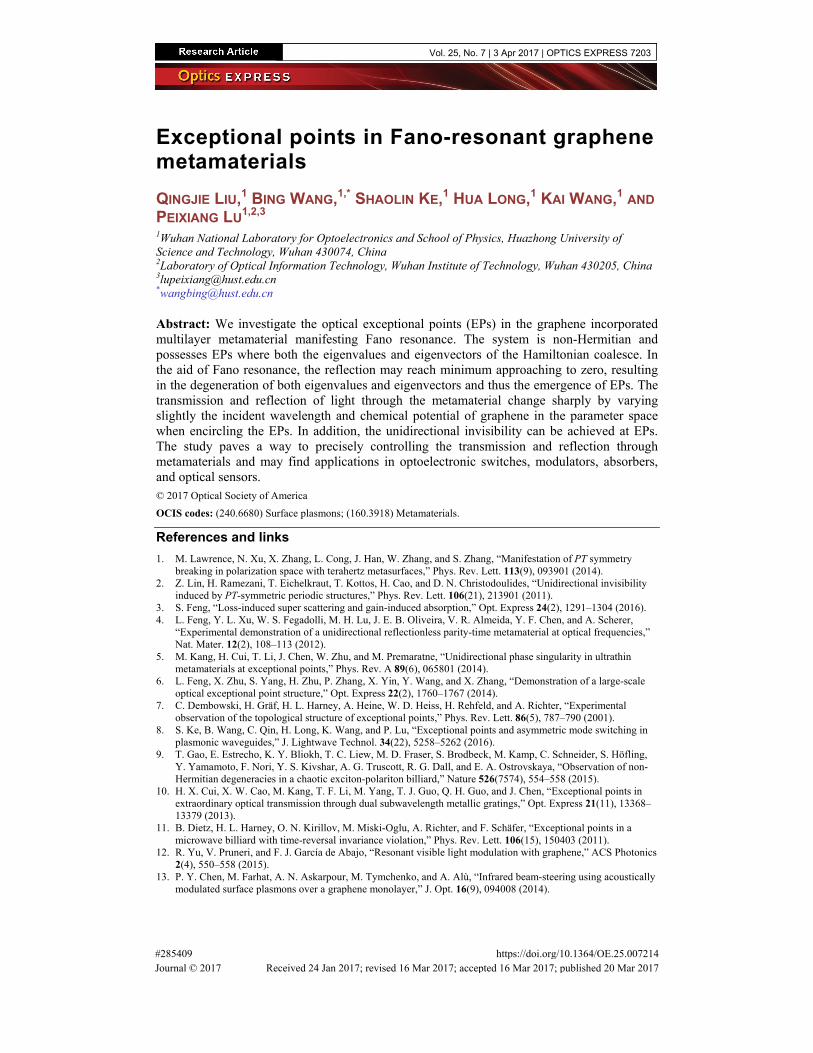
Fig. 2. (a) Transmission for the graphene ribbon arrays suspended in air (the red curve), metallic structure without graphene (the blue curve), and the hybrid structure (the green curve). All parameters are the same as they presented in the hybrid structure. (b) Reflection spectra of the hybrid structure. The chemical potential of graphene is 0.479 eV.
We now focus on the transmission and reflection properties of the metamaterial. The green curve in Fig. 2(a) shows the transmission spectrum of the hybrid metamaterial with both metal gratings and graphene for μc = 0.479 eV. The calculation is performed by using the rigorous coupled wave analysis (RCWA) method [31], which is repeatedly validated in resolving grating problems accurately. There is obviously a sharp drop at λ = 5.346 μm, which is exactly the Fano resonance generated by the interaction between the surface plasmon resonance mode of graphene and the waveguide-resonance mode induced by the current densities flowing parallel to the slits walls of metals [32]. Since the proposed metamaterial is asymmetric in the z direction, the reflections R1 and R2 for light impinging from the top and bottom should be different. Figure 2(b) shows the reflection spectra of the hybrid metamaterial with both metals and graphene, from which we can see clearly that the reflections R1 and R2 are not identical. Both the spectra R1 and R2 have two valleys with one nearly approaching to zero. The near zero points are evidently caused by the Fano resonance, which influence both the transmission and reflection spectra. The EPs should locate at the valleys due to the zero reflection and can be confirmed by tuning the wavelength of incident wave and chemical potential of graphene. In terms of the scaling law, the structure can also operate at larger wavelength by enlarging the geometric parameters. For shorter wavelength, the interband transition may occur and graphene may not support surface plasmons.
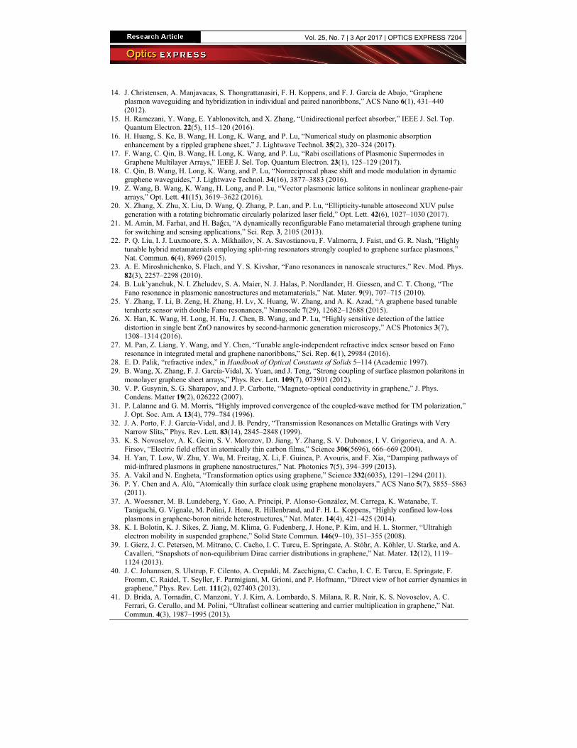
Next we show how to find the EPs. Figure 3(a) plots the reflection spectra R1 as a function of the incident wavelength and graphene chemical potential. A nadir can be observed at μc = 0.428 eV and λ = 5.346 μm. The reflection arrives at R1 = 4.6 × 10⁻⁷ which is fairly equal to zero within the calculation accuracy. Moreover, as shown in Fig. 3(b), the dislocation of
Vol. 25, No. 7 | 3 Apr 2017 | OPTICS EXPRESS 7207
phase φ1 around the nadir point implies that a sharp change of the phase in the vicinity of the EP as the wavelength and chemical potential undergoes a slight variation. In case the light is impinging from the bottom, the reflection spectra R2 as a function of the wavelength and chemical potential is shown in Fig. 3(c). A nadir at μc = 0.479 eV and λ = 5.53 μm is also found, where reflection R2 equals 2.75 × 10⁻⁷ in our calculation. And the phase dislocation of φ2 (Fig. 3(d)) at the nadir point indicates another EP. Thus two EPs are identified at different incident wavelength and chemical potential of graphene, denoted by μc1,2 and λ1,2. It is worth noting that the relaxation time τ ranges between 0.4 ps and 0.5 ps when chemical potential μc is calculated from 0.4 eV to 0.5 eV since the mobility is chosen as 10 000 cm2V−1s−1. This scope of relaxation time is in accordance with simulation [34–36] and has been experimentally realized [37]. We have also investigated the influence of the mobility on EPs. In our calculation, as the mobility decreases to 7000 cm2V−1s−1, that is τ decreases to range between 0.28 ps and 0.35 ps as μc still being from 0.4 eV to 0.5 eV, the EPs can still be observed. The positions of two EPs keep unchanged by comparing with the case of mobility μ = 10 000 cm2V−1s−1. The reason lies in the fact that the relaxation time or mobility can only influence the Q-factor rather than the wavelength of the resonance. In fact, the mobility of graphene used in our work is in accordance with the experimental result [30]. Although the substrate will reduce a lot the mobility, it is possible to fabricate a spacer film between graphene and the substrate. For example, Bolotin et al. have experimentally demonstrated that the mobility can reach 60 000 cm2V−1s−1 for graphene on boron nitride [38]. The spacer film of BN is supposed to restrain the reduction of mobility.
Fig. 3. (a) Reflection spectra R1 and (c) reflection spectra R2 as a function of the incident wavelength λ and chemical potential of graphene μc. (b) and (d) show the reflection phase φ1 and φ2. The black arrows point to the positions of EPs.
In addition, the position of EPs can be shifted by changing all the parameters concerned. When the chemical potential of graphene at EPs increases, the resonance peak of graphene ribbon will undergo a blue shift. To guarantee the Fano resonance, the height of the metallic strips should decrease. On the contrary, the height should increase. For example, when the height becomes h1 = 240 nm and h2 = 165 nm, the EPs can be observed at μc = 0.419 eV, λ = 5.458 μm and μc = 0.46 eV, λ = 5.64 μm, respectively. It should be mentioned that the chemical potential cannot be lower than 0.2 eV because at which the relaxation time is lower
Vol. 25, No. 7 | 3 Apr 2017 | OPTICS EXPRESS 7208

than 0.2 ps [39–41]. The lower relaxation time will be detrimental to the surface plasmon resonance of graphene ribbons.
3. Topological structure of EPs
To further verify the EPs, the topological structure has also been investigated. Figures 4(a) and 4(b) illustrate the real and imaginary parts of eigenvalues as a function of the incident wavelength λ and chemical potential of graphene μc in the vicinity of EP1 and EP2. There are two surfaces in each figure corresponding to the two eigenvalues, that is, the Riemann surface in the parameter space constituted by μc and λ. Since the transmission coefficients t and radicand (r1r2)
1/2 share the similar change trend, the eigenvalues equaling the summation and difference between them manifest very different shape of Riemann surface. The upper surface suffers significantly more prominent curvatures while the lower is comparatively flat. At EP1, as indicated by black arrows in Fig. 4(a) and 4(b), the real and imaginary parts of two eigenvalues coalesce simultaneously. It is the same to EP2, as indicated also in Figs. 4(a) and 4(b). The coalescence for the real and imaginary parts of two eigenvalues suggests the degeneracy of eigenvalues, which is the basic property of EPs.
In the vicinity of EPs, the Riemann surfaces experience crossing or anti-crossing. As far as EP1 is concerned, when μc < μc1, the eigenvalues as a function of wavelength λ show level crossing in the real parts and anti-crossing in the imaginary parts. When μc > μc1, however, they show anti-crossing in the real parts and crossing in the imaginary parts. While in the vicinity of EP2, the eigenvalues as a function of wavelength λ show level anti-crossing in the real parts and crossing in the imaginary parts when μc < μc1. When μc > μc1, the eigenvalues show level crossing in the real parts and anti-crossing in the imaginary parts. The position of level crossing has been denoted by red curves in Fig. 4 in the vicinity of EPs.
Fig. 4. Eigenvalues s1,2 as a function of incident wavelength λ and chemical potential of graphene μc. Re(s) indicates the real parts of s1,2, and Im(s) indicates the imaginary parts of s1,2. The red curves indicate the intersection of two surfaces. The black arrows point to the positions of EP1 and EP2.
Another feature of the topological structure is examined when encircling the EPs in the parameter space constituted by the wavelength λ and chemical potential μc. As shown by the blue loop in Fig. 5(a), only one EP is encircled within a loop in the parameter space. While the system parameters change in the clockwise direction along the loop from the initial position A, the trajectories of real and imaginary parts of eigenvalues are depicted in Figs. 5(b) and 5(c), respectively. After a whole loop, the real and imaginary parts of the eigenvalues exchange to each other. Additionally, the eigenvalues will return back to their initial values after two loops through the same direction of encircling. The result is different when two EPs are encircled within the same loop in the parameter space. As shown in Fig. 5(a), a red loop starting from point B encircles both EP1 and EP2. As the parameters change along the loop in the clockwise direction, the evolution of real part of eigenvalues s1,2 is plotted in Fig. 5(d). After a loop, the real parts of two eigenvalues return to their original
Vol. 25, No. 7 | 3 Apr 2017 | OPTICS EXPRESS 7209
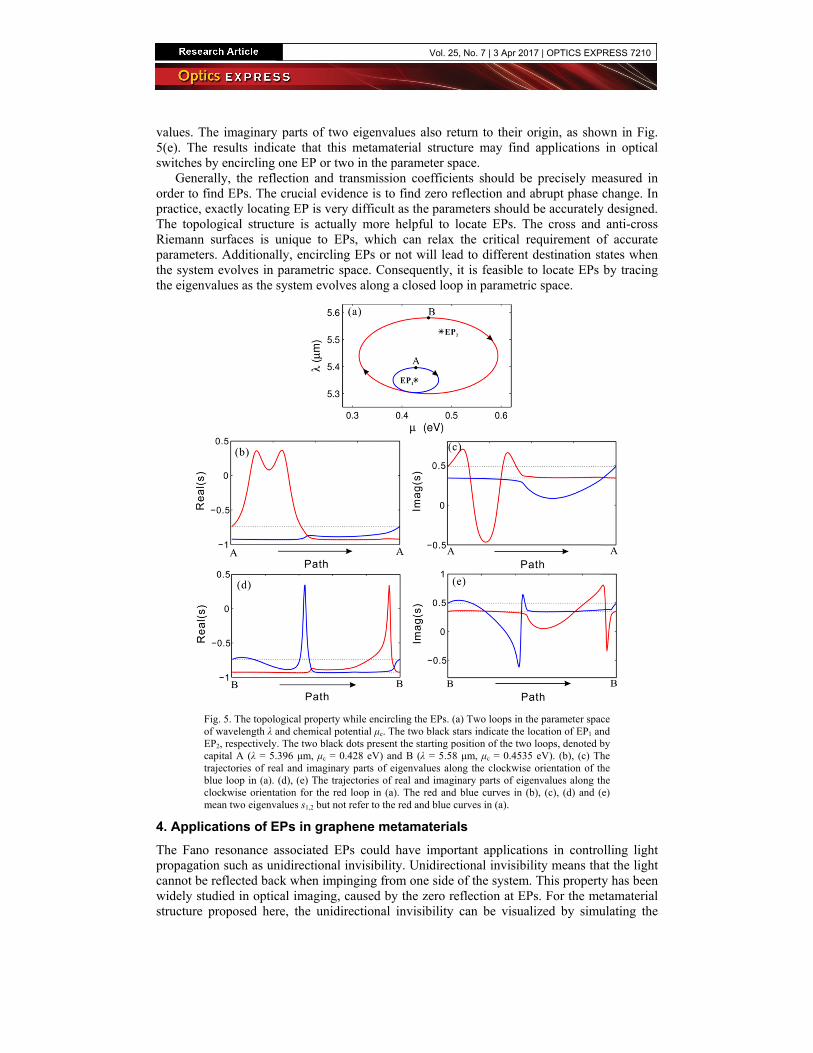
values. The imaginary parts of two eigenvalues also return to their origin, as shown in Fig. 5(e). The results indicate that this metamaterial structure may find applications in optical switches by encircling one EP or two in the parameter space.
Generally, the reflection and transmission coefficients should be precisely measured in order to find EPs. The crucial evidence is to find zero reflection and abrupt phase change. In practice, exactly locating EP is very difficult as the parameters should be accurately designed. The topological structure is actually more helpful to locate EPs. The cross and anti-cross Riemann surfaces is unique to EPs, which can relax the critical requirement of accurate parameters. Additionally, encircling EPs or not will lead to different destination states when the system evolves in parametric space. Consequently, it is feasible to locate EPs by tracing the eigenvalues as the system evolves along a closed loop in parametric space.
Fig. 5. The topological property while encircling the EPs. (a) Two loops in the parameter space of wavelength λ and chemical potential μc. The two black stars indicate the location of EP1 and EP2, respectively. The two black dots present the starting position of the two loops, denoted by capital A (λ = 5.396 μm, μc = 0.428 eV) and B (λ = 5.58 μm, μc = 0.4535 eV). (b), (c) The trajectories of real and imaginary parts of eigenvalues along the clockwise orientation of the blue loop in (a). (d), (e) The trajectories of real and imaginary parts of eigenvalues along the clockwise orientation for the red loop in (a). The red and blue curves in (b), (c), (d) and (e) mean two eigenvalues s1,2 but not refer to the red and blue curves in (a).
4. Applications of EPs in graphene metamaterials
The Fano resonance associated EPs could have important applications in controlling light propagation such as unidirectional invisibility. Unidirectional invisibility means that the light cannot be reflected back when impinging from one side of the system. This property has been widely studied in optical imaging, caused by the zero reflection at EPs. For the metamaterial structure proposed here, the unidirectional invisibility can be visualized by simulating the
Vol. 25, No. 7 | 3 Apr 2017 | OPTICS EXPRESS 7210
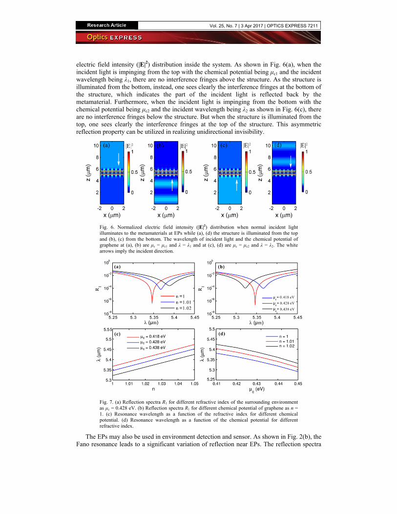
electric field intensity (|E|2) distribution inside the system. As shown in Fig. 6(a), when the incident light is impinging from the top with the chemical potential being μc1 and the incident wavelength being λ1, there are no interference fringes above the structure. As the structure is illuminated from the bottom, instead, one sees clearly the interference fringes at the bottom of the structure, which indicates the part of the incident light is reflected back by the metamaterial. Furthermore, when the incident light is impinging from the bottom with the chemical potential being μc2 and the incident wavelength being λ2 as shown in Fig. 6(c), there are no interference fringes below the structure. But when the structure is illuminated from the top, one sees clearly the interference fringes at the top of the structure. This asymmetric reflection property can be utilized in realizing unidirectional invisibility.
Fig. 6. Normalized electric field intensity (|E|2) distribution when normal incident light illuminates to the metamaterials at EPs while (a), (d) the structure is illuminated from the top and (b), (c) from the bottom. The wavelength of incident light and the chemical potential of graphene at (a), (b) are μc = μc1 and λ = λ1 and at (c), (d) are μc = μc2 and λ = λ2. The white arrows imply the incident direction.
Fig. 7. (a) Reflection spectra R1 for different refractive index of the surrounding environment as μc = 0.428 eV. (b) Reflection spectra R1 for different chemical potential of graphene as n = 1. (c) Resonance wavelength as a function of the refractive index for different chemical potential. (d) Resonance wavelength as a function of the chemical potential for different refractive index.
The EPs may also be used in environment detection and sensor. As shown in Fig. 2(b), the Fano resonance leads to a significant variation of reflection near EPs. The reflection spectra
Vol. 25, No. 7 | 3 Apr 2017 | OPTICS EXPRESS 7211
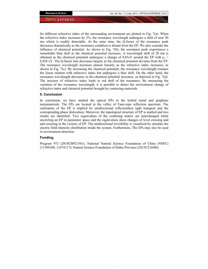
for different refractive index of the surrounding environment are plotted in Fig. 7(a). When the refractive index increases by 2%, the resonance wavelength undergoes a shift of near 50 nm which is readily detectable. At the same time, the Q-factor of the resonance peak decreases dramatically as the resonance condition is distant from the EP. We also consider the influence of chemical potential. As shown in Fig. 7(b), the resonance peak experiences a remarkable blue shift as the chemical potential increases. A wavelength shift of 20 nm is obtained as the chemical potential undergoes a change of 0.01eV around the EP with μc = 0.428 eV. The Q-factor also decreases largely as the chemical potential deviates from the EP. The resonance wavelength increases almost linearly as the refractive index increases, as shown in Fig. 7(c). By increasing the chemical potential, the resonance wavelength remains the linear relation with refractive index but undergoes a blue shift. On the other hand, the resonance wavelength decreases as the chemical potential increases, as depicted in Fig. 7(d). The increase of refractive index leads to red shift of the resonance. By measuring the variation of the resonance wavelength, it is possible to detect the environment change of refractive index and chemical potential brought by contacting materials.
5. Conclusion
In conclusion, we have studied the optical EPs in the hybrid metal and graphene metamaterials. The EPs are located at the valley of Fano-type reflection spectrum. The realization of the EP is implied by unidirectional reflectionless light transport and the corresponding phase dislocation. Moreover, the topological structure of EP is studied and two results are identified. Two eigenvalues of the scattering matrix are interchanged while encircling an EP in parameter space and the eigenvalues show changes of level crossing and anti-crossing in the vicinity of EP. The unidirectional invisibility is visualized by simulate the electric field intensity distribution inside the system. Furthermore, The EPs may also be used in environment detection.
Funding
Program 973 (2014CB921301); National Natural Science Foundation of China (NSFC) (11304108, 11674117); Natural Science Foundation of Hubei Province (2015CFA040).
Vol. 25, No. 7 | 3 Apr 2017 | OPTICS EXPRESS 7212