experiment 6: frequency modulation (fm), generation and...
TRANSCRIPT
Experiment 6: Frequency Modulation (FM), Generation and Detection By: Prof. Gabriel M. Rebeiz EECS Dept. The University of Michigan [email protected]
Equipment Required • Agilent E3631A Triple output DC power supply
• Agilent 33120A Function Generator
• Agilent 34401A Multimeter
• Written for Agilent 54645A Oscilloscope (could substitute 54622A Oscilloscope)
• 6.1 Treble Tone Control Amplifier:
1.0 Frequency Modulation Frequency modulation (FM) is the standard technique for high-fidelity communications as is evident in the received signals of the FM band (88-108 MHz) vs. the AM band (450-1650 KHz). The main reason for the improved fidelity is that FM detectors, when properly designed, are not sensitive to random amplitude variations which are the dominant part of electrical noise (heard as static on the AM radio). Frequency modulation is not only used in commercial radio broadcasts, but also in police and hospital communications, emergency channels, TV sound, wireless (cellular) telephone systems, and radio amateur bands above 30 MHz. The basic idea of an FM signal vs. an AM signal is shown in Fig. 1. In an FM signal, the frequency of the signal is changed by the modulation (baseband) signal while its amplitude remains the same. In an AM signal, we now know that it is the amplitude (or the envelope) of the signal that is changed by the modulation signal. The FM signal can be summarized as follows:
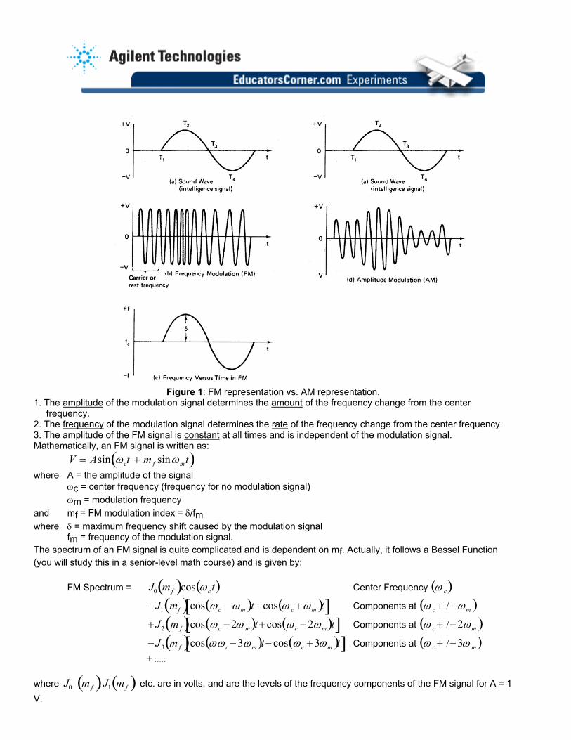
Figure 1: FM representation vs. AM representation.
1. The amplitude of the modulation signal determines the amount of the frequency change from the center frequency.
2. The frequency of the modulation signal determines the rate of the frequency change from the center frequency. 3. The amplitude of the FM signal is constant at all times and is independent of the modulation signal. Mathematically, an FM signal is written as: V = Asin ωct + mf sinωmt( ) where A = the amplitude of the signal ωc = center frequency (frequency for no modulation signal) ωm = modulation frequency and mf = FM modulation index = δ/fm where δ = maximum frequency shift caused by the modulation signal fm = frequency of the modulation signal. The spectrum of an FM signal is quite complicated and is dependent on mf. Actually, it follows a Bessel Function (you will study this in a senior-level math course) and is given by:
FM Spectrum = Center Frequency J0 mf( )cos ωct( ) ω c( )
−J1 mf( ) cos ωc −ωm( )t−cos ω c+ωm( )t[ ] Components at ω c+ /−ωm( )
+J2 mf( )cos ωc −2ω m( )t+cos ωc −2ωm( )t[ ] Components at ω c+ /−2ωm( )
−J3 mf( )cos ωωc−3ωm( )t−cos ωc +3ωm( )t[ ] Components at ω c+ /−3ω m( ) + .....
where etc. are in volts, and are the levels of the frequency components of the FM signal for A = 1 V.
J0 mf( ), J1 mf( )

The spectrum is dependent on mf, the modulation index, and Table 1 gives the values of the Bessel-functions J0, J1, J2, etc.... for mf = 0 to 15. Figure 2 gives some spectrum representation for various modulation indices. Notice from Table 1 that for mf = 2.4, there is no power in the center frequency component (J0(2.4) =0). This also occurs at mf = 5.5, 8.6, ... . This does not mean that there is no power transmitted in the signal. All that it means is that for m = 2.4, 5.5, ..., there is no power at the center frequency and all of the power is in the sidebands.
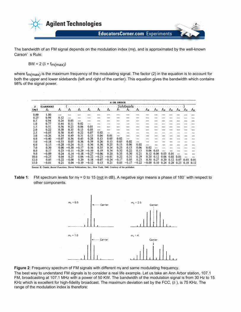
The bandwidth of an FM signal depends on the modulation index (mf), and is approximated by the well-known Carson’ s Rule: BW = 2 (δ + fm(max)) where fm(max) is the maximum frequency of the modulating signal. The factor (2) in the equation is to account for both the upper and lower sidebands (left and right of the carrier). This equation gives the bandwidth which contains 98% of the signal power.
Table 1: FM spectrum levels for mf = 0 to 15 (not in dB). A negative sign means a phase of 180˚ with respect to
other components.
Figure 2: Frequency spectrum of FM signals with different mf and same modulating frequency. The best way to understand FM signals is to consider a real life example. Let us take an Ann Arbor station, 107.1 FM, broadcasting at 107.1 MHz with a power of 50 KW. The bandwidth of the modulation signal is from 30 Hz to 15 KHz which is excellent for high-fidelity broadcast. The maximum deviation set by the FCC, (δ ), is 75 KHz. The range of the modulation index is therefore:
mf(min) = δ/fm(max) = 75 KHz/15 KHz= 5 (for fm= 15 KHz) to mf(max) = δ/fm(min) = 75 KHz/30 Hz = 2500! (for fm= 30 Hz) Notice that the modulation index changes a lot with the modulation frequency (from 2,500 to 5). For the 15 KHz signal, mf = 5 and from Table 1, we see that the frequency components are up high up to J6 and drop quickly afterwards. This means that the bandwidth of the signal is 6x15 KHz = 90 KHz on each side of the center frequency (a total bandwidth of 180 KHz). We can also use Carson’s rule and, BW = 2 (δ + fm(max)) = 180 KHz or 90 KHz on each side of the center frequency. For the 30 Hz signal and mf = 2,500, a huge number of sidebands exist but remember that there are now spaced at only 30 Hz apart. The total bandwidth of the signal is BW = 2 (δ+ fm(min)) = 150 KHz or 75 KHz on each side of the center frequency. This means that the bandwidth of the FM signal changes from +/- 75 KHz to +/- 90 KHz from the carrier depending on the modulation frequency.
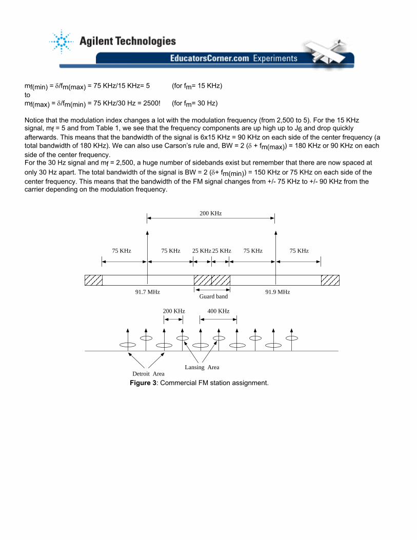
75 KHz 75 KHz 25 KHz 25 KHz 75 KHz75 KHz
91.9 MHz91.7 MHz
200 KHz
Detroit AreaLansing Area
200 KHz
Guard band
400 KHz
Figure 3: Commercial FM station assignment.
Commercial FM stations are therefore spaced 200 KHz apart to avoid interference for all modulating frequencies. In order to even isolate the stations further, FCC only assigns alternate stations for a certain area. For example, in the Detroit/Ann Arbor area, the stations are 107.1, 107.5 (and 93.1, 93.5, 93.9, ...) spaced 400 KHz apart. In adjoining areas, such as Toledo to the south (or Lansing to the north, but very far from Toledo), the stations are also centered at 400 KHz, but they are 107.3, 107.7, etc... (and 93.3, 93.7, 94.1 etc...). This allows inexpensive radios with bad-to-acceptable selectivity to receive FM stations without interference from adjoining stations (since they are 400 KHz away and not only 200 KHz away). The 200 KHz-away stations are very far and therefore their signals would appear as noise in the receiver. However, as mentioned before, FM receivers have excellent noise rejection and therefore are not affected by the far-away stations.
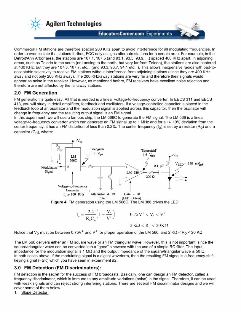
2.0 FM Generation FM generation is quite easy. All that is needed is a linear voltage-to-frequency converter. In EECS 311 and EECS 413, you will study in detail amplifiers, feedback and oscillators. If a voltage-controlled capacitor is placed in the feedback loop of an oscillator and the modulation signal is applied across this capacitor, then the oscillator will change in frequency and the resulting output signal is an FM signal. In this experiment, we will use a famous chip, the LM 566C to generate the FM signal. The LM 566 is a linear voltage-to-frequency converter which can generate an FM signal up to 1 MHz and for a +/- 10% deviation from the center frequency, it has an FM distortion of less than 0.2%. The center frequency (fo) is set by a resistor (Ro) and a capacitor (Co), where:
Figure 4: FM generation using the LM 566C. The LM 386 drives the LED.
fo = 2.4RoCo
1 − V5
V+
0.75V + < V5 < V+
2 KΩ < Ro < 20KΩ
Notice that V5 must be between 0.75V+ and V+ for proper operation of the LM 566, and 2 KΩ < Ro < 20 KΩ.
The LM 566 delivers either an FM square wave or an FM triangular wave. However, this is not important, since the square/triangular wave can be converted into a “good” sinewave with the use of a simple RC filter. The input impedance for the modulation signal is 1 MΩ and the output impedance of the square/triangular wave is 50 Ω. In both cases above, if the modulating signal is a digital waveform, then the resulting FM signal is a frequency-shift-keying signal (FSK) which you have seen in experiment #2.
3.0 FM Detection (FM Discriminators): FM detection is the secret for the success of FM broadcasts. Basically, one can design an FM detector, called a frequency discriminator, which is immune to any amplitude variations (noise) in the signal. Therefore, it can be used with weak signals and can reject strong interfering stations. There are several FM discriminator designs and we will cover some of them below. 1. Slope Detector:
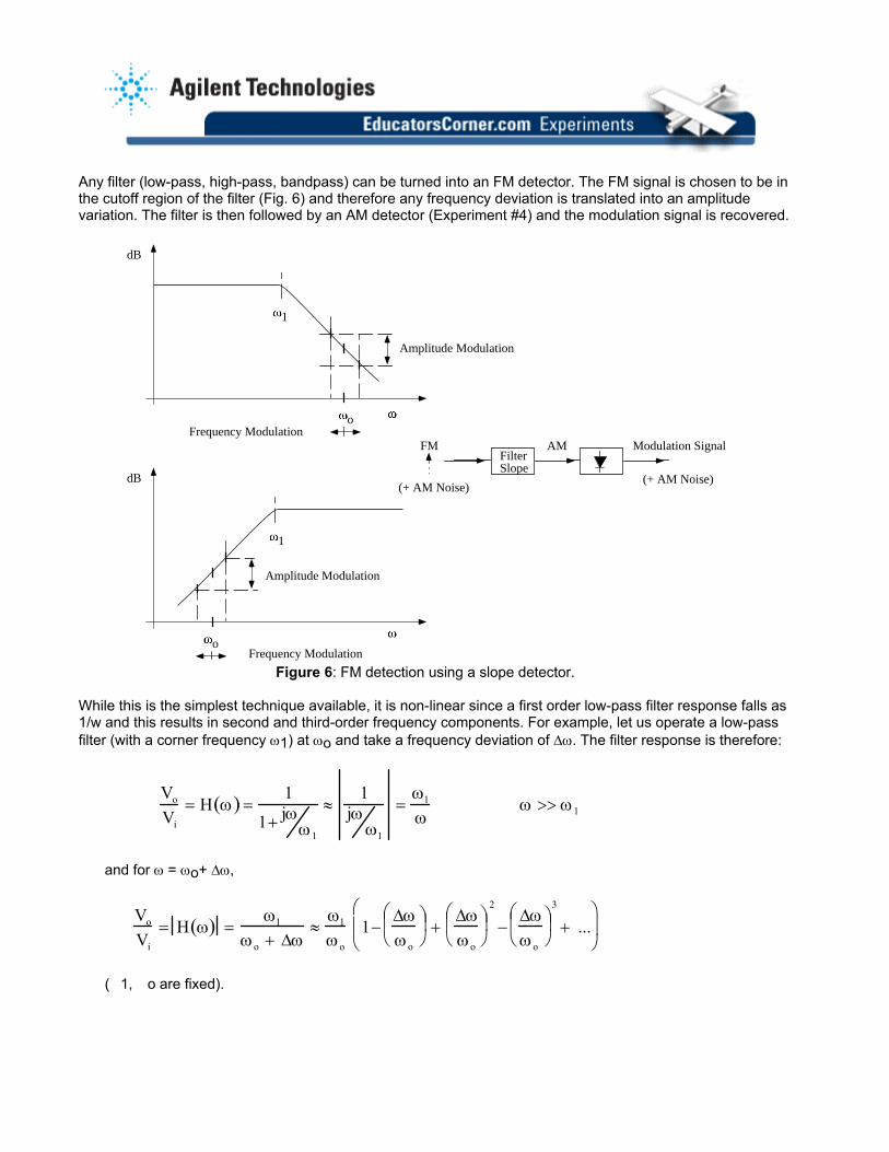
Any filter (low-pass, high-pass, bandpass) can be turned into an FM detector. The FM signal is chosen to be in the cutoff region of the filter (Fig. 6) and therefore any frequency deviation is translated into an amplitude variation. The filter is then followed by an AM detector (Experiment #4) and the modulation signal is recovered.
dB
o
1
Amplitude Modulation
Frequency Modulation
dB
o
1
Amplitude Modulation
Frequency Modulation
FilterSlope
AM Modulation Signal
(+ AM Noise)(+ AM Noise)
FM
Figure 6: FM detection using a slope detector.
While this is the simplest technique available, it is non-linear since a first order low-pass filter response falls as 1/w and this results in second and third-order frequency components. For example, let us operate a low-pass filter (with a corner frequency ω1) at ωo and take a frequency deviation of ∆ω. The filter response is therefore:
Vo
Vi
= H ω( ) =1
1+ jωω1
≈1
jωω1
=ω1
ωω >> ω1
and for ω = ωo+ ∆ω,
Vo
Vi
= H ω( ) =ω1
ωo + ∆ω≈
ω1
ωo
1−∆ωωo
+
∆ωωo
2
−∆ωωo
3
+ ...
(1, o are fixed).
The peak of the envelope occurs for a negative ∆ω and is Viω1
ωo
1 +
∆ωωo
. The minimum of the
envelope occurs for a positive ∆ω and is Viω1
ωo
1 −
∆ωωo
. Therefore, the AM modulation factor, m, is
∆ω ωo for a first-order slope detector.
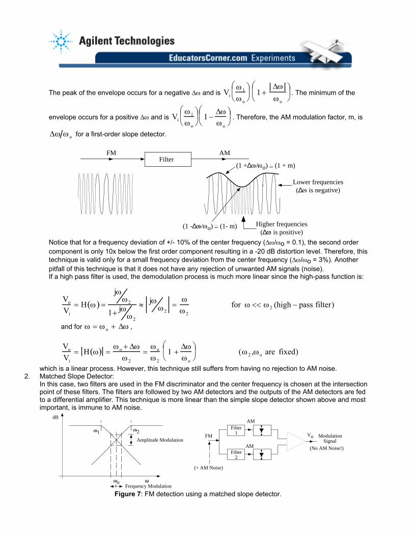
AMFMFilter
(1 +∆ / o) (1 + m)
(1 -∆ / o) (1- m) Higher frequencies(∆ is positive)
Lower frequencies(∆ is negative)
Notice that for a frequency deviation of +/- 10% of the center frequency (∆ω/ωo = 0.1), the second order component is only 10x below the first order component resulting in a -20 dB distortion level. Therefore, this technique is valid only for a small frequency deviation from the center frequency (∆ω/ωo = 3%). Another pitfall of this technique is that it does not have any rejection of unwanted AM signals (noise).
If a high pass filter is used, the demodulation process is much more linear since the high-pass function is:
Vo
Vi
= H ω( ) =
jωω2
1+ jωω2
≈ jωω2
=ω
ω2
for ω << ω2 (high − pass filter)
and for , ω = ωo + ∆ω
Vo
Vi
= H ω( ) =ωo + ∆ω
ω2
=ωo
ω2
1 +∆ωωo
(ω2 ,ωo are fixed)
which is a linear process. However, this technique still suffers from having no rejection to AM noise. 2. Matched Slope Detector:
dB
o
1
Amplitude Modulation
Frequency Modulation
(+ AM Noise)
Filter1
AM
Modulation Signal
(No AM Noise!)
FM
Filter2
AM +
-2
Vo
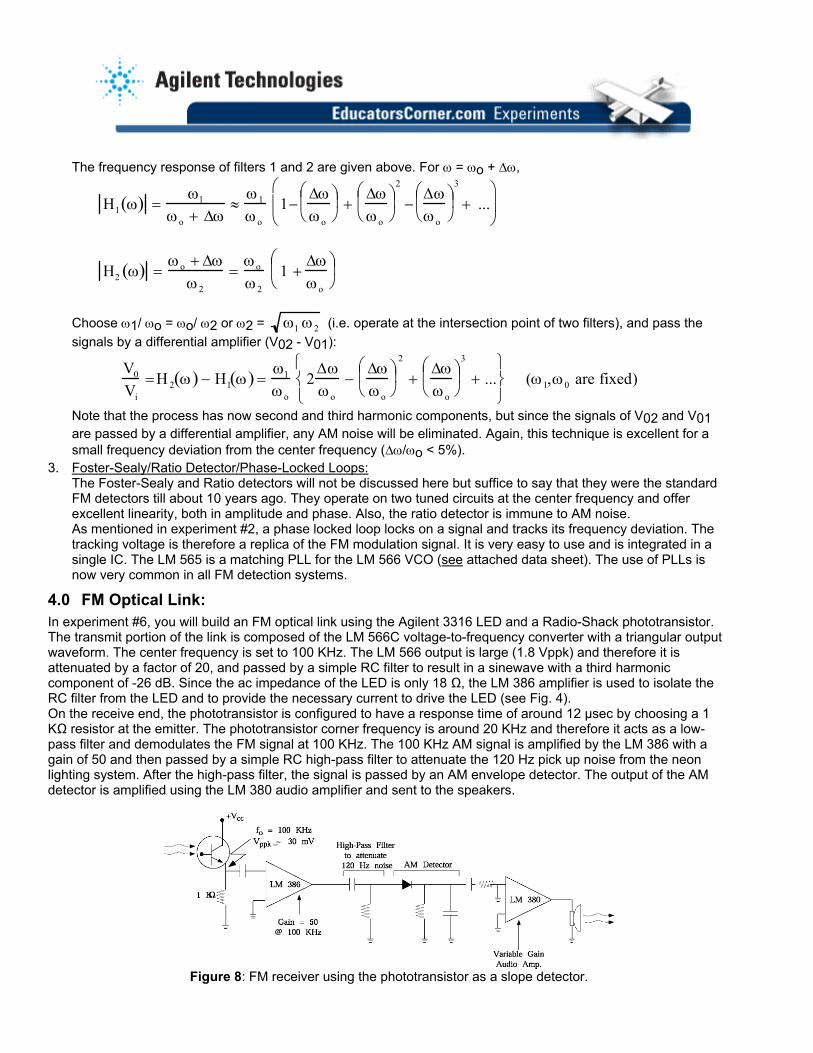
In this case, two filters are used in the FM discriminator and the center frequency is chosen at the intersection point of these filters. The filters are followed by two AM detectors and the outputs of the AM detectors are fed to a differential amplifier. This technique is more linear than the simple slope detector shown above and most important, is immune to AM noise.
Figure 7: FM detection using a matched slope detector.
The frequency response of filters 1 and 2 are given above. For ω = ωo + ∆ω,
H1 ω( ) =ω1
ωo + ∆ω≈
ω1
ωo
1−∆ωωo
+
∆ωωo
2
−∆ωωo
3
+ ...
H2 ω( ) =ωo + ∆ω
ω2
=ωo
ω2
1 +∆ωωo
Choose ω1/ ωo = ωo/ ω2 or ω2 = ω1 ω2 (i.e. operate at the intersection point of two filters), and pass the signals by a differential amplifier (V02 - V01):
V0
Vi
=H 2 ω( ) − H1 ω( ) =ω1
ωo
2∆ωωo
−∆ωωo
2
+∆ωωo
3
+ ...
(ω1,ω0 are fixed)
Note that the process has now second and third harmonic components, but since the signals of V02 and V01 are passed by a differential amplifier, any AM noise will be eliminated. Again, this technique is excellent for a small frequency deviation from the center frequency (∆ω/ωo < 5%).
3. Foster-Sealy/Ratio Detector/Phase-Locked Loops: The Foster-Sealy and Ratio detectors will not be discussed here but suffice to say that they were the standard
FM detectors till about 10 years ago. They operate on two tuned circuits at the center frequency and offer excellent linearity, both in amplitude and phase. Also, the ratio detector is immune to AM noise.
As mentioned in experiment #2, a phase locked loop locks on a signal and tracks its frequency deviation. The tracking voltage is therefore a replica of the FM modulation signal. It is very easy to use and is integrated in a single IC. The LM 565 is a matching PLL for the LM 566 VCO (see attached data sheet). The use of PLLs is now very common in all FM detection systems.
4.0 FM Optical Link: In experiment #6, you will build an FM optical link using the Agilent 3316 LED and a Radio-Shack phototransistor. The transmit portion of the link is composed of the LM 566C voltage-to-frequency converter with a triangular output waveform. The center frequency is set to 100 KHz. The LM 566 output is large (1.8 Vppk) and therefore it is attenuated by a factor of 20, and passed by a simple RC filter to result in a sinewave with a third harmonic component of -26 dB. Since the ac impedance of the LED is only 18 Ω, the LM 386 amplifier is used to isolate the RC filter from the LED and to provide the necessary current to drive the LED (see Fig. 4). On the receive end, the phototransistor is configured to have a response time of around 12 µsec by choosing a 1 KΩ resistor at the emitter. The phototransistor corner frequency is around 20 KHz and therefore it acts as a low-pass filter and demodulates the FM signal at 100 KHz. The 100 KHz AM signal is amplified by the LM 386 with a gain of 50 and then passed by a simple RC high-pass filter to attenuate the 120 Hz pick up noise from the neon lighting system. After the high-pass filter, the signal is passed by an AM envelope detector. The output of the AM detector is amplified using the LM 380 audio amplifier and sent to the speakers.
Figure 8: FM receiver using the phototransistor as a slope detector.
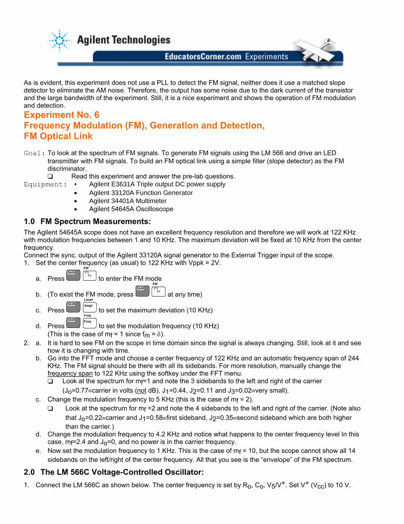
As is evident, this experiment does not use a PLL to detect the FM signal, neither does it use a matched slope detector to eliminate the AM noise. Therefore, the output has some noise due to the dark current of the transistor and the large bandwidth of the experiment. Still, it is a nice experiment and shows the operation of FM modulation and detection. Experiment No. 6 Frequency Modulation (FM), Generation and Detection, FM Optical Link Goal: To look at the spectrum of FM signals. To generate FM signals using the LM 566 and drive an LED
transmitter with FM signals. To build an FM optical link using a simple filter (slope detector) as the FM discriminator. Read this experiment and answer the pre-lab questions.
Equipment: • Agilent E3631A Triple output DC power supply • Agilent 33120A Function Generator • Agilent 34401A Multimeter • Agilent 54645A Oscilloscope
1.0 FM Spectrum Measurements: The Agilent 54645A scope does not have an excellent frequency resolution and therefore we will work at 122 KHz with modulation frequencies between 1 and 10 KHz. The maximum deviation will be fixed at 10 KHz from the center frequency. Connect the sync. output of the Agilent 33120A signal generator to the External Trigger input of the scope. 1. Set the center frequency (as usual) to 122 KHz with Vppk = 2V.
a. Press Shift
FM
to enter the FM mode
b. (To exist the FM mode, press Shift
FM
at any time)
c. Press Shift
Ampl
Level
to set the maximum deviation (10 KHz)
d. Press Shift
Freq
Freq
to set the modulation frequency (10 KHz) (This is the case of mf = 1 since fm = δ). 2. a. It is hard to see FM on the scope in time domain since the signal is always changing. Still, look at it and see
how it is changing with time. b. Go into the FFT mode and choose a center frequency of 122 KHz and an automatic frequency span of 244
KHz. The FM signal should be there with all its sidebands. For more resolution, manually change the frequency span to 122 KHz using the softkey under the FFT menu.
Look at the spectrum for mf=1 and note the 3 sidebands to the left and right of the carrier (Jo=0.77≡carrier in volts (not dB), J1=0.44, J2=0.11 and J3=0.02≡very small).
c. Change the modulation frequency to 5 KHz (this is the case of mf = 2). Look at the spectrum for mf =2 and note the 4 sidebands to the left and right of the carrier. (Note also
that Jo=0.22≡carrier and J1=0.58≡first sideband, J2=0.35≡second sideband which are both higher than the carrier.)
d. Change the modulation frequency to 4.2 KHz and notice what happens to the center frequency level In this case, mf=2.4 and Jo=0, and no power is in the carrier frequency.
e. Now set the modulation frequency to 1 KHz. This is the case of mf = 10, but the scope cannot show all 14 sidebands on the left/right of the center frequency. All that you see is the “envelope” of the FM spectrum.
2.0 The LM 566C Voltage-Controlled Oscillator: 1. Connect the LM 566C as shown below. The center frequency is set by Ro, Co, V5/V+. Set V+ (Vcc) to 10 V.
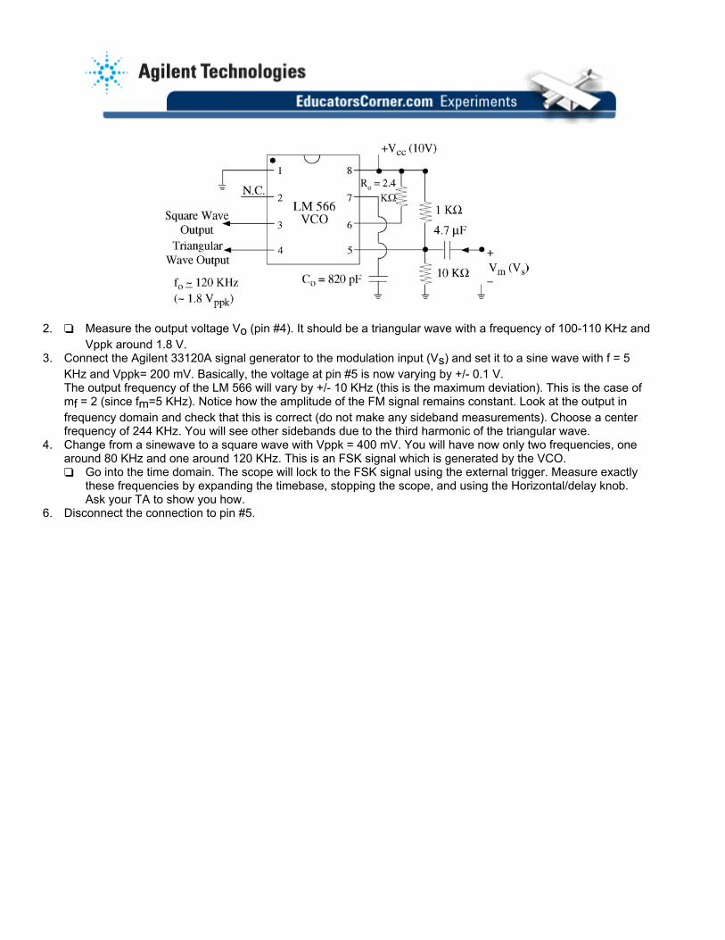
2. Measure the output voltage Vo (pin #4). It should be a triangular wave with a frequency of 100-110 KHz and
Vppk around 1.8 V. 3. Connect the Agilent 33120A signal generator to the modulation input (Vs) and set it to a sine wave with f = 5
KHz and Vppk= 200 mV. Basically, the voltage at pin #5 is now varying by +/- 0.1 V. The output frequency of the LM 566 will vary by +/- 10 KHz (this is the maximum deviation). This is the case of mf = 2 (since fm=5 KHz). Notice how the amplitude of the FM signal remains constant. Look at the output in frequency domain and check that this is correct (do not make any sideband measurements). Choose a center frequency of 244 KHz. You will see other sidebands due to the third harmonic of the triangular wave.
4. Change from a sinewave to a square wave with Vppk = 400 mV. You will have now only two frequencies, one around 80 KHz and one around 120 KHz. This is an FSK signal which is generated by the VCO.
Go into the time domain. The scope will lock to the FSK signal using the external trigger. Measure exactly these frequencies by expanding the timebase, stopping the scope, and using the Horizontal/delay knob. Ask your TA to show you how.
6. Disconnect the connection to pin #5.
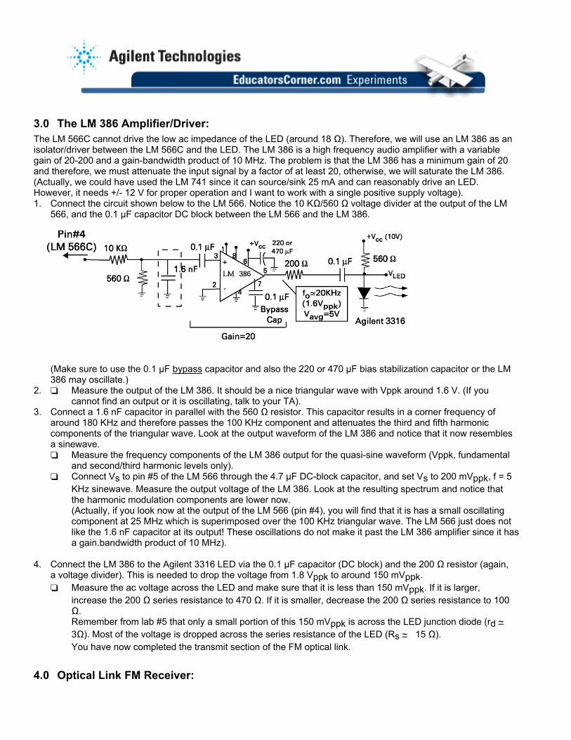
3.0 The LM 386 Amplifier/Driver: The LM 566C cannot drive the low ac impedance of the LED (around 18 Ω). Therefore, we will use an LM 386 as an isolator/driver between the LM 566C and the LED. The LM 386 is a high frequency audio amplifier with a variable gain of 20-200 and a gain-bandwidth product of 10 MHz. The problem is that the LM 386 has a minimum gain of 20 and therefore, we must attenuate the input signal by a factor of at least 20, otherwise, we will saturate the LM 386. (Actually, we could have used the LM 741 since it can source/sink 25 mA and can reasonably drive an LED. However, it needs +/- 12 V for proper operation and I want to work with a single positive supply voltage). 1. Connect the circuit shown below to the LM 566. Notice the 10 KΩ/560 Ω voltage divider at the output of the LM
566, and the 0.1 µF capacitor DC block between the LM 566 and the LM 386.
(Make sure to use the 0.1 µF bypass capacitor and also the 220 or 470 µF bias stabilization capacitor or the LM 386 may oscillate.)
2. Measure the output of the LM 386. It should be a nice triangular wave with Vppk around 1.6 V. (If you cannot find an output or it is oscillating, talk to your TA).
3. Connect a 1.6 nF capacitor in parallel with the 560 Ω resistor. This capacitor results in a corner frequency of around 180 KHz and therefore passes the 100 KHz component and attenuates the third and fifth harmonic components of the triangular wave. Look at the output waveform of the LM 386 and notice that it now resembles a sinewave.
Measure the frequency components of the LM 386 output for the quasi-sine waveform (Vppk, fundamental and second/third harmonic levels only).
Connect Vs to pin #5 of the LM 566 through the 4.7 µF DC-block capacitor, and set Vs to 200 mVppk, f = 5 KHz sinewave. Measure the output voltage of the LM 386. Look at the resulting spectrum and notice that the harmonic modulation components are lower now.
(Actually, if you look now at the output of the LM 566 (pin #4), you will find that it is has a small oscillating component at 25 MHz which is superimposed over the 100 KHz triangular wave. The LM 566 just does not like the 1.6 nF capacitor at its output! These oscillations do not make it past the LM 386 amplifier since it has a gain.bandwidth product of 10 MHz).
4. Connect the LM 386 to the Agilent 3316 LED via the 0.1 µF capacitor (DC block) and the 200 Ω resistor (again,
a voltage divider). This is needed to drop the voltage from 1.8 Vppk to around 150 mVppk. Measure the ac voltage across the LED and make sure that it is less than 150 mVppk. If it is larger,
increase the 200 Ω series resistance to 470 Ω. If it is smaller, decrease the 200 Ω series resistance to 100 Ω.
Remember from lab #5 that only a small portion of this 150 mVppk is across the LED junction diode (rd ~– 3Ω). Most of the voltage is dropped across the series resistance of the LED (Rs ~– 15 Ω).
You have now completed the transmit section of the FM optical link.
4.0 Optical Link FM Receiver:
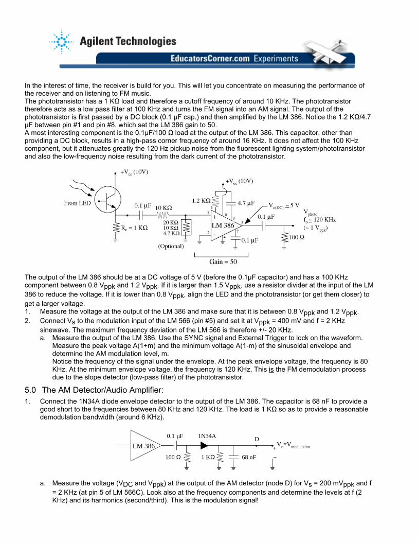
In the interest of time, the receiver is build for you. This will let you concentrate on measuring the performance of the receiver and on listening to FM music. The phototransistor has a 1 KΩ load and therefore a cutoff frequency of around 10 KHz. The phototransistor therefore acts as a low pass filter at 100 KHz and turns the FM signal into an AM signal. The output of the phototransistor is first passed by a DC block (0.1 µF cap.) and then amplified by the LM 386. Notice the 1.2 KΩ/4.7 µF between pin #1 and pin #8, which set the LM 386 gain to 50. A most interesting component is the 0.1µF/100 Ω load at the output of the LM 386. This capacitor, other than providing a DC block, results in a high-pass corner frequency of around 16 KHz. It does not affect the 100 KHz component, but it attenuates greatly the 120 Hz pickup noise from the fluorescent lighting system/phototransistor and also the low-frequency noise resulting from the dark current of the phototransistor.
The output of the LM 386 should be at a DC voltage of 5 V (before the 0.1µF capacitor) and has a 100 KHz component between 0.8 Vppk and 1.2 Vppk. If it is larger than 1.5 Vppk, use a resistor divider at the input of the LM 386 to reduce the voltage. If it is lower than 0.8 Vppk, align the LED and the phototransistor (or get them closer) to get a larger voltage. 1. Measure the voltage at the output of the LM 386 and make sure that it is between 0.8 Vppk and 1.2 Vppk. 2. Connect Vs to the modulation input of the LM 566 (pin #5) and set it at Vppk = 400 mV and f = 2 KHz
sinewave. The maximum frequency deviation of the LM 566 is therefore +/- 20 KHz. a. Measure the output of the LM 386. Use the SYNC signal and External Trigger to lock on the waveform.
Measure the peak voltage A(1+m) and the minimum voltage A(1-m) of the sinusoidal envelope and determine the AM modulation level, m.
Notice the frequency of the signal under the envelope. At the peak envelope voltage, the frequency is 80 KHz. At the minimum envelope voltage, the frequency is 120 KHz. This is the FM demodulation process due to the slope detector (low-pass filter) of the phototransistor.
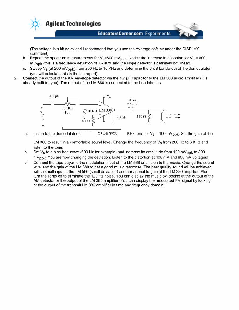
5.0 The AM Detector/Audio Amplifier: 1. Connect the 1N34A diode envelope detector to the output of the LM 386. The capacitor is 68 nF to provide a
good short to the frequencies between 80 KHz and 120 KHz. The load is 1 KΩ so as to provide a reasonable demodulation bandwidth (around 6 KHz).
0.1 µF
100 Ω
Vo=VmodulationLM 386
1 KΩ 68 nF
+–
1N34A D
a. Measure the voltage (VDC and Vppk) at the output of the AM detector (node D) for Vs = 200 mVppk and f
= 2 KHz (at pin 5 of LM 566C). Look also at the frequency components and determine the levels at f (2 KHz) and its harmonics (second/third). This is the modulation signal!
(The voltage is a bit noisy and I recommend that you use the Average softkey under the DISPLAY
command). b. Repeat the spectrum measurements for Vs=800 mVppk. Notice the increase in distortion for Vs = 800
mVppk (this is a frequency deviation of +/- 40% and the slope detector is definitely not linear!). c. Sweep Vs (at 200 mVppk) from 200 Hz to 10 KHz and determine the 3-dB bandwidth of the demodulator
(you will calculate this in the lab report). 2. Connect the output of the AM envelope detector via the 4.7 µF capacitor to the LM 380 audio amplifier (it is
already built for you). The output of the LM 380 is connected to the headphones.
4.7 µFVm
LM 380
560 Ω
100 or220 µF+ –+
–
100 KΩPot. 10 KΩ
10 KΩ
+Vcc
+
–
4.7 µF
5 G a. Listen to the demodulated 2 KHz tone for Vs = 100 mVppk. Set the gain of the
LM 380 to result in a comfortable sound level. Change the frequency of Vs from 200 Hz to 6 KHz and listen to the tone.
i 505<Gain<50
b. Set Vs to a nice frequency (600 Hz for example) and increase its amplitude from 100 mVppk to 800 mVppk. You are now changing the deviation. Listen to the distortion at 400 mV and 800 mV voltages!
c. Connect the tape-payer to the modulation input of the LM 566 and listen to the music. Change the sound level and the gain of the LM 380 to get a good music response. The best quality sound will be achieved with a small input at the LM 566 (small deviation) and a reasonable gain at the LM 380 amplifier. Also, turn the lights off to eliminate the 120 Hz noise. You can display the music by looking at the output of the AM detector or the output of the LM 380 amplifier. You can display the modulated FM signal by looking at the output of the transmit LM 386 amplifier in time and frequency domain.
Experiment No. 6 Frequency Modulation (FM), Generation and Detection, FM Optical Link Pre-Lab Assignment 1. a. Calculate and plot the spectrum (in dB) of an FM signal centered at 122 KHz with a maximum deviation of
10 KHz and mf = 1 and mf = 2. b. For each case, determine the modulation frequency and the Carson’ s bandwidth of the signal. Also, label
the sideband number and levels (in dB) which occur outside the Carson’ s bandwidth. 2. Determine the decrease in the third, fifth and seventh harmonic level (in dB) of a 100 KHz triangular wave when
passed by a low-pass filter with fc = 180 KHz. 3. a. Make sure that the LM 566C component values (Ro, Co, V5) given in the experiment result in a center
frequency around 100-110 KHz for V+ = 10 V. b. Calculate the frequency deviation of the LM 566 when an input ac modulation voltage of +/- 0.1 V is applied to
pin #5 (this means that the voltage at pin #5 increases/decreases by 0.1 V) 4. a. Calculate the impedance of the 0.1µF DC blocking capacitor at 100 KHz, the 4.7 µF capacitor (at 1 KHz)
and the 220 µF at (1 KHz). Make sure that they are much smaller than the resistances around them (there are 4 DC block 0.1µF capacitors, one 4.7 µF capacitor after the AM detector, one DC block capacitor after the LM 380 amplifier).
b. Calculate the corner frequency set by the 1.6 nF capacitor at the input of the LM 386 amplifier/driver. Optional: You are welcome to review the Agilent FM Fundamentals computer-based training package. Talk to your TA about it.
Experiment No. 6 Frequency Modulation (FM), Generation and Detection, FM Optical Link Lab Report Assignment 1. On a single large page, draw neatly the entire FM transmitter system in detail and label the voltages (VDC and
Vppk) that you measured at several points along the circuit (for the case of the 1.6 nF capacitor included). Also label the measured harmonic levels at the output of the LM 386.
2. On a single large page, draw neatly the entire FM receiver system in detail and label the voltages (VDC and Vppk) that you measured at several points along the circuit. Label the frequencies at different points along the circuit and the modulation index, m, for Vs = 400 mVppk (Section 4.0).
Label the measured harmonic levels at the output of the AM detector for a modulation voltage Vs=200 mVppk, and Vs=800 mVppk (harmonic levels). Label the measured bandwidth of the AM detector.
3. From the measured DC voltage across the 1 KΩ load at the AM detector, calculate the current in the 1N34A diode and determine its total small signal ac resistance (n = 1.5, Rs = 100 Ω). Using this information (and the 1 KΩ and 100 Ω resistors in the AM detector), determine the AM modulator cut-off frequency set by the 68 nF capacitor. Compare with measurements.
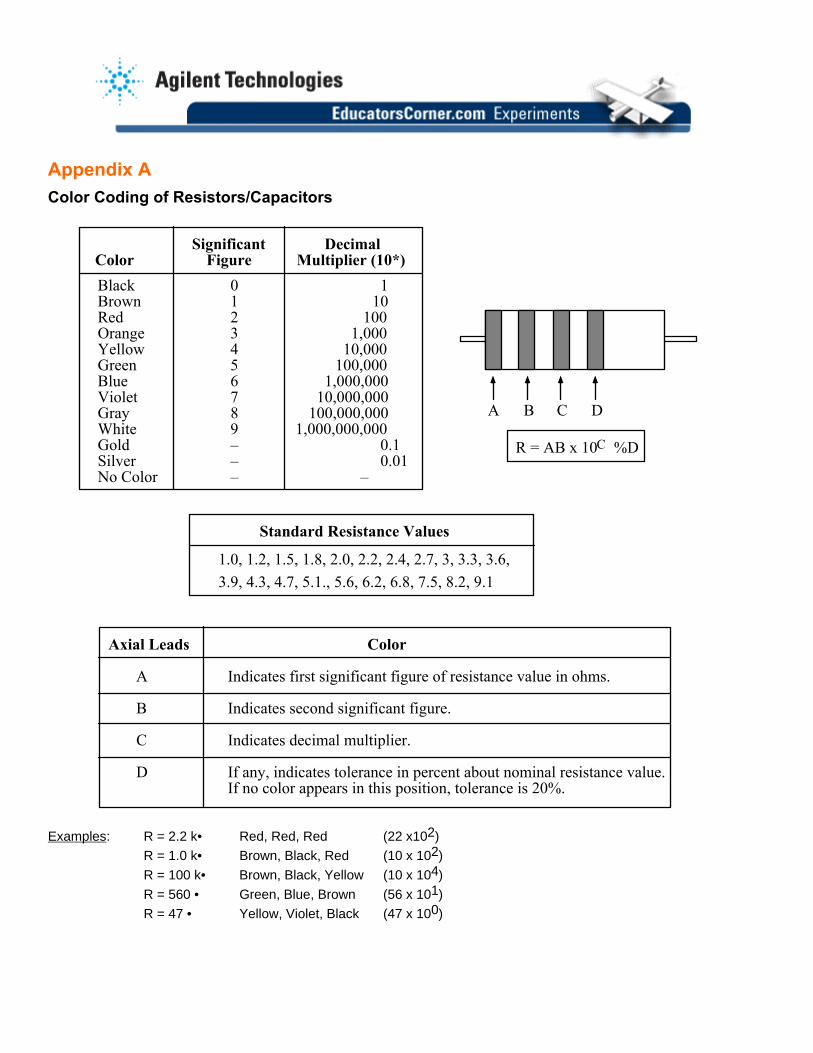
Appendix A Color Coding of Resistors/Capacitors
A B C D
R = AB x 10C %D
Standard Resistance Values
1.0, 1.2, 1.5, 1.8, 2.0, 2.2, 2.4, 2.7, 3, 3.3, 3.6,3.9, 4.3, 4.7, 5.1., 5.6, 6.2, 6.8, 7.5, 8.2, 9.1
Significant DecimalColor Figure Multiplier (10*)Black 0 1Brown 1 10Red 2 100Orange 3 1,000Yellow 4 10,000Green 5 100,000Blue 6 1,000,000Violet 7 10,000,000Gray 8 100,000,000White 9 1,000,000,000Gold – 0.1Silver – 0.01No Color – –
Axial Leads Color
A Indicates first significant figure of resistance value in ohms.
B Indicates second significant figure.
C Indicates decimal multiplier.
D If any, indicates tolerance in percent about nominal resistance value. If no color appears in this position, tolerance is 20%.
Examples: R = 2.2 k• Red, Red, Red (22 x102)
R = 1.0 k• Brown, Black, Red (10 x 102)
R = 100 k• Brown, Black, Yellow (10 x 104)
R = 560 • Green, Blue, Brown (56 x 101)
R = 47 • Yellow, Violet, Black (47 x 100)
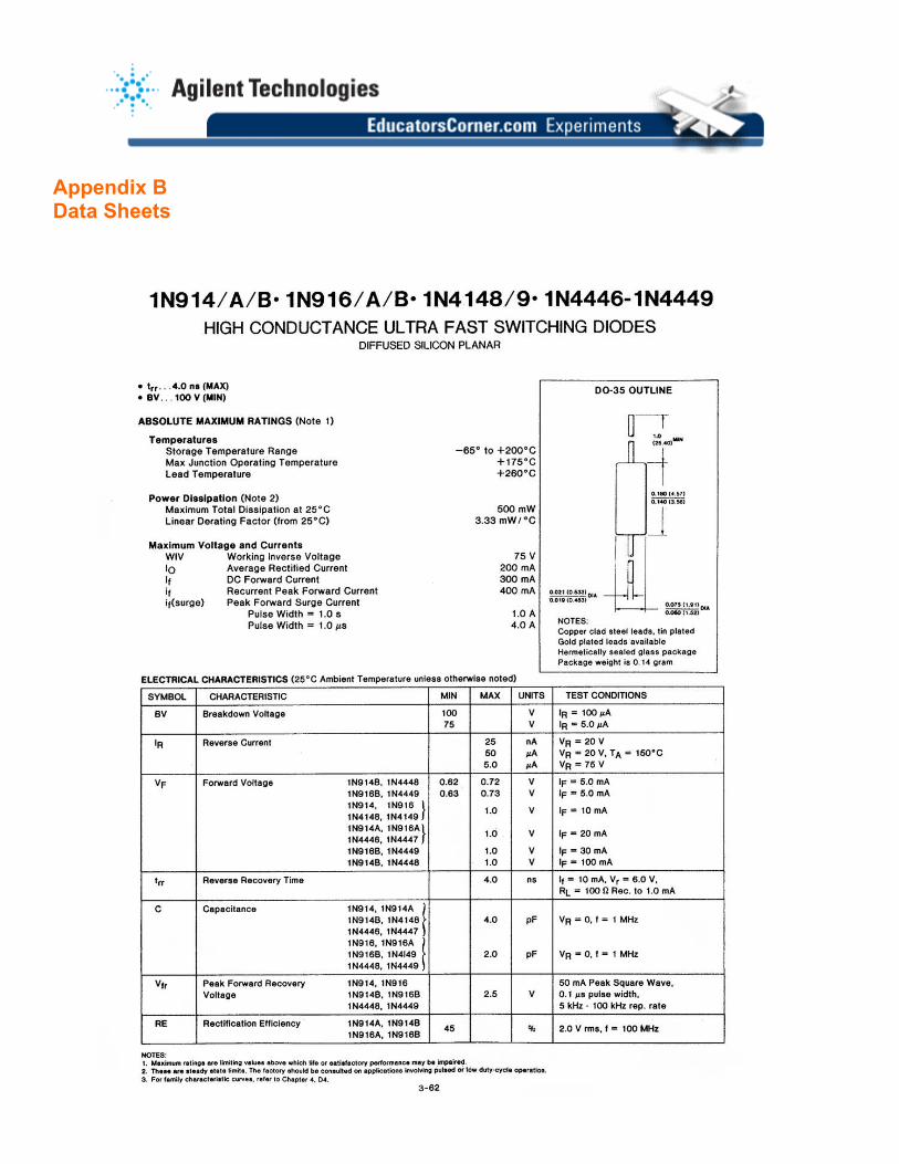
Appendix B Data Sheets