experiment 6 - we-online.com...experiment 6. the goal of this experiment is to analyze the impact of...
TRANSCRIPT
162 | TI-PMLK BUCK-WE Würth Elektronik
Experiment 6The goal of this experiment is to analyze the impact of the inductor on the closed
loop load-transient response of a peak-current mode controlled buck regulator.
The TPS54160 buck regulator is used for this experiment.
163 | TI-PMLK BUCK-WE Würth Elektronik
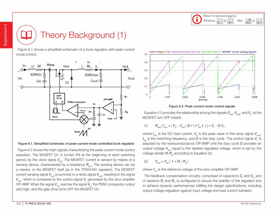
Figure 6.1 shows a simplified schematic of a buck regulator with peak-current mode control.
Figure 6.1. Simplified schematic of peak-current mode controlled buck regulator
Figure 6.2 shows the main signals characterizing the peak-current mode control operation. The MOSFET Q1 is turned ON at the beginning of each switching period, by the clock signal Vclk. The MOSFET current is sensed by means of a sensing device, characterized by a resistance Rsns. The sensing device can be a resistor, or the MOSFET itself (as in the TPS54160 regulator). The MOSFET current sensing signal Vsns is summed to a ramp signal Vrmp, resulting in the signal Vccr, which is compared to the control signal Vc generated by the error amplifier OP-AMP. When the signal Vccr reaches the signal Vc, the PWM comparator output sets high, and the gate drive turns OFF the MOSFET Q1.
Figure 6.2. Peak-current mode control signals
Equation (1) provides the relationship among the signals Vsns, Vrmp, and Vc, at the MOSFET turn OFF instant:
(1) Rsns [ Iout + ( Vin - Vout ) D / ( 2 fsw L ) ] = Vc - D Vp
where Iout is the DC load current, Vp is the peak value of the ramp signal Vrmp, fsw is the switching frequency, and D is the duty cycle. The control signal Vc is adjusted by the transconductance OP-AMP until the duty cycle D provides an output voltage Vout equal to the desired regulated voltage, which is set by the voltage divider Ri-Rg according to Equation (2):
(2) Vout = Vref ( 1 + Ri / Rg )
where Vref is the reference voltage of the error amplifier OP-AMP.
The feedback compensation circuitry, comprised of capacitors Cf and Co and of resistors Rf and Ri, is configured to ensure the stability of the regulator and to achieve dynamic performances fulfilling the design specifications, including output voltage regulation against input voltage and load current transient.
Exp
erim
ent
6
Theory Background (1)
+ +Windows: Mac:
Return to previous page by:

164 | TI-PMLK BUCK-WE Würth Elektronik
Equation (1) can be rewritten as shown in Equation (3):
(3) D = ( Vc - Rsns Iout ) / [ Vp + Rsns ( Vin - Vout ) / ( 2 fsw L ) ]
Equation (3) shows that, given the output voltage and load current, the duty cycle of a peak-current controlled buck regulator is instantly determined by the input voltage. If the input voltage increases, the duty cycle decreases, and viceversa. This is the well known feedforward feature characterizing the peak-current mode control, which makes such kind of control suitable for power supplies applications affected by large and fast input voltage variations, like in automotive power electronics. Equation (3) suggests that a higher value of the current sensing resistance Rsns improves the sensitivity of the duty cycle with respect to the input voltage.
The peak-current controlled buck regulator can be affected by a current-loop instability in operating conditions requiring a duty cycle greater than 0.5, that happens when the output voltage Vout is higher than half the input voltage Vin. The fixed ramp signal Vrmp helps preventing such instability. The stability is ensured at whatever duty cycle if the following constraint is fulfilled:
fixed ramp slope (4) r = ------------------------------------------------------------------ > 0.5 Rsns x inductor current slope in the OFF-ON state
Replacing the expressions of the fixed ramp and inductor current slope in the Equation (4) yields:
(5) r = Vp fsw L / ( Rsns Vout ) > 0.5
The value of the slope ratio r influences the transient response performance of the peak-current controlled buck regulator. A value of r closer to 0.5 involves better transient performance, but it increases the risk of instability caused by possible derating of the inductance L, connected to tolerance or determined by aging or saturation. A value of r much greater than 0.5 involves a degradation
of the inherent input voltage noise rejection capability of peak-current controlled buck regulator. A good setup range for the factor r is between 1 and 5.
Equations (3) and (5) highlight the manifold impact of the inductor on the peak-current controlled buck regulator. In particular, from (3) we see that a smaller inductance L increases the feedforward sensitivity of the peak-current mode control, whereas from (5) we see that a decrease of the inductance reduces the stability margin and requires higher Vp or lower Rsns. Moreover, according to (5), for a given inductance L, a lower switching frequency involves a decrease of the stability margin. Therefore, the condition (5) must be fulfilled in the worst case of minimum inductance and minimum switching frequency.
The closed loop transient performance of a peak-current mode controlled buck converter is determined by the voltage feedback compensation, implemented by means of the OP-AMP error amplifier. In particular, the voltage-loop gain of a peak-current controlled buck regulator is given by the simplified Equation (6):
Rout ( 1 + s / wz ) wo ( 1 + s / wz1 ) 1(6) T(s) = ---- ------------- ---- ---------------- ---- Rsns ( 1 + s / wp ) s ( 1 + s / wp1 ) Hs
where:
Rout = Vout / Iout wz = 1 / ( ESR Cout ) wp= 1 / ( Ro Cout )
wo= gmOTAH / Cf wz1= 1 / ( Rf Cf ) wp1= 1 / ( Rf Co )
Hs = 1 + s / ( Qs π fsw ) + s2 / ( π fsw )2 Qs = 1 / [ π ( 2 D’ - 0.5 ) ]
D' = 1- Vout / Vin H = Rg / ( Rg + Ri ) = Vref / Vout
The factor Hs accounts for the effects of the current sampling which characterizes the peak-current mode control. Equation (6) is valid at frequency much lower than the switching frequency fsw. In these conditions, if r is small, the current iL of the inductor is almost proportional to the control signal vc generated by the error amplifier, according to Equation (7):
(7) iL = vc / Rsns
Exp
erim
ent
6
Theory Background (2)
+ +Windows: Mac:
Return to previous page by:
165 | TI-PMLK BUCK-WE Würth Elektronik
Exp
erim
ent
6
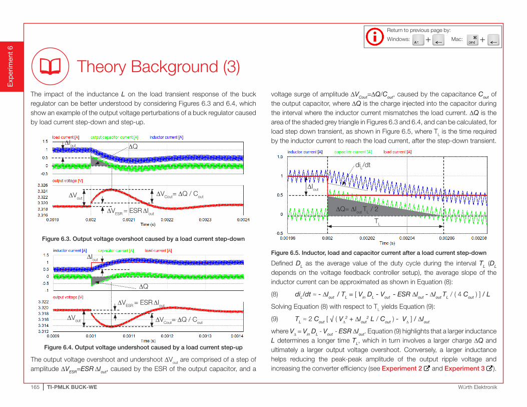
Theory Background (3)The impact of the inductance L on the load transient response of the buck regulator can be better understood by considering Figures 6.3 and 6.4, which show an example of the output voltage perturbations of a buck regulator caused by load current step-down and step-up.
DQ
DVoutDVCout= DQ / Cout
DVESR = ESR DIout
DIout
Figure 6.3. Output voltage overshoot caused by a load current step-down
DQ
DVout DVCout= DQ / Cout
DVESR = ESR DIout
DIout
Figure 6.4. Output voltage undershoot caused by a load current step-up
The output voltage overshoot and undershoot DVout are comprised of a step of amplitude DVESR=ESR DIout, caused by the ESR of the output capacitor, and a
voltage surge of amplitude DVCout=DQ/Cout, caused by the capacitance Cout of the output capacitor, where DQ is the charge injected into the capacitor during the interval where the inductor current mismatches the load current. DQ is the area of the shaded grey triangle in Figures 6.3 and 6.4, and can be calculated, for load step down transient, as shown in Figure 6.5, where TL is the time required by the inductor current to reach the load current, after the step-down transient.
diL/dt
DIout
TL
DQ= DIout TL / 2
Figure 6.5. Inductor, load and capacitor current after a load current step-down
Defined DL as the average value of the duty cycle during the interval TL (DL
depends on the voltage feedback controller setup), the average slope of the inductor current can be approximated as shown in Equation (8):
(8) diL/dt ≈ - DIout / TL = [ Vin DL - Vout - ESR DIout - DIout TL / ( 4 Cout ) ] / L
Solving Equation (8) with respect to TL yields Equation (9):
(9) TL ≈ 2 Cout [ √ ( VD2 + DIout
2 L / Cout ) - VD ] / DIout
where VD = Vin DL - Vout - ESR DIout. Equation (9) highlights that a larger inductance L determines a longer time TL, which in turn involves a larger charge DQ and ultimately a larger output voltage overshoot. Conversely, a larger inductance helps reducing the peak-peak amplitude of the output ripple voltage and increasing the converter efficiency (see Experiment 2 and Experiment 3 ).
+ +Windows: Mac:
Return to previous page by:
166 | TI-PMLK BUCK-WE Würth Elektronik
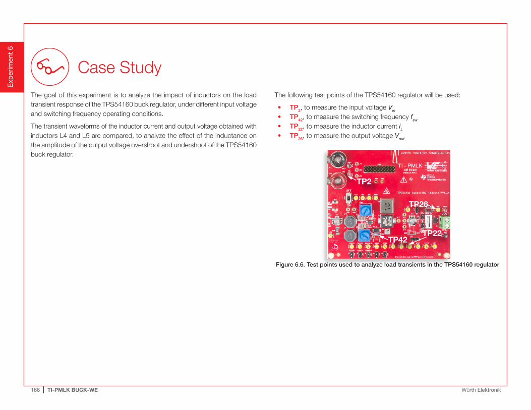
The goal of this experiment is to analyze the impact of inductors on the load transient response of the TPS54160 buck regulator, under different input voltage and switching frequency operating conditions.
The transient waveforms of the inductor current and output voltage obtained with inductors L4 and L5 are compared, to analyze the effect of the inductance on the amplitude of the output voltage overshoot and undershoot of the TPS54160 buck regulator.
The following test points of the TPS54160 regulator will be used:
• TP2, to measure the input voltage Vin
• TP42, to measure the switching frequency fsw
• TP22, to measure the inductor current iL• TP26, to measure the output voltage Vout
Figure 6.6. Test points used to analyze load transients in the TPS54160 regulator
Exp
erim
ent
6
Case Study
TP2
TP42
TP26
TP22
167 | TI-PMLK BUCK-WE Würth Elektronik
Experiment set-up: configuration
Exp
erim
ent
6
VO
LTA
GE
PR
OB
E 3
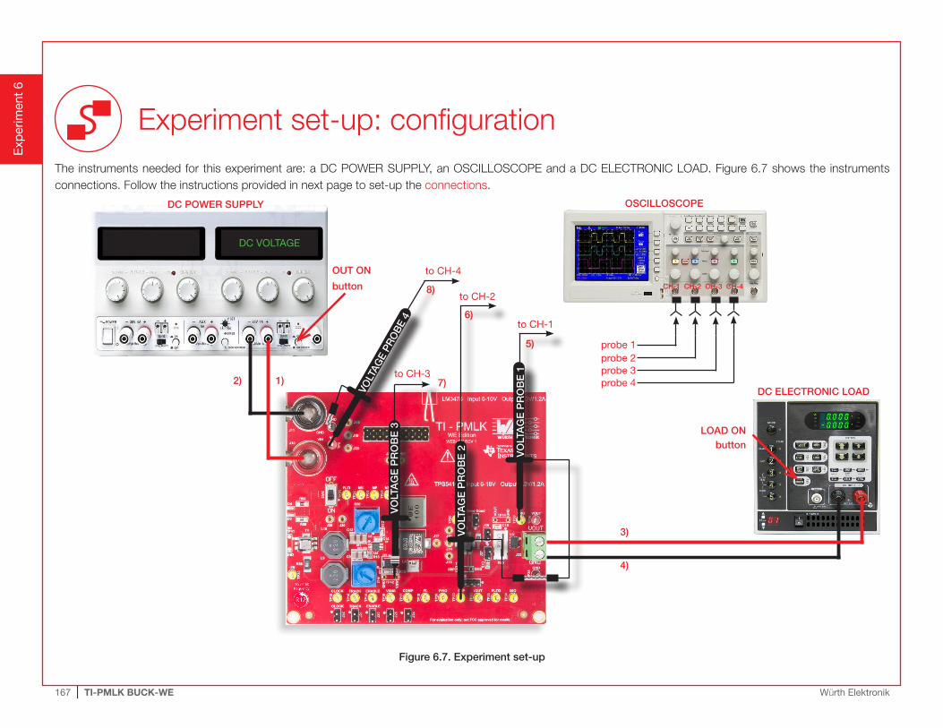
The instruments needed for this experiment are: a DC POWER SUPPLY, an OSCILLOSCOPE and a DC ELECTRONIC LOAD. Figure 6.7 shows the instruments connections. Follow the instructions provided in next page to set-up the connections.
Figure 6.7. Experiment set-up
DC POWER SUPPLY
DC VOLTAGE
OUT ON
button
to CH-31)
CH-1 CH-2 CH-3 CH-4
OSCILLOSCOPE
probe 1
2)
4)
7)
6)
5)
DC ELECTRONIC LOAD
LOAD ON button
to CH-2
to CH-1
probe 2probe 3
3)V
OLT
AG
E P
RO
BE
1
VO
LTA
GE
PR
OB
E 2
8)
to CH-4
VOLT
AGE
PRO
BE
4
probe 4
168 | TI-PMLK BUCK-WE Würth Elektronik
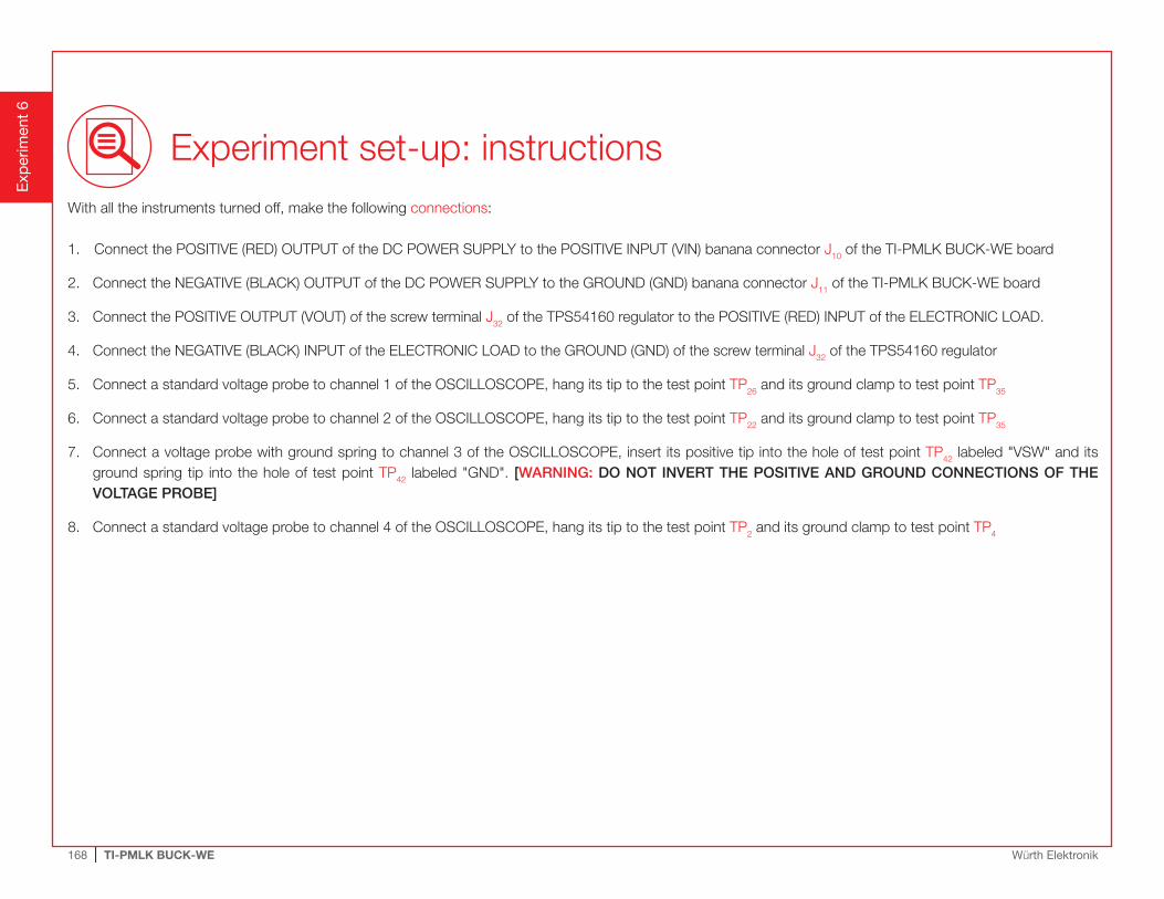
Experiment set-up: instructionsWith all the instruments turned off, make the following connections:
1. Connect the POSITIVE (RED) OUTPUT of the DC POWER SUPPLY to the POSITIVE INPUT (VIN) banana connector J10 of the TI-PMLK BUCK-WE board
2. Connect the NEGATIVE (BLACK) OUTPUT of the DC POWER SUPPLY to the GROUND (GND) banana connector J11 of the TI-PMLK BUCK-WE board
3. Connect the POSITIVE OUTPUT (VOUT) of the screw terminal J32 of the TPS54160 regulator to the POSITIVE (RED) INPUT of the ELECTRONIC LOAD.
4. Connect the NEGATIVE (BLACK) INPUT of the ELECTRONIC LOAD to the GROUND (GND) of the screw terminal J32 of the TPS54160 regulator
5. Connect a standard voltage probe to channel 1 of the OSCILLOSCOPE, hang its tip to the test point TP26 and its ground clamp to test point TP35
6. Connect a standard voltage probe to channel 2 of the OSCILLOSCOPE, hang its tip to the test point TP22 and its ground clamp to test point TP35
7. Connect a voltage probe with ground spring to channel 3 of the OSCILLOSCOPE, insert its positive tip into the hole of test point TP42 labeled "VSW" and itsground spring tip into the hole of test point TP42 labeled "GND". [WARNING: DO NOT INVERT THE POSITIVE AND GROUND CONNECTIONS OF THEVOLTAGE PROBE]
8. Connect a standard voltage probe to channel 4 of the OSCILLOSCOPE, hang its tip to the test point TP2 and its ground clamp to test point TP4
Exp
erim
ent
6
169 | TI-PMLK BUCK-WE Würth Elektronik
Test#1: instructions (1)
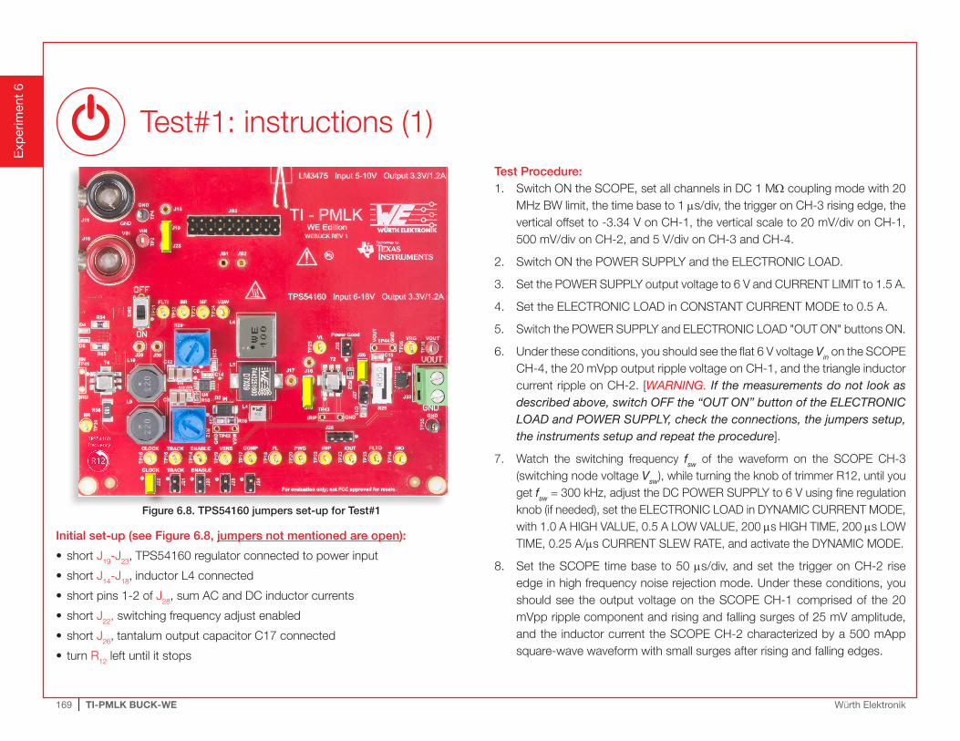
Figure 6.8. TPS54160 jumpers set-up for Test#1
Initial set-up (see Figure 6.8, jumpers not mentioned are open):
• short J19-J23, TPS54160 regulator connected to power input
• short J14-J18, inductor L4 connected
• short pins 1-2 of J28, sum AC and DC inductor currents
• short J22, switching frequency adjust enabled
• short J26, tantalum output capacitor C17 connected
• turn R12 left until it stops
Test Procedure:1. Switch ON the SCOPE, set all channels in DC 1 MW coupling mode with 20
MHz BW limit, the time base to 1 ms/div, the trigger on CH-3 rising edge, thevertical offset to -3.34 V on CH-1, the vertical scale to 20 mV/div on CH-1,500 mV/div on CH-2, and 5 V/div on CH-3 and CH-4.
2. Switch ON the POWER SUPPLY and the ELECTRONIC LOAD.
3. Set the POWER SUPPLY output voltage to 6 V and CURRENT LIMIT to 1.5 A.
4. Set the ELECTRONIC LOAD in CONSTANT CURRENT MODE to 0.5 A.
5. Switch the POWER SUPPLY and ELECTRONIC LOAD "OUT ON" buttons ON.
6. Under these conditions, you should see the flat 6 V voltage Vin on the SCOPECH-4, the 20 mVpp output ripple voltage on CH-1, and the triangle inductorcurrent ripple on CH-2. [WARNING. If the measurements do not look asdescribed above, switch OFF the “OUT ON” button of the ELECTRONICLOAD and POWER SUPPLY, check the connections, the jumpers setup,the instruments setup and repeat the procedure].
7. Watch the switching frequency fsw of the waveform on the SCOPE CH-3(switching node voltage Vsw), while turning the knob of trimmer R12, until youget fsw = 300 kHz, adjust the DC POWER SUPPLY to 6 V using fine regulationknob (if needed), set the ELECTRONIC LOAD in DYNAMIC CURRENT MODE,with 1.0 A HIGH VALUE, 0.5 A LOW VALUE, 200 ms HIGH TIME, 200 ms LOWTIME, 0.25 A/ms CURRENT SLEW RATE, and activate the DYNAMIC MODE.
8. Set the SCOPE time base to 50 ms/div, and set the trigger on CH-2 riseedge in high frequency noise rejection mode. Under these conditions, youshould see the output voltage on the SCOPE CH-1 comprised of the 20mVpp ripple component and rising and falling surges of 25 mV amplitude,and the inductor current the SCOPE CH-2 characterized by a 500 mAppsquare-wave waveform with small surges after rising and falling edges.
Exp
erim
ent
6
3 2 1
170 | TI-PMLK BUCK-WE Würth Elektronik
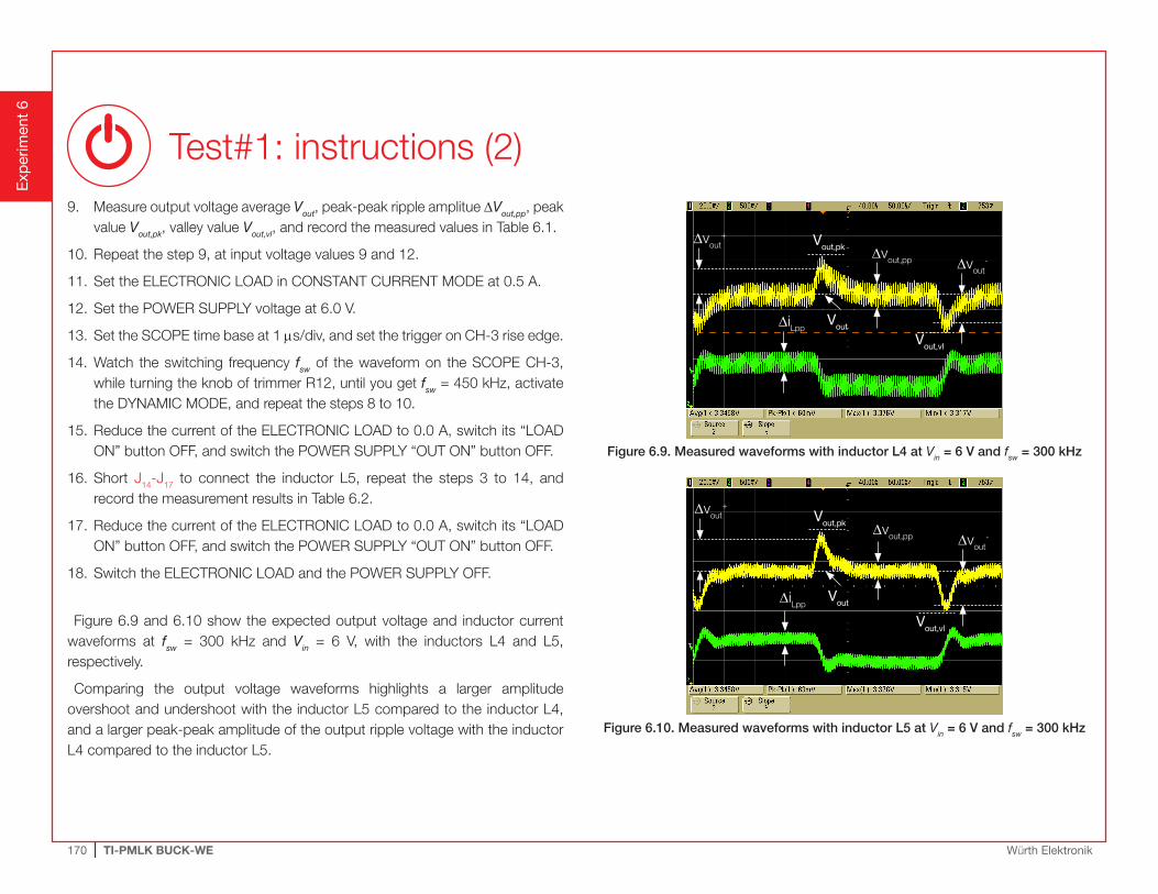
9. Measure output voltage average Vout, peak-peak ripple amplitue DVout,pp, peakvalue Vout,pk, valley value Vout,vl, and record the measured values in Table 6.1.
10. Repeat the step 9, at input voltage values 9 and 12.
11. Set the ELECTRONIC LOAD in CONSTANT CURRENT MODE at 0.5 A.
12. Set the POWER SUPPLY voltage at 6.0 V.
13. Set the SCOPE time base at 1 ms/div, and set the trigger on CH-3 rise edge.
14. Watch the switching frequency fsw of the waveform on the SCOPE CH-3,while turning the knob of trimmer R12, until you get fsw = 450 kHz, activatethe DYNAMIC MODE, and repeat the steps 8 to 10.
15. Reduce the current of the ELECTRONIC LOAD to 0.0 A, switch its “LOADON” button OFF, and switch the POWER SUPPLY “OUT ON” button OFF.
16. Short J14-J17 to connect the inductor L5, repeat the steps 3 to 14, andrecord the measurement results in Table 6.2.
17. Reduce the current of the ELECTRONIC LOAD to 0.0 A, switch its “LOADON” button OFF, and switch the POWER SUPPLY “OUT ON” button OFF.
18. Switch the ELECTRONIC LOAD and the POWER SUPPLY OFF.
Figure 6.9 and 6.10 show the expected output voltage and inductor current waveforms at fsw = 300 kHz and Vin = 6 V, with the inductors L4 and L5, respectively.
Comparing the output voltage waveforms highlights a larger amplitude overshoot and undershoot with the inductor L5 compared to the inductor L4, and a larger peak-peak amplitude of the output ripple voltage with the inductor L4 compared to the inductor L5.
Vout
Dvout+
Dvout-
Dvout,pp
DiLpp
Vout,pk
Vout,vl
Figure 6.9. Measured waveforms with inductor L4 at Vin = 6 V and fsw = 300 kHz
Vout
Dvout+
Dvout-
Dvout,pp
DiLpp
Vout,pk
Vout,vl
Figure 6.10. Measured waveforms with inductor L5 at Vin = 6 V and fsw = 300 kHz
Test#1: instructions (2)
Exp
erim
ent
6
171 | TI-PMLK BUCK-WE Würth Elektronik
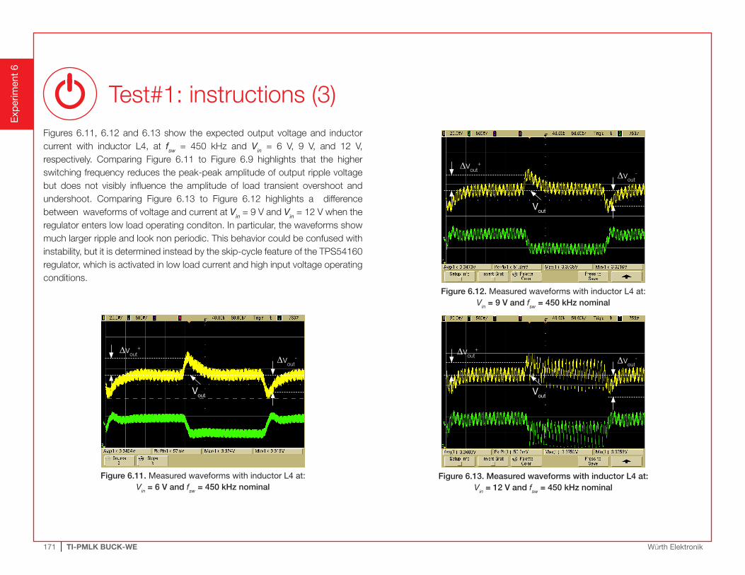
Figures 6.11, 6.12 and 6.13 show the expected output voltage and inductor current with inductor L4, at fsw = 450 kHz and Vin = 6 V, 9 V, and 12 V, respectively. Comparing Figure 6.11 to Figure 6.9 highlights that the higher switching frequency reduces the peak-peak amplitude of output ripple voltage but does not visibly influence the amplitude of load transient overshoot and undershoot. Comparing Figure 6.13 to Figure 6.12 highlights a difference between waveforms of voltage and current at Vin = 9 V and Vin = 12 V when the regulator enters low load operating conditon. In particular, the waveforms show much larger ripple and look non periodic. This behavior could be confused with instability, but it is determined instead by the skip-cycle feature of the TPS54160 regulator, which is activated in low load current and high input voltage operating conditions.
Vout
Dvout+
Dvout-
Figure 6.11. Measured waveforms with inductor L4 at:Vin = 6 V and fsw = 450 kHz nominal
Vout
Dvout+
Dvout-
Figure 6.12. Measured waveforms with inductor L4 at:Vin = 9 V and fsw = 450 kHz nominal
Vout
Dvout+
Dvout-
Figure 6.13. Measured waveforms with inductor L4 at:Vin = 12 V and fsw = 450 kHz nominal
Test#1: instructions (3)
Exp
erim
ent
6
172 | TI-PMLK BUCK-WE Würth Elektronik
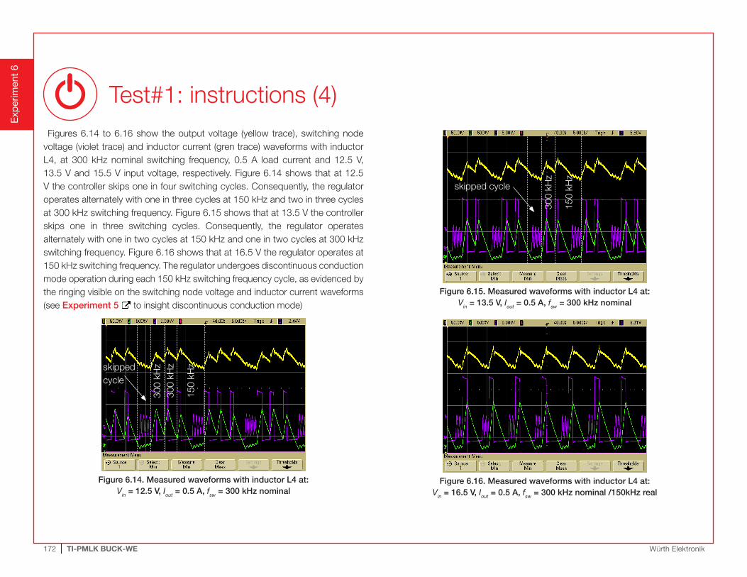
Figures 6.14 to 6.16 show the output voltage (yellow trace), switching node voltage (violet trace) and inductor current (gren trace) waveforms with inductor L4, at 300 kHz nominal switching frequency, 0.5 A load current and 12.5 V, 13.5 V and 15.5 V input voltage, respectively. Figure 6.14 shows that at 12.5 V the controller skips one in four switching cycles. Consequently, the regulator operates alternately with one in three cycles at 150 kHz and two in three cycles at 300 kHz switching frequency. Figure 6.15 shows that at 13.5 V the controller skips one in three switching cycles. Consequently, the regulator operates alternately with one in two cycles at 150 kHz and one in two cycles at 300 kHz switching frequency. Figure 6.16 shows that at 16.5 V the regulator operates at 150 kHz switching frequency. The regulator undergoes discontinuous conduction mode operation during each 150 kHz switching frequency cycle, as evidenced by the ringing visible on the switching node voltage and inductor current waveforms (see Experiment 5 to insight discontinuous conduction mode)
skippedcycle
300
kHz
300
kHz
150
kHz
Figure 6.14. Measured waveforms with inductor L4 at:Vin = 12.5 V, Iout = 0.5 A, fsw = 300 kHz nominal
skipped cycle
300
kHz
150
kHz
Figure 6.15. Measured waveforms with inductor L4 at:Vin = 13.5 V, Iout = 0.5 A, fsw = 300 kHz nominal
Figure 6.16. Measured waveforms with inductor L4 at:Vin = 16.5 V, Iout = 0.5 A, fsw = 300 kHz nominal /150kHz real
Test#1: instructions (4)
Exp
erim
ent
6
173 | TI-PMLK BUCK-WE Würth Elektronik
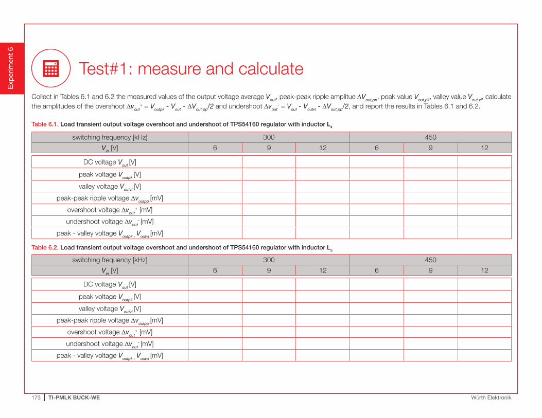
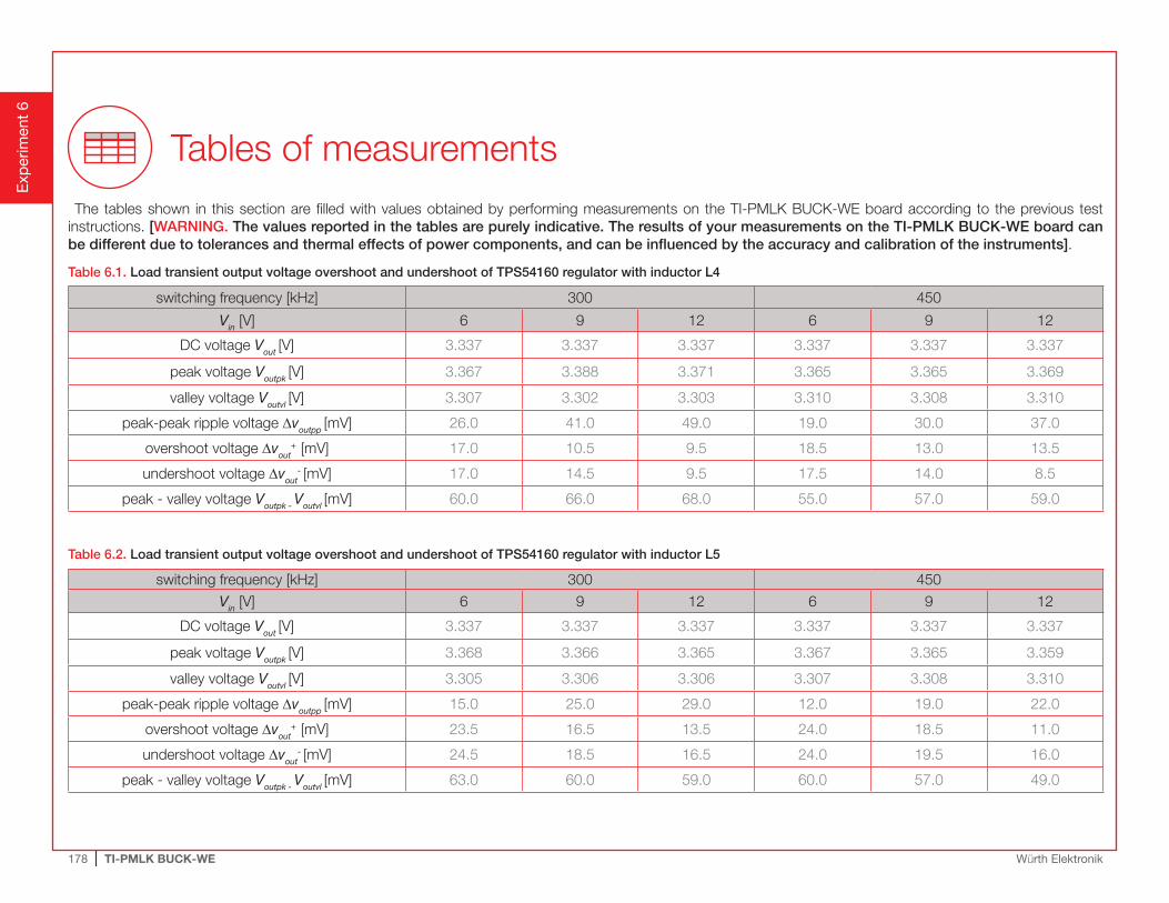
Test#1: measure and calculateCollect in Tables 6.1 and 6.2 the measured values of the output voltage average Vout, peak-peak ripple amplitue DVout,pp, peak value Vout,pk, valley value Vout,vl, calculate the amplitudes of the overshoot Dvout
+ = Voutpk - Vout - DVout,pp/2 and undershoot Dvout- = Vout - Voutvl - DVout,pp/2, and report the results in Tables 6.1 and 6.2.
Table 6.1. Load transient output voltage overshoot and undershoot of TPS54160 regulator with inductor L4
switching frequency [kHz] 300 450
Vin [V] 6 9 12 6 9 12
DC voltage Vout [V]
peak voltage Voutpk [V]
valley voltage Voutvl [V]
peak-peak ripple voltage Dvoutpp [mV]
overshoot voltage Dvout+
[mV]
undershoot voltage Dvout- [mV]
peak - valley voltage Voutpk - Voutvl [mV]
Table 6.2. Load transient output voltage overshoot and undershoot of TPS54160 regulator with inductor L5
switching frequency [kHz] 300 450
Vin [V] 6 9 12 6 9 12
DC voltage Vout [V]
peak voltage Voutpk [V]
valley voltage Voutvl [V]
peak-peak ripple voltage Dvoutpp [mV]
overshoot voltage Dvout+
[mV]
undershoot voltage Dvout- [mV]
peak - valley voltage Voutpk - Voutvl [mV]
Exp
erim
ent
6

174 | TI-PMLK BUCK-WE Würth Elektronik
1 Which inductor does determine the largest load transient overshoot and undershoot?
L4 L5 no difference it depends on the input voltage it depends on the switching frequency other: ________________________
Please comment your answer: ________________________________________________________________________________________________________________
____________________________________________________________________________________________________________________________________________
2 How does the input voltage influence the amplitude of load transient overshoot and undershoot?
no influence larger overshoot/undershoot at higher voltage larger overshoot/undershoot at lower voltage other: ________________________
Please comment your answer: ________________________________________________________________________________________________________________
____________________________________________________________________________________________________________________________________________
3 How does the switching frequency influence the amplitude of load transient overshoot and undershoot?
no influence larger overshoot/undershoot at higher frequency larger overshoot/undershoot at lower frequency other: ________________________
Please comment your answer: __________________________________________________________________________________________________________________
____________________________________________________________________________________________________________________________________________
4 Which inductor does determine the largest load transient peak voltage to valley voltage amplitude?
L4 L5 no difference it depends on the input voltage it depends on the switching frequency other: ________________________
Please comment your answer: ________________________________________________________________________________________________________________
____________________________________________________________________________________________________________________________________________
Exp
erim
ent
6
Observe and Answer?
175 | TI-PMLK BUCK-WE Würth Elektronik
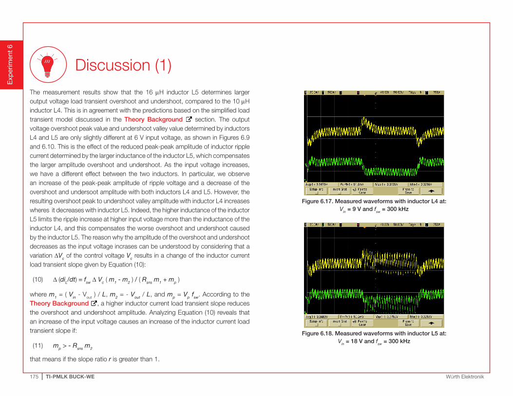
Discussion (1)The measurement results show that the 16 mH inductor L5 determines larger output voltage load transient overshoot and undershoot, compared to the 10 mH inductor L4. This is in agreement with the predictions based on the simplified load transient model discussed in the Theory Background section. The output voltage overshoot peak value and undershoot valley value determined by inductors L4 and L5 are only slightly different at 6 V input voltage, as shown in Figures 6.9 and 6.10. This is the effect of the reduced peak-peak amplitude of inductor ripple current determined by the larger inductance of the inductor L5, which compensates the larger amplitude overshoot and undershoot. As the input voltage increases, we have a different effect between the two inductors. In particular, we observe an increase of the peak-peak amplitude of ripple voltage and a decrease of the overshoot and undersoot amplitude with both inductors L4 and L5. However, the resulting overshoot peak to undershoot valley amplitude with inductor L4 increases wheres it decreases with inductor L5. Indeed, the higher inductance of the inductor L5 limits the ripple increase at higher input voltage more than the inductance of the inductor L4, and this compensates the worse overshoot and undershoot caused by the inductor L5. The reason why the amplitude of the overshoot and undershoot decreases as the input voltage incrases can be understood by considering that a variation DVc of the control voltage Vc results in a change of the inductor current load transient slope given by Equation (10):
(10) D (diL/dt) = fsw D Vc ( m1 - m2 ) / ( Rsns m1 + mp )
where m1 = ( Vin - Vout ) / L, m2 = - Vout / L, and mp = Vp fsw. According to the Theory Background , a higher inductor current load transient slope reduces the overshoot and undershoot amplitude. Analyzing Equation (10) reveals that an increase of the input voltage causes an increase of the inductor current load transient slope if:
(11) mp > - Rsns m2
that means if the slope ratio r is greater than 1.
Figure 6.17. Measured waveforms with inductor L4 at:Vin = 9 V and fsw = 300 kHz
Figure 6.18. Measured waveforms with inductor L5 at:Vin = 18 V and fsw = 300 kHz
Exp
erim
ent
6
176 | TI-PMLK BUCK-WE Würth Elektronik
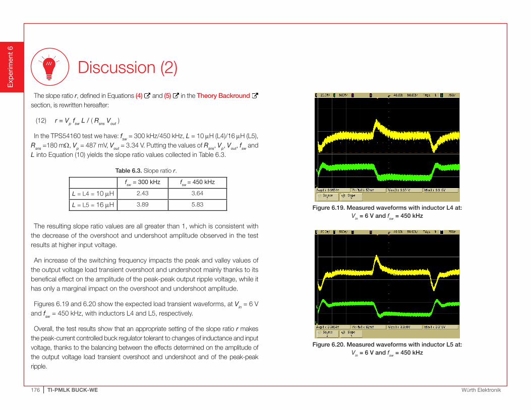
Discussion (2)
The slope ratio r, defined in Equations (4) and (5) in the Theory Backround section, is rewritten hereafter:
(12) r = Vp fsw L / ( Rsns Vout )
In the TPS54160 test we have: fsw = 300 kHz/450 kHz, L = 10 mH (L4)/16 mH (L5), Rsns =180 mW, Vp = 487 mV, Vout = 3.34 V. Putting the values of Rsns, Vp, Vout, fsw and L into Equation (10) yields the slope ratio values collected in Table 6.3.
Table 6.3. Slope ratio r.
fsw = 300 kHz fsw = 450 kHz
L = L4 = 10 mH 2.43 3.64
L = L5 = 16 mH 3.89 5.83
The resulting slope ratio values are all greater than 1, which is consistent with the decrease of the overshoot and undershoot amplitude observed in the test results at higher input voltage.
An increase of the switching frequency impacts the peak and valley values of the output voltage load transient overshoot and undershoot mainly thanks to its benefical effect on the amplitude of the peak-peak output ripple voltage, while it has only a marginal impact on the overshoot and undershoot amplitude.
Figures 6.19 and 6.20 show the expected load transient waveforms, at Vin = 6 V and fsw = 450 kHz, with inductors L4 and L5, respectively.
Overall, the test results show that an appropriate setting of the slope ratio r makes the peak-current controlled buck regulator tolerant to changes of inductance and input voltage, thanks to the balancing between the effects determined on the amplitude of the output voltage load transient overshoot and undershoot and of the peak-peak ripple.
Figure 6.19. Measured waveforms with inductor L4 at:Vin = 6 V and fsw = 450 kHz
Figure 6.20. Measured waveforms with inductor L5 at:Vin = 6 V and fsw = 450 kHz
Exp
erim
ent
6

177 | TI-PMLK BUCK-WE Würth Elektronik
Expansion Activities
Exp
erim
ent
6
• Repeat the experiment with different amplitude of load current step.
178 | TI-PMLK BUCK-WE Würth Elektronik
Exp
erim
ent
6
The tables shown in this section are filled with values obtained by performing measurements on the TI-PMLK BUCK-WE board according to the previous test instructions. [WARNING. The values reported in the tables are purely indicative. The results of your measurements on the TI-PMLK BUCK-WE board can be different due to tolerances and thermal effects of power components, and can be influenced by the accuracy and calibration of the instruments].
Table 6.1. Load transient output voltage overshoot and undershoot of TPS54160 regulator with inductor L4
switching frequency [kHz] 300 450
Vin [V] 6 9 12 6 9 12
DC voltage Vout [V] 3.337 3.337 3.337 3.337 3.337 3.337
peak voltage Voutpk [V] 3.367 3.388 3.371 3.365 3.365 3.369
valley voltage Voutvl [V] 3.307 3.302 3.303 3.310 3.308 3.310
peak-peak ripple voltage Dvoutpp [mV] 26.0 41.0 49.0 19.0 30.0 37.0
overshoot voltage Dvout+
[mV] 17.0 10.5 9.5 18.5 13.0 13.5
undershoot voltage Dvout- [mV] 17.0 14.5 9.5 17.5 14.0 8.5
peak - valley voltage Voutpk - Voutvl [mV] 60.0 66.0 68.0 55.0 57.0 59.0
Table 6.2. Load transient output voltage overshoot and undershoot of TPS54160 regulator with inductor L5
switching frequency [kHz] 300 450
Vin [V] 6 9 12 6 9 12
DC voltage Vout [V] 3.337 3.337 3.337 3.337 3.337 3.337
peak voltage Voutpk [V] 3.368 3.366 3.365 3.367 3.365 3.359
valley voltage Voutvl [V] 3.305 3.306 3.306 3.307 3.308 3.310
peak-peak ripple voltage Dvoutpp [mV] 15.0 25.0 29.0 12.0 19.0 22.0
overshoot voltage Dvout+
[mV] 23.5 16.5 13.5 24.0 18.5 11.0
undershoot voltage Dvout- [mV] 24.5 18.5 16.5 24.0 19.5 16.0
peak - valley voltage Voutpk - Voutvl [mV] 63.0 60.0 59.0 60.0 57.0 49.0
Tables of measurements