experimental characterization of the 192 channel clear-pem
TRANSCRIPT
ARTICLE IN PRESS
Nuclear Instruments and Methods in Physics Research A 598 (2009) 802–814
Contents lists available at ScienceDirect
Nuclear Instruments and Methods inPhysics Research A
0168-90
doi:10.1
� Corr
E-m
journal homepage: www.elsevier.com/locate/nima
Experimental characterization of the 192 channel Clear-PEM frontend ASICcoupled to a multi-pixel APD readout of LYSO:Ce crystals
Edgar Albuquerque a, Vasco Bexiga a, Ricardo Bugalho b, Bruno Carric-o b, Claudia S. Ferreira b,Miguel Ferreira b, Joaquim Godinho c, Fernando Gonc-alves a, Carlos Leong a, Pedro Lousa c,Pedro Machado a, Rui Moura b, Pedro Neves c, Catarina Ortigao b, Fernando Piedade c, Joao F. Pinheiro b,Joel Rego c, Angelo Rivetti d, Pedro Rodrigues b,�, Jose C. Silva b, Manuel M. Silva a, Isabel C. Teixeira a,e,Joao P. Teixeira a,e, Andreia Trindade b, Joao Varela b,e,f
a INESC-ID, Rua Alves Redol 9, 1000-129 Lisboa, Portugalb LIP, Avenida Elias Garcia 14-1, 1000-149 Lisboa, Portugalc INOV, Rua Alves Redol 9, 1000-129 Lisboa, Portugald INFN, Torino, Italye IST, Avenida Rovisco Pais, 1049-001 Lisboa, Portugalf CERN, Route Meyrin, 1211 Geneva, Switzerland
a r t i c l e i n f o
Article history:
Received 23 July 2008
Received in revised form
23 September 2008
Accepted 1 October 2008Available online 17 October 2008
Keywords:
PET
Avalanche photodiodes
ASIC
Frontend electronics
02/$ - see front matter & 2007 Elsevier B.V. A
016/j.nima.2008.10.005
esponding author. Tel.: +351 21797 38 80; fax
ail address: [email protected] (P. Rodrigues).
a b s t r a c t
In the framework of the Clear-PEM project for the construction of a high-resolution scanner for breast
cancer imaging, a very compact and dense frontend electronics system has been developed for readout
of multi-pixel S8550 Hamamatsu APDs. The frontend electronics are instrumented with a mixed-signal
Application-Specific Integrated Circuit (ASIC), which incorporates 192 low-noise charge pre-amplifiers,
shapers, analog memory cells and digital control blocks. Pulses are continuously stored in memory cells
at clock frequency. Channels above a common threshold voltage are readout for digitization by off-chip
free-sampling ADCs. The ASIC has a size of 7:3� 9:8 mm2 and was implemented in a AMS 0:35mm
CMOS technology. In this paper the experimental characterization of the Clear-PEM frontend ASIC,
reading out multi-pixel APDs coupled to LYSO:Ce crystal matrices, is presented. The chips were
mounted on a custom test board connected to six APD arrays and to the data acquisition system. Six 32-
pixel LYSO:Ce crystal matrices coupled on both sides to APD arrays were readout by two test boards. All
384 channels were operational. The chip power consumption is 660 mW (3.4 mW per channel). A very
stable behavior of the chip was observed, with an estimated ENC of 120021300e� at APD gain 100. The
inter-channel noise dispersion and mean baseline variation is less than 8% and 0.5%, respectively. The
spread in the gain between different channels is found to be 1.5%. Energy resolution of 16.5% at 511 keV
and 12.8% at 662 keV has been measured. Timing measurements between the two APDs that readout
the same crystal is extracted and compared with detailed Monte Carlo simulations. At 511 keV
the measured single photon time RMS resolution is 1.30 ns, in very good agreement with the expected
value of 1.34 ns.
& 2007 Elsevier B.V. All rights reserved.
1. Introduction
Nowadays, PET is recognized as a powerful imaging techniquefor the detection of tumors in oncological diseases. 18F-FDG PETimaging allows to map areas of localized increase of metabolicactivity that may indicate the presence of a neoplasm beforemorphological changes are detected by other imaging modalities.This is the example of breast cancer where PET is more efficient to
ll rights reserved.
: +35121793 46 31.
detect lesions and to distinguish benign findings from malignformations in comparison with standard mammography techni-ques (X-ray). 18F-FDG PET for the evaluation of breast cancer hasstarted in 1989, resulting in a published study on 17 breast cancerpatients in advanced stage [1]. Subsequent analysis of combinedclinical trials with 259 patients has yield a sensitivity (truepositive/total positive) of 92% and specificity (true negative/totalnegative) of 94%. Almost all exams were carried out with a whole-body PET scanner, which may justify that although sensitivity wasabout 90% for tumors larger than 2 cm [2] it decreases to 25%when lesions with diameters less than 1 cm are considered. Thedecrease in small breast tumors detectability performance is

ARTICLE IN PRESS
E. Albuquerque et al. / Nuclear Instruments and Methods in Physics Research A 598 (2009) 802–814 803
mostly due to the suboptimal spatial resolution of current whole-body PET scanners [3]. Spatial resolution in whole-body PET islimited to 0.5–1 cm which has prevented the use of PET imagingexclusively for breast cancer screening purposes [4].
At the light of the current limitations of whole-body PETscanners for breast cancer detection and motivated by the factthat PET facilities have a low patient turnover and high cost formass screening, in terms of the required equipment andpersonnel, dedicated specially tailored PET systems have beenadvocated [3,5,6]. Such devices, generally named Positron Emis-sion Mammography (PEM), are designed to image the breastregion by favoring high-resolution and detection sensitivity overthe general purpose of whole-body scanners. The design goals forPEM instruments include short imaging time, high spatialresolution, improved diagnostic specificity to reduce the needfor surgical biopsies and confident definition of tumor prior tobiopsy or other surgical options.
The geometry of a dedicated PET scanner for mammographyshould provide a large angular coverage by placing the detectorsas close as possible to the breast. The photodetector elementsshould be based on high-Z stopping power materials, with anadequate thickness and an enhanced photoelectric interactionprobability, while the readout electronics should not contribute todegradation on the spatial resolution. When planar detectors arelocated close to the object under examination, the thickness of thephoton detection sensitive material may introduce deteriorationon the spatial resolution due to the so-called parallax effect. Thiseffect originates from the fact that conventional PET scanners arenot capable of determining the position of the photon interactionalong the detection material.
The parallax error becomes more severe as the distancebetween the opposing detection elements decreases, or theangular range of accepted events increases [6,7]. Therefore, it isdesirable that the readout method should be compatible with theestimation of the depth-of-interaction (DOI) along the crystallongitudinal dimension. In addition, and since the large fraction ofthe injected dose would be located outside the field-of-view(FOV), namely in the heart, liver and torso, the detector shouldhave a low deadtime at channel level and a good timemeasurement capability to minimize the accidental coincidencesdue to the single photon background rate. An efficient dataacquisition system, capable of on-line single event rejection with aminimum processing deadtime is required, lowering the datarates to a level compatible with general purpose high-speed datalinks and off-the-shell mass storage systems.
The Clear-PEM scanner has being developed by the PortuguesePET Consortium under the framework of the Crystal ClearCollaboration [8–10]. The major technical specifications arepresented in Table 1. The detector assembly is based on two
Table 1Clear-PEM scanner main technical specifications.
Parameter Value
Number of LYSO:Ce crystals 6144 (2� 2� 20 mm3 each)
Number of crystal matrices 192
Number of electronic channels 12 288
Number of multi-pixel APDs 384
Number of multi-channel ASICs 64
Frontend to L1 bandwidth 78 (50 MHz) up to 156 Gbps (100 MHz)
L1–L2 bandwidth 400 (50 MHz)–800 MB/s (100 MHz)
Number of LORs 37 748 736
Scintillator volume 491:52 cm3 ð� 3:5 kgÞ
Active surface area 17� 15 cm2 ð� 13 channels=cm2Þ
Separation distance 5–40 cm
Osolid angle at 10 cm separation 0.47
detecting planar heads, with a 17� 15 cm2 FOV [9]. The detectionheads are mounted on a robotized mechanical system, enablingthe exam of both breasts, one at a time, as well as the axillarylymph nodes. The Clear-PEM scanner adopts LuxY2�xSiO5
(LYSO:Ce) [11] scintillator crystals with individual dimensions of2� 2� 20 mm3. The traditional readout based on photomulti-pliers is replaced by multi-pixel avalanche photodiodes (APD).Due to its compactness, it is possible to read each single crystalwith one APD pixel on each ends, and to use the relativeamplitude of the two signals to estimate the longitudinalcoordinate of the interaction point [12,13]. This solution named‘‘double readout’’ cannot be easily implemented in conventionalwhole-body ring or planar PET scanners, since the amount of non-active material (electronics and photomultipliers) placed betweenthe anatomic region under examination and the crystals wouldlead to an unacceptable decrease of the detection efficiency due tothe reduction of the solid angular coverage and additionalattenuation of the incoming photons.
The individual 1:1 crystal-pixel APD coupling scheme leads to12 288 channels, with a density at about 13 channels percentimeter square. The limited available space in the patient portto place the cooling equipment, required in face of the influence oftemperature on the APD performance (�2:5% K at gain M ¼ 50 andincrease of dark current by a factor of 2 per 11 K) demand that allthe processing electronics must have a strict limited powerconsumption and thermal dissipation budget. This and the lowgain (50–200) of the APDs has lead to the development, for theClear-PEM scanner, of a family of specifically tailored low-noiseVLSI chips. The output pulses are digitized by free-sampling ADCs.The most demanding data processing task is concentrated in theoff-detector electronics, based on a reconfigurable FPGA fabric[10], which implements a first-trigger (L1) decision. The onlinetrigger extract the pulse features (energy and time) needed for atwo-photon coincidence decision, discarding out-of-time singlephotons. The data rate to be stored in mass storage elements canreach up to 250 MByte/s [14,15]. Accepted events are revalidatedby a second trigger (L2), software based on a multi-core server,that re-process the datastream with more complex algorithms forthe determination of energy, time, DOI and assignment of thecrystal of first interaction, for events with multiple hits due to in-detector Compton. Second-level accepted triggers are then storedand used as input for the image reconstruction algorithms.
2. The Clear-PEM frontend electronics
The Frontend Electronics System, physically located on thedetector heads, performs signal amplification, channel selectionand analog multiplexing, analog to digital conversion and parallel-to-serial translation. The frontend electronics block is, in severalaspects, one of the most sensitive and critical sub-system of theClear-PEM detector. The frontend chip must be low-noise, due tothe initial reduced charge at the amplifier input, which for a511 keV photon energy deposit is around 30 fC (maximum value),or a peak current around 0.75 nA, assuming a LYSO:Ce 42 ns timeconstant [11]. The frontend chip should amplify this charge byabout three orders of magnitude, while complying with the low-power dissipation requirements, compatible with a compactcooling system. A cooling system is required since the LYSO:Celight yield and APD gain are inversely dependent on thetemperature. The collected charge at the input is constrained bythe S8550 APD gain, crystal-APD pixel size mismatch, and to thefact that in each crystal the light is split by two photosensors.Since the Frontend Boards (FEBs), in which the Application-Specific Integrated Circuits (ASICs) are mounted, have a mixedanalog–digital environment, special care is needed regarding the

ARTICLE IN PRESS
E. Albuquerque et al. / Nuclear Instruments and Methods in Physics Research A 598 (2009) 802–814804
correct conditioning of the digital, large amplitude, high-frequency signals from clocks and other periodic signals. Noisepickup in the PCB traces that connect the APD outputs to thefrontend chips must also be minimized by keeping the tracelength as small as possible of about a few millimeters.
The Clear-PEM ASIC is designed for the readout of HamamatsuS8550 multi-pixel APD. Specifications for this APD are summar-ized in Table 2 and in Refs. [16–18]. The noise specification of theASIC amplifiers is a function of the energy and time resolutionrequirements. An equivalent noise charge (ENC) of around100021500e� RMS contributes less than 2% to the energyresolution, which at 511 keV is dominated by the LYSO:Ce intrinsicand photostatistics terms to the energy resolution [19]. For asignal peaking time of 30-40 ns, this noise level implies a RMStime resolution of the order of 1 ns. To achieve peaking times ofthis order, a fast amplifier response (15–20 ns) is required, roughlyhalf of the LYSO:Ce decay time. In this circumstances only 40–50%of the input charge contributes to the amplitude of the outputpulse. In overall, a gain of 30–40 mV/fC (defined here as the gain ofthe output pulse in response to a Dirac-like charge input) isrequired. Power and cabling constrains required that some form ofmultiplexing and zero suppression should be implemented in thechip, keeping to a minimum the number of output channels. Thenumber of output channels in a scanner based on crystals withsmall cross-section has to be chosen adequately in order to avoidsignificant losses of information that could compromise thedetection sensitivity of two-photon events in coincidence. MonteCarlo results show that in the case of Clear-PEM about 53% of allcoincidences will have two or more crystal hits in a given detectorhead per event [9]. Therefore, the number of output channels forthe frontend ASIC should be 2, still allowing for the readout of
Table 2Hamamatsu S8550 APD electrical and optical characteristics.
Parameter Value
Pixel size 1:6 mm� 1:6 mm (�32 pixels)
Pixel pitch 2.3 mm
Window type 0.5 mm thick epoxy resin
Peak sensitivity wavelength 600 nm
Quantum efficiency at 365 nm 50–58%
Quantum efficiency at 420 nm 72–76%
Gain 50–200
Polarization bias 400–500 V
Gain gradient at M ¼ 50 3.6%/V
Gain gradient at M ¼ 100 5.8%/V
Gain gradient at M ¼ 200 13.4%/V
Dark current 2–4 nA (per pixel at gain M ¼ 50)
Capacitance 10 pF (per pixel at gain M ¼ 50)
S/H
clock
S/H
0
191
th
th
Amplifier
Amplifier
Fig. 1. Functional representation of
multi-Compton interactions (more than 2) in the scanner if theevent is readout by two different ASIC regions (‘‘Trigger Cell’’) (seeSection 3.1).
The need to readout 12 288 channels placed in a veryconstrained space demands that the frontend ASIC has anunprecedented level of integration. The adopted architectureconsists on 192 amplifiers and shapers integrated in a circuitchip, which receive the signals generated by up to six APD arrays(Fig. 1 and Table 3). At every clock cycle the input signals aresampled and the corresponding charge stored in the capacitorarray with a depth of 10 cells. In parallel, at the clock frequency,each of the sampled signals is compared to the Vth voltagethreshold, followed by digital logic to determine the channelsabove threshold. The threshold is adjustable externally, by a 12-bitprecision DAC, and is the same for all 192 channels. If one samplein one input channel is found above threshold, this input channelis multiplexed to the first free output channel together with adigital channel identifier that establishes the correspondence withthe input APD channel. The digital identifier has a 10-bit length.The first bit signals the start of a transmission, and the following8-bit encode the APD channel. The last bit is reserved to signal aoutput channel overflow condition. The connection is maintainedopen for 10 clocks, for the transmission of the 10 consecutivesamples. The set of the 10 samples is called an analog dataframe[10]. Above two signals over the common threshold, the thirdinput signal is ignored, and the error bit is asserted. The error code(overflow condition) is used by the L1 trigger system to discardthe received data. LVDS signaling is used for the external clockthat drives the ASIC, as well as for the digital outputs to reduce the
analogue
1
32
DigitalLogic
MUX
Analogue output 0
Digital Channel ID 0
Digital Channel ID 1
Analogue output 1
memories
the Clear-PEM frontend ASIC.
Table 3Clear-PEM frontend ASIC target specifications.
Parameter Value
Number of channels 192
Tpeak (APD charge input) 40 ns
Tpeak (Dirac test pulse) 19 ns
Noise 1300e� ENC
Multiplexing level 192:2
Output analog channels Two channels in differential pairs
Output digital channels Two (channel identifiers) in LVDS
Input clock range 30–120 MHz (LVDS)
Die area 71 mm2 ð7:25 mm� 9:78 mmÞ
Number of input pads 192
Number of I/O and control pads 48
Number of power supply pads 80
Supply voltage þ3:3 V
Power 3.2–3.6 mW/channel
Process AMS 0:35mm CMOS
ARTICLE IN PRESS
32 channelanalogue block
Maindigitalcontrolblock
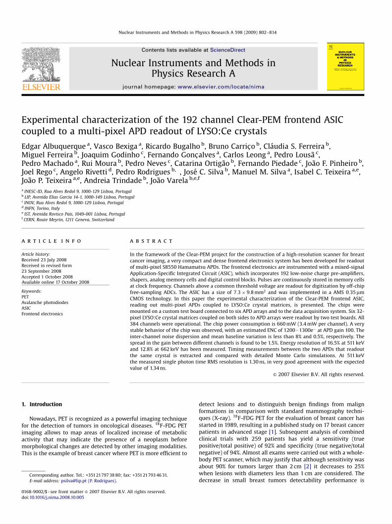
Fig. 2. Closeup photograph of the Clear-PEM chip bonded to the test board.
E. Albuquerque et al. / Nuclear Instruments and Methods in Physics Research A 598 (2009) 802–814 805
risk of coupling digital noise to the amplifier inputs. The targetchip power consumption is about 600–700 mW. The differentialanalog dataframes are digitized by free-sampling dual 10-bit ADCswith differential inputs, clocked at a fixed phase shift in relation tothe ASIC input clock. The phase shift is controlled by the ASICthrough a clock skew delay. The digital data are then carried overa 40-bit bus, plus the channel identifiers, to a LVDS ‘‘Channel Link’’48:8 bit chip that serializes the data. After the contribution fromthe ADCs, ‘‘Channel Link’’ serializer and LVCMOS/LVDS logic levelconverters, assuming a 50 MHz master clock, is taken into accountthe total power consumption per detector head is 55 W.
In the course of the construction of the Clear-PEM scanner,three ASIC versions were produced. The first version was a multi-purpose development chip which includes in the same die severalfunctionalities: 32 input channel amplification circuit withindividual access points; two fully instrumented channels withamplification and digital control circuit, but also with individualaccess points; a complete 32:2 amplification/multiplexing circuit.Experimental tests have allowed to successfully validate theanalog memory and digital controls up to 100 MHz workingfrequency, but the amplifier was found to require changes [20].This was addressed in the second prototype version, whichincluded a revised version of the amplifiers. Several experimentaltests and quality control testbenches were carried out thatdemonstrate that all major requirements were successfullyachieved. The measured gain was 23 mV/fC. The successfulconclusions of the characterization tests of the second prototype
allowed to start the development of the final ASIC fullyinstrumented with 192 input channels. About 170 ASICs wereproduced by Europratice in AMS (Austriamicrosystems) 0:35mmCMOS process. In Fig. 2 a closeup photograph of a die directlybonded on a test board PCB is shown.
3. Experimental results
3.1. Characterization setup
The experimental testbench that was setup to characterize thefrontend chip uses the different electronic sub-systems developedfor the Clear-PEM scanner. A test board for the ASICs was designedwith six layers, having components on both the top and bottomlayers (Fig. 3). Careful layout policies of ground planes for analogand digital were followed in order to avoiding coupling of digitalnoise with the analog section of the ASIC as well as with the APDHV bias supply lines. The test board has all the main componentsof the final FEBs as well as some testability features like thecapability to disable each one of the six blocks of 32 amplifierchannels by putting all the amplifiers inputs at the referencevoltage ðþ3:3 VÞ. The ASIC die is directly bonded into the PCB. Theboard has six low-profile connectors in which the S8550 APDs areplugged-in. The differential analog outputs of the ASIC are routedto a �1 V differential dual 10-bit ADC. The differential LVDS ASICdigital outputs that carry the digital identifier are translated to a

ARTICLE IN PRESS
ASIC
ADC
Ser Chip
Fig. 3. Photograph of the Clear-PEM ASIC test board, with one ASIC die bonded to the PCB. Free-sampling ADC and Channel Link serializer chip are pointed out. APD
connectors placed in the bottom side of the PCB (not shown).
HV
HV
LV
LV
ASIC 0
ASIC 1
ServiceBoard
Data
Data
CLOCK and SYNCFanoutBoard
L1 DataAcquisitionElectronics
Crate
L2 SoftwareTrigger
16
8
16
HV LVI2C
Oscilloscopes
AnalogueDifferentialOutputs
DigitalDifferentialOutputs4 4
CLOCK and SYNC CLOCK and SYNC
Temperature
Temperature
Fig. 4. Schematic representation of the Clear-PEM ASIC test setup.
E. Albuquerque et al. / Nuclear Instruments and Methods in Physics Research A 598 (2009) 802–814806
þ3:3 V LVCMOS level and fed in parallel with the ADC LVCMOSdigital outputs to the serializer chip. The differential analog anddigital outputs are also available in eight LEMO00 single-endedconnectors with a 50 Ohm adaptation, allowing the direct readingof the ASIC activity in an oscilloscope. The input clock, for the testsdescribed in this paper was set to 50 MHz. The system clock isgenerated in the L1 data acquisition electronics TGR/DCC board(Fig. 6) and fanout by a dedicated board that translates the LVPECLclock to LVDS level, before arrival to the test board (Fig. 4). Theoutput LVDS clock of the ASIC is then converted to LVCMOS clockand is used to drive the ADC and the serializer chip. In order toguarantee that the ADCs will sample the analog pulse in a stableregion instead of the sharp transitions, some trial-and-error trialswere carried out by changing the resistor that controls the ASICclock output skew in relation to the analog samples. A delay of
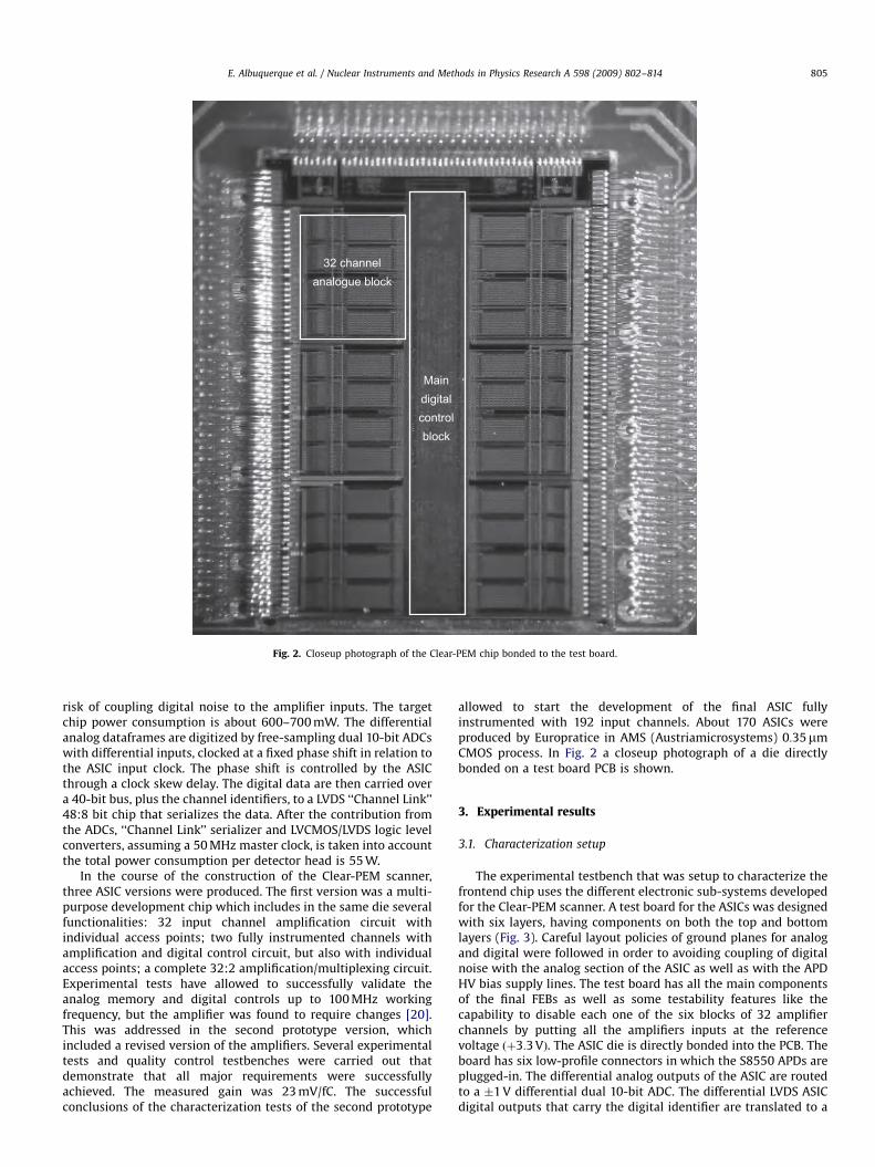
about 4 ns was used for the reported tests. In the Clear-PEMscanner heat dissipated by the ASICs, ADC and serializers isremoved by means of water cooled dissipation plates in thermalcontact with the FEBs. In the tests reported in this paper, the ASICsdies were covered by a temporary glass cover since the step ofcovering the die with a thermally conductive epoxy adhesive(glob-top) had not been performed. This has prevented the usageof a suitable cooling system. Instead cold air was directed to theboard avoiding the uncontrolled heating of the APDs. Using thisapproach the temperature measured under the PCB regionunderlying the APDs was 24226 �C. Two test boards were usedto readout the six Hamamatsu S8550 APDs from each side of a setof six LYSO:Ce crystal arrays, each one with 32 pixels, forming astructure called ‘‘Trigger Cell’’, which defines the basic readoutelement in the Clear-PEM scanner (Figs. 4 and 5). The serialized
ARTICLE IN PRESS
LV, HV and clock cabling
Analogue and digitalspy outputs
ASIC
ASIC
2 x 3 double readoutdetector modules
Fig. 5. Photograph of the ‘‘Trigger Cell’’ setup, with two ASIC test boards reading six Hamamatsu S8550 APDs coupled to detector modules containing a total of 192
2� 2� 20 mm3 LYSO:Ce crystals.
DAQ Boards
TGR/DCC BoardFedKit Transmitter
FedKit Merger
FedKit PCI-X 64 bit 66 MHz G3
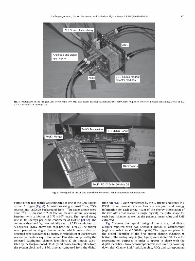
Fig. 6. Photograph of the L1 data acquisition electronics. Main components are pointed-out.
E. Albuquerque et al. / Nuclear Instruments and Methods in Physics Research A 598 (2009) 802–814 807
output of the test boards was connected to one of the DAQ Boardsof the L1 trigger (Fig. 6). Acquisitions using external 22Na, 137Cssources and LYSO:Ce background from 176Lu radioisotope weredone. 176Lu is present in 2.6% fraction mass of natural occurringLutetium with a lifetime of 3:73� 1010 years. The typical decayrate is 300 decays per cubic centimeter of LSO:Ce [21,22]. Thecommon threshold Vth was initially set at 1.55 V (equivalent to� 120 keV), 56 mV above the chip baseline (1.49 V). The triggerwas operated in single photon mode, which means that allaccepted events above the L1 energy threshold (set at 200 keV) arereadout to the data acquisition server. Raw data, composed by thecollected dataframes, channel identifiers, 17-bit timetag calcu-lated by the DAQ on-board FPGAs (9-bit coarse timetag taken fromthe system clock and a 8-bit timetag computed from the digital
time filter [23]), were reprocessed by the L2 trigger and stored in aROOT TTree format. TTree files are analyzed and energyinformation for each crystal (sum of the energy information ofthe two APDs that readout a single crystal), the pulse shape foreach input channel as well as the pedestal mean value and RMSextracted.
Fig. 7 shows the typical timing of the analog and digitaloutputs captured with two Tektronix TDS6804B oscilloscopes(eight channels in total, 500 MSample/s). The trigger was placed inthe digital identifier of the first output channel (Channel 0,bottom). The analog outputs (top figure) were shifted 10 clocks forrepresentation purposes in order to appear in phase with thedigital identifiers. Power consumption was measured by poweringdown the ‘‘Channel Link’’ serializer chip, ADCs and corresponding

ARTICLE IN PRESS
Fig. 7. Oscilloscope captures of the Clear-PEM ASIC: differential analog outputs (top) and digital identifiers (bottom) outputs.
E. Albuquerque et al. / Nuclear Instruments and Methods in Physics Research A 598 (2009) 802–814808
LVCMOS-LVDS logic level converters. Measured power consump-tion at 50 MHz was 660 mW or 3.4 mW per channel, in goodagreement with the targeted specifications.
3.2. Pedestal and noise characterization
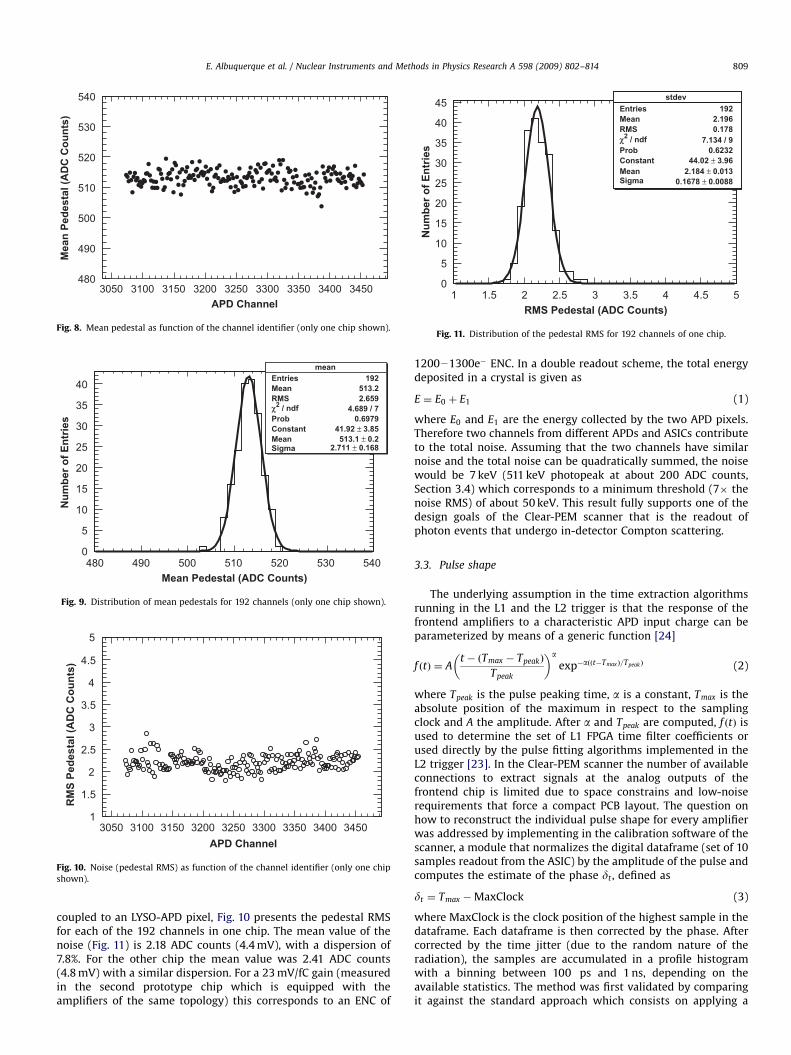
Quantification of the mean pedestal and chip noise (pedestalRMS) were obtained by reprocessing in off-line mode thedataframes acquired by the L1 trigger. The first pre-sample wasextracted from each digital dataframe and binned in differenthistograms, one per channel. Fig. 8 shows the mean pedestal for192 channels for one of the two ASICs (results are similar for theother ASIC in the second test board). The mean value was 513 ADC
counts. The standard deviation of the baselines among the 192channels is 2.7 ADC counts (Fig. 9). The dispersion on the meanvalue is therefore very low, less than 0.5% of the baseline. Sincethe Vth threshold is common to all 192 channels in a single chip,the pedestal stability is a very important parameter since a largeinter-channel variation would force the use of a high Vth reducingthe dynamic range of the chip. Since the adopted ADC is a 10-bit,differential input, from �1 to þ1 V, the 511 ADC count corre-sponds to 0 V. In this configuration, the standard deviation of themean pedestal is around 5.4 mV. The result compares well withthe predicted 8.6 mV value obtained from dedicated Monte Carlosimulations that take into account process and mismatchvariations in the chip production. Regarding the chip noise when
ARTICLE IN PRESS
APD Channel3050 3100 3150 3200 3250 3300
Mea
n Pe
dest
al (A
DC
Cou
nts)
480
490
500
510
520
530
540
3350 3400 3450
Fig. 8. Mean pedestal as function of the channel identifier (only one chip shown).
mea n
Prob
Mean Pedestal (ADC Counts)480
Num
ber o
f Ent
ries
0
5
10
15
20
25
30
35
40
meanEntries 192Mean 513.2RMS 2.659χ2 / ndf 4.689 / 7Prob 0.6979Constant 41.92 ± 3.85Mean 513.1 ± 0.2Sigma
490 500 510 520 530 540
2.711 ± 0.168
Fig. 9. Distribution of mean pedestals for 192 channels (only one chip shown).
APD Channel3050 3100 3150 3200 3250 3300
RM
S Pe
dest
al (A
DC
Cou
nts)
1
1.5
2
2.5
3
3.5
4
4.5
5
3350 3400 3450
Fig. 10. Noise (pedestal RMS) as function of the channel identifier (only one chip
shown).
stdevEntries 192Mean 2.196RMS 0.178χ2 / ndf 7.134 / 9Prob 0.6232Constant 44.02 ± 3.96Mean 2.184 ± 0.013Sigma 0.1678 ± 0.0088
RMS Pedestal (ADC Counts)1
Num
ber o
f Ent
ries
0
5
10
15
20
25
30
35
40
45
1.5 2 2.5 3 3.5 4 4.5 5
Fig. 11. Distribution of the pedestal RMS for 192 channels of one chip.
E. Albuquerque et al. / Nuclear Instruments and Methods in Physics Research A 598 (2009) 802–814 809
coupled to an LYSO-APD pixel, Fig. 10 presents the pedestal RMSfor each of the 192 channels in one chip. The mean value of thenoise (Fig. 11) is 2.18 ADC counts (4.4 mV), with a dispersion of7.8%. For the other chip the mean value was 2.41 ADC counts(4.8 mV) with a similar dispersion. For a 23 mV/fC gain (measuredin the second prototype chip which is equipped with theamplifiers of the same topology) this corresponds to an ENC of
120021300e� ENC. In a double readout scheme, the total energydeposited in a crystal is given as
E ¼ E0 þ E1 (1)
where E0 and E1 are the energy collected by the two APD pixels.Therefore two channels from different APDs and ASICs contributeto the total noise. Assuming that the two channels have similarnoise and the total noise can be quadratically summed, the noisewould be 7 keV (511 keV photopeak at about 200 ADC counts,Section 3.4) which corresponds to a minimum threshold (7� thenoise RMS) of about 50 keV. This result fully supports one of thedesign goals of the Clear-PEM scanner that is the readout ofphoton events that undergo in-detector Compton scattering.
3.3. Pulse shape
The underlying assumption in the time extraction algorithmsrunning in the L1 and the L2 trigger is that the response of thefrontend amplifiers to a characteristic APD input charge can beparameterized by means of a generic function [24]
f ðtÞ ¼ At � ðTmax � TpeakÞ
Tpeak
� �aexp�aððt�TmaxÞ=TpeakÞ (2)
where Tpeak is the pulse peaking time, a is a constant, Tmax is theabsolute position of the maximum in respect to the samplingclock and A the amplitude. After a and Tpeak are computed, f ðtÞ isused to determine the set of L1 FPGA time filter coefficients orused directly by the pulse fitting algorithms implemented in theL2 trigger [23]. In the Clear-PEM scanner the number of availableconnections to extract signals at the analog outputs of thefrontend chip is limited due to space constrains and low-noiserequirements that force a compact PCB layout. The question onhow to reconstruct the individual pulse shape for every amplifierwas addressed by implementing in the calibration software of thescanner, a module that normalizes the digital dataframe (set of 10samples readout from the ASIC) by the amplitude of the pulse andcomputes the estimate of the phase dt , defined as
dt ¼ Tmax �MaxClock (3)
where MaxClock is the clock position of the highest sample in thedataframe. Each dataframe is then corrected by the phase. Aftercorrected by the time jitter (due to the random nature of theradiation), the samples are accumulated in a profile histogramwith a binning between 100 ps and 1 ns, depending on theavailable statistics. The method was first validated by comparingit against the standard approach which consists on applying a
ARTICLE IN PRESS
-20 0
Am
plitu
tde
(mV)
020406080
100120140
PulseReconstructed Pulse
Ped
esta
l
Sco
pe B
asel
ine
-0.6 -0.4 -0.2
Rec
onst
ruct
ed δ
t(C
lock
Uni
ts)
-0.6
-0.4
-0.2
0
0.2
0.4
0.6
20 40 60 80 100Time (ns)
0.2 0.4 0.6δt (Clock Units)
0
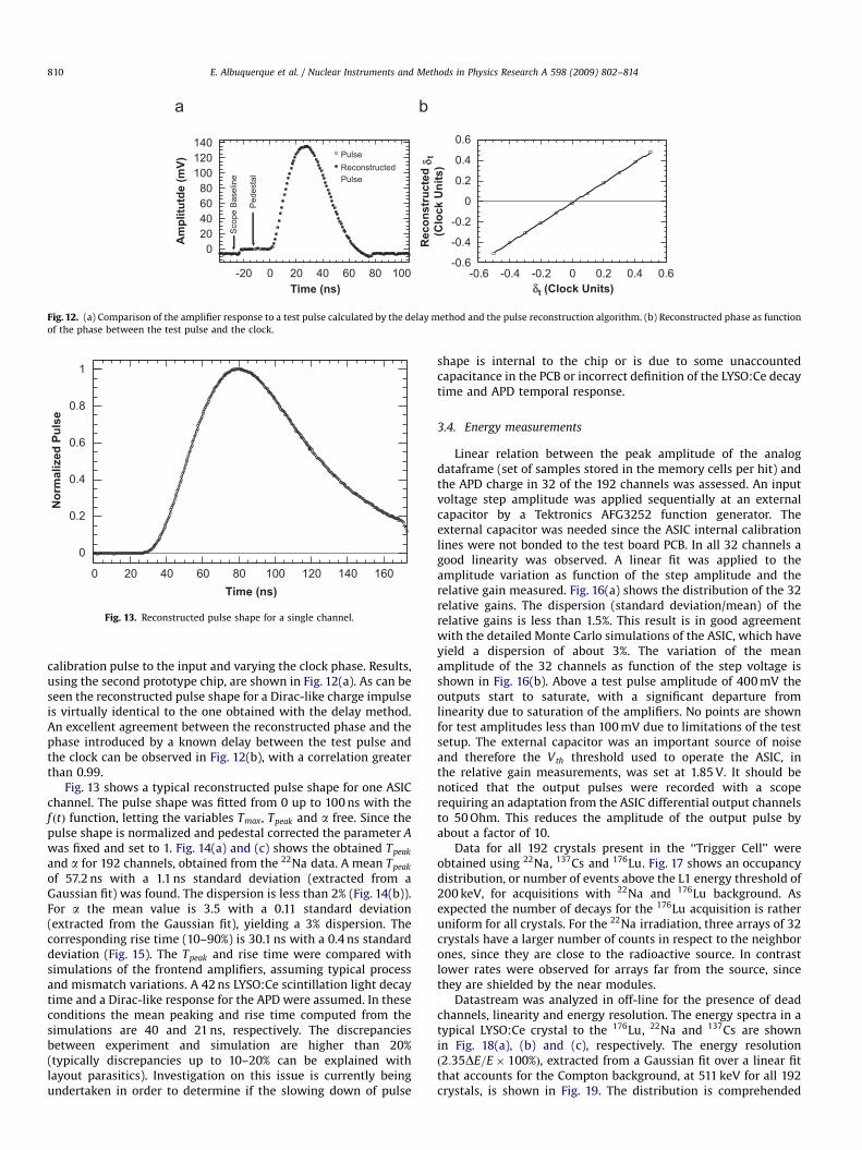
Fig. 12. (a) Comparison of the amplifier response to a test pulse calculated by the delay method and the pulse reconstruction algorithm. (b) Reconstructed phase as function
of the phase between the test pulse and the clock.
0
Nor
mal
ized
Pul
se
0
0.2
0.4
0.6
0.8
1
20 40 60 80 100 120 140 160Time (ns)
Fig. 13. Reconstructed pulse shape for a single channel.
E. Albuquerque et al. / Nuclear Instruments and Methods in Physics Research A 598 (2009) 802–814810
calibration pulse to the input and varying the clock phase. Results,using the second prototype chip, are shown in Fig. 12(a). As can beseen the reconstructed pulse shape for a Dirac-like charge impulseis virtually identical to the one obtained with the delay method.An excellent agreement between the reconstructed phase and thephase introduced by a known delay between the test pulse andthe clock can be observed in Fig. 12(b), with a correlation greaterthan 0.99.
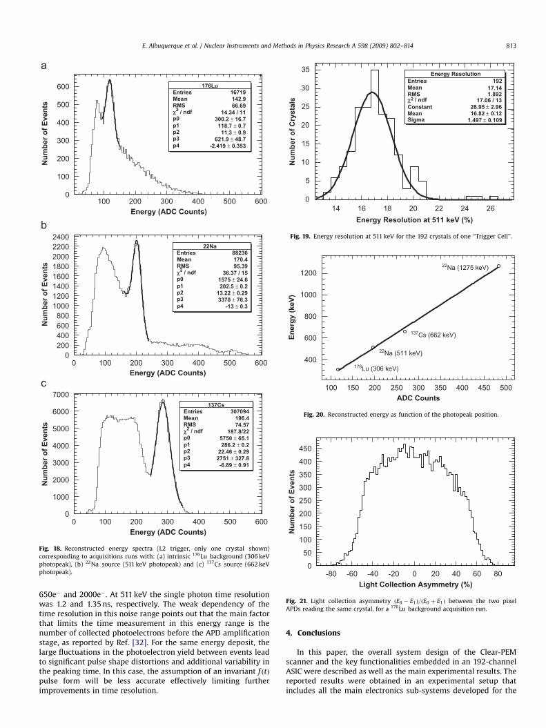
Fig. 13 shows a typical reconstructed pulse shape for one ASICchannel. The pulse shape was fitted from 0 up to 100 ns with thef ðtÞ function, letting the variables Tmax, Tpeak and a free. Since thepulse shape is normalized and pedestal corrected the parameter A
was fixed and set to 1. Fig. 14(a) and (c) shows the obtained Tpeak
and a for 192 channels, obtained from the 22Na data. A mean Tpeak
of 57.2 ns with a 1.1 ns standard deviation (extracted from aGaussian fit) was found. The dispersion is less than 2% (Fig. 14(b)).For a the mean value is 3.5 with a 0.11 standard deviation(extracted from the Gaussian fit), yielding a 3% dispersion. Thecorresponding rise time (10–90%) is 30.1 ns with a 0.4 ns standarddeviation (Fig. 15). The Tpeak and rise time were compared withsimulations of the frontend amplifiers, assuming typical processand mismatch variations. A 42 ns LYSO:Ce scintillation light decaytime and a Dirac-like response for the APD were assumed. In theseconditions the mean peaking and rise time computed from thesimulations are 40 and 21 ns, respectively. The discrepanciesbetween experiment and simulation are higher than 20%(typically discrepancies up to 10–20% can be explained withlayout parasitics). Investigation on this issue is currently beingundertaken in order to determine if the slowing down of pulse
shape is internal to the chip or is due to some unaccountedcapacitance in the PCB or incorrect definition of the LYSO:Ce decaytime and APD temporal response.
3.4. Energy measurements
Linear relation between the peak amplitude of the analogdataframe (set of samples stored in the memory cells per hit) andthe APD charge in 32 of the 192 channels was assessed. An inputvoltage step amplitude was applied sequentially at an externalcapacitor by a Tektronics AFG3252 function generator. Theexternal capacitor was needed since the ASIC internal calibrationlines were not bonded to the test board PCB. In all 32 channels agood linearity was observed. A linear fit was applied to theamplitude variation as function of the step amplitude and therelative gain measured. Fig. 16(a) shows the distribution of the 32relative gains. The dispersion (standard deviation/mean) of therelative gains is less than 1.5%. This result is in good agreementwith the detailed Monte Carlo simulations of the ASIC, which haveyield a dispersion of about 3%. The variation of the meanamplitude of the 32 channels as function of the step voltage isshown in Fig. 16(b). Above a test pulse amplitude of 400 mV theoutputs start to saturate, with a significant departure fromlinearity due to saturation of the amplifiers. No points are shownfor test amplitudes less than 100 mV due to limitations of the testsetup. The external capacitor was an important source of noiseand therefore the Vth threshold used to operate the ASIC, inthe relative gain measurements, was set at 1.85 V. It should benoticed that the output pulses were recorded with a scoperequiring an adaptation from the ASIC differential output channelsto 50 Ohm. This reduces the amplitude of the output pulse byabout a factor of 10.
Data for all 192 crystals present in the ‘‘Trigger Cell’’ wereobtained using 22Na, 137Cs and 176Lu. Fig. 17 shows an occupancydistribution, or number of events above the L1 energy threshold of200 keV, for acquisitions with 22Na and 176Lu background. Asexpected the number of decays for the 176Lu acquisition is ratheruniform for all crystals. For the 22Na irradiation, three arrays of 32crystals have a larger number of counts in respect to the neighborones, since they are close to the radioactive source. In contrastlower rates were observed for arrays far from the source, sincethey are shielded by the near modules.
Datastream was analyzed in off-line for the presence of deadchannels, linearity and energy resolution. The energy spectra in atypical LYSO:Ce crystal to the 176Lu, 22Na and 137Cs are shownin Fig. 18(a), (b) and (c), respectively. The energy resolutionð2:35DE=E� 100%Þ, extracted from a Gaussian fit over a linear fitthat accounts for the Compton background, at 511 keV for all 192crystals, is shown in Fig. 19. The distribution is comprehended

ARTICLE IN PRESS
APD Channel3050 3100 3150 3200 3250 3300
Peak
ing
Tim
e (n
s)
46
48
50
52
54
56
58
60
62
64mean
0.4413
46 50 56
Num
ber o
f Ent
ries
0
5
10
15
20
25
30
35EntriesMeanRMS
13.08 / 13Prob
APD Channel3050 3100 3150 3200 3250 3300
Form
Fac
tor α
2.6
2.8
3
3.2
3.4
3.6
3.8
4
4.2
4.4 stdev
2.6 3 3.2 4 4.2
Num
ber o
f Ent
ries
0
5
10
15
20
25
30
35stdev
3.549
24.41 / 15
Peaking Time (ns)
1.117 ± 0.072SigmaMean 57.18 ± 0.09Constant 31.67 ± 3.08
χ2 / ndf
EntriesMeanRMS
Prob
SigmaMeanConstant
χ2 / ndf
1.321
19257.34
192
0.1772
0.0584132.84 ± 3.43
3.519 ± 0.0080.1022 ± 0.0074
3350 3400 3450 48 52 54 58 60 62 64
3350 3400 3450 2.8 3.4 3.6 3.8 4.4Form Factor α
Fig. 14. Pulse shape parameters: (a) pulse peaking time Tpeak as function of the ASIC readout channel, (b) distribution of Tpeak for all 192 channels, (c) a parameter as
function of the ASIC readout channel, (d) distribution of a for all 192 channels.
Rise TimeEntriesMeanRMS χ2 / ndf 3.696 / 10Constant 31.49 ± 2.89Mean 30.15 ± 0.03Sigma 0.386 ± 0.023
28 28.5 29 29.5 30 30.5
Num
ber o
f Ent
ries
0
5
10
15
20
25
30
Pulse Rise Time (ns)31 31.5 32
19230.15
0.3836
Fig. 15. Distribution of pulse rise time (10–90%) for all 192 channels.
E. Albuquerque et al. / Nuclear Instruments and Methods in Physics Research A 598 (2009) 802–814 811
between 14% and 19%, with a mean value of 16.8% and a standarddeviation of 1.5%. The results are similar to the ones obtained withthe Clear-PEM crystal matrices readout by discrete electronicsbased on CREMAT 110 charge sensitive pre-amplifiers, in whichthe mean energy resolution and the standard deviation are,respectively, 15.6% and 1.3% [25].
Linearity of the LYSO-APD-ASIC-ADC readout chain wasassessed by plotting the reconstructed energy in keV as functionof the photopeak position in ADC counts (Fig. 20). A good linearitywas found over the entire energy range. At 511 keV the photopeakposition is at 195 ADC counts or 390 mV (pulse amplitude). ForLYSO:Ce with a decay constant of 40 ns and an amplifier shapingtime of 20 ns only 43% of the light contributes to the pulseamplitude, reducing the effective gain to 10 mV/fC, which resultsin a total charge at 511 keV of 39 fC. Since the APD is operated at abias supply that at room temperature of 24 �C corresponds to again 100, the total input charge generated at APD inputs (sum ofboth APDs) is about 2560 photoelectrons.
In the Clear-PEM scanner the DOI coordinate along the crystallongitudinal axis is determined from the ratio of collected lightbetween the two pixel APDs glued to a given LYSO:Ce 20 mmlong crystal:
z ¼ CiE0 � E1
E0 þ E1(4)
in which Ci is a calibration constant that translates the lightasymmetry to a physical depth, i is the index of the crystal, E0 andE1 are the energy measurements from the two pixel APDs.
A typical distribution of the light collection asymmetry for176Lu decays in one crystal is shown in Fig. 21. This radioisotopedecays through a b� decay followed by a gamma cascade fromnuclear de-excitation. Due to the crystal production process it can

ARTICLE IN PRESS
32
RMS 0.004629χ2 / ndf 0.9636 / 3Constant 11.01 ± 2.72Mean 0.3144 ± 0.0010Sigma 0.004478 ± 0.000891
0.29 0.3 0.32 0.33
Num
ber o
f Am
plifi
ers
0
2
4
6
8
10
0
Out
put P
ulse
Am
plitu
de (m
V)
0
20
40
60
80
100
120
140
Test Pulse Amplitude (mV)Gain (mV Amplitude / mV Test Pulse)0.31 0.34 0.35 100 200 300 400 500 600
gainEntriesMean 0.3138
Fig. 16. (a) Distribution of the relative gain for 32 input ASIC channels, (b) variation of the mean output voltage for 32 channels as function of the amplitude voltage of the
applied test pulse.
1550
Num
ber o
f Eve
nts
/ Cry
stal
104
105
176Lu
22Na106
Crystal ID1600 1650 1700 1750
Fig. 17. Occupancy distribution for all 192 crystals in the ‘‘Trigger Cell’’ for a 176Lu
background and 22Na acquisition.
E. Albuquerque et al. / Nuclear Instruments and Methods in Physics Research A 598 (2009) 802–814812
be assumed that the 176Lu is uniformly distributed throughoutthe crystal. In this case the b� decays along the depth directionare distributed symmetrically and the light collection asymmetrydistribution should be flat, with the exception of the faredges which correspond to the crystal extremities [26]. Ascan be observed in Fig. 21, the light collection asymmetry ratioðE0 � E1Þ=ðE0 þ E1Þ has a dynamic range comprehended between�60% (interactions near the crystal end at �10 mm) and þ60%(interactions near the crystal end at þ10 mm). The asymmetryvariation per millimeter is therefore of about 6% mm�1. This resultindicates that the performance of the frontend system is adequatefor DOI measurements, since an asymmetry per unit length higherthan 4% mm�1 are compatible with a DOI resolution of 2.2 mmFWHM or better [25].
3.5. Time measurements
In most typical exam scenarios in which the Clear-PEM scannerwill be used, a significant fraction (95%) of the radioactive activityinjected into the patient will be distributed outside the FOV. Thescanner will be subject to a flux of single photons up to 2 MHz perdetector head that needs to be discarded as soon as possible in thedata acquisition chain, avoiding the introduction of deadtime thatcould reduce the system efficiency [27]. A good time resolution is
also required to minimize the presence of random events throughthe use of a narrow coincidence window which contribute to acontrast loss and introduction of artifacts in the reconstructedimages [28].
Estimates of the time resolution offered by the LYSO-APD-ASIC-ADC assembly were obtained. Time difference takenbetween the time of the event in the bottom and top APDs thatreadout the same crystal was computed. Events in the 176Lu(306 keV), 22Na (511 and 1275 keV) and 137Cs (662 keV) photopeakregions were selected. To avoid introduction of any bias due to thedouble readout solution, a cut in the asymmetry distribution(Fig. 21) to select events that interacts in the middle of the crystal,from �10% to þ10%, was applied. Experimental results for thetime resolution (standard deviation/
ffiffiffi2p
) are shown in Fig. 22. Theobtained time resolutions were then compared with prior MonteCarlo simulations. The comparison is shown in Fig. 23. Thesimulations where carried out in the energy range of 100–511 keV,well before the chips were delivered from foundry and thereforeno tuning on the input parameters was performed [23]. Thesimulation includes the calculation of the number of collectedoptical photons in each APD pixel, following the temporaldistribution of the LYSO:Ce emission spectra and estimation ofthe photocurrent produced at the outputs of the APD. Factors suchas Poisson fluctuations on the number of generated opticalphotons and the additional variance in the number of emittedoptical photons, given by a constant term independent of thedeposited energy were included in the simulation. Fluctuations ontotal collected charge due to APD excess noise and dark current,variation of quantum efficiency as function of the optical photonwavelength and dependency of gain with quantum efficiencywere considered. The main S8550 APD electrical characterizationparameters were extracted from Refs. [17,18,29,30]. The chip noisewas assumed to be 1300e� ENC. The histogram of the charge pulseis numerical convoluted with the response of the amplifier. Thechip shaper response to a Dirac-like pulse is provided as anexternal input, previously computed from detailed ASIC simula-tions. At each clock cycle the output pulse is sampled and thecorresponding amplitude stored in a 10 bin-depth vector,emulating the chip analog memories. Simulated dataframes arethen processed by a bit-like Cþþ simulation of the FPGAfirmware [31] and fed into the L2 software trigger.
At 511 keV the experimental single photon time resolution is1.30 ns, in good agreement with the Monte Carlo value of 1.34 ns.Monte Carlo simulations were also carried out for an ASIC noise of
ARTICLE IN PRESS
EnergyResolution291 E
Mean 17.14RMS 1.892
/ ndf 2χ 17.06 / 13Constan .2 t 96± 28.95 Mean 0.12± 16.82 Sigma 0.109± 1.497
Energy Resolution at 511 keV (%)20 22 24 2614 16 18
Num
ber o
f Cry
stal
s
0
5
10
15
20
25
30
35Energy Resolution
291 EntriesMean 17.14RMS 1.892
/ ndf 2χ 17.06 / 13Constan .2 t 96± 28.95 Mean 0.12± 16.82 Sigma 0.109± 1.497
Fig. 19. Energy resolution at 511 keV for the 192 crystals of one ‘‘Trigger Cell’’.
100 300 350
Ener
gy (k
eV)
400
600
800
1000
1200
ADC Counts150 200 250 400 450 500
176Lu (306 keV)
22Na (511 keV)
137Cs (662 keV)
22Na (1275 keV)
Fig. 20. Reconstructed energy as function of the photopeak position.
-80 20
Num
ber o
f Eve
nts
0
50
100
150
200
250
300
350
400
450
Light Collection Asymmetry (%)-60 -40 -20 0 40 60 80
Fig. 21. Light collection asymmetry ðE0 � E1Þ=ðE0 þ E1Þ between the two pixel
APDs reading the same crystal, for a 176Lu background acquisition run.
Entries 16719Mean 142.9RMS 66.69χ2 / ndf 14.34 / 11p0 300.2 ± 16.7p1 118.7 ± 0.7p2 11.3 ± 0.9p3 621.9 ± 48.7p4 -2.419 ± 0.353
100 300 400
Num
ber o
f Eve
nts
0
100
200
300
400
500
600 176Lu
Entries 88236Mean 170.4RMS 95.39χ2 / ndf 36.37 / 15p0 1575 ± 24.6p1 202.5 ± 0.2p2 13.22 ± 0.29p3 3370 ± 76.3p4 -13 ± 0.3
22Na
Entries 307094Mean 196.4RMS 74.57χ2 / ndf 187.8/22p0 5750 ± 65.1p1 286.2 ± 0.2p2 22.46 ± 0.29p3 2751 ± 327.8p4 -6.89 ± 0.91
137Cs
0 100 200 400
Num
ber o
f Eve
nts
0200400600800
10001200140016001800200022002400
0 100 200 400
Num
ber o
f Eve
nts
0
1000
2000
3000
4000
5000
6000
7000
200 500 600Energy (ADC Counts)
Energy (ADC Counts)300 500 600
300Energy (ADC Counts)
500 600
Fig. 18. Reconstructed energy spectra (L2 trigger, only one crystal shown)
corresponding to acquisitions runs with: (a) intrinsic 176Lu background (306 keV
photopeak), (b) 22Na source (511 keV photopeak) and (c) 137Cs source (662 keV
photopeak).
E. Albuquerque et al. / Nuclear Instruments and Methods in Physics Research A 598 (2009) 802–814 813
650e� and 2000e�. At 511 keV the single photon time resolutionwas 1.2 and 1.35 ns, respectively. The weak dependency of thetime resolution in this noise range points out that the main factorthat limits the time measurement in this energy range is thenumber of collected photoelectrons before the APD amplificationstage, as reported by Ref. [32]. For the same energy deposit, thelarge fluctuations in the photoelectron yield between events leadto significant pulse shape distortions and additional variability inthe peaking time. In this case, the assumption of an invariant f ðtÞ
pulse form will be less accurate effectively limiting furtherimprovements in time resolution.
4. Conclusions
In this paper, the overall system design of the Clear-PEMscanner and the key functionalities embedded in an 192-channelASIC were described as well as the main experimental results. Thereported results were obtained in an experimental setup thatincludes all the main electronics sub-systems developed for the

ARTICLE IN PRESS
-20 10
Num
ber o
f Eve
nts
(Arb
. Uni
ts)
0
0.2
0.4
0.6
0.8
1176Lu 306 keV22Na 511 keV137Cs 662 keV22Na 1275 keV
Time Difference (ns)-15 -10 -5 50 15 20
Fig. 22. Experimental time coincidence spectra for events selected in the
photopeak region of 306 keV ð176LuÞ, 511 keV ð
22NaÞ, 662 keV ð137CsÞ and
1275 keV ð22NaÞ.
200 800
RM
S Ti
me
Res
olut
ion
(ns)
0
0.5
1
1.5
2
2.5
3
3.5
4
Experimental Data
Energy (keV)400 600 1000 1200
Monte Carlo
Fig. 23. Comparison of measured single photon time (RMS) resolution with Monte
Carlo simulations as function of the photon energy.
E. Albuquerque et al. / Nuclear Instruments and Methods in Physics Research A 598 (2009) 802–814814
scanner and therefore provide a firm indication of the finalperformance of the scanner. The frontend chip is characterized bya low-noise (120021300e� ENC), when coupled to pixel APDswith 10 pF capacitance, that should allow to readout events withenergies down to 50 keV. Single photon time resolutions arecompatible with a 4 ns FWHM coincidence window, essential tominimize the presence of random events. Time as well as theenergy resolution are compatible with the reported measure-ments using discrete electronics which validates the frontend anddata acquisition systems design. A very low dispersion betweenthe 192 baselines supports the adoption of a common voltagethreshold for the entire chip. In summary, an unprecedentedintegration of number of APD channels in a high gain and low-noise frontend system was obtained which paves way for theconstruction of APD pixel-based large scale PET scanners. Basedon the experience obtained with the test boards developed for theevaluation of this chip, the final frontend boards that will equipthe Clear-PEM scanner were produced. A total of 32 frontendboards with 64 chips were tested. Results are present in Ref. [33].
Acknowledgments
The authors wish to acknowledge J. Kaplon from CERN for thereview of the layout of the Clear-PEM ASIC test board. The authors
would like to thank colleagues from the Portuguese PETConsortium and the Crystal Clear Collaboration for their sugges-tions and contribution. The Clear-PEM project is financed by AdI(Agencia de Inovac- ao) and FCT/POSI (Programa OperacionalSociedade da Informac- ao), Portugal. The work of C. Leong, P.Rodrigues and A. Trindade was supported by FCT (Fundac- ao para aCiencia e Tecnologia) under Grants SFRH/BD/31646/2006, SFRH/BPD/37233/2007 and SFRH/BPD/37226/2007. The work of R.Bugalho, B. Carric-o, C.S. Ferreira, R. Moura, C. Ortigao and J.F.Pinheiro was supported by AdI.
References
[1] H. Minn, I. Soini, Eur. J. Nucl. Med. 15 (2) (1989) 61.[2] C. Rose, J. Dose, N. Avril, R.G. 23 (2002) 613.[3] I.N. Weinberg, D. Beylin, V. Zavarzin, S. Yarnall, P.Y. Stepanov, E. Anashkin,
D. Narayanan, D. Dolinsky, K. Lauckner, L.P. Adler, Technol. Cancer Res. Treat. 4(1) (2005) 55.
[4] L. Tafra, Ann. Surg. Oncol. 14 (1) (2007) 3.[5] C.J. Thompson, K. Murthy, Y. Picard, I.N. Weinberg, F.M. Mako, IEEE Trans.
Nucl. Sci. NS-42 (1995) 1012.[6] W.W. Moses, Nucl. Instr. and Meth. A 525 (2004) 249.[7] M.F. Smith, R.R. Raylman, S. Majewski, A.G. Weisenberger, Phys. Med. Biol. 49
(2004) 2437.[8] P. Lecoq, J. Varela, Nucl. Instr. and Meth. A 486 (2002) 1.[9] M.C. Abreu, et al., IEEE Trans. Nucl. Sci. NS-53 (2006) 71.
[10] E. Albuquerque, P. Bento, C. Leong, F. Gonc-alves, J. Nobre, J. Rego, P. Relvas,P. Lousa, P. Rodrigues, I.C. Teixeira, J.P. Teixeira, L. Silva, M.M. Silva, A. Trindade,J. Varela, IEEE Trans. Nucl. Sci. NS-53 (5) (2006) 2704.
[11] L. Pidol, K. Kahn-Harari, B. Viana, E. Virey, B. Ferrand, P. Dorenbos, J.T.M. deHaas, C.W.E. van Eijk, IEEE Trans. Nucl. Sci. NS-51 (3) (2004) 1084.
[12] Y. Shao, R.W. Silverman, R. Farrell, L. Cirignamo, R. Grazioso, K.S. Shah, G. Visser,M. Clajus, T.O. Tumer, S.R. Cherry, IEEE Trans. Nucl. Sci. NS-47 (3) (2000) 1051.
[13] Y. Shao, K. Meadors, R.W. Silverman, R. Farrell, L. Cirignano, R. Grazioso, K.S.Shah, S.R. Cherry, IEEE Trans. Nucl. Sci. NS-49 (3) (2002) 649.
[14] V. Bexiga, et al., Experimental validation and performance analysis of theClear-PEM data acquisition electronics, in: 2008 IEEE Nuclear ScienceSymposium Conference Record, 2008.
[15] V. Brigljevic, et al., FEDkit: a design reference for CMS data acquisition inputs,in: 9th Workshop on Electronics for LHC Experiments, 2003.
[16] Hamamatsu Photonics K.K., Si APD array S8550, Technical data sheet, 2001.[17] M.C. Abreu, P. Amaral, B. Carric-o, M. Ferreira, R. Moura, C. Ortigao, P. Rato,
J. Varela, Nucl. Instr. and Meth. A 576 (1) (2007) 19.[18] J.B. Mosset, Developpement d’un module de detection phoswich LSO/LuYAP
pour le prototype de camera a positrons ClearPET, Ph.D. Thesis, Faculte desSciences de base de lEcole Polytechnique Federale de Lausanne, 2006.
[19] P. Rodrigues, Study and development of the Clear-PEM trigger and dataacquisition system, Ph.D. Thesis, Instituto Superior Tecnico, UniversidadeTecnica de Lisboa, 2007.
[20] M.C. Abreu, et al., First experimental results with the Clear-PEM detector, in:2005 IEEE Nuclear Science Symposium Conference Record, 2005, pp. 2785–2789.
[21] J.S. Huber, W.W. Moses, W.F. Jones, C.C. Watson, Phys. Med. Biol. 47 (2002)3535.
[22] S. Yamamoto, H. Horii, M. Hurutani, K. Matsumoto, M. Senda, Ann. Nucl. Med.19 (2) (2005) 109.
[23] P. Bento, F. Gonc-alves, C. Leong, P. Lousa, J. Nobre, J. Rego, P. Relvas,P. Rodrigues, J.C. Silva, L. Silva, I.C. Teixeira, J.P. Teixeira, A. Trindade, J. Varela,IEEE Trans. Nucl. Sci. NS-53 (4) (2006) 2102.
[24] P. Busson, Digital filtering for ECAL trigger primitives generator, TechnicalReport CMS Note 1999/020, CMS Collaboration, 1999.
[25] P. Amaral, B. Carric-o, M. Ferreira, R. Moura, C. Ortigao, P. Rodrigues, J.C. Silva,A. Trindade, J. Varela, Nucl. Instr. and Meth. A 580 (2007) 1123.
[26] G.C. Wang, J.S. Hubber, W.W. Moses, W.S. Choong, J.S. Maltz, IEEE Trans. Nucl.Sci. NS-51 (3) (2004) 775.
[27] P. Rodrigues, A. Trindade, J. Varela, J. Instr. 2 (2007) P01004.[28] R.R. Raylman, S. Majewski, R. Wojcik, A.G. Weisenberger, B. Kross, V. Popov,
IEEE Trans. Nucl. Sci. NS-48 (3) (2001) 913.[29] J.B. Mosset, S. Saladino, C. Morel, J.F. Loude, Characterisation of arrays of
avalanche photodiodes, Technical Report, IPHE/UNIL, 2002.[30] J.B. Mosset, S. Saladino, J.F. Loude, C. Morel, Nucl. Instr. and Meth. A 504
(2002) 325.[31] C. Leong, P. Bento, P. Lousa, J. Nobre, J. Rego, P. Rodrigues, J.C. Silva,
I.C. Teixeira, J.P. Teixeira, A. Trindade, J. Varela, IEEE Trans. Nucl. Sci. NS-53(3) (2006) 761.
[32] J.-F. Pratte, J. Sachin, G. Deptuch, J. Fried, O. O’Connor, V. Radeka, P. Vaska,C. Woody, D. Schlyer, S. Stoll, S.H. Maramraju, S. Krishnamoorthy, R. Lecomte,R. Fontaine, The RatCAP front-end ASIC, in: 2007 IEEE Nuclear ScienceSymposium Conference Record, 2007, pp. 19–25.
[33] E. Albuquerque, et al., Performance evaluation of a highly integratedAPD/ASIC double-readout supermodule with 768 channels for Clear-PEM,in: 2008 IEEE Nuclear Science Symposium Conference Record, 2008.