experimental investigation of grid connected z …
TRANSCRIPT

Journal of Research in Engineering and Applied Sciences
JREAS, Vol. 2, Issue 03, July 201799
EXPERIMENTAL INVESTIGATION OF GRIDCONNECTED Z-SOURCE INVERTER
1Department of Electrical EngineeringBhivarabai Sawant College of Engineering and Research, Pune, Maharashtra, India
2Software Engineer, Capgemini India
Abstract
The advancements in power electronics have led to maximum utilisation of available renewable source of energy. Z-source inverter (ZSI) has been investigated recently into renewable energy applications, because of its single stage operation. ZSI can perform buck-boost operation in single stage, which is not possible with traditional inverter topologies. ZSI provides a unique state in which the upper and lower switches of the same leg of inverter are ON, which is not permissible in traditional VSI. Experimental investigation of grid connected ZSI has been presented in paper. Practical aspects of selection of Z-source (ZS) impedance network parameters are presented.
Key Words : Z-source inverter, grid connected system, pulse width modulation
1. Introduction
The energy crises have paved way for the emergence of alternative energy resources which includes solar energy, wind energy, etc. The advancements in power electronics have led to maximum utilization of available renewable source of energy [1-3]. The increasing power demand has increased the utilization of Distributed Generation. The DG feeds micro-grid/grid to meet the power demand. The utilities follow a standardized voltage and frequency profile and these specifications have to be met by the DG. The power conditioning of DG is the most important aspect. The power conditioner system should be economical and highly efficient.
The traditional inverters provide buck or boost capability but not both. Traditional inverters with various levels have been discussed in [4]. The voltage generated through use of renewable energy like solar; is DC and it varies with solar irradiance. Thus, the effective utilization of this energy necessitates DC/AC conversion with regulated voltage and frequency which has to be fed to the grid [5-10]. This led to the search for inverters which are able to provide both buck and boost capabilities with regulated output voltage [11]. One of those inverter topologies is the Z-source inverter (ZSI). The Z-source inverter has been analyzed and presented in [12]. The ZSI provides both buck and boost capability with regulated output voltage. The ZSI eliminates the presence of dead time and also becomes an economical inverter topology with reduction in switching losses owing to is buck and boost capability which is obtained due to the presence of a symmetrical impedance network (Z-Source impedance network) which in addition a inverter provide all the advantageous features which were not observed in traditional inverters. This feature of ZSI makes it the best option for grid
1 2Umesh K. Shinde, Suresh Venkatatesan
interconnection [13-14]. The designing of Z-source impedance network parameters is one of the crucial part and is discussed in [15]. Applications of ZSI for residential and smart grid applications has been analyzed and presented in [16-17]. Various boosting techniques for ZSI has been presented [18-19]. The ZSI based grid connected DG systems for Photovoltaic applications have been presented [20-26]. Power fed to the grid must be at unity power factor and with less distortion.
Synchronization of grid is an important issue and thus Phase locked loop (PLL) has been used. PLL generates the fundamental output voltage which is then applied to the closed loop controller, thus the grid frequency is synchronized with the inverter frequency. For this a closed loop controller is designed which incorporates the action of current controller [27]. Experimental investigation of grid connected ZSI has been presented in paper. Practical aspects of selection of Z-source (ZS) impedance network parameters are presented. The hardware parameters such have been studied through their respective manuals.
2. Z -Source Inverter
The problems occurring in traditional VSI and CSI as discussed in previous section can be overcome by using Z-Source inverter. This Z-source impedance network can be implemented for DC/AC-to-DC/AC power conversion. The general structure of Z-source inverter is shown in Figure 1.
Unlike the traditional VSI or CSI, the ZSI has a unique impedance network with split inductor L1, L2 and capacitor C1, C2 connected in X shape as shown in figure.
ISSN (Print) : 2456-6411, ISSN (Online) : 2456-6403

JREAS, Vol. 2, Issue 03, July 2017100
This impedance network coupled with an inverter provides the buck boost capability of the ZSI. The single phase ZSI consists of five switching states. There are two active, two zero and one shoot through state for single phase ZSI. Out of these, the shoot through is the unique state which is responsible for the buck-boost feature of ZSI. This shoot-through zero state is forbidden in the traditional VSI, because it would cause a shoot-through. With the impedance network, the ZSI can advantageously use the shoot through state to boost the voltage. Furthermore, with the ability to handle the shoot through state, the inverter system becomes more reliable. The inductors and capacitors in the Z-source are both energy storage devices, so their value can be optimally designed to ensure small size and low cost.
From the symmetry ZS network,
ISSN (Print) : 2456-6411, ISSN (Online) : 2456-6403
CCC VVV == 11 LLL VVV == 21 (1)
The capacitor voltage and output voltage are derived as
dcdcshnsh
nshC V
D
DV
TT
TV
21
1
-
-=
-= (2)
dco VD
DV
21
1
-
-=
(3)
Where T is non-shoot through time, T is shoot-through nsh sh
time and D is the duty ratio of shoot-through state.
The overall gain is expressed by equation (4).
MBM
MG =
-=
12 (4)
A. Z-Source Component Design
In ZS network values of inductor and capacitor play a very important role. The voltage boost require is depend on shoot through time period but it is also depend on rating of capacitor and inductor if values of Z source network is not calculate properly then require amount of boost is not gain at output side and causes adverse effects in terms of ripples [14-15,28].
Inductor Design
During traditional operation mode the input voltage appears across the capacitor and no voltage appears across the inductor. During shoot-through time, the inductor voltage is same as capacitor voltage and inductor current increases linearly. The job of the inductor is to limit the current ripple during shoot-through state. Inductor value can be calculated as
V DC
IL
+ VL 1 -
C1C2
+ VL 2 -
S1
S 2
S 3
S 4
To LOAD
Fig. 1 : Schematic of Z-Source inverter (ZSI)
0 0.005 0.01 0.015 0.02-1
-0.5
0
0.5
1
Time(sec)
Fig. 2 : Carrier and Modulating signal waveforms forSimple Boost Control
0 1 2 3 4 5 6
x 10-3
-1
0
1
0 1 2 3 4 5 6
x 10-3
0
0.5
1
Sa
0 1 2 3 4 5 6
x 10-3
0
0.5
1
Sb
0 1 2 3 4 5 6
x 10-3
0
0.5
1
Sc
0 1 2 3 4 5 6
x 10-3
0
0.5
1
Time( msec )
Sd
Shoot through
Carrier Vp
Vn
Reference
Fig. 3 : Switching waveforms with shoot-through in SBC
I
VTL sh
D= (5)
where, V is the average voltages of capacitor during both shoot-through and non-shoot-through time andDI is the assumed current ripple of the inductor.
Capacitor Design
The capacitor absorbs the current ripple and achieves quite a stable voltage. The inductor is charged by the capacitor during shoot-through time. The capacitor value can be calculated as
c
shL
V
TIC
D= (6)

JREAS, Vol. 2, Issue 03, July 2017101
where, I is the average current of the inductor and DV is L c
the assumed voltage ripple of the capacitor.
B. Modulation Technique for Z-Source Inverter
To provide shoot through state in the ZSI different boosting techniques is studied. For providing shoot through state in the ZSI simple boost control technique is used as shown in Figure 2.
Two straight lines are used to realize the shoot through duty ratio (D). Whenever the triangular carrier signal is higher than the positive envelope or lower than the negative envelope, the inverter will operate in shoot-through. Otherwise it works as a traditional PWM inverter. Since the value of the positive straight line equals to the maximum of the sinusoidal reference signals and the value of the negative straight line equals to the minimum of the sinusoidal reference signal, then the modulation index (M) and the shoot-through duty ratio (D) are interdependent of each other. The relation between these two parameters is expressed in equation (7).
Fig. 4 : ZSI (a) Inductor current,(b) Capacitor voltage, (c) Inverter voltage
ISSN (Print) : 2456-6411, ISSN (Online) : 2456-6403
MD -=1 (7)
The switching waveforms of SBC are represented Figure 3.
3. Simulation Results
The ZSI for grid connected circuit has been simulated using SIMULINK software. The specifications used simulation are listed in Table 1. The controller is designed, to track a pre-specified quantity capacitor voltage and gird current to the set point references and regulation against disturbances. In case of Z-source inverter shoot through duty ratio and modulation index are the two important control variables available to the designer by means of the buck-boost feature of ZSI can be realized and the desired load voltage can be gained. The control strategy of ZSI connected grid system involves two independent controls namely; AC side control and DC side control.
The DC side control loop involves the control of DC link voltage in order to maintain a constant voltage across the inverter, as the input DC voltage obtained from the DG is of varying nature. The Z-source capacitor voltage needs to be regulated in order to regulate the DC link voltage which would be the input to the inverter. For variations in DG output voltage, the DC link voltage will vary and accordingly the load voltage will vary. Thus, the DC link voltage must be regulated. For this, the Z-source capacitor voltage is taken as the controlling quantity. This voltage is compared with a reference value and this compared quantity is fed to the PI controller, which eventually generates the modulation signal for inserting shoot through in the zero states. Thus, the DC link voltage is controlled effectively by modulation of shoot through duty ratio.
The AC side control loop involves the control of AC side current with reference generation for generating the modulating signal. This control involves comparison of grid current with a reference current and this compared output is fed to a PI controller which in turn generates the modulating signal for generation of PWM signals. The reference current generation is carried out with the use of Phase locked loop (PLL). The PLL provides synchronization of inverter frequency with the grid frequency and also helps in synchronization of inverter current with grid voltage which in turns provides the power factor improvement. An LC filter has been utilized for suppression of harmonics.
Figure 4 represents the inductor current, capacitor voltage and the output voltage of ZSI under steady state conditions. The regulation of grid current with constant input voltage and constant capacitor voltage is represented in Figure 5, where Vgrid represents load voltage and Igrid represents gird current. The grid voltage had been scaled by a factor of 1/8 for better resolution. The DC inductor current and capacitor voltage have ripples that are associated with the output frequency. This simple boost control's obtainable shoot-through duty ratio decreases with the increase of M and the resulting voltage stresses across the device are relatively high.
Table 1Specifications of ZSI based grid connected system
Parameters Values
Grid Specifications 230V (rms), 50Hz
Power Rating of ZSI 3kW
Switching Frequency 10kHz
Z-Source inductor (L1=L2=L) 160μH
Z-Source Capacitor (C1=C2=C) 1000μF
Current limiting inductor 13mH
0.1 0.2 0.3 0.4 0.5
0
100
200
Il(A
)
0.1 0.2 0.3 0.4 0.5400
450
500
Vc
(V)
0.1 0.2 0.3 0.4 0.50
200400600
Time (sec)
Vp
n(V
)

JREAS, Vol. 2, Issue 03, July 2017102
ISSN (Print) : 2456-6411, ISSN (Online) : 2456-6403
0.2 0.25 0.3 0.35 0.4 0.45 0.5349
350
351V
dc(V
)
0.2 0.25 0.3 0.35 0.4 0.45 0.5
400
500
600
Vc
(V)
0.2 0.25 0.3 0.35 0.4 0.45 0.5-50
0
50
Time (sec)
Vgr
id(V
)Ig
rid
(A)
Iloa
d(A
)
Fig. 5 : Grid current regulation with constant input voltageand capacitor voltage, (a) Input voltage, (b) Capacitor
voltage and (c) Grid voltage, Grid current and Load current
4. Experimental Setup
The experimental setup block diagram is shown in Figure 6. Experimental setup requires power circuit, voltage and current measurement circuit, control circuit, and gate driver circuit is composed of six parts.
A. Gate Driver Circuit
A gate driver is a power amplifier that accepts a low-power input from a controller IC and produces a high-current drive input for the gate of a high-power transistor such as an IGBT or power MOSFET. The Toshiba TLP 250, which consists of light emitting diode and an integrated photo detector, is used in gate isolation and driver circuit. This unit is a 8-lead DIP package. TLP 250 is suitable for gate driving circuit of power MOSFET.
S1
S4
S2
S3
L f
Igrid
Grid
Lf
Inverter
DC Source
Voltage Reference
Circuit
Current Measurement
Circuit
dsPIC33EP256 MC 202(PIC Kit 3 Programmer
kit )
Gate Driver IC
(TLP 250 )
Interface Inductors
+
-Vinv
Z-SourceImpedance
network
Fig. 6 : Hardware implementation for ZSIbased grid connected system
B. Grid Voltage and Current Measurement Circuit
For close loop control, grid voltage is required for generating synchronizing signal and grid current is required for current feedback purpose. ADC of the controller cannot take positive value. So an offset of 1.6V is added to the measured voltage and current signal by using operational amplifier LM324, and then these shifted signals are fed to respective ADC channel of the DSP controller.
C. Capacitor Voltage Measurement Circuit
Resistive voltage divider circuit is used to step down the Capacitor DC voltage. This stepped down signal is connected to the ADC channel of the controller. Since capacitor voltage is DC in nature, unlike AC measurements, offset is not required.
D. Control Circuit
A 16-bit digital controller dsPIC33EP256MC202 is used as the main controller for this research. The controller measures grid voltage, grid current and capacitor voltage, and runs main PI controller program to generate PWM signals for inverter.
5. Hardware Results
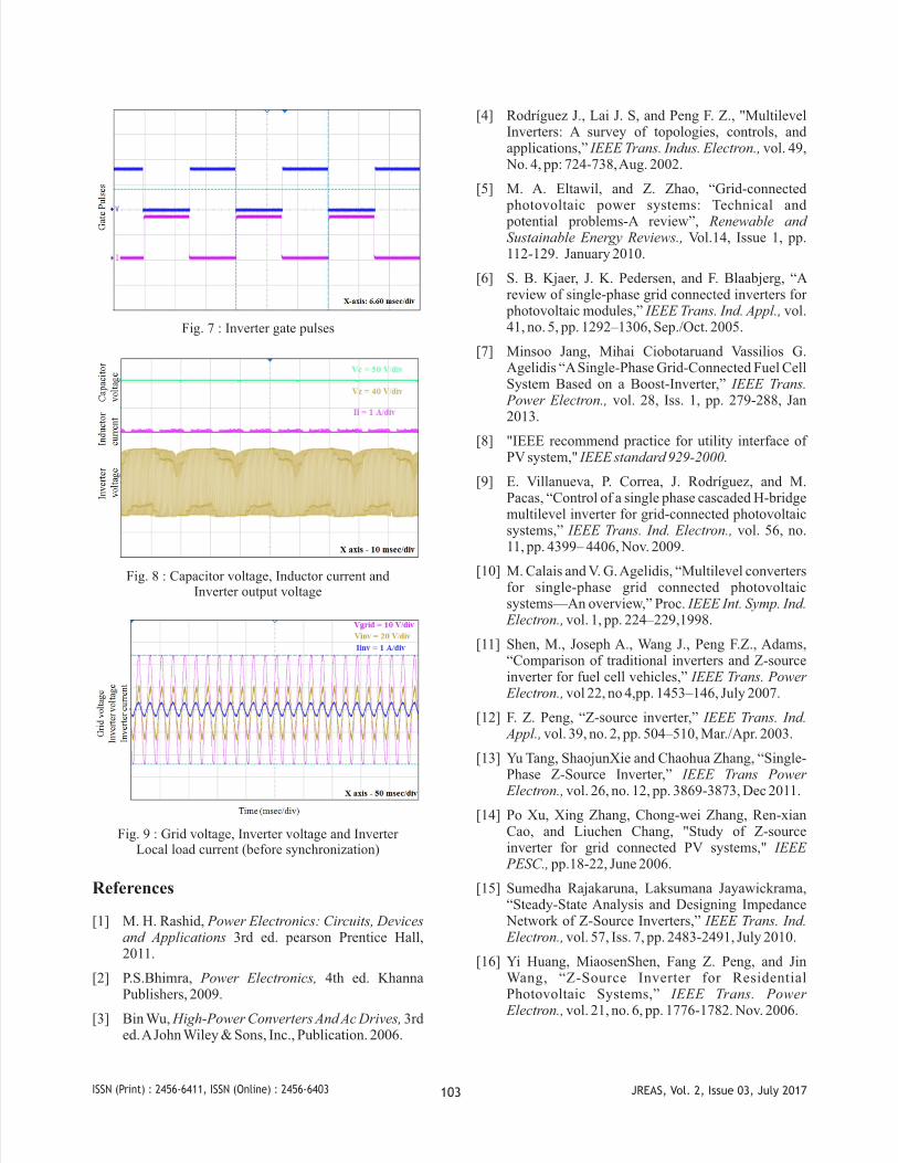
The gate pulses of inverter during non-shoot through configuration, means when input voltage is greater than expected DC link output voltage, are shown in Figure 7. The ZS capacitor voltage, inductor current and inverter output voltage before filter have been represented in Figure 8, corresponding to SBC with modulation index of 0.8 and shoot-through duty ratio of 0.2. Grid voltage, Inverter voltage and Inverter Local load current (before synchronization) are shown in Figure 9.
6. Conclusion
This paper presented simulation results of ZSI with experimental verifications. Single phase H bridge inverter has been used in order to achieve desired specifications with close loop system. The experimental results and circuit simulation results are shown and the simulation results have been verified with the help of measured results. A step by step procedure, for design of implementation of the experimental setup has been explained.
JREAS, Vol. 2, Issue 03, July 2017103ISSN (Print) : 2456-6411, ISSN (Online) : 2456-6403
Fig. 7 : Inverter gate pulses
Fig. 8 : Capacitor voltage, Inductor current andInverter output voltage
Fig. 9 : Grid voltage, Inverter voltage and InverterLocal load current (before synchronization)
References
[1] M. H. Rashid, Power Electronics: Circuits, Devices and Applications 3rd ed. pearson Prentice Hall, 2011.
[2] P.S.Bhimra, Power Electronics, 4th ed. Khanna Publishers, 2009.
[3] Bin Wu, High-Power Converters And Ac Drives, 3rd ed. A John Wiley & Sons, Inc., Publication. 2006.
[4] Rodríguez J., Lai J. S, and Peng F. Z., "Multilevel Inverters: A survey of topologies, controls, and applications,” IEEE Trans. Indus. Electron., vol. 49, No. 4, pp: 724-738, Aug. 2002.
[5] M. A. Eltawil, and Z. Zhao, “Grid-connected photovoltaic power systems: Technical and potential problems-A review”, Renewable and Sustainable Energy Reviews., Vol.14, Issue 1, pp. 112-129. January 2010.
[6] S. B. Kjaer, J. K. Pedersen, and F. Blaabjerg, “A review of single-phase grid connected inverters for photovoltaic modules,” IEEE Trans. Ind. Appl., vol. 41, no. 5, pp. 1292–1306, Sep./Oct. 2005.
[7] Minsoo Jang, Mihai Ciobotaruand Vassilios G. Agelidis “A Single-Phase Grid-Connected Fuel Cell System Based on a Boost-Inverter,” IEEE Trans. Power Electron., vol. 28, Iss. 1, pp. 279-288, Jan 2013.
[8] "IEEE recommend practice for utility interface of PV system," IEEE standard 929-2000.
[9] E. Villanueva, P. Correa, J. Rodríguez, and M. Pacas, “Control of a single phase cascaded H-bridge multilevel inverter for grid-connected photovoltaic systems,” IEEE Trans. Ind. Electron., vol. 56, no. 11, pp. 4399– 4406, Nov. 2009.
[10] M. Calais and V. G. Agelidis, “Multilevel converters for single-phase grid connected photovoltaic systems—An overview,” Proc. IEEE Int. Symp. Ind. Electron., vol. 1, pp. 224–229,1998.
[11] Shen, M., Joseph A., Wang J., Peng F.Z., Adams, “Comparison of traditional inverters and Z-source inverter for fuel cell vehicles,” IEEE Trans. Power Electron., vol 22, no 4,pp. 1453–146, July 2007.
[12] F. Z. Peng, “Z-source inverter,” IEEE Trans. Ind. Appl., vol. 39, no. 2, pp. 504–510, Mar./Apr. 2003.
[13] Yu Tang, ShaojunXie and Chaohua Zhang, “Single-Phase Z-Source Inverter,” IEEE Trans Power Electron., vol. 26, no. 12, pp. 3869-3873, Dec 2011.
[14] Po Xu, Xing Zhang, Chong-wei Zhang, Ren-xian Cao, and Liuchen Chang, "Study of Z-source inverter for grid connected PV systems," IEEE PESC., pp.18-22, June 2006.
[15] Sumedha Rajakaruna, Laksumana Jayawickrama, “Steady-State Analysis and Designing Impedance Network of Z-Source Inverters,” IEEE Trans. Ind. Electron., vol. 57, Iss. 7, pp. 2483-2491, July 2010.
[16] Yi Huang, MiaosenShen, Fang Z. Peng, and Jin Wang, “Z-Source Inverter for Residential Photovoltaic Systems,” IEEE Trans. Power Electron., vol. 21, no. 6, pp. 1776-1782. Nov. 2006.

JREAS, Vol. 2, Issue 03, July 2017104ISSN (Print) : 2456-6411, ISSN (Online) : 2456-6403
[17] M. Hanif, M. Basu and K. Gaughan, “Understanding the operation of a Z-source inverter for photovoltaic application with a design example,” IET Power Electron., vol. 4, Iss. 3, pp. 278 – 287, Feb 2010.
[18] Miaosen Shen, Jin Wang, Member, Alan Joseph, Fang ZhengPeng, Leon M. Tolbert, and Donald J. Adams, “Constant Boost Control of the Z-Source Inverter to Minimize Current Ripple and Voltage Stress”, IEEE Trans. Ind. Appl., vol. 42, no. 3,pp 770-777, May/June 2006.
[19] F. Z. Peng, M. Shen and Z. Qian ,“Maximum Boost Control of the Z-Source Inverter,” IEEE Trans. Power Electron., vol. 20, no. 4, pp. 833-838, July. 2005.
[20] Yu Tang, Jukui Wei, Shaojun Xie, “Grid-tied photovoltaic system with series Z-source Inverter,” IET Renew. Power Gener., vol. 7, Iss. 3, pp. 275–283, Jan2013.
[21] Babak Farhangi, and Shahrokh Farhangi, "Application of Z-source converter in photovoltaic grid-connected transformer-less inverter," Electrical Power Quality and Utilization., Journal., vol. 7, no. 2, pp. 41-45, 2006.
[22] Poh Chiang Loh, D. MahindaVilathgamuwa, YueSen Lai, Geok Tin Chua, and Yunwei Li, “Pulse-Width Modulation of Z-Source Inverters,” IEEE Trans Power Electron., vol. 20, no. 6, pp. 1346-1355, Nov 2005.
[23] Xiaogao Chen and Qing Fu, " PV Grid-connected power conditioning system with Z-source network," Sustainzable Power Generation and Supply, pp.6-7 April, 2009.
[24] C.J. Gajanayake, D.M. Vilathgamuwa, P.C. L.R. Teodorescu, F. Blaabjerg, “Z- Source Inverter Based Flexible Distributed Generation System Solution for Grid Power Quality Improvement,” IEEE Trans. Energy Conver., vol. 24, no. 3, pp. 695-704, Sept 2009.
[25] Hongbin Wu, Hui Sun, Liang Cai, Xiaofeng Tao, “Simulation on Control Strategies of Grid-connected Inverters,” IEEE Int. Symp. Power Electron., distributed generation system., pp. 904-908, 2010.
[26] M.R. Banaei, A.R. Dehghanzadeh, E. Salary, H. Khounjahan, R. Alizadeh, “Z-source-based multilevel inverter with reduction of switches” IET Power Electron., vol. 5, Iss. 3, pp. 385 – 392, October 2011.
[27] T.Chandrashekar and M.Veerachary, “Control of Z-source Inverter Connected to Single-Phase AC Utility System,” Energy and Power Engineering, Journal., vol. 5, pp.447-454, May. 2011.
[28] S. G. Kadwane, M. P. Samarth, and A. H. Deshpande, “Harmonic Analysis of Three Phase Z Source Inverter,” IEEE ICIC Conf., pp. 1288-1293, May. 2015.
[29] Datasheet TLP 250, IRF-840, dsPIC33EP 256MC202 and LM324N.