extended active tunable optical lattice filters enabled by four-dimensional couplers: systems...
TRANSCRIPT
1Ti(Fdsg[Tpgpv
e[awcaptit
osttftiad
El Nagdi et al. Vol. 26, No. 8 /August 2009 /J. Opt. Soc. Am. A A1
Extended active tunable optical latticefilters enabled by four-dimensional
couplers: systems modeling
Amr El Nagdi,1 Louis R. Hunt,1 Duncan L. MacFarlane,1 and Viswanath Ramakrishna2,*1University of Texas at Dallas, Department of Electrical Engineering, P.O. Box 830688, Richardson,
Texas 75083, USA2University of Texas at Dallas, Department of Mathematical Sciences, P.O. Box 830688, Richardson,
Texas 75083, USA*Corresponding author: [email protected]
Received January 8, 2009; accepted March 30, 2009;posted April 20, 2009 (Doc. ID 105802); published June 9, 2009
A system theoretic model of a unit cell of a two-dimensional tunable lattice filter architecture consisting of four4-port couplers and four waveguides containing semiconductor optical amplifiers is provided. It is shown thatsuch multiple input–multiple output devices can be modeled in state space and by transfer function matrices.This modeling can also be extended to devices constructed by concatenations of the basic building block, theunit cell. © 2009 Optical Society of America
OCIS codes: 070.2025, 070.6020, 070.5753, 070.7145, 130.3120.
fitmodtrtfioedq
cfit
tsatt
apcctt
ril
. INTRODUCTIONhis paper is concerned with the system-theoretic model-
ng of an active two-dimensional lattice filter unit celland concatenations thereof). The unit cell is pictured inig. 1. The structure being modeled is a unit cell of a two-imensional active lattice filter architecture consisting ofemiconductor optical amplifiers (SOAs) arranged in arid punctuated by nanoscale photonic 4-port couplers1–5]. In a unit cell there are four such 4-port couplers.his infinite impulse response structure is designed torovide a high-order filter in a minimal photonic inte-rated circuit die area. The SOAs allow movement of filteroles and zeroes with injection current and may also pro-ide high quality factors.
The lattice filter has a long and rich history in math-matics, physical application, and signal processing6–16]. Initially motivated by layered or stratified materi-ls such as geological formations and multiple quantumells, early optical examples were thin-film coatings and
oupled Fabry–Perot etalons. Meanwhile the abstractnalysis of the lattice filter was developed in parallel, anderhaps in isolation [14–16]. The advent of numerical fil-er design tools in signal processing motivated the model-ng, design, and synthesis of optical filters, including lat-ice filters using z-transform techniques [9,10,17].
The lattice filter has traditionally been assumed to bene-dimensional and passive, and the analysis/designpace has been primarily the determination or optimiza-ion of the set of reflection and transmission coefficientshat arise from the signal flow interacting with the inter-aces of the layered structures. Integrated, chip-scale pho-onics naturally motivate the extension of the lattice filternto a second dimenesion using 4-port couplers that havedditional coefficients to split and combine signals in fourirections. As with the traditional one-dimensional lattice
1084-7529/09/0800A1-10/$15.00 © 2
lters, these coupler coefficients influence the position ofhe poles and zeroes of the filter and hence help deter-ine the transfer functions of these multi-input–multi-
utput filters. Passive filters, in contrast to active filters,o not include power gain. The electrical analogy is be-ween filters composed solely of inductors, capacitors, oresistors and those that include vacuum tube or transis-or amplifiers. In the active lattice structure, the ampli-er gains also control the positions of the poles and zeroesf the filter. The authors note the opportunity for two- andven three-dimensional lattice techniques to advance theesign of devices comprising arrays of quantum wires anduantum dots.The architecture of this two-dimensional lattice filter is
hosen to allow high-density, tunable photonic integrationor very high bandwidth signal processing. In particular,t is compatible with a variety of recent advances in pho-onic integrated circuits [18–21].
The adjective “active” refers to the tunability of the sys-em by gains. Not only does this tunability allow for a ver-atile adjustment of filter response, it also enables select-bility of the type of filter implementation. In particular,he gains can be used to place the poles of the filter withinhe unit disk and thereby stabilize the system.
These unit cells can be concatenated. Since the unit cellllows for multiple inputs and outputs (eight each to berecise), concatenations of them will enable further in-rease of the number of inputs and outputs. A typical con-atenation of unit cells is pictured in Fig. 2. The system-heoretic modeling presented in this paper easily extendso a concatenation of unit cells.
The fabrication of the nanophotonic coupler uses a va-iety of nanoscale fabrication techniques such as focusedon beams, inductively coupled plasma etch, and atomicayer deposition. The gains and delays will be imple-
009 Optical Society of America

mt
gcncraorlbNa
fipt4
doi(sd
afsvottl
F2oSt ngular
A2 J. Opt. Soc. Am. A/Vol. 26, No. 8 /August 2009 El Nagdi et al.
ented via SOAs. Further discussion of the fabricationechniques is not the intent of this work.
Couplers are, of course, fundamental to photonic inte-rated circuitry inasmuch as they are used to split and re-ombine signals [6–12,17,22,23]. Four-port couplers sig-ificantly enhance the traditional utility of two-portouplers [1–5]. Accordingly, they are described by moreeflection/transmission type coefficients than go into thenalysis of a two-port coupler. More precisely, at any portf such a coupler, a portion of the incident signal may beeflected, transmitted, routed to the right, or routed to theeft. Thus, each of the four 4-port couplers in a unit cellehaves like a system of coupled transmission lines.ominally each coupler is lossless and thus described byreal orthogonal matrix, viz.,
S = ��W �N �E �S
�W �N �E �S
�W �N �E �S
�W �N �E �S
� . �1�
+
++
+
ρ11S
τ11Sβ11S
α11S
ρ11E
ρ11W
ρ11N β11Nβ11W
β11E
α11N
α11W
α11E
τ11N
τ11E
τ11W
G2
Z-1
+
+
+
+
ρ21S
τ21Sβ21S
α21S
ρ 21E
ρ21W
ρ21N β21Nβ21W
β21E
α21N
α21W
α21E
τ21N
τ21E
τ21W
G4
Z-1
G8 Z-1
G7
Z-1
u5
y1 x3
y8 x4
u7
u1
x6
y7
y2
x8
u3
(U01)
(D21)
(F10)
(F20)
(B10)
(D01)
(U21)
(F10)
(B11)
(B21)
(U11)
(D11)
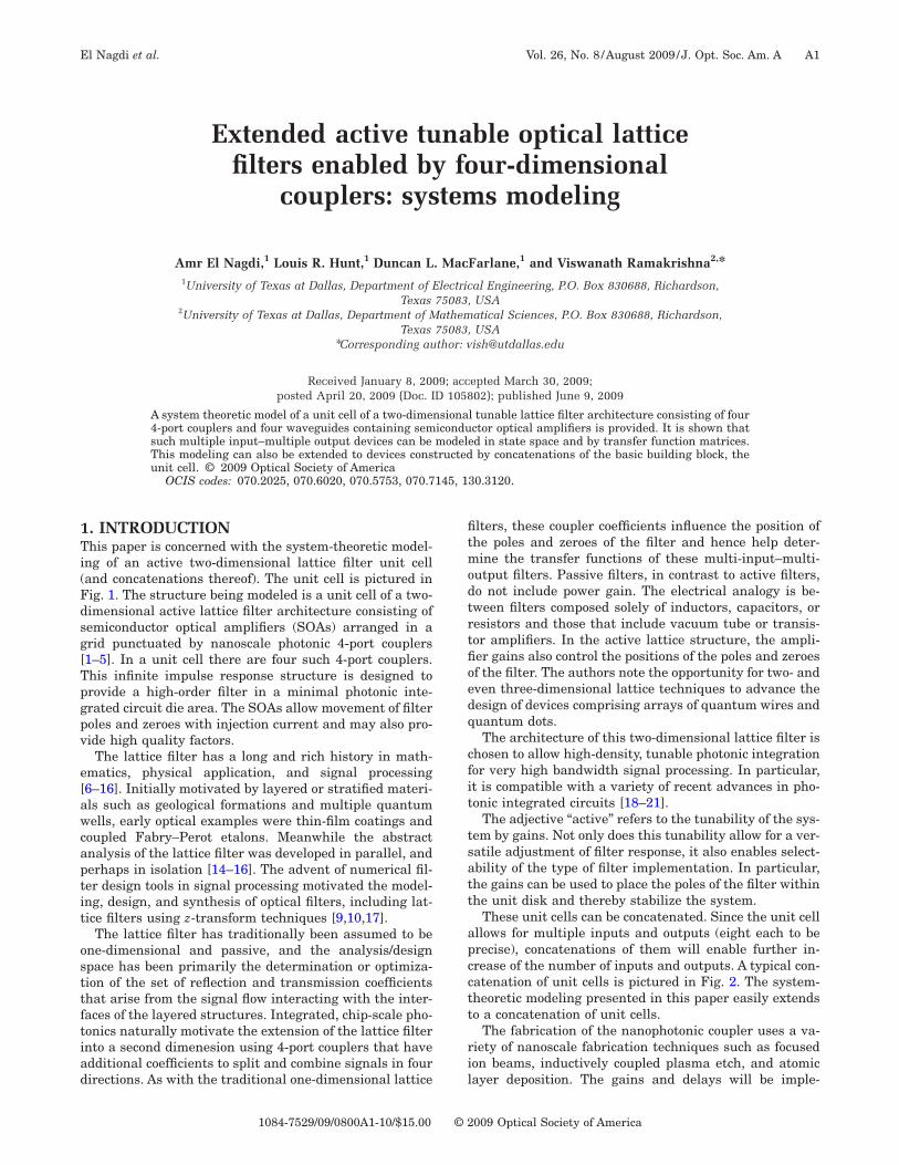
ig. 1. Architecture of the unit cell. The polygonal objects at the1, 22 stand for the 4-port coupler at the southwest, southeast, nus reflection/ transmission type coefficients characterizing each 4matrix [see Eq. (1)] describing the 4-port coupler at the southw
wo 4-port couplers. Similarly the gains are indicated by the tria
The �, �, �, and � are reflection/transmission type coef-cients. The subscripts E, W, N, and S stand for the fourorts in the coupler at which an optical signal is expectedo traverse/recombine. The unit cell consists of these four-port couplers linked to each other via gains and delays.In our earlier paper [5] we had, using quaternions, re-
uced the number of parameters entering the descriptionf a lossless 4-port coupler to six from the original sixteen,.e., explicit equations were provided for the sixteenrelection and transmission type) coefficients � ,� ,� ,� de-cribing the coupler, in terms of six auxiliary parameterserived from two unit quaternions.In this paper we will assume that these coefficients are
lready known, and that they do not necessarily stemrom a lossless device. We will take the gains to be theole quantities that are actively tunable during the de-ice’s operation. Our goal then is to derive an input–utput representation of the unit cell, i.e., we will derivehe transfer matrix and the impulse response matrix ofhe unit cell. The transfer matrix then will be used to il-ustrate the tunability of the device. Moreover, we can
+
+
++
ρ12S
τ12Sβ12S
α12S
ρ12E
ρ 12W
ρ12N β12Nβ12W
β12E
α12N
α12W
α12E
τ12N
τ12E
τ12WG1
Z-1
+
+
+
+
ρ22S
τ22Sβ22S
α22S
ρ22E
ρ22W
ρ22N β22Nβ22W
β22E
α22N
α22W
α22E
τ22N
τ22E
τ22WG3
Z-1
G6 Z-1
G5
Z-1
x1 y4
u6
u8
x2y5
u2
x5
y6
y3
x7
u4
(U02)
(D22)
(B12)
(B22)
(D02)
(F12)
(F22)
(U22)
(F11)
(F21)
(U12)
(D12)
orners of the unit cell are the 4-port couplers. The labels 11, 12,st, and northwest corners of the unit cell, respectively. The vari-oupler are also shown. Thus, �11E stands for the (3,2) entry of therner. The delays are indicated by the square Z−1 blocks between
G blocks in between two 4-port couplers.
four corthea-port cest co

efOa
tthta
2Iummtb
tcltctii
t
bsvtactwa
f
Tiicpdo
mpt
Fcfws
El Nagdi et al. Vol. 26, No. 8 /August 2009 /J. Opt. Soc. Am. A A3
asily generate the frequency response plots of any trans-er function that appears as entry in the transfer matrix.ur modeling yields a state space representation in whichll stability considerations are straightforward.The balance of this paper is organized as follows. Sec-
ion 2 derives the state space model and the transfer func-ion matrix of the unit cell, and also explicitly describesow these can be extended to the analysis of a concatena-ion of unit cells. Section 3 provides two illustrative ex-mples. Section 4 offers conclusions.
. DERIVING TRANSFER FUNCTIONSn this section we derive first the transfer function of thenit cell. Strictly speaking, we should refer to the transferatrix of the unit cell, since the unit cell is a multi-input–ulti-output device. We then point out how transfer ma-
rices of devices consisting of concatenations of the basicuiding blocks can be computed.The methodology to be used to derive the transfer ma-
rix is precisely the state space representation of the unitell. State space representations, popular in the systemsiterature [24], are very versatile and applicable to sys-ems as diverse as those of the electrical, mechanical, orhemical kind. Not only do they enable the derivation ofhe transfer matrix, but they also provide means for test-ng a variety of filter features (such as stability) directlyn terms of the state space representation.
Briefly speaking a discrete (time) state space represen-ation is a model described by the pair of equations
xi
um
ig. 2. (Color online) Two-dimensional lattice filter obtained byouplers. Any signal entering any 4-port coupler at the peripherrom any 4-port coupler at the periphery of the two-dimensionahether they belong to the same unit cell or not) are the states. S
hown.
x�k + 1� = Ax�k� + Bu�k�,
y�k� = Cx�k� + Du�k�. �2�
Here x�Rn ,u�Rm ,y�Rp. In general m ,n ,p will note equal. x is said to be the state of the system. Looselypeaking the state may be thought of as latent or hiddenariables that simplify the passage from the inputs u tohe outputs y, though in several contexts the state vari-bles have concrete physical interpretations. The matri-es A ,B ,C ,D are n�n, n�m, p�n, and p�m, respec-ively. If their entries do not depend on k (as is the caseith the unit cell, for instance), the system is said to beutonomous.Given such a state space representation its transfer
unction matrix is the p�m matrix
G�z� = C�zI − A�−1B + D. �3�
he �i , j�th entry of G�z� is the transfer function describ-ng the effect of the jth input on the ith output. If one isnterested only in the �i , j�th entry, then G�z� need not beomputed entirely. Instead, the jth column of B is multi-lied on the left by �zI−A�−1. Then one computes the stan-ard inner product of the resulting vector with the ith rowf C. To this inner product, Dij is added to find Gij�z�.
The inverse z-transform of G�z� is the impulse responseatrix. Each entry of it is an impulse response. The im-
ulse response matrix can also be explicitly written inerms of the matrices A, B, C, and D. It is given by
yp
enating several unit cells. Several unit cells share certain 4-porte two-dimensional structure is an input. Any signal emanatingture is an output. Signals between 4-port couplers (regardlessillustrative examples of an input, an output, and a state are also
concaty of thl strucample

mcshavcAMbswtbeztotaot
siwn
wttid
poitpabivo
T
T
“etipaahfo
gltfGhst=
ufie(
A4 J. Opt. Soc. Am. A/Vol. 26, No. 8 /August 2009 El Nagdi et al.
H�k� = CAk−1B + D��k�.
The poles of all the transfer functions in the transferatrix, in the absence of pole-zero cancellations, are pre-
isely the eigenvalues of A. If all these eigenvalues aretrictly within the unit disk, i.e., if all the eigenvaluesave modulus strictly smaller than 1, then the system issymptotically stable. If the eigenvalues have absolutealue no larger than 1, and those lying on the unit circleorrespond to simple roots of the minimal polynomial of, then the system is marginally, or Lyapunov, stable.arginal stability means that the state of the system is
ounded in the absence of inputs for any arbitrary initialtate. Asymptotic stability is marginal stability togetherith the stronger requirement that the state converges to
he zero state asymptotically. The desirable attribute ofounded input–bounded output stability (BIBO) isquivalent to asymptotic stability in the absence of pole-ero cancellations in the following sense: if the system’sransfer matrix is proper—i.e., each entry’s numerator isf degree at most equal to that of its denominator—thenhe system is BIBO stable if each pole of the system hasbsolute value strictly smaller than 1. Thus, for a varietyf practical reasons asymptotic stability of the system ishe preferred mode of stability.
A very important point is that coordinate changes intate space leave the transfer function matrix unaltered,.e., if x=Tx for an n�n invertible matrix T, and onerites out the corresponding analog of Eq. (2), then theew transfer function matrix coincides with G�z�.Indeed, the new state space representation is
x�k + 1� = Ax�k� + Bu�k�, y�k� = Cx�k� + Du�k�,
ith A=TAT−1, B=TB, C=CT−1, D=D. Hence the newransfer function matrix C�zI− A�−1B+D coincides withhe old transfer function matrix. For the same reason, thempulse response is not affected by the state space coor-inate changes.State Space Representation of the Unit Cell. We now
resent the state space model for the unit cell. We labelur couplers by (11), (12), (21), (22) (see Fig. 1). Thus, fornstance, the coefficient �11E stands for the (3) and (2) en-ry of the S matrix [see Eq. (1)] describing the 4-port cou-ler labeled (11). With reference to Fig. 1, our input vari-bles are signals entering the unit cell (but not signalsetween the various ports). Similarly, the signals emanat-ng from the unit cell are the outputs, while the stateariables are the signals between one coupler and an-ther.
Explicitly, our inputs are given by
u = �u1,u2,u3,u4,u5,u6,u7,u8�
= �U01,U02,D21,D22,F10,B12,F20,B22�. �4�
he outputs are given by
y = �y1,y2,y3,y4,y5,y6,y7,y8�
= �B10,D01,D02,F12,F22,U22,U21,B20�. �5�
he state is given by
x = �x1,x2,x3,x4,x5,x6,x7,x8�
= �F11,F21,B11,B21,U12,U11,D12,D11�. �6�
The labels B ,F ,U ,D on the various signals stand forback, forward, up, and down,” and may be viewed as anxtension of the notation for signals traveling in a tradi-ional one-dimensional lattice filter [9,10,13–17]. While its clear from Fig. 1 which signals should be deemed in-uts, outputs, or states, the subscript in the label ui ,yj ,xkttached to any of them is arbitrary. However, as we willrgue below, as long as one agrees on the subscripts (and,ence the labels) for the inputs and outputs, the transferunction matrix will not be affected by a different labelingf the states.
The gains are labelled G1 , . . . ,G8. In principle, theains can be allowed to be unequal (as indeed, we will al-ow them in the derivation of the state space model andhe associated A ,B ,C ,D matrices). However, in practice,or technological reasons, we hold that G1=G2, G3=G4,
5=G6, G7=G8. This configuration will be assumed toold when we find the characteristic polynomial of the as-ociated A matrix for the unit cell [see Eq. (14) below]. Ifhere are no gains present, we simply set Gi=1, i1, . . . ,8.A careful inspection of the signal flow in Fig. 1, enables
s to arrive at a state space model for the structure. Therst system of equations below describes how the statevolves, i.e., it is the first of the pair of equations in Eqs.2):
x1�k + 1� = G1��11Nx8�k� + �11Ex3�k� + �11Wu5�k�
+ �11Su1�k��,
x2�k + 1� = G3��21Sx6�k� + �21Ex4�k� + �21Wu7�k�
+ �21Nu3�k��,
x3�k + 1� = G2��12Wx1�k� + �12Nx7�k� + �12Su2�k�
+ �12Eu6�k��,
x4�k + 1� = G4��22Sx5�k� + �22Wx2�k� + �22Eu8�k�
+ �22Nu4�k��,
x5�k + 1� = G6��12Wx1�k� + �12Nx7�k� + �12Eu6�k�
+ �12Su2�k��,
x6�k + 1� = G8��11Ex3�k� + �11Nx8�k� + �11Su1�k�
+ �11Wu5�k��,
x7�k + 1� = G5��22Wx2�k� + �22Sx5�k� + �22Eu8�k�
+ �22Nu4�k��,
x8�k + 1� = G7��21Ex4�k� + �21Sx6�k� + �21Nu3�k�
+ � u �k��. �7�
21W 7
l
t
El Nagdi et al. Vol. 26, No. 8 /August 2009 /J. Opt. Soc. Am. A A5
Next we describe the evolution of the output y, the ana-og of the second of the pair of equations in Eqs. (2):
y1�k� = �11Ex3�k� + �11Nx8�k� + �11Wu5�k� + �11Su1�k�,
y2�k� = �11Ex3�k� + �11Nx8�k� + �11Wu5�k� + �11Su1�k�,
y3�k� = �12Wx1�k� + �12Nx7�k� + �12Eu6�k� + �12Su2�k�,
y �k� = � x �k� + � x �k� + � u �k� + � u �k�,
4 12W 1 12N 7 12E 6 12S 2y5�k� = �22Wx2�k� + �22Sx5�k� + �22Nu4�k� + �22Eu8�k�,
y6�k� = �22Ex2�k� + �22Sx5�k� + �22Nu4�k� + �22Eu8�k�,
y7�k� = �21Ex4�k� + �21Sx6�k� + �21Nu3�k� + �21Wu7�k�,
y8�k� = �21Ex4�k� + �21Sx6�k� + �21Nu3�k� + �21Wu7�k�.
�8�
The above equations for the evolution of the state andhe output thereby yield the following A ,B ,C ,D matrices:
A = �0 0 G1�11
E 0 0 0 0 G1�11N
0 0 0 G3�21E 0 G3�21
S 0 0
G2�12W 0 0 0 0 0 G2�12
N 0
0 G4�22W 0 0 G4�22
S 0 0 0
G6�12W 0 0 0 0 0 G6�12
N 0
0 0 G8�11E 0 0 0 0 G8�11
N
0 G5�22W 0 0 G5�22
S 0 0 0
0 0 0 G7�21E 0 G7�21
S 0 0
� , �9�
B = �G1�11
S 0 0 0 G1�11W 0 0 0
0 0 G3�21N 0 0 0 G3�21
W 0
0 G2�12S 0 0 0 G2�12
E 0 0
0 0 0 G4�22N 0 0 0 G4�22
E
0 G6�12S 0 0 0 G6�12
E 0 0
G8�11S 0 0 G8�11
W 0 0 0 0
0 0 0 G5�22N 0 0 0 G5�22
E
0 0 G7�21N 0 0 0 G7�21
W 0
� , �10�
C = �0 0 �11
E 0 0 0 0 �11N
0 0 �11E 0 0 0 0 �11
N
�12W 0 0 0 0 0 �12
N 0
�12W 0 0 0 0 0 �12
N 0
0 �22W 0 0 �22
S 0 0 0
0 �22W 0 0 �22
S 0 0 0
0 0 0 �21E 0 �21
S 0 0
0 0 0 �21E 0 �21
S 0 0
� , �11�
D = ��11S 0 0 0 �11W 0 0 0
�11S 0 0 0 �11
W 0 0 0
0 �12S 0 0 0 �12
E 0 0
0 �12S 0 0 0 �12
E 0 0
0 0 0 �22N 0 0 0 �22
E
0 0 0 �22N 0 0 0 �22
E
0 0 �21N 0 0 0 �21
W 0
0 0 �21N 0 0 0 �21
W 0
� . �12�

ltdanrt
anmga
wtTttipovtcs
wl
dftiact
Gsh
sctat
ct
sttttcrntnlfiiclbmonta
sccttipew
osbdae(et
ifiuoaseboFtn
am2p
A6 J. Opt. Soc. Am. A/Vol. 26, No. 8 /August 2009 El Nagdi et al.
It is worth emphasizing here that if one agrees on theabels that the various inputs and outputs take, then theransfer function matrix will remain the same, even if oneoes not agree on the labels for the various states. Indeed,relabeling of the states amounts to a state space coordi-ate change effected by a permutation matrix. Hence, asemarked before, this will have no effect on either theransfer function or the impulse response.
It should be noted that while the matrices A ,B ,C ,Dre large, they are sparse. Furthermore, there is a defi-ite pattern to the entries both with regard to their place-ent and indexing. Hence, as the two-dimensional lattice
rows, the construction of these matrices may be readilyutomated.Let us compute the characteristic polynomial of A. We
ill assume, for this purpose, the actual operating condi-ions on the gains, viz., G1=G2, G3=G4, G5=G6, G7=G8.he roots of the characteristic polyomial of A are precisely
he poles of the system. As can be seen below the charac-eristic polynomial is an eighth degree polynomial whichs always even, i.e., only even powers of z appear in theolynomial det�zI8−A�. As a consequence the eigenvaluesf A appear in pairs � ,−�. Furthermore, finding the eigen-alues reduces to computing the roots of a quartic in z2—aask which can be performed in closed form. A simple cal-ulation of pA�z�=det�zI8−A� yields the following expres-ion for it:
pA�z� = �0 + �2z2 + �4z4 + �6z6 + z8, �13�
here the coefficients �i are given by the followingengthy formulas:
�0 = h1G12G3
2G52G7
2,
�2 = h2G12G3
2G52 + h3G1
2G32G7
2 + h4G12G5
2G72 + h5G3
2G52G7
2,
�4 = h6G12G3
2 + h7G12G5
2 + h8G32G5
2 + h9G1G3G5G7
+ h10G12G7
2 + h11G32G7
2 + h12G52G7
2,
�6 = h13G12 + h14G3
2 + h15G52 + h16G7
2. �14�
In the above system the hk, k=1, . . . ,16, are constantsependent on the �, �, �, and �. The explicit expressionsor these are cumbersome, but they are easily found. Notehat if any arbitrary choice of the coefficiets �0, �2, �4, �6s attainable (by appropriately choosing the gains) thenny arbitrary set of eigenvalues (subject, of course, to theondition that if � is in the set then so is −�) is also at-ainable.
It is worth pointing out that even if G1�G2, G3�G4,5�G6, G7�G8, the characteristic polynomial of A would
till be an even polynomial. However, Eqs. (14) would thenave to be modified.Signals versus Controls. In control theory, where state
pace representations are popular, the u is viewed as aontrol with which one may modify the transfer functiono achieve desired characteristics. Typically, this ischieved via feedback control u=Kx, whereby the A ma-rix is modified to A+BK. Unlike state space change of
oordinates such a modification alters the transfer func-ion matrix.
For the problem at hand, however, the u are viewed asignals. They cannot be used to alter the transfer func-ion. What plays the analogous role of controls for the lat-ice filter are the gains Gi. They can be modified in realime by currents. The effect of changing the gains is to al-er the entries of the A and the B matrices. This will, ofourse, alter the transfer function matrix. However, theelation between the gains and the transfer function isot of the standard variety obtained in linear controlheory, i.e., the modification of the system’s A matrix isot of the type A→A+BK. Hence, standard results from
inear control theory cannot be applied to the problem ofnding suitable gains to render the system stable or alter
ts behavior in a specific fashion. For instance, in linearontrol theory it is known that if the system is control-able then, for every polynomial p�x�, there exists a feed-ack control u=Kx such that the characteristic polyno-ial of A+BK is p�x�, i.e., controllability allows the poles
f the system to be chosen arbitrarily. For brevity, we doot discuss the notion of controllability, except to mentionhat a suitable rank test allows one to verify it from the And B matrices of the system [24].For the unit cell being modeled in this work, there is no
uch simple criterion for being able to allow an arbitraryonfiguration of poles for the system. This is primarily be-ause the gains in the unit cell determine the entries ofhe A and B matrices, whereas in linear control theoryhey do not. In fact, the equations to determine the gainsn the unit cell that will achieve a given characteristicolynomial for A form an intricate system of polynomialquations. The analysis of this system is the goal of futureork.Concatenation of Unit Cells. We give an example here
f how the gains can be used to render a “marginally”table system asymptotically stable. This section shoulde read with reference to Figs. 1 and 2. In the state spaceescription of the unit cell, the states, inputs and, outputsll had an equal number of components, viz., eight. How-ver, when one concatenates more than such unit cellssee Fig. 2), one finds that while the number of inputsquals the number of outputs, neither is typically equal tohe number of states.
With reference to Fig. 2, we note that the signals enter-ng the unit cells located on the periphery of the structuregured are the inputs. The signals emanating out of thenit cells located on the periphery are the outputs. Allther signals in the two-dimensional lattice filter picturedre to be viewed as states. In particular, in contrast to theituation for a single unit cell, there are several signalsntering and emanating out of a unit cell that could nowe considered states but not inputs or outputs. Examplesf typical input, output, and state signals are shown inig. 2. Thus, while the number of inputs is the same ashe number of outputs, they both typically differ from theumber of states.The state space description will still be of the same type
s in Eq. (2). We now describe a generic method to deter-ine the entries of A, B, C, and D, with reference to Fig.
. A waveguide begins with a () sign in one 4-port cou-ler and ends with an arrowhead in another 4-port

cgtii
stsFgxspsp
tgsgscptaf4tT
3Iu
a(fbm(tvag
A
St
G+i
F�a
El Nagdi et al. Vol. 26, No. 8 /August 2009 /J. Opt. Soc. Am. A A7
oupler—see Fig. 1. In between there is a unit delay and aain. The delay is subsumed by the �k+1� in x�k+1�. Onhe arrowhead side of the gain the state is labeled xi (i.e.,t is the ith component of x). There are four signals enter-ng the () sign and four signals leaving the arrowhead.
At least two of the inbound signals must be from othertates in other waveguides connected to the first of thewo 4-port couplers in the paragraph above, and any otherignals are from external inputs into that 4-port coupler.rom a state xj we pass through a parameter in the be-inning 4-port coupler to reach the sign leading to statei. This parameter times the gain preceding xi is Aij. If theignal is from an external input um, we pass through thearameter in the beginning 4-port coupler to reach the ign leading to state xi. This parameter times the gainreceding xi is Bim.Now consider the signals leaving the arrowhead after
he state xi. At least two of these emanating signals musto to other states in other waveguides connected to theecond of the two 4-port couplers, while any others musto to the external outputs leaving that 4-port coupler. To atate xn we pass through a parameter in the ending 4-portoupler that emanates from the arrowhead after xi. Thisarameter times the gain preceding xn is, of course, Ani. Ifhe signal goes to an external output yp, we pass throughparameter in the ending 4-port coupler that emanates
rom the arrowhead after xi. This parameter is Cpi. In any-port coupler, a direct signal from an external input umo the external ouput must pass through a parameter.his parameter is Dpm.
ig. 3. SEM image showing the top view of a 4-port coupler ba3 m� is etched in the InP then backfilled with alumina by atom
nd partially coupled evanescently into adjacent waveguides.
. ILLUSTRATIVE EXAMPLESn this section, we illustrate the stability behavior of thenit cell for certain parameter values.Example 1: In the first example the parameters chosen
re the result of extended finite-difference time-domainFDTD) modeling that includes important practicalities ofabrication [25]. The precise structure of the coupler isased on frustrated total internal reflection and is imple-ented as a cross of two thin trenches filled with titania
see Fig. 3). Specifically all the � are set equal to −0.3937,he � to 0.4272, the � to 0.4416, and the � to 0.5595. Thesealues give a high overall efficiency and reasonably bal-nced operation. Furthermore, we initially pick all theains equal to 1.
With these choices the eigenvalues of the correspondingmatrix are
�1 = 0.8282, �2 = − 0.8282, �3 = 0.0406, �4 = − 0.0406, �5
= j0.1908, �6 = − j0.1908, �7 = j0.1764, �8 = − j0.1764.
ince each eigenvalue has absolute value strictly smallerhan 1, the system is asymptotically stable.
As a sample of transfer function calculations, let us find47�z�. This is the (4, 7) entry of the matrix C�zI−A�−1BD and represents the transfer function from the seventh
nput to the fourth output. Explicitly it is
frustrated total internal reflection. A thin deep trench �150 nmr deposition. A wave incident on the coupler is partially reflected
sed onic laye

Is�q4dpsv
W
OuFt
Tit
FS
A8 J. Opt. Soc. Am. A/Vol. 26, No. 8 /August 2009 El Nagdi et al.
�C4R,�zI − A�−1B7
C� + D47
=0.2111z−2 − 0.14z−4 − 0.005z−6
1 − 0.62z−2 − 0.0441z−4 − 0.0007z−6 .
n the above equation, C4R is the fourth row of C, B7
C is theeventh column of B and D47 is the (4, 7) entry of D, and, � stands for the usual inner product of vectors. The fre-uency response (magnitude and phase) are shown in Fig.. Note that the denominator of the G47�z� is only sixthegree in z−1 (and not eighth degree). This inidcates theresence of a pole-zero cancellation. Nevertheless, theystem is asymptotically stable, since all the eight eigen-alues of A are within the open unit disc.
Next, we modify the gains according to
G1 = G2 = 0.2, G3 = G4 = 0.4,
G5 = G6 = 0.6, G6 = G7 = 0.8. �15�
e retain the same values for the �, �, �, and �.
0 0.1 0.2 0.3 0.4-400
-350
-300
-250
-200
-150
-100
-50
0
Normalized
Phase(degrees)
0 0.1 0.2 0.3 0.4-14.1
-14
-13.9
-13.8
-13.7
-13.6
-13.5
-13.4
-13.3
-13.2
-13.1
Normalized
Magnitude(dB)
ig. 4. Magnitude and phase response for the transfer functioection 3 when all the gains are set equal to 1.
Now the eigenvalues of A are
�1 = 0.4188, �2 = − 0.4188, �3 = 0.0146,
�4 = − 0.0146, �5 = 0.0783 + j0.1908,
�6 = 0.0783 − j0.1908, �7 = − 0.0783 + j0.1908,
�8 = − 0.0783 − j0.1908. �16�
nce again all the eigenvalues of A are within the opennit disk, and hence the system is asymptotically stable.or comparison, the (4, 7) entry of the new transfer func-
ion is
0.0422z−2 − 0.0078z−4
1 − 0.186z−2 + 0.0014z−4 .
he frequency response (magnitude and phase) are shownn Fig. 5. The effect of the gain can be most vividly seen inhe magnitude plots.
0.6 0.7 0.8 0.9 1y ( rad/sample)
0.6 0.7 0.8 0.9 1y ( rad/sample)
the seventh input u7 to the fourth output y4 in Example 1 of
0.5Frequenc
0.5Frequenc
n from

acpsag�−
S
T0
cHttza
hp=TSs
4WsOa
FS 8.
El Nagdi et al. Vol. 26, No. 8 /August 2009 /J. Opt. Soc. Am. A A9
Example 2: Next we illustrate the use of the gains tosymptotically stabilize the unit cell. The scenario weonsider is that of equal energy transfer between the fourorts. One configuration of parameter values which en-ures this occurs when all the � are set equal to −0.5 andll the �, �, and � are chosen to be 0.5. We first pick all theains equal to 1. We compute G11�z�. This is d11+ �u ,v, where d11=0.5, u is the first row of C, and v is �zIA�−1 times the first column of B.This yields
G11�z� =0.5 − 0.75z−2 + 0.25z−4
z−6 − z−8 .
imilary,
G12�z� =0.25z−1 − 0.25z−3
z−6 − z−8 .
he eigenvalues of the corresponding A matrix are 1, −1,, 0, 0, 0, 0, 0. The two eigenvalues of A on the unit circle
0 0.1 0.2 0.3 0.4-400
-350
-300
-250
-200
-150
-100
-50
0
Normalize
Phase(degrees)
0 0.1 0.2 0.3 0.4-27.53
-27.52
-27.51
-27.5
-27.49
-27.48
-27.47
-27.46
-27.45
Normalize
Magnitude(dB)
ig. 5. Magnitude and phase response for the transfer functioection 3 when G1=G2=0.2, G3=G4=0.4, G5=G6=0.6, G7=G8=0.
orrespond to simple roots of the minimal polynomial.ence the system is marginally (Lyapunov) stable. Note
hat the roots of the denominator of either transfer func-ion are equal to +1, −1. The fact that the remaining sixero eigenvalues of the A matrix do not appear as roots isn indication of pole-zero cancellation.Let us now change the gains to alter the stability be-
avior. The �, �, �, and � are as before. However, we nowick G1=G2=0.3, G3=G4=0.2, G5=G6=0.7, and G7=G80.9. With this choice, one computes the eigenvalues of A.hese are −0.6903, 0.6903, 0.1970, −0.1970, 0, 0, 0, 0.ince all the eigenvalues have absolute value strictlymaller than 1, the system is asymptotically stable.
. CONCLUSIONSe have shown how to model the unit cell in terms of
tate space and in terms of transfer function matrices.ur modeling methods are illustrated by interesting ex-mples with parameters derived from actual device oper-
5 0.6 0.7 0.8 0.9 1cy ( rad/sample)
5 0.6 0.7 0.8 0.9 1cy ( rad/sample)
the seventh input u7 to the fourth output y4 in Example 1 of
0.d Frequen
0.d Frequen
n from

agr
fistdAsptttsetgmfi
ATDttbitd
R
1
1
1
1
1
1
1
1
1
1
2
2
2
2
2
2
A10 J. Opt. Soc. Am. A/Vol. 26, No. 8 /August 2009 El Nagdi et al.
ting conditions. Stability can be determined from the ei-envalues of the A matrix in the state spaceepresentations.
Future work will consist of deriving necessary and suf-cient conditions to ensure that poles and zeroes of theystem can be placed as desired by appropriately tuninghe gains. Most questions such as stabilization can be re-uced to achieving a given characteristic polynomial for. As mentioned before the equations that the gains mustatisfy so that one can achieve a given eighth degree evenolynomial as the characteristic polynomial for the A ma-rix forms a system of polynomial equations. Each equa-ion in this system turns out to be homogeneous. Tradi-ionally the field of mathematics that addresses theolvability of such systems is projective algebraic geom-try. However, since one is interested in real solutions forhe gains (which furthermore have to be in certain re-ions, so as to respect experimental constraints), theethods of algebraic geometry have to be suitably modi-
ed. This will be addressed in future work.
CKNOWLEDGMENTShe authors gratefully acknowledge the support of theefense Advanced Research Projects Agency (DARPA)
hrough grant HR0011-08-1-005. DARPA has approvedhis manuscript for public release with unlimited distri-ution. We thank Nahid Sultana and Wei Zhou for provid-ng us with the SEM image. We also thank Marc Chris-ensen and Nathan Huntoon for providing us with FDTData used in the examples.
EFERENCES1. D. L. MacFarlane, J. Tong, C. Fafadia, V. Govindan, L. R.
Hunt, and I. Panahi, “Extended lattice filters enabled byfour directional couplers,” Appl. Opt. 43, 6124–6133 (2004).
2. G. Grieffel, “Synthesis of optical filters using ring resonatorarrays,” IEEE Photon. Technol. Lett. 12, 810–812 (2000).
3. D. Hoffman, H. Heidrich, G. Wenke, R. Langenhorst, andE. Dietrich, “Integrated optics eight-port 90 hybird onLiNb03,” J. Lightwave Technol. 7, 794–798 (1989).
4. D. Roh, T. Masood, S. Patterson, N. V. Amarasinghe, S.McWilliams, G. A. Evans, and J. Butler, “Dual-wavelengthAlInGaAs-InP grating-outcoupled surface-emitting laserwith an integrated two-dimensional photonic latticeoutcoupler,” IEEE Photon. Technol. Lett. 17, 270–273(2005).
5. T. Constantinescu, V. Ramakrishna, N. Spears, L. R. Hunt,J. Tong, I. Panahi, G. Kannan, D. L. MacFarlane, G. A.Evans, and M. P. Christensen, “Composition methods forfour-port couplers in photonic integrated circuitry,” J. Opt.Soc. Am. A 23, 2919–2931 (2006).
6. B. Moslehi, J. W. Goodman, M. Tur, and H. J. Shaw, “Fiberoptic lattice signal processing,” Proc. IEEE 72, 909–930(1984).
7. F. J. Fraile-Peláez, J. Capmany, and M. A. Muriel,“Transmission bistability in a double-coupler fiber ringresonator,” Opt. Lett. 16, 907–909 (1991).
8. K. Sasayama, M. Okuno, and K. Habara, “Coherent opticaltransversal filter using silica-based waveguides for highspeed signal processing,” J. Lightwave Technol. 9,1225–1230 (1991).
9. D. L. MacFarlane and E. M. Dowling, “Z-domain
techniques in the analysis of Fabry-Perot etalons andmultilayer structures,” J. Opt. Soc. Am. A 11, 236–245(1994).
0. C. K. Madsen and J. H. Zhao, Optical Filter Design andAnalysis: A Signal Processing Approach (Wiley, 1999).
1. L. R. Hunt, V. Govindan, I. Panahi, J. Tong, G. Kannan, D.L. MacFarlane, and G. A. Evans, “Active optical latticefilters,” EURASIP J. Appl. Signal Process. 10, 1–11 (2005).
2. I. Panahi, G. Kannan, L. R. Hunt, D. L. MacFarlane, and J.Tong, “Lattice filter with adjustable gains and itsapplications in optical signal processing,” 2005 IEEE/SP13th Workshop on Statistical Signal Processing (IEEEPress, 2005), pp. 321–326.
3. J. G. Proakis and D. Manolakis, Digital Signal Processing,Principles, Algorithms and Applications (Prentice Hall,1996).
4. J. Makhoul, “Stable and efficient lattice methods for linearprediction,” IEEE Trans. Acoust., Speech, Signal Process.ASSP-25, 423–428 (1977).
5. J. Makhoul, “A class of all-zero lattice digital filters:Properties and applications,” IEEE Trans. Acoust., Speech,Signal Process. ASSP-26, 304–314 (1978).
6. A. H. Gray, Jr., “Passive cascaded lattice digital filters,”IEEE Trans. Circuits Syst. CAS-27, 337–344 (1980).
7. E. M. Dowling and D. L. MacFarlane, “Lightwave latticefilters for optically multiplexed communication systems,” J.Lightwave Technol. 12, 471–486 (1994).
8. R. Nagarajan, C. H. Joyner, R. P. Schneider, Jr., J. S.Bostak, T. Butrie, A. G. Dentai, V. G. Dominic, P. W. Evans,M. Kato, M. Kauffman, D. J. H. Lambert, S. K. Mathis, A.Mathur, R. H. Miles, M. L. Mitchell, M. J. Missey, S.Murthy, A. C. Nilsson, F. H. Peters, S. C. Pennypacker, J.L. Pleumeekers, R. A. Salvatore, R. K. Schlenker, R. B.Taylor, H. S. Tsai, M. F. Van Leeuwen, J. Webjorn, M. Ziari,D. Perkins, J. Singh, S. G. Grubb, M. S. Reffle, D. G.Mehuys, F. A. Kish, and D. F. Welch, “Large-scale photonicintegrated circuits,” IEEE J. Sel. Top. Quantum Electron.50–65 (2005).
9. R. Nagarajan, M. Kato, V. G. Dominic, C. H. Joyner, R. P.Schneider, Jr., A. G. Dentai, T. Desikan, P. W. Evans, M.Kauffman, D. J. H. Lambert, S. K. Mathis, A. Mathur, M.L. Mitchell, M. J. Missey, S. Murthy, A. C. Nilsson, F. H.Peters, J. L. Pleumeekers, R. A. Salvatore, R. B. Taylor, M.F. Van Leeuwen, J. Webjorn, M. Ziari, S. G. Grubb, D.Perkins, M. Reffle, D. G. Mehuys, F. A. Kish, and D. F.Welch, “400 Gbit/s (10 channel 40 Gbit/s) DWDM photonicintegrated circuits,” Electron. Lett. 41, 1–2 (2005).
0. R. Nagarajan, M. Kato, C. H. Joyner, R. P. Schneider Jr., J.Back, A. G. Dentai, T. Desikan, V. G. Dominic, P. W. Evans,M. Kauffman, D. J. H. Lambert, S. K. Hurtt, A. Mathur, M.L. Mitchell, M. J. Missey, S. Murthy, A. C. Nilsson, F. H.Peters, J. L. Pleumeekers, R. A. Salvatore, R. B. Taylor, M.F. Van Leeuwen, J. Webjorn, M. Ziari, S. G. Grubb, D.Perkins, M. Reffle, D. G. Mehuys, F. A. Kish, and D. F.Welch, “Wide temperature (2585 C) coolerless operation of100 Gbits DWDM photonic integrated circuit,” Electron.Lett. 41, 1–2 (2005).
1. J. Tong, K. Wade, D. L. MacFarlane, S. McWilliams, G. A.Evans, and M. P. Christensen, “Active integrated photonictrue time delay device,” IEEE Photon. Technol. Lett. 18,1720–1722 (2006).
2. Y. Li, C. Henry, E. Laskowski, C. Mak, and H. Yaffe,“Waveguide EDFA gain equalization filter,” Electron. Lett.31, 2005–2006 (1995).
3. D. L. MacFarlane, E. M. Dowling, and V. Narayan, “Ringresonators with NM couplers,” Fiber Integr. Opt. 14,195–210 (1995).
4. C. T. Chen, Linear System Theory and Design (Oxford U.Press, 1999).
5. N. R. Huntoon, M. P. Christensen, D. L. MacFarlane, G. A.Evans, and C. S. Yeh, “Integrated photonic coupler basedon frustrated total internal reflection,” Appl. Opt. 47,
5682–5690 (2008).