fabrication and application of metallic nano-cantilevers
TRANSCRIPT
ARTICLE IN PRESS
0026-2692/$ - se
doi:10.1016/j.m
�CorrespondE-mail addr
Microelectronics Journal 37 (2006) 1306–1312
www.elsevier.com/locate/mejo
Fabrication and application of metallic nano-cantilevers
Anirban Chakrabortya, Cheng Luob,�
aDepartment of Electrical Engineering and Institute for Micromanufacturing, Louisiana Tech University, Ruston, LA 71272, USAbDepartment of Biomedical Engineering and Institute for Micromanufacturing, Louisiana Tech University, Ruston, LA 71272, USA
Received 12 May 2006; accepted 10 July 2006
Available online 23 August 2006
Abstract
A new approach was developed in this work to fabricate metallic nano-cantilevers using a one-mask process and a deep reactive ion
etch (DRIE) technique. 40-nm-thick Al and 70-nm-thick Au cantilevers of lengths from 5mm and widths in the range of 200–300 nm were
fabricated on a silicon substrate. The silicon underneath the suspended beams was completely etched. Short Al nano-cantilevers were
used to find local residual stress induced in rapid thermal oxidation and the oxidized spots according to the deflection profiles of the
nano-cantilevers. The deflection profiles were determined with the aid of a scanning electron microscope (SEM). Compared with a single
feedback in the existing cantilever-based static methods, i.e., the deflection of the open end of a cantilever, the whole deflection profile
provides more information regarding the effect of surface stresses on a cantilever.
r 2006 Elsevier Ltd. All rights reserved.
Keywords: Nano-cantilevers; Deep reactive ion etch; Surface stress; Oxidation
1. Introduction
Cantilevers, which resemble tiny diving boards, are theoperating principle behind a host of experimental devicesthat could debut in the next decade [1]. According to staticdeflections caused by analyte adsorption, micro-cantilevershave been used to determine surface stresses in the self-assembly of alkanethiols on gold [2], H2 changes in theenvironment [3], conformational changes in proteins [4], asingle base mismatch between two 12-mer oligonucletotides[5], and so on. A nano-cantilever is expected to have muchhigher sensitivity in detecting a target because of its smallerstiffness (due to its smaller cross sections) compared with amicro-cantilever.
Both micro- [6–9] and nano-cantilevers [10] are normallyreleased by isotropic wet etching of sacrificial layersunderneath. Therefore, there is a large risk of stictioncaused by capillary forces originating from the dehydrationof meniscuses formed between suspended structures andthe substrate after complementary rinsing following the
e front matter r 2006 Elsevier Ltd. All rights reserved.
ejo.2006.07.015
ing author. Tel.:1 318 257 5136; fax: 1 318 257 5104.
ess: [email protected] (C. Luo).
wet etching step [2,3]. Stiction problem of nano-cantileversis more severe than that of micro-cantilevers due to tworeasons: (i) when the dimensions decrease the role ofsurface physics increases, and (ii) nano-cantilevers havelower bending stiffness than micro-cantilevers in over-coming capillary forces. Large effort has to be put into therinsing and drying steps in order to avoid stiction. Methodssuch as freeze drying [11] or vapor phase hydrofluoric acid(HF) etching [12] prevent meniscus formation. However,these techniques are generally complicated processes withreproducibility issues. Even if the release method has beensuccessful there can be a risk of the structures coming intocontact with nearby surfaces during mechanical operation,hence leading to permanent ‘‘in-use’’ stiction due to Vander Waals or electrostatic forces [13]. To overcome stictionproblem, a new approach is proposed in this work tofabricate metallic nano-cantilevers using a one-mask, dry-releasing process. Furthermore, short Al nano-cantilevershave been applied to detect oxidation-induced surfacestresses and oxidized spots along the Al nano-cantileversaccording to their deflection profiles.The outline of this paper is as follows. Fabrication
of metallic nano-cantilevers is presented in Section 2.
ARTICLE IN PRESSA. Chakraborty, C. Luo / Microelectronics Journal 37 (2006) 1306–1312 1307
Detection of residual stresses and oxidation-induced sur-face stresses are introduced in Section 3. Finally, this workis summarized in Section 4.
2. Fabrication of nano-cantilevers
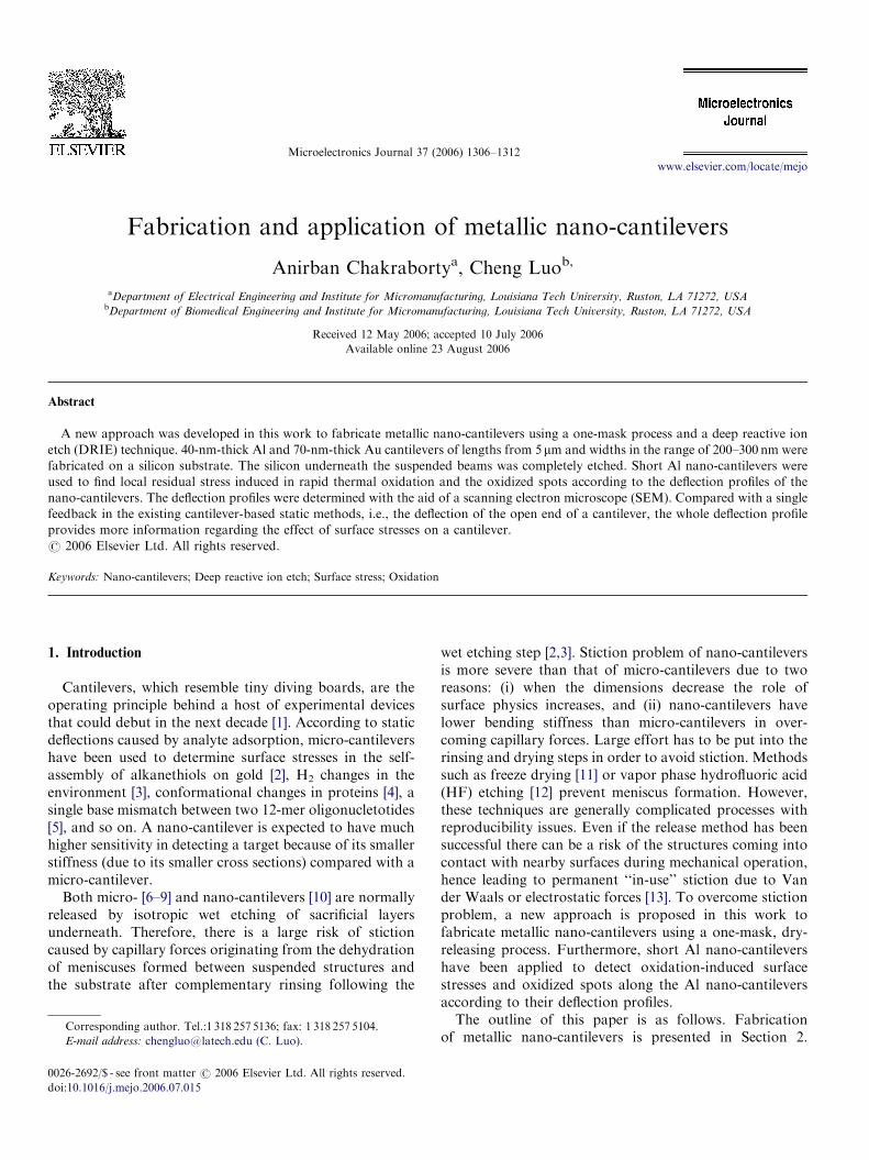
The proposed method of fabricating metal-cantileversincludes three fabrication steps: (1) spin-coat a 100-nm-thick polymethyl methacrylate (PMMA) of a molecularweight of 495K on a silicon wafer, and pattern it in theanchor-beam shape using electron-beam lithography(Fig. 1a), (2) deposit a thin metallic layer on the PMMAby thermal evaporation or sputtering, and transfer thePMMA pattern to the metallic layer by an ultrasonic-agitation assisted lift-off process (Fig. 1b), and (3) obtainmetallic nano-cantilevers using DRIE (Fig. 1c).
The key fabrication technique used in the method isDRIE, while other techniques are conventional ones inelectron-beam lithography [14–16]. In the third fabricationstep, silicon underneath metallic nano-cantilevers wasetched based on the cyclical nature of DRIE [17]. DRIEis a dry-etching technique commonly used in the area ofmicro-electro-mechanical systems to etch deep, high-aspect-ratio trenches in silicon by alternating an SF6
plasma etch with a C4F8 deposition. The etch cuts circularsections out of the silicon sidewalls while the depositionprotects already-etched sections from further destruction.As a consequence of these repeated and alternating effects,trench sidewalls are not smooth and periodically featureso-called scallops. This is an undesired property of DRIE
PMMA
Si
Nano-beam
Micro-anchor
Metal
Metallic nano-cantilever
Si
(a)
(b)
(c)
Fig. 1. Three-step procedure to fabricate an array of metallic nano-
cantilevers: (a) spin-coat a PMMA thin film on a silicon wafer, and pattern
the thin film in the anchor-beam shape using electron-beam lithography
(top view), (b) deposit a thin metallic layer on the PMMA by thermal
evaporation or sputtering, and transfer the PMMA patterns into the
metallic layer through a lift-off process (top view), and (c) obtain metallic
nano-cantilevers using deep reactive ion etch (cross-section view).
when smooth sidewalls are preferred. However, the cyclicundercutting property is favorable for certain applications,for example, in fabrication of vertical arrays of sharp fieldemission tips [18] and silicon nanowires [19]. Depending onDRIE processing parameters, the undercutting etch can beless than 50 nm [20] or above 2mm [19]. Proper processingparameters were found in this work to etch through thesilicon structure underneath the metallic nano-beams.Al and Au nano-cantilevers were fabricated using the
three-step process. Both of them had lengths from 5 mmand widths ranging from 200 to 300 nm. The thickness ofAl nano-cantilevers is 40 nm, while that of Au nano-cantilevers is 70 nm. The Al-patterned structures out of thesecond fabrication step were etched for 5min by alternat-ing the SF6 etch (4 s) and C4F8 passivation (2 s) in eachcycle with total 50 cycles. The flow rates of SF6 and C4F8
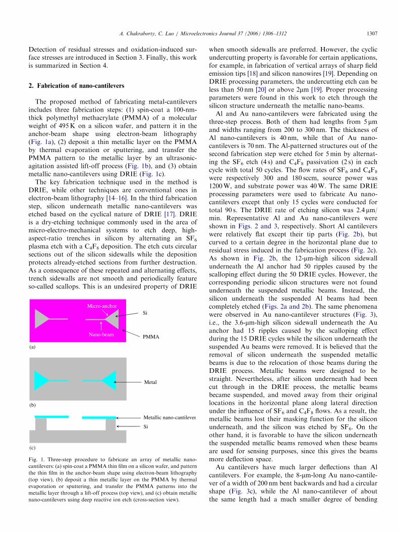
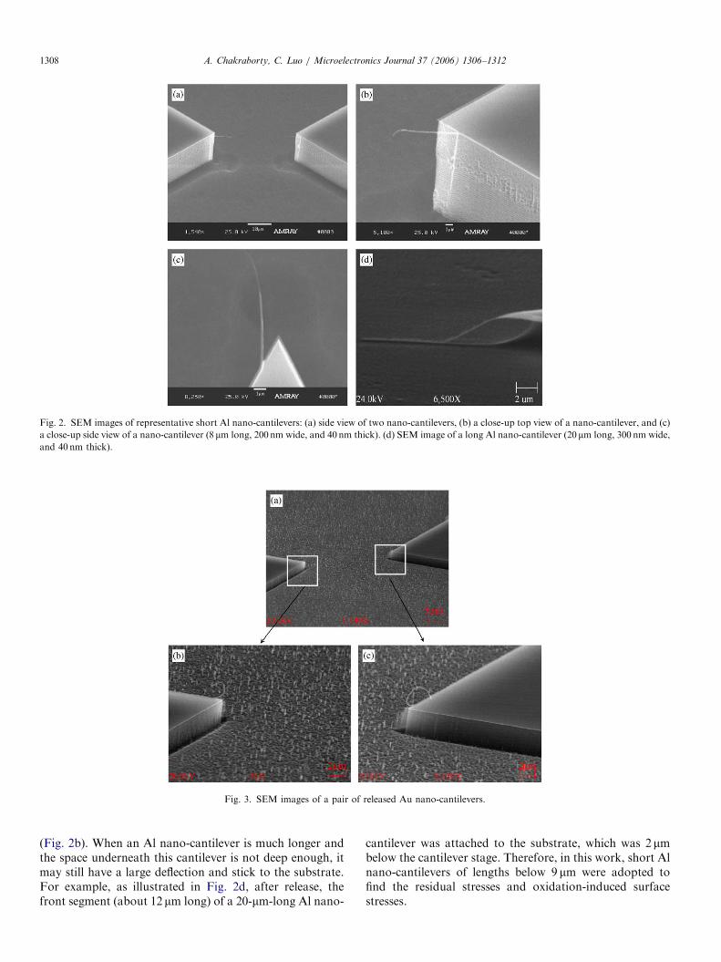
were respectively 300 and 180 sccm, source power was1200W, and substrate power was 40W. The same DRIEprocessing parameters were used to fabricate Au nano-cantilevers except that only 15 cycles were conducted fortotal 90 s. The DRIE rate of etching silicon was 2.4 mm/min. Representative Al and Au nano-cantilevers wereshown in Figs. 2 and 3, respectively. Short Al cantileverswere relatively flat except their tip parts (Fig. 2b), butcurved to a certain degree in the horizontal plane due toresidual stress induced in the fabrication process (Fig. 2c).As shown in Fig. 2b, the 12-mm-high silicon sidewallunderneath the Al anchor had 50 ripples caused by thescalloping effect during the 50 DRIE cycles. However, thecorresponding periodic silicon structures were not foundunderneath the suspended metallic beams. Instead, thesilicon underneath the suspended Al beams had beencompletely etched (Figs. 2a and 2b). The same phenomenawere observed in Au nano-cantilever structures (Fig. 3),i.e., the 3.6-mm-high silicon sidewall underneath the Auanchor had 15 ripples caused by the scalloping effectduring the 15 DRIE cycles while the silicon underneath thesuspended Au beams were removed. It is believed that theremoval of silicon underneath the suspended metallicbeams is due to the relocation of those beams during theDRIE process. Metallic beams were designed to bestraight. Nevertheless, after silicon underneath had beencut through in the DRIE process, the metallic beamsbecame suspended, and moved away from their originallocations in the horizontal plane along lateral directionunder the influence of SF6 and C4F8 flows. As a result, themetallic beams lost their masking function for the siliconunderneath, and the silicon was etched by SF6. On theother hand, it is favorable to have the silicon underneaththe suspended metallic beams removed when these beamsare used for sensing purposes, since this gives the beamsmore deflection space.Au cantilevers have much larger deflections than Al
cantilevers. For example, the 8-mm-long Au nano-cantile-ver of a width of 200 nm bent backwards and had a circularshape (Fig. 3c), while the Al nano-cantilever of aboutthe same length had a much smaller degree of bending
ARTICLE IN PRESS
Fig. 2. SEM images of representative short Al nano-cantilevers: (a) side view of two nano-cantilevers, (b) a close-up top view of a nano-cantilever, and (c)
a close-up side view of a nano-cantilever (8 mm long, 200 nm wide, and 40 nm thick). (d) SEM image of a long Al nano-cantilever (20 mm long, 300 nm wide,
and 40 nm thick).
Fig. 3. SEM images of a pair of released Au nano-cantilevers.
A. Chakraborty, C. Luo / Microelectronics Journal 37 (2006) 1306–13121308
(Fig. 2b). When an Al nano-cantilever is much longer andthe space underneath this cantilever is not deep enough, itmay still have a large deflection and stick to the substrate.For example, as illustrated in Fig. 2d, after release, thefront segment (about 12 mm long) of a 20-mm-long Al nano-
cantilever was attached to the substrate, which was 2 mmbelow the cantilever stage. Therefore, in this work, short Alnano-cantilevers of lengths below 9 mm were adopted tofind the residual stresses and oxidation-induced surfacestresses.
ARTICLE IN PRESS
CA
z
L
B x
2L
o
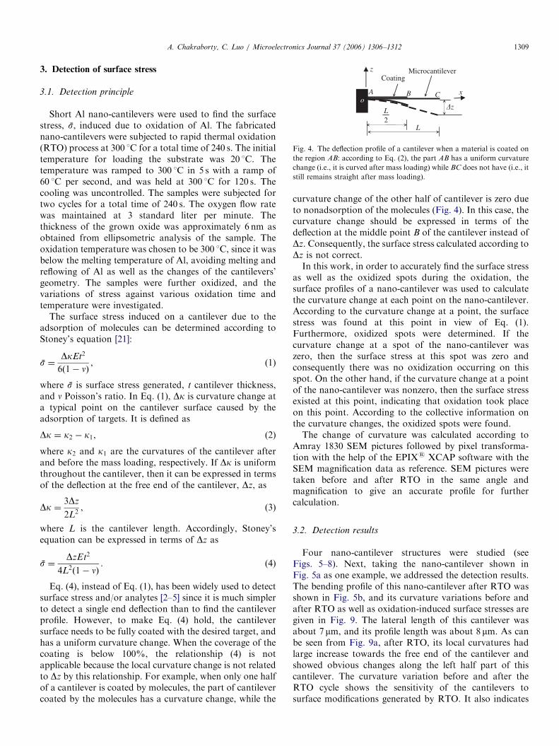
CoatingMicrocantilever
�z
Fig. 4. The deflection profile of a cantilever when a material is coated on
the region AB: according to Eq. (2), the part AB has a uniform curvature
change (i.e., it is curved after mass loading) while BC does not have (i.e., it
still remains straight after mass loading).
A. Chakraborty, C. Luo / Microelectronics Journal 37 (2006) 1306–1312 1309
3. Detection of surface stress
3.1. Detection principle
Short Al nano-cantilevers were used to find the surfacestress, s, induced due to oxidation of Al. The fabricatednano-cantilevers were subjected to rapid thermal oxidation(RTO) process at 300 1C for a total time of 240 s. The initialtemperature for loading the substrate was 20 1C. Thetemperature was ramped to 300 1C in 5 s with a ramp of60 1C per second, and was held at 300 1C for 120 s. Thecooling was uncontrolled. The samples were subjected fortwo cycles for a total time of 240 s. The oxygen flow ratewas maintained at 3 standard liter per minute. Thethickness of the grown oxide was approximately 6 nm asobtained from ellipsometric analysis of the sample. Theoxidation temperature was chosen to be 300 1C, since it wasbelow the melting temperature of Al, avoiding melting andreflowing of Al as well as the changes of the cantilevers’geometry. The samples were further oxidized, and thevariations of stress against various oxidation time andtemperature were investigated.
The surface stress induced on a cantilever due to theadsorption of molecules can be determined according toStoney’s equation [21]:
s ¼DkEt2
6ð1� nÞ, (1)
where s is surface stress generated, t cantilever thickness,and n Poisson’s ratio. In Eq. (1), Dk is curvature change ata typical point on the cantilever surface caused by theadsorption of targets. It is defined as
Dk ¼ k2 � k1, (2)
where k2 and k1 are the curvatures of the cantilever afterand before the mass loading, respectively. If Dk is uniformthroughout the cantilever, then it can be expressed in termsof the deflection at the free end of the cantilever, Dz, as
Dk ¼3Dz
2L2, (3)
where L is the cantilever length. Accordingly, Stoney’sequation can be expressed in terms of Dz as
s ¼DzEt2
4L2ð1� nÞ. (4)
Eq. (4), instead of Eq. (1), has been widely used to detectsurface stress and/or analytes [2–5] since it is much simplerto detect a single end deflection than to find the cantileverprofile. However, to make Eq. (4) hold, the cantileversurface needs to be fully coated with the desired target, andhas a uniform curvature change. When the coverage of thecoating is below 100%, the relationship (4) is notapplicable because the local curvature change is not relatedto Dz by this relationship. For example, when only one halfof a cantilever is coated by molecules, the part of cantilevercoated by the molecules has a curvature change, while the
curvature change of the other half of cantilever is zero dueto nonadsorption of the molecules (Fig. 4). In this case, thecurvature change should be expressed in terms of thedeflection at the middle point B of the cantilever instead ofDz. Consequently, the surface stress calculated according toDz is not correct.In this work, in order to accurately find the surface stress
as well as the oxidized spots during the oxidation, thesurface profiles of a nano-cantilever was used to calculatethe curvature change at each point on the nano-cantilever.According to the curvature change at a point, the surfacestress was found at this point in view of Eq. (1).Furthermore, oxidized spots were determined. If thecurvature change at a spot of the nano-cantilever waszero, then the surface stress at this spot was zero andconsequently there was no oxidization occurring on thisspot. On the other hand, if the curvature change at a pointof the nano-cantilever was nonzero, then the surface stressexisted at this point, indicating that oxidation took placeon this point. According to the collective information onthe curvature changes, the oxidized spots were found.The change of curvature was calculated according to
Amray 1830 SEM pictures followed by pixel transforma-tion with the help of the EPIXs XCAP software with theSEM magnification data as reference. SEM pictures weretaken before and after RTO in the same angle andmagnification to give an accurate profile for furthercalculation.
3.2. Detection results
Four nano-cantilever structures were studied (seeFigs. 5–8). Next, taking the nano-cantilever shown inFig. 5a as one example, we addressed the detection results.The bending profile of this nano-cantilever after RTO wasshown in Fig. 5b, and its curvature variations before andafter RTO as well as oxidation-induced surface stresses aregiven in Fig. 9. The lateral length of this cantilever wasabout 7 mm, and its profile length was about 8 mm. As canbe seen from Fig. 9a, after RTO, its local curvatures hadlarge increase towards the free end of the cantilever andshowed obvious changes along the left half part of thiscantilever. The curvature variation before and after theRTO cycle shows the sensitivity of the cantilevers tosurface modifications generated by RTO. It also indicates
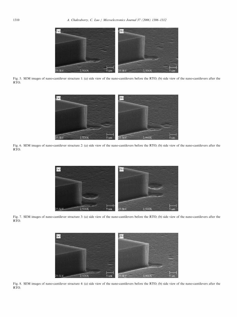
ARTICLE IN PRESS
Fig. 5. SEM images of nano-cantilever structure 1: (a) side view of the nano-cantilevers before the RTO; (b) side view of the nano-cantilevers after the
RTO.
Fig. 6. SEM images of nano-cantilever structure 2: (a) side view of the nano-cantilevers before the RTO; (b) side view of the nano-cantilevers after the
RTO.
Fig. 7. SEM images of nano-cantilever structure 3: (a) side view of the nano-cantilevers before the RTO; (b) side view of the nano-cantilevers after the
RTO.
Fig. 8. SEM images of nano-cantilever structure 4: (a) side view of the nano-cantilevers before the RTO; (b) side view of the nano-cantilevers after the
RTO.
A. Chakraborty, C. Luo / Microelectronics Journal 37 (2006) 1306–13121310
ARTICLE IN PRESS
-0.6
-0.5
-0.4
-0.3
-0.2
-0.1
0
0.1
0.2
0.3
-1
0
1
1
2
2
3
3
4
4
5
5
6
6
7
7
8
8
9
0
1 2 3 4 5 6 7 80
Length (µm)
Surf
ace
stre
ss (
N/m
)
Local curvaturebefore RTO
Length (µm)
Cur
vatu
re (
1/µm
)
Local curvatureafter RTO
(a)
(b)
x
y
x
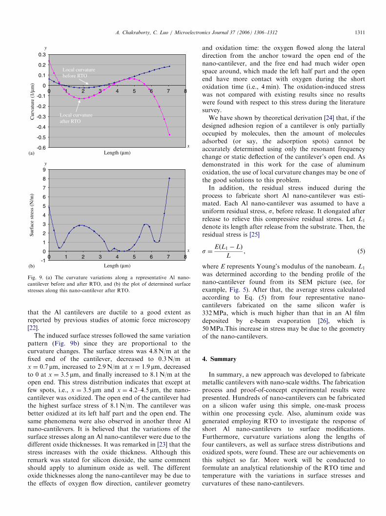
y
Fig. 9. (a) The curvature variations along a representative Al nano-
cantilever before and after RTO, and (b) the plot of determined surface
stresses along this nano-cantilever after RTO.
A. Chakraborty, C. Luo / Microelectronics Journal 37 (2006) 1306–1312 1311
that the Al cantilevers are ductile to a good extent asreported by previous studies of atomic force microscopy[22].
The induced surface stresses followed the same variationpattern (Fig. 9b) since they are proportional to thecurvature changes. The surface stress was 4.8N/m at thefixed end of the cantilever, decreased to 0.3N/m atx ¼ 0.7 mm, increased to 2.9N/m at x ¼ 1.9 mm, decreasedto 0 at x ¼ 3.5 mm, and finally increased to 8.1N/m at theopen end. This stress distribution indicates that except atfew spots, i.e., x ¼ 3.5 mm and x ¼ 4.2–4.5 mm, the nano-cantilever was oxidized. The open end of the cantilever hadthe highest surface stress of 8.1N/m. The cantilever wasbetter oxidized at its left half part and the open end. Thesame phenomena were also observed in another three Alnano-cantilevers. It is believed that the variations of thesurface stresses along an Al nano-cantilever were due to thedifferent oxide thicknesses. It was remarked in [23] that thestress increases with the oxide thickness. Although thisremark was stated for silicon dioxide, the same commentshould apply to aluminum oxide as well. The differentoxide thicknesses along the nano-cantilever may be due tothe effects of oxygen flow direction, cantilever geometry
and oxidation time: the oxygen flowed along the lateraldirection from the anchor toward the open end of thenano-cantilever, and the free end had much wider openspace around, which made the left half part and the openend have more contact with oxygen during the shortoxidation time (i.e., 4min). The oxidation-induced stresswas not compared with existing results since no resultswere found with respect to this stress during the literaturesurvey.We have shown by theoretical derivation [24] that, if the
designed adhesion region of a cantilever is only partiallyoccupied by molecules, then the amount of moleculesadsorbed (or say, the adsorption spots) cannot beaccurately determined using only the resonant frequencychange or static deflection of the cantilever’s open end. Asdemonstrated in this work for the case of aluminumoxidation, the use of local curvature changes may be one ofthe good solutions to this problem.In addition, the residual stress induced during the
process to fabricate short Al nano-cantilever was esti-mated. Each Al nano-cantilever was assumed to have auniform residual stress, s, before release. It elongated afterrelease to relieve this compressive residual stress. Let L1
denote its length after release from the substrate. Then, theresidual stress is [25]
s ¼EðL1 � LÞ
L, (5)
where E represents Young’s modulus of the nanobeam. L1
was determined according to the bending profile of thenano-cantilever found from its SEM picture (see, forexample, Fig. 5). After that, the average stress calculatedaccording to Eq. (5) from four representative nano-cantilevers fabricated on the same silicon wafer is332MPa, which is much higher than that in an Al filmdeposited by e-beam evaporation [26], which is50MPa.This increase in stress may be due to the geometryof the nano-cantilevers.
4. Summary
In summary, a new approach was developed to fabricatemetallic cantilevers with nano-scale widths. The fabricationprocess and proof-of-concept experimental results werepresented. Hundreds of nano-cantilevers can be fabricatedon a silicon wafer using this simple, one-mask processwithin one processing cycle. Also, aluminum oxide wasgenerated employing RTO to investigate the response ofshort Al nano-cantilevers to surface modifications.Furthermore, curvature variations along the lengths offour cantilevers, as well as surface stress distributions andoxidized spots, were found. These are our achievements onthis subject so far. More work will be conducted toformulate an analytical relationship of the RTO time andtemperature with the variations in surface stresses andcurvatures of these nano-cantilevers.
ARTICLE IN PRESSA. Chakraborty, C. Luo / Microelectronics Journal 37 (2006) 1306–13121312
References
[1] A. Hellemans, Cantilever tales, Science 290 (2000) 1529.
[2] R. Berger, E. Delamarche, H.P. Lang, C. Gerber, J.K. Gimzewski, E.
Meyer, J.-J. Guntherdot, Surface stress in the self-assembly of
alkanethiols on gold, Science 276 (1997) 2021–2024.
[3] H.P. Lang, R. Berger, F. Battiston, J.-P. Ramseyer, E. Meyer, C.
Andreoli, J. Brugger, P. Vettiger, M. Despont, T. Mezzacasa, L.
Scandella, H.-J. Guntherdot, Ch. Gerber, J.K. Gimzewski, A
chemical sensor based on a micromechanical cantilever array for
the identification of gases and vapors, Appl. Phys. A 66 (1998)
S61–S64.
[4] A.M. Moulin, S.J. O’Shea, R.A. Badley, P. Doyle, M.E. Welland,
Measuring surface-induced conformational changes in protein,
Langmuir 15 (1999) 8776–8779.
[5] J. Fritz, M.K. Baller, H.P. Lang, H. Rothuizen, P. Vettiger, E.
Meyer, H.J. Guntherodt, C. Gerber, J.K. Gimzewski, Translating
biomolecular recognition into nanomechanics, Science 288 (2000)
316–318.
[6] Z. Yang, X. Li, Y. Wang, H. Bao, M. Liu, Micro cantilever probe
array integrated with Piezoresistive sensor, Microelectron. J. 35
(2004) 479–483.
[7] W. Dong, X. Zhang, C. Liu, M. Li, B. Xu, W. Chen, Mechanism for
convex corner undercutting of (110) silicon in KOH, Microelectron.
J. 35 (2004) 417–419.
[8] D. Saya, K. Fukushima, H. Toshiyoshi, G. Hashiguchi, H. Fujita, H.
Kawakatsu, Fabrication of single-crystal Si cantilever array, Sensors
Actuators A 95 (2002) 281–287.
[9] R.P. Keatch, B. Lawrenson, A microstructure for detecting the stress
distribution in thin coatings deposited on to silicon substrates,
Microelectron. J. 25 (1994) 393–400.
[10] Z.J. Davis, G. Abadal, O. Kuhn, O. Hansen, F. Grey, A. Boisen,
Fabrication and characterization of nanoresonating devices for mass
detection, J. Vac. Sci. Technol. B 18 (2000) 2612–2616.
[11] E. Forsen, Z.J. Davis, M. Dong, S.G. Nilsson, L. Montelius, A.
Boisen, Dry release of suspended nanostructures, Microelectron. Eng.
73-74 (2004) 487–490.
[12] Y.I. Lee, K.H. Park, J. Lee, C.S. Lee, H.J. Yoo, C.J. Kim, Y.S.
Yoon, Dry Release for Surface Micromachining with HF Vapor-
Phase Etching, J. Microelectromech. Syst. 6 (1997) 3226–3233.
[13] N. Tas N, T. Sonnenberg, H. Jansen, R. Legtenberg, M. Elwenspoek,
Stiction in surface micromachining, J. Micromech. Microeng. 6
(1996) 385–397.
[14] Y. Shacham-Diamand, 100 nm wide copper lines made by selective
electroless deposition, J. Micromech. Microeng. 1 (1991) 66–72.
[15] S. Yasin, D.G. Hasko, H. Ahmed, Fabrication of A5 nm width lines
in polyNmethylmethacrylateO resist using a water:isopropyl alcohol
developer and ultrasonically-assisted development, Appl. Phys. Lett.
78 (2001) 2760–2762.
[16] D.H. Kim, D.S. Cho, K. Jang, C.D. Kim, H.R. Lee, The growth of
freestanding single carbon nanotube arrays, Nanotechnology 14
(2003) 1269–1271.
[17] R. Bosch Gmbh,patents 4855017 and 4784720 (USA).
[18] V. Milanovic, L. Doherty, D. Teasdale, S. Parsa, C. Zhang, K. Pister,
Micromachining technology for lateral field emission devices, IEEE
Trans. Electron Dev. 48 (2001) 166–172.
[19] L. Doherty, V. Milanovic, A simple process for lateral single crystal
silicon nanowires, Proceedings of IMECE’02 New Orleans Louisiana,
2002, pp. 17–22.
[20] N. Maluf, An Introduction to Microlectrical Systems Engineering,
Artech House, Boston, 2000.
[21] G.G. Stoney, The tension of metallic films deposited by electrolysis,
Proc. R. Soc. London A 82 (1909) 172–177.
[22] S.G. Nilsson, E.L. Sarwe, L. Montelius, Fabrication and mechanical
characterization of ultrashort nanocantilevers, Appl. Phys. Lett. 83
(2003) 990–992.
[23] D.-B. Kao, J.P. McVitte, W.D. Nix, K.C. Saraswat, IEEE Trans.
Electron Dev. ED 35 (1988) 25.
[24] C. Luo, Inaccuracy in the detection of molecules using two micro-
cantilever-based methods, ASME J. Appl. Mech. 72 (2005) 617–619.
[25] S.D. Senturia, Microsystem Design, Kluwer Academic Publishing,
2001, p. 215.
[26] U. Smith, N. Kristensen, F. Ericson, J.-A. Schweitz, Local stress
relaxation in thin aluminum films, J. Vac. Sci.Technol. A 9 (1991) 2527.